JP4359561B2 - Circuit and method for writing to toggle memory - Google Patents
Circuit and method for writing to toggle memory Download PDFInfo
- Publication number
- JP4359561B2 JP4359561B2 JP2004517527A JP2004517527A JP4359561B2 JP 4359561 B2 JP4359561 B2 JP 4359561B2 JP 2004517527 A JP2004517527 A JP 2004517527A JP 2004517527 A JP2004517527 A JP 2004517527A JP 4359561 B2 JP4359561 B2 JP 4359561B2
- Authority
- JP
- Japan
- Prior art keywords
- write
- toggle
- memory
- writing
- bit
- Prior art date
- Legal status (The legal status is an assumption and is not a legal conclusion. Google has not performed a legal analysis and makes no representation as to the accuracy of the status listed.)
- Expired - Fee Related
Links
Images


Classifications
-
- G—PHYSICS
- G11—INFORMATION STORAGE
- G11C—STATIC STORES
- G11C11/00—Digital stores characterised by the use of particular electric or magnetic storage elements; Storage elements therefor
- G11C11/02—Digital stores characterised by the use of particular electric or magnetic storage elements; Storage elements therefor using magnetic elements
- G11C11/14—Digital stores characterised by the use of particular electric or magnetic storage elements; Storage elements therefor using magnetic elements using thin-film elements
- G11C11/15—Digital stores characterised by the use of particular electric or magnetic storage elements; Storage elements therefor using magnetic elements using thin-film elements using multiple magnetic layers
-
- G—PHYSICS
- G11—INFORMATION STORAGE
- G11C—STATIC STORES
- G11C11/00—Digital stores characterised by the use of particular electric or magnetic storage elements; Storage elements therefor
- G11C11/02—Digital stores characterised by the use of particular electric or magnetic storage elements; Storage elements therefor using magnetic elements
- G11C11/16—Digital stores characterised by the use of particular electric or magnetic storage elements; Storage elements therefor using magnetic elements using elements in which the storage effect is based on magnetic spin effect
- G11C11/165—Auxiliary circuits
- G11C11/1675—Writing or programming circuits or methods
-
- G—PHYSICS
- G11—INFORMATION STORAGE
- G11C—STATIC STORES
- G11C11/00—Digital stores characterised by the use of particular electric or magnetic storage elements; Storage elements therefor
-
- G—PHYSICS
- G11—INFORMATION STORAGE
- G11C—STATIC STORES
- G11C11/00—Digital stores characterised by the use of particular electric or magnetic storage elements; Storage elements therefor
- G11C11/02—Digital stores characterised by the use of particular electric or magnetic storage elements; Storage elements therefor using magnetic elements
- G11C11/16—Digital stores characterised by the use of particular electric or magnetic storage elements; Storage elements therefor using magnetic elements using elements in which the storage effect is based on magnetic spin effect
- G11C11/165—Auxiliary circuits
- G11C11/1653—Address circuits or decoders
- G11C11/1655—Bit-line or column circuits
-
- G—PHYSICS
- G11—INFORMATION STORAGE
- G11C—STATIC STORES
- G11C11/00—Digital stores characterised by the use of particular electric or magnetic storage elements; Storage elements therefor
- G11C11/02—Digital stores characterised by the use of particular electric or magnetic storage elements; Storage elements therefor using magnetic elements
- G11C11/16—Digital stores characterised by the use of particular electric or magnetic storage elements; Storage elements therefor using magnetic elements using elements in which the storage effect is based on magnetic spin effect
- G11C11/165—Auxiliary circuits
- G11C11/1653—Address circuits or decoders
- G11C11/1657—Word-line or row circuits
-
- G—PHYSICS
- G11—INFORMATION STORAGE
- G11C—STATIC STORES
- G11C2207/00—Indexing scheme relating to arrangements for writing information into, or reading information out from, a digital store
- G11C2207/22—Control and timing of internal memory operations
- G11C2207/2263—Write conditionally, e.g. only if new data and old data differ
Abstract
Description
本発明はメモリへの書き込みに関し、より詳細にはトグルするメモリへの書き込みに関する。 The present invention relates to writing to memory, and more particularly to writing to toggled memory.
不揮発性メモリ装置は、電子システムの非常に重要な構成部品である。FLASHは現在使用されている主要な不揮発性メモリ装置である。通常の不揮発性メモリ装置は、浮遊酸素層に捕獲された電荷を用いて情報を格納する。FLASHメモリの欠点としては、高電圧要件および遅いプログラム時間および消去時間がある。また、FLASHメモリは書き換え耐久性が低く、104〜106サイクルでメモリが故障してしまう。また、妥当なデータ保持を維持するために、ゲート酸化膜のスケーリングは電子が受ける(see )トンネル障壁によって制限される。よって、FLASHメモリの寸法は、スケーリングすることのできる範囲に制限される。 Non-volatile memory devices are very important components of electronic systems. FLASH is the main non-volatile memory device currently in use. A normal nonvolatile memory device stores information using charges trapped in the floating oxygen layer. Disadvantages of FLASH memory include high voltage requirements and slow program and erase times. Further, FLASH memory has low rewriting durability, and the memory fails in 10 4 to 10 6 cycles. Also, in order to maintain reasonable data retention, gate oxide scaling is limited by the tunnel barriers that the electrons see. Therefore, the size of the FLASH memory is limited to a range that can be scaled.
これらの欠点を克服するために、磁気メモリ装置が評価されている。このような装置の1つに、磁気抵抗RAM(以下では「MRAM」と呼ぶ)がある。しかし、商業的に実用的なものとするには、MRAMは、現在のメモリ技術に匹敵するメモリ密度を有し、将来の生産に関してスケーラブルであり、低電圧で動作し、電力消費量が低く、匹敵する読み取り/書き込み速度を有しなければならない。 In order to overcome these drawbacks, magnetic memory devices are being evaluated. One such device is a magnetoresistive RAM (hereinafter referred to as “MRAM”). However, to be commercially practical, MRAM has a memory density comparable to current memory technology, is scalable for future production, operates at low voltage, has low power consumption, Must have comparable read / write speeds.
MRAM装置の場合、その設計特性の最も重要な側面として、不揮発性メモリの状態の安定性、読み取り/書き込みサイクルの繰り返し性、およびメモリエレメント間のスイッチング磁界の均一性の3つがある。MRAMのメモリ状態は、電力によって維持されるのではなく、磁気モーメントベクトルの方向によって維持される。データの格納は、磁界を印加し、MRAM装置の磁性体を2つの可能なメモリ状態のいずれかに磁化させることによって達成される。データの呼び出しは、MRAM装置における2つの状態間の抵抗差を検知することによって達成される。書き込みのための磁界は、磁気構造外部のストリップ線または磁気構造自体に電流を流すことによって生成される。 In the case of an MRAM device, the three most important aspects of its design characteristics are the non-volatile memory state stability, read / write cycle repeatability, and uniformity of the switching field between memory elements. The memory state of the MRAM is not maintained by power but by the direction of the magnetic moment vector. Data storage is accomplished by applying a magnetic field and magnetizing the magnetic body of the MRAM device to one of two possible memory states. Data recall is accomplished by sensing the resistance difference between two states in the MRAM device. The magnetic field for writing is generated by passing a current through a strip line outside the magnetic structure or the magnetic structure itself.
MRAM装置の横寸法が小さくなるにつれて、3つの問題が生じる。第1に、所与の形状および膜厚に対するスイッチング磁界が大きくなり、スイッチングにより大きな磁界を必要とする。第2に、全体のスイッチング量が減り、反転のためのエネルギー障壁が減る。エネルギー障壁とは、磁気モーメントベクトルを或る状態からもう一方の状態にスイッチングさせるために必要なエネルギーの量を指す。エネルギー障壁により、MRAM装置のデータ保持および誤り率が決まり、障壁が小さすぎる場合、熱変動(超常磁性)により意図しない反転が生じる可能性がある。エネルギー障壁が小さいことに伴う主な問題は、アレイ内の1つのMRAM装置を選択的にスイッチングさせることが非常に難しくなることである。選択性により、他のMRAM装置を意図せずスイッチングすることなくスイッチングを行うことができる。最後に、スイッチング磁界は、形状により生成されるため、MRAM装置のサイズが小さくなるにつれて形状の変化により敏感になる。フォトリソグラフィーによるスケーリングは小さな寸法になるほど難しくなるため、MRAM装置は、密なスイッチング分布を維持することが難しくなるであろう。 As the lateral dimensions of the MRAM device become smaller, three problems arise. First, the switching magnetic field for a given shape and film thickness is large and requires a large magnetic field for switching. Second, the total amount of switching is reduced and the energy barrier for inversion is reduced. An energy barrier refers to the amount of energy required to switch a magnetic moment vector from one state to another. The energy barrier determines the data retention and error rate of the MRAM device, and if the barrier is too small, unintentional inversion may occur due to thermal fluctuations (superparamagnetism). The main problem with the small energy barrier is that it becomes very difficult to selectively switch one MRAM device in the array. With selectivity, switching can be performed without unintentionally switching other MRAM devices. Finally, since the switching field is generated by shape, it becomes more sensitive to shape changes as the size of the MRAM device decreases. MRAM devices will have difficulty maintaining a dense switching distribution because photolithography scaling becomes more difficult with smaller dimensions.
したがって、従来技術にあった上記および他の欠点を改善することが非常に有利であろう。 Therefore, it would be highly advantageous to remedy the above and other drawbacks of the prior art.
本発明の上記およびさらなるより具体的な目的および利点は、当業者には、添付図面とともに解釈される以下の本発明の好適な実施形態の詳細な説明から容易に明らかとなるであろう。 The above and further more specific objects and advantages of the present invention will be readily apparent to those skilled in the art from the following detailed description of the preferred embodiments of the present invention, taken in conjunction with the accompanying drawings.
トグルメモリは、メモリセルの状態を反転させるか、あるいはメモリセルを同一の論理状態のままにしておくことによって書き込まれる。これらのどちらが選択されたかを判定するためには、書き込むべき論理状態を既存の状態と比較しなければならない。この場合、書き込みシーケンスは、この比較が完了する前に開始される。比較の結果が、論理状態を反転すべきであるというものである場合、書き込みシーケンスを続行する。論理状態を同一のままとすべき場合、書き込みシーケンスを終了する。 Toggle memory is written by inverting the state of the memory cell or by leaving the memory cell in the same logic state. In order to determine which of these has been selected, the logic state to be written must be compared with the existing state. In this case, the write sequence is started before this comparison is completed. If the result of the comparison is that the logic state should be reversed, the write sequence is continued. If the logic state should remain the same, the write sequence ends.
次に図1を参照して、図1は、本発明の好適な実施形態によるMRAMアレイ3の略断面図を示す。この例では、単一の磁気抵抗メモリ装置10のみを示すが、MRAMアレイ3はいくつかのMRAM装置10からなり、本発明では、書き込み方法の説明を簡潔にするために、そのような装置を1つだけ示していることが理解されるであろう。
Reference is now made to FIG. 1, which shows a schematic cross-sectional view of an
MRAM装置10は、書き込みワード線20および書き込みビット線30を備える。書き込みワード線20および書き込みビット線30は、電流を流すことができるように導電体を含む。この例示において、書き込みワード線20はMRAM装置10の上部に配置され、書き込みビット線30はMRAM装置10の下部に配置されて、ワード線20に対して90°の角度に向けられる(図2を参照)。代替として、書き込みワード線20はMRAM装置10の下部に配置されてもよく、書き込みビット線30はMRAM装置10の上部に配置されてもよい。
The
MRAM装置10は、第1の磁性体領域15、トンネル障壁16、および第2の磁性体領域17を含むトンネル接合部を備え、トンネル障壁16は第1の磁性体領域15と第2の磁性体領域17の間に挟まれる。好適な実施形態において、磁性体領域15は、2つの強磁性体層45および55の間の反強磁性体結合スペーサ層65を有する三層構造18を含む。反強磁性体結合スペーサ層65は厚さ86を有し、強磁性体層45および55はそれぞれ厚さ41および51を有する。さらに、磁性体領域17は、2つの強磁性体層46および56の間の反強磁性体結合スペーサ層66を有する三層構造19を有する。反強磁性体結合スペーサ層66は厚さ87を有し、強磁性体層46および56はそれぞれ厚さ42および52を有する。
The
一般に、反強磁性体結合スペーサ層65および66は、Ru、Os、Re、Cr、Rh、Cu、またはそれらの組み合わせの元素のうちの少なくとも1つを含む。さらに、強磁性体層45、55、46、および56は、Ni、Fe、Mn、Co、またはそれらの組み合わせの元素のうちの少なくとも1つを含む。また、磁性体領域15および17は、三層構造以外の合成反強磁性体(SAF)層構造を含むこともでき、本実施形態での三層構造の使用は例示目的に過ぎないことが理解されるであろう。例えば、そのような合成反強磁性体層構造の1つとして、強磁性体層/反強磁性体結合スペーサ層/強磁性体層/反強磁性体結合スペーサ層/強磁性体層の構造である五層の積層体が含まれる可能性がある。
In general, antiferromagnetically coupled
強磁性体層45および55はそれぞれ、反強磁性体結合スペーサ層65の結合により通常は反平行に保持される磁気モーメントベクトル57および53を有する。また、磁性体領域15は、結果として生じる磁気モーメントベクトル40を有し、磁性体領域17は、結果として生じる磁気モーメントベクトル50を有する。結果として生じる磁気モーメントベクトル40および50は、書き込みワード線20および書き込みビット線30から或る角度、好ましくは45°の方向にある異方性の容易軸に沿って配向している(図2を参照)。さらに、磁性体領域15は浮遊強磁性体領域である、すなわち、結果として生じる
磁気モーメントベクトル40が、磁界が印加されていても自由に回転できる。磁性体領域17はピン止め(pin :固定)された強磁性体領域である、すなわち、結果として生じる磁気モーメントベクトル50が、適度な磁界が印加された状態では自由に回転できず、基準層として用いられる。
各三層構造18において2つの強磁性体層の間にある反強磁性体結合層を示すが、強磁性体層は、静磁界または他の特徴といった他の手段により反強磁性体結合されることもできることが理解されるであろう。例えば、セルのアスペクト比を5以下に小さくした場合、強磁性体層は、静磁束還流(magnetostatic flux closure)により反平行結合される。
Each
好適な実施形態において、MRAM装置10は、非円形の平面の場合に長さ/幅の比が1〜5の範囲である三層構造18を有する。しかし、本発明では円形の平面を示す(図2を参照)。MRAM装置10は好適な実施形態において、形状異方性によるスイッチング磁界への貢献を最小化するために、また、フォトリソグラフィー加工を用いて装置をより小さな横寸法にスケーリングするほうが容易であるために円形形状である。しかし、MRAM装置10は他の形状、例えば正方形、楕円形、長方形、またはひし形とすることができるものの、簡略化のために円形のものとして図示されることが理解されるであろう。
In a preferred embodiment, the
さらに、MRAMアレイ3の作製中、それ以後の各層(すなわち30、55、65等)は、順に堆積または他の方法で形成され、各MRAM装置10は、半導体業界において既知の技法のいずれかで選択的堆積、フォトリソグラフィー加工、エッチング等によって画定されてもよい。少なくとも強磁性体層45および55の堆積中に、このペアに優先(preferred )磁気容易軸を設定するために磁界が与えられる(誘導異方性)。与えられた磁界は、磁気モーメントベクトル53および57に優先異方性軸を生じる。優先軸は、じきに説明するように、書き込みワード線20と書き込みビット線30の間で45°の角度となるように選択される。
In addition, during fabrication of the
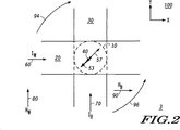
次に図2を参照して、図2は、本発明によるMRAMアレイ3の略平面図を示す。MRAM装置10の説明を簡略化するために、全ての方向は、図示のようなxおよびy座標系100ならびに時計回り方向94および反時計回り方向96を基準にする。説明をさらに簡略化するために、ここで再度、Nは2に等しく、MRAM装置10が、磁気モーメントベクトル53および57ならびに結果として生じる磁気モーメントベクトル40を有する領域15において1つの三層構造を含むものと仮定する。また、磁気モーメントベクトルはスイッチングされるため、領域15の磁気モーメントベクトルのみを図示する。
Reference is now made to FIG. 2, which shows a schematic plan view of an
書き込み方法がどのように機能するかを例示するために、磁気モーメントベクトル53および57の優先異方性軸は、負のx方向および負のy方向に対して45°の角度、および正のx方向および正のy方向に対して45°の角度の向きにあると仮定する。一例として、図2は、磁気モーメントベクトル53が負のx方向および負のy方向に対して45°の角度の向きにあることを示す。磁気モーメントベクトル57は通常、磁気モーメントベクトル53に対して反平行に配向されるため、正のx方向および正のy方向に対して45°の角度に方向付けされる。この初期配向は、じきに説明するように、書き込み方法の例を示すために用いられる。
To illustrate how the writing method works, the preferential anisotropy axis of the
好適な実施形態において、書き込みワード電流60は、正のx方向に流れる場合に正であるものとして定義され、書き込みビット電流70は、正のy方向に流れる場合に正であるものとして定義される。書き込みワード線20および書き込みビット線30の目的は、MRAM装置10内に磁界を生成することである。正の書き込みワード電流60は周囲の書き込みワード磁界HW80を誘導し、正の書き込みビット電流70は周囲の書き込みビット磁界HB90を誘導する。この例では、書き込みワード線20がMRAM装置10の
上にあるため、要素平面において、HW80は正の書き込みワード電流60の場合にMRAM装置10に正のy方向で印加される。同様に、書き込みビット線30はMRAM装置10の下にあるため、要素平面において、HB90は正の書き込みビット電流70の場合にMRAM装置10に正のx方向で印加される。正および負の電流の定義は任意であり、ここでは例示目的で定義されることが理解されるであろう。電流を反転させる効果は、MRAM装置10内で誘導される磁界の方向を変化させるものである。電流によって誘導される磁界の挙動は当業者にはよく知られているため、ここでさらに詳述することはしない。
In the preferred embodiment, the write word current 60 is defined as positive when flowing in the positive x direction, and the write bit current 70 is defined as positive when flowing in the positive y direction. . The purpose of the
次に図3を参照して、図3は、SAF三層構造のシミュレートされたスイッチング挙動を示す。シミュレーションは、内因性の異方性とほぼ同一のモーメント(ほぼ釣り合いの取れたSAF)を有し、反強磁性体結合され、磁化ダイナミクスがランダウ−リフシッツ(Landau-Lifshitz )方程式によって記述される2つの単磁区層からなる。x軸は、書き込みワード線の磁界の大きさ(エルステッド(1エルステッド≒79.577アンペア毎メートル))であり、y軸は、書き込みビット線の磁界の大きさ(エルステッド)である。磁界は、図4に示すようなパルスシーケンス100で印加され、パルスシーケンス100は、時間に応じた書き込みワード電流60および書き込みビット電流70を含む。
Reference is now made to FIG. 3, which shows the simulated switching behavior of the SAF tri-layer structure. The simulation has almost the same moment as intrinsic anisotropy (almost balanced SAF), is antiferromagnetically coupled, and the magnetization dynamics are described by the Landau-
図3には3つの動作領域が示されている。領域92ではスイッチングが起こらない。領域95におけるMRAM動作には、直接書き込み方法が実施される。直接書き込み方法を用いる場合、状態がスイッチングするのは、書き込まれる状態が格納されている状態と異なる場合のみであるため、MRAM装置の初期状態を判定する必要はない。書き込み状態の選択は、書き込みワード線20および書き込みビット線30の両方における電流の方向によって判定される。例えば、「1」を書き込みたい場合、両方の線の電流の方向は正になる。「1」が既に要素に格納されており、「1」が書き込まれる場合、MRAM装置の最終的な状態は「1」であり続ける。さらに、「0」が格納されており、正の電流を用いて「1」が書き込まれる場合、MRAM装置の最終的な状態は「1」となる。書き込みワード線と書き込みビット線の両方に負の電流を用いることによって、「0」を書き込む場合も同様の結果が得られる。したがって、いずれの状態であっても、初期の状態に関係なく適切な極性の電流パルスを用いて所望の「1」または「0」にプログラムすることができる。本開示を通して、領域95における動作は「直接書き込みモード」として定義される。
FIG. 3 shows three operating areas. In
領域97におけるMRAMの動作には、トグル書き込み方法が実施される。トグル書き込み方法を用いる場合、書き込みの前にMRAM装置の初期状態を判定する必要がある。これは、書き込みワード線20と書き込みビット線30の両方に同一極性の電流パルスが選択される限り、電流の方向に関係なくMRAM装置に書き込みが行われる度に状態がスイッチングするためである。例えば、「1」が最初に格納されている場合、書き込みワード線と書き込みビット線に正の電流パルスシーケンスを1回流すと、装置の状態は「0」にスイッチングされる。格納された「0」の状態に繰り返し正の電流パルスシーケンスを与えると、状態は「1」に戻る。したがって、メモリエレメントを所望の状態に書き換え(write )可能とするには、MRAM装置10の初期状態をまず読み取って、書き込むべき状態と比較しなければならない。この読み取りおよび比較は、情報を格納するバッファと、メモリ状態を比較する比較器とを含むさらなる論理回路部を必要とする場合がある。次に、格納されている状態と書き込むべき状態とが異なる場合にのみ、MRAM装置10に書き込みを行う。この方法の利点の1つに、異なるビットのみをスイッチングさせるため、消費電力が少なくなることがある。トグル書き込み方法を用いるさらなる利点として、単極電圧のみが必要であり、結果として、より小さなNチャネルトランジスタを使用してMRAM装置を駆動できることがある。本開示を通して、領域97における動作は「トグル書き込みモード」として定義される。
For the operation of the MRAM in the
両方の書き込み方法が、磁気モーメントベクトル53および57を上述のような2つの優先方向の一方に配向させることができるように、書き込みワード線20と書き込みビット線30に電流を供給することを伴う。2つのスイッチングモードを完全に説明するために、磁気モーメントベクトル53、57、および40の時間発展を説明する具体的な例を次に示す。
Both write methods involve supplying current to the
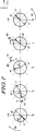
次に図5を参照すると、図5は、パルスシーケンス100を用いて「1」を「0」に書き換えるトグル書き込みモードを示す。この図の時間t0において、磁気モーメントベクトル53および57は、図2に示すような優先方向に配向している。この配向を「1」として定義する。
Next, referring to FIG. 5, FIG. 5 shows a toggle write mode in which “1” is rewritten to “0” using the
時間t1において、正の書き込みワード電流60がオンにされ、これにより、正のy方向に方向付けされるHW80を誘導する。正のHW80の作用は、ほぼ釣り合いの取れた反整列の(anti-aligned)MRAM三層構造を「フロップ」させ、印加された磁界の方向に対して約90°の配向にすることである。強磁性体層45および55間の有限の反強磁性体交換相互作用により、磁気モーメントベクトル53および57を今度は小さな角度で磁界の方向に偏向させることができ、結果として生じる磁気モーメントベクトル40は、磁気モーメントベクトル53および57の間の角度に延び(subtend )、HW80と整列する。よって、磁気モーメントベクトル53は時計回り方向94に回転する。結果として生じる磁気モーメントベクトル40は、磁気モーメントベクトル53および57のベクトル加算であるため、磁気モーメントベクトル57もまた時計回り方向94に回転する。
At time t 1 , positive write word current 60 is turned on, thereby inducing
時間t2において、正の書き込みビット電流70がオンにされ、これにより正のHB90を誘導する。その結果、結果として生じる磁気モーメントベクトル40は同時に、HW80によって正のy方向に、HB90によって正のx方向に方向付けされ、これは、有効な磁気モーメントベクトル40を時計回り方向94に、正のx方向と正のy方向の間の45°の角度に概ね配向されるまでさらに回転させる効果を持つ。その結果、磁気モーメントベクトル53および57もまた時計回り方向94にさらに回転する。
At time t 2 , positive write bit current 70 is turned on, thereby inducing
時間t3において、書き込みワード電流60がオフにされ、この場合、HB90のみが結果として生じる磁気モーメントベクトル40を方向付けし、磁気モーメントベクトル40は今、正のx方向に配向している。磁気モーメントベクトル53および57は今両方とも、異方性困難軸の不安定点を越えた角度に概ね方向付けされる。
At time t 3 , the write word current 60 is turned off, in which case only
時間t4において、書き込みビット電流70がオフにされ、磁界の力が、結果として生じる磁気モーメントベクトル40に作用しなくなる。その結果、磁気モーメントベクトル53および57は、異方性エネルギーを最小化するために、それぞれの最も近い優先方向に配向される。この場合、磁気モーメントベクトル53の優先方向は正のy方向および正のx方向に対して45°の角度にある。この優先方向はまた、時間t0における磁気モーメントベクトル53の最初の方向から180°のところにあり、「0」として定義される。よって、MRAM装置10は「0」にスイッチングされている。MRAM装置10は、書き込みワード線20と書き込みビット線30の両方に負の電流を用いることによって磁気モーメントベクトル53、57、および40を反時計回り方向96に回転させることによってもスイッチングすることができるものの、例示目的でそうでない方法で示されることが理解されるであろう。
At time t 4 , the write bit current 70 is turned off and the magnetic field force no longer acts on the resulting
次に図6を参照すると、図6は、パルスシーケンス100を用いて「0」を「1」に書き換えるトグル書き込みモードを示す。磁気モーメントベクトル53および57、ならびに結果として生じる磁気モーメントベクトル40を時間t0、t1、t2、t3、および
t4のそれぞれにおいて上述のように図示し、同一の電流および磁界方向を用いてMRAM装置10の状態を「0」から「1」にスイッチングさせる能力を示している。したがって、MRAM装置10の状態は、図3の領域97に対応するトグル書き込みモードで書き込まれる。
Next, referring to FIG. 6, FIG. 6 shows a toggle write mode in which “0” is rewritten to “1” using the
直接書き込みモードの場合、磁気モーメントベクトル53の大きさは磁気モーメントベクトル57よりも大きく、磁気モーメントベクトル40は、磁気モーメントベクトル53と同じ方向を指すが、ゼロ磁界の大きさがより小さいと仮定される。この不釣り合いなモーメントにより、印加された磁界に全モーメントを整列させる傾向がある二極エネルギーが、ほぼ釣り合いの取れたSAFの対称性を壊すことが可能になる。したがってスイッチングは、所与の極性の電流に対して1方向にしか起こり得ない。
In the direct write mode, the magnitude of the
次に図7を参照すると、図7は、直接書き込みモードを用い、パルスシーケンス100を用いて「1」を「0」に書き換える一例を示す。ここでもまた、メモリ状態は最初は「1」であり、磁気モーメントベクトル53は負のx方向および負のy方向に対して45°に方向付けされ、磁気モーメントベクトル57は正のx方向および正のy方向に対して45°に方向付けされる。上述の正の書き込みワード電流60および正の書き込みビット電流70によるパルスシーケンスに続いて、上述のトグル書き込みモードと同様の方法で書き込みが行われる。モーメントは時間t1において再び「フロップ」するが、結果として得られる角度は、不釣り合いなモーメントおよび異方性により90°から傾いていることに留意されたい。時間t4の後、MRAM装置10は「0」状態にスイッチングされており、結果として生じる磁気モーメント40は、所望通りに正のx方向および正のy方向において45°の角度に配向される。同様の結果が、「0」を「1」に書き換える場合にも得られ、ここでは負の書き込みワード電流60および負の書き込みビット電流70のみが用いられる。
Referring now to FIG. 7, FIG. 7 shows an example of rewriting “1” to “0” using the
次に図8を参照すると、図8は、直接書き込みモードを用いた書き込みの、新たな状態が既に格納されている状態と同じである場合の一例を示す。この例では、MRAM装置10に「0」が既に格納されており、ここで、電流パルスシーケンス100を繰り返して「0」を格納する。磁気モーメントベクトル53および57は、時間t1において「フロップ」しようとするが、印加された磁界に対して不釣り合いの磁気モーメントが作用しなければならないため、回転は損なわれる。よって、反転状態から回転するにはさらなるエネルギー障壁がある。時間t2において、ドミナント(dominant)モーメント53は、正のx軸とほぼ整列しており、その最初の異方性方向から45°未満である。時間t3において、磁界は正のx軸に沿って方向付けされる。さらに時計方向に回転する代わりに、システムはこの場合、印加された磁界に対するSAFモーメントの対称性を変化させることによってエネルギーを下げる。パッシブ(passive )モーメント57がx軸を越え、システムは、ドミナントモーメント53がその元の方向の近くに戻った状態で安定する。したがって、時間t4において、磁界を取り除くと、MRAM装置10に格納されている状態は「0」のままとなる。このシーケンスは、図3において領域95として示される直接書き込みモードの機構を示す。よって、この規則(convention)において、「0」を書き込むには、書き込みワード線60と書き込みビット線70の両方に正の電流が必要であり、逆に「1」を書き込むには、書き込みワード線60と書き込みビット線70の両方に負の電流が必要である。
Referring now to FIG. 8, FIG. 8 shows an example where the new state of writing using the direct write mode is the same as the state already stored. In this example, “0” is already stored in the
より大きな磁界を印加する場合、最終的に、フロップおよびシザー(scissor )に関連するエネルギー低下は、トグル事象を防止する不釣り合いなモーメントの二極エネルギーによって生じるさらなるエネルギー障壁を越える。この時点で、トグル事象が生じ、領域97によってスイッチングが記述される。
When applying a larger magnetic field, ultimately the energy drop associated with the flop and scissor exceeds the additional energy barrier caused by the unbalanced moment of bipolar energy that prevents the toggle event. At this point, a toggle event occurs and switching is described by
時間t3およびt4が等しいか、限りなく等しい状態に近づけられた場合、直接書き込みモードが適用される領域95を拡張することができる、すなわち、トグルモード領域97をより高い磁界に移動させることができる。この場合、磁界の方向は、書き込みワード電流60がオンにされたときビット異方性軸に対して45°で開始し、次に書き込みビット電流70がオンにされるとビット異方性軸に平行となるように移動する。この例は、通常の磁界印加シーケンスと同様である。しかし、ここで書き込みワード電流60と書き込みビット電流70がほぼ同時にオフになり、磁界の方向がそれ以上回転しなくなる。したがって、印加される磁界は、書き込みワード電流60と書き込みビット電流70の両方がオンになった状態で、結果として生じる磁界モーメントベクトル40がその困難軸の不安定点を既に通過しているように十分に大きくなければならない。この場合、磁界の方向がここでは、以前のような90°ではなく45°しか回転されないため、トグル書き込みモード事象が生じる可能性は低い。下降時間t3およびt4がほぼ同時であることの利点は、この場合、磁界上昇時間t1およびt2の順番にさらなる制約がないことである。したがって、磁界は任意の順番でオンにするか、あるいはほぼ同時とすることもできる。
If the times t 3 and t 4 are equal or approached as close as possible, the
上述の書き込み方法は、時間t2と時間t3の間に書き込みワード電流60と書き込みビット電流70の両方がオンにされたMRAM装置のみで状態がスイッチングするため、非常に選択的である。この特徴を図9および図10に示す。図9は、書き込みワード電流60をオンにせず書き込みビット電流70をオンにしたときのパルスシーケンス100を示す。図10は、MRAM装置10の状態の対応する挙動を示す。時間t0において、磁気モーメントベクトル53および57、ならびに結果として生じる磁気モーメントベクトル40は、図2において説明したように配向される。パルスシーケンス100において、書き込みビット電流70は時間t1においてオンにされる。この間、HB90により、結果として生じる磁気モーメントベクトル40が正のx方向に方向付けられる。
The write method described above is very selective because the state switches only in MRAM devices where both the write word current 60 and the write bit current 70 are turned on between time t 2 and time t 3 . This feature is illustrated in FIGS. FIG. 9 shows a
書き込みワード電流60は決してオンに切り換えられないため、結果として生じる磁気モーメントベクトル53および57は決して、異方性困難軸の不安定点を通過して回転しない。結果として、磁気モーメントベクトル53および57は、書き込みビット電流70が時間t3においてオフにされると、最も近い優先方向に再配向するようになり、この場合これは、時間t0における最初の方向である。したがって、MRAM装置10の状態はスイッチングされない。書き込みワード電流60を上記と同様の時間にオンにし、書き込みビット電流70をオンにしない場合も同じ結果が得られることが理解されるであろう。この特徴により、アレイ中の1つのMRAM装置のみが確実にスイッチングされ、他の装置はその最初の状態に留まる。結果として、意図せぬスイッチングが防止され、ビット誤り率が最小化される。
Since the write word current 60 is never switched on, the resulting
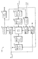
図11には、メモリアレイ112、書き込みワードデコーダ114、書き込みワード線ドライバ116、読み取りワードデコーダ118、読み取りワード線ドライバ120、1つまたは複数のセンス増幅器122、読み取りビットデコーダ124、書き込みビットデコーダ126、書き込みビットドライバ128、比較器130、および出力ドライバ132を備えるメモリ110を示す。これらの要素は複数の線によってともに結合される。例えば、読み取りビットデコーダ124は、複数のアドレス信号からなる列アドレスを受け取る。メモリアレイ112は、トグル動作によりスイッチングすることができるメモリセルのアレイである。メモリアレイ112のメモリセルの一部分が図14に示すメモリアレイ200であり、これは、書き込みが45°の角度の4段階で180°に達するまで行われるという点で、図1のメモリアレイ3について説明した方法で書き込まれるMRAMセルアレイである。この特に好ましいセルアレイにおいて、書き込み動作用と読み取り動作用に別個のワード線およびビット線がある。
11 includes a
読み取りワードデコーダ118は、行アドレスを受け取り、読み取りワード線ドライバ
120に結合され、これがさらにメモリアレイ112に結合される。読み取りのために、読み取りワードデコーダ118が行アドレスに基づいてメモリアレイ112の読み取りワード線を選択する。選択されたワード線は読み取り線ドライバ120によって駆動される。列アドレスを受け取り、センス増幅器122とメモリアレイ112の間に結合される読み取りビットデコーダ124は、読み取りビットデコーダ124から列アドレスに基づいて、メモリアレイ112から読み取りビット線を選択し、これをセンス増幅器122に結合させる。センス増幅器122は、論理状態を検出し、これを出力ドライバ132および比較器130に結合する。出力ドライバ132は、読み取りのために、データ出力信号DOを供給する。書き込み動作のために、比較器130は、センス増幅器122によって供給される選択されたセルの論理状態を、データ入力部(data in )によって供給される書き込むべき所望の論理状態と比較する。
Read
書き込みワードデコーダ114は、行アドレスを受け取り、書き込みワード線ドライバ116に結合され、これがさらにメモリアレイ112に結合される。書き込みのために、書き込みワードデコーダ114は、行アドレスに基づいてメモリアレイ112の書き込みワード線を選択し、次に書き込みワード線ドライバがその選択された書き込みワード線を駆動する。書き込みビットデコーダ126は、列アドレスを受け取り、書き込みビットドライバ128に結合され、これがメモリアレイ112に結合される。書き込みビットデコーダ126は、列アドレスに基づいて書き込みビット線を選択し、次に書き込みビットドライバ128がその選択された書き込みビット線を駆動することにより、選択されたセルの状態をトグルする。
Write
メモリアレイ112はトグルメモリであるため、書き込みトグル動作は、選択されたセルに対して所望の結果として生じる論理状態を達成するためにセルの論理状態をフリップする必要がある場合にのみ完了する。したがって、比較器130は、選択されたセルに対する読み取り動作の出力をセンス増幅器122から受け取り、選択されたセルが既に所望の論理状態を有するかを判定する。行および列アドレスによって決まる選択されたセルが所望の論理状態を有する場合、書き込み動作を終了する。選択されたセルの論理状態が所望の状態と異なる場合、比較器は書き込みビットドライバ128に、書き込みを続けるよう指示し、選択された書き込みビット線用の書き込みビットドライバが、選択された書き込みビット線を駆動する。
Since
図12には、図11のメモリ110の、書き込みワード線WLに結合された書き込みワード線ドライバ116、書き込みビット線BLに結合された書き込みビットドライバ128、および書き込みビット線BLと書き込みワード線WLの交点に結合されたセル134、136、138、および140を含む一部を示す。書き込みを行うには、十分な時間のあいだ、選択された書き込みビット線には電流が流れていない状態で、選択されたワード線WLに電流を供給し、メモリセルの選択された書き込みワード線に沿って第1の角度変化を生じる。選択された書き込みワード線に電流が依然として流れている間に、選択された書き込みビット線に電流を流して、選択されたメモリセルに第2の角度変化を生じる。電流が流れている書き込みビット線と書き込みワード線の交点のみで、この第2の角度変化が生じる。書き込みビット線に電流が依然として流れている間に、選択された書き込みワード線に流れる電流を止め、選択されたメモリセルに第3の角度変化を生じる。選択された書き込みビット線と選択された書き込みワード線の交点のみで、この第3の変化が生じる。選択されたメモリセルの第4の角度変化は、選択された書き込みビット線に流れる電流を止めると生じる。
FIG. 12 shows the write
図13のタイミング図を参照してメモリ110の書き込み動作をさらに説明する。図示のような行または列アドレスの変化により、図13に示すように読み取りワード線WLAをイネーブルすることによって、読み取り動作と書き込みトグル動作の両方が開始される
。論理状態をフリップさせる必要があると判定されるまで書き込みは実行できないが、それでもなお、センス増幅器がその出力を供給し、かつ比較器が論理状態をフリップする必要があるかを判定する前に書き込みワード線がイネーブルされることによって示されるように、書き込みサイクルを開始することができる。書き込みワード線をイネーブルする(書き込みワード線に電流を流す)ことで、選択されたセルならびに選択された書き込みワード線に沿った全てのセルにおいて第1の角度変化が生じるが、書き込みビット線をイネーブルせずに電流を止めた場合、この変化は反転する。
The write operation of the
したがって、単に電流を取り除くことによって第1の角度変化が反転されるため、選択された書き込みワード線は、比較器が判定を行う前にイネーブルされることができる。これは、選択された書き込みワード線上の全てのセルが第1の角度変化を受け、1つを除く全てが選択されないため、当てはまらなければならない。しかし、選択されたセルのみが第2の角度変化を受け、このことは、書き込みビット線がイネーブルされると起こる。これは、論理状態の変化が望ましいという判定を比較器が行った後に起こるものとして示される。第1の角度変化は0°から45°へのものとして示され、第2の変化は45°から90°へのものである。第3の角度変化は、書き込みワード線がディセーブルされる(電流が止まる)と起こるものとして示される。これは、90°から135°へのものとして示される。図示される最後の角度変化は第4の角度変化であり、書き込みビット線がディセーブルされると起こる。この角度変化は135°から180°へのものとして示される。 Thus, the selected write word line can be enabled before the comparator makes a decision because the first angular change is reversed by simply removing the current. This must be true because all cells on the selected write word line have undergone a first angular change and all but one are not selected. However, only the selected cell undergoes a second angular change, which occurs when the write bit line is enabled. This is shown as occurring after the comparator has made the determination that a change in logic state is desirable. The first change in angle is shown as from 0 ° to 45 °, and the second change is from 45 ° to 90 °. The third angular change is shown as occurring when the write word line is disabled (current stops). This is shown as from 90 ° to 135 °. The last angular change shown is the fourth angular change and occurs when the write bit line is disabled. This angular change is shown as from 135 ° to 180 °.
これはまた、別のサイクルを開始させる次のアドレス変化の後に最後の書き込み段階を継続できることを示す。サイクルの開始は、それが書き込みサイクルであっても、常に読み取りとともに開始する。アドレスAがアドレスBに変化し、読み取りワード線Bを選択させる。これは、前に選択されたセルの書き込みを妨害しない。これは読み取りワード線の変化を示すが、アドレスが列のみ変化し、選択された読み取りワード線が変化しない場合でも、継続する電流の流れが書き込みの完了に悪影響を及ぼすことはない。全てのサイクルはいずれにせよ読み取り動作で開始するため、サイクルの開始時に書き込みイネーブルがアクティブである必要はないことにも留意されたい。しかし、書き込みビット線をアクティブにするには、書き込みイネーブル信号が十分早くアクティブでなければならない。 This also indicates that the last write phase can continue after the next address change that initiates another cycle. The start of a cycle always begins with a read, even if it is a write cycle. The address A changes to the address B, and the read word line B is selected. This does not interfere with the writing of previously selected cells. This indicates a change in the read word line, but even if the address changes only in the column and the selected read word line does not change, the continuous current flow does not adversely affect the completion of the write. Note also that the write enable does not need to be active at the beginning of the cycle because every cycle begins with a read operation anyway. However, the write enable signal must be active fast enough to activate the write bit line.
選択されている単一セルに関して説明を行ってきたが、これは理解を容易にするためである。実際には、通常いくつかのセルが選択されることになり、これを図11に、複数の信号線である要素間の信号接続によって示す。したがって、例えば、メモリ110が×16メモリである場合、比較器130は実際には16回の別個の比較を、選択されたセルにつき1回ずつ行う。16回の比較のうち、不一致を示す比較のみが、それらの不一致のある選択されたセルの書き込み動作を生じる。選択されたセルのうち結果的に一致したものはフリップされない。
The description has been given with respect to a single cell being selected for ease of understanding. In practice, several cells will normally be selected, which is illustrated in FIG. 11 by signal connections between elements which are multiple signal lines. Thus, for example, if the
図14には、メモリアレイ200の一部、ならびにまとまってメモリコア201を形成する複数のドライバ、デコーダ、および検知ブロックを示す。このメモリアレイ200の部分は、MRAM装置202、204、206、208、210、212、213、214、216、218、220、222、224、226、227、および228を備える。これらのMRAM装置はそれぞれ3つの電流経路を有する。これら3つの経路のうち、互いに直交するものとして示される第1の電流経路および第2の電流経路は書き込み経路を表す。これらの2つの経路は、図12および図13に示される、セルの論理状態をスイッチングさせる信号を運ぶ。45度の角度の抵抗器として示される第3の電流経路は、2つの可能な抵抗状態の一方にプログラムされる磁気抵抗トンネル接合部を通る読み取り電流経路を表す。メモリアレイ200はさらに、対応するMRAM装置202、204、2
06、208、210、212、213、214、216、218、220、222、224、226、227、および228の読み取り電流経路である第3の電流経路とそれぞれ直列につながれた選択トランジスタ230、232、234、236、238、240、242、244、260、262、264、266、268、270、272、および274を備える。この選択トランジスタの接続は、これらのトランジスタの、第3の電流経路に結合された1つの電流電極と、アース(VSS)に結合された第2の電流電極とにより行われる。選択トランジスタ装置とMRAM装置の各組み合わせがメモリセルを構成する。
FIG. 14 shows a part of the
メモリコア201は、MRAM装置の第1の電流経路を通って延在する書き込みワード線WWL0、WWL1、WWL2、およびWWL3を備える。WWL0は、MRAM装置202、210、216、および224を通って延在する。WWL1は、MRAM装置204、212、218、および226を通って延在する。WWL2は、MRAM装置206、213、220、および227を通って延在する。WWL3は、MRAM装置208、214、222、および228を通って延在する。メモリアレイ200はさらに、MRAM装置の第2の電流経路を通って延在する書き込みビット線WBL0、WBL1、WBL2、およびWBL3を備える。WBL0は、MRAM装置202、204、206、および208を通って延在する。WBL1は、MRAM装置210、212、213、および214を通って延在する。WBL2は、MRAM装置216、218、220、および222を通って延在する。WBL3は、MRAM装置224、226、227、および228を通って延在する。さらになお、メモリアレイ200は、選択トランジスタのゲートに結合される読み取りワード線RWL0、RWL1、RWL2、およびRWL3を備える。RWL0は、選択トランジスタ230、238、260、および268に結合される。RWL1は、選択トランジスタ232、240、262、および270に結合される。RWL2は、選択トランジスタ234、242、264、および272に結合される。RWL3は、選択トランジスタ236、244、266、および274に結合される。メモリアレイ200はまた、読み取りグローバルビット線RGBL0およびRGBL1ならびにグループ選択線GS0、GS1、GS2、およびGS3を備える。
メモリアレイ200はさらに、メモリセルのグループを読み取りグローバルビット線に結合するためのグループ選択トランジスタ250、252、254、256、276、278、280、および282を備える。さらにメモリアレイ200を構成するものとして、ローカルビット線251、253、255、257、277、279、281、および283があり、そのそれぞれが、それらのグループのMRAM装置の第3の電流経路に結合される。つまり、これらのローカルビット線が各グループにつき1本ある。
トランジスタ250および252は、ともに結合されるとともに読み取りグローバルビット線RGBL0に結合された第1の電流電極を有する。トランジスタ254および256は、ともに結合されるとともに読み取りグローバルビット線RGBL0に結合された第1の電流電極を有する。トランジスタ276および278は、ともに結合されるとともに読み取りグローバルビット線RGBL1に結合された第1の電流電極を有する。トランジスタ280および282は、ともに結合されるとともに読み取りグローバルビット線RGBL1に結合された第1の電流電極を有する。トランジスタ250、252、254、256、276、278、280、および282はそれぞれ、ローカルビット線251、253、255、257、277、279、281、および283に結合された第2の電流電極を有する。ローカルビット線251、253、255、257、277、279、281、および283は、MRAM装置202および204、206および208、210および212、213および214、216および218、220および222、224および226、ならびに227および228の第3の電流経路にそれぞれ結合される。グループ選択線GS0はグループ選択トランジスタ250および276に結合される。グル
ープ選択線GS1はグループ選択トランジスタ252および278に結合される。グループ選択線GS2はグループ選択トランジスタ254および280に結合される。グループ選択線GS3はグループ選択トランジスタ256および282に結合される。
メモリアレイ200に加えて、メモリコア201は、書き込み列デコーダ/ドライバ283、284、285、および286、書き込み行デコーダ/ドライバ287、289、291、および293、読み取り行デコーダ/ドライバ288、290、292、および294、ならびに読み取り列デコーダ/センス増幅器295および296を備える。書き込み列デコーダ/ドライバ283、284、285、および286は、書き込みビット線WBL0、WBL1、WBL2、およびWBL3にそれぞれ接続される。書き込み行デコーダ/ドライバ287、289、291、および293は、書き込みワード線WWL0、WWL1、WWL2、およびWWL3にそれぞれ結合される。読み取り行デコーダ/ドライバ288、290、292、および294は、読み取りワード線RWL0、RWL1、RWL2、およびRWL3にそれぞれ結合される。読み取り列デコーダ/センス増幅器296および295は、読み取りグローバルビット線RGBL0およびRGBL1にそれぞれ結合される。
In addition to the
動作中、MRAM装置(例えばMRAM装置202)は、選択された書き込みワード線(例えばWWL0)および選択された書き込みビット線(例えばこの例ではWBL0)に電流を印加して、メモリの状態をトグルすることによって書き込まれる。状態はまた、メモリセルがトグルセルではなく直接書き込みセルである場合、WWL0およびWBL0により直接書き込むこともできる。全てのMRAM装置は、特定のMRAM装置の書き込みワード線および書き込みビット線に電流を流すことによって選択される。MRAM装置(例えばMRAM装置202)の状態は、その対応する選択トランジスタ(例えばトランジスタ230)のゲートに、読み取りワード線RWL0により十分な電圧を印加し、対応するグループトランジスタ(例えばトランジスタ250)のゲートに、グループ選択線GS0により十分な電圧を印加し、選択されたMRAM装置(この例ではMRAM装置202)の状態を、読み取りグローバルビット線RGBL0により、列デコーダ/センス増幅器296によって検知することによって読み取られる。1つのグループは、第3の電流経路を共通して接続された複数のMRAM装置で構成される。よって、セル自体が読み取りグローバルビット線に加える静電容量は、そのグループ内にあるセルに限定される。また、トランジスタ250および252は電流電極が共通して接続されており、ゲートは異なる選択線に結合される。これは、グループを折り返して(fold)グローバルビット線を共有させ、グループ間の選択を別個のグローバル選択線によって達成させる作用をもたらす。したがって、行方向に線が追加されており、列方向のほうが少ない。利点は、行方向における線の増加が各セルグループにつき1本であることである。そのグループが、好ましい量であると考えられる32である場合、セル32個分の距離にさらなるグローバル選択線がある。折り返さない場合、読み取りグローバルビット線が、折り返した場合の2列毎に1本ではなく列毎に1本ある。したがって、折り返さない場合の効果としては、折り返した場合と比較して、セル2つ分の幅の読み取りグローバルビット線が2列毎に1本増える。したがって、このトレードオフは明らかに、折り返したビット線が有利である。この空間的な利点は、線のサイズを大きくして抵抗を減らすため、メモリコアのサイズを小さくするため、あるいはその2つの組み合わせのために用いることができる。
During operation, the MRAM device (eg, MRAM device 202) applies a current to the selected write word line (eg, WWL0) and the selected write bit line (eg, WBL0 in this example) to toggle the state of the memory. Written by. The state can also be written directly by WWL0 and WBL0 if the memory cell is a direct write cell rather than a toggle cell. All MRAM devices are selected by passing current through the write word line and write bit line of a particular MRAM device. The state of an MRAM device (eg, MRAM device 202) is that a sufficient voltage is applied to the gate of its corresponding select transistor (eg, transistor 230) via the read word line RWL0 and the gate of the corresponding group transistor (eg, transistor 250). A sufficient voltage is applied by the group selection line GS0, and the state of the selected MRAM device (in this example, the MRAM device 202) is read by the read global bit line RGBL0 and detected by the column decoder /
さらに、書き込み線を読み取り線と分離することによって、書き込み線の一端を電源VDDに直接接続し、読み取りと書き込みが同一線を共用する場合に必要とされる第2の電流スイッチを排除することができる。したがって、書き込みドライバのための全面積が小さくなり、メモリコアの平均ビットサイズが小さくなる。また、読み取りと書き込みの間で1本の線をスイッチングする必要性をなくすことにより、読み取り回路を損傷する危険性を負うことなく、書き込み電圧を性能について最適化することができる。さらに、選択
トランジスタは書き込み電圧を受け取らないため、これらの選択トランジスタを、書き込みレベルの電圧を受け取らなくてよいことから遥かに小さなサイズにすることができる。これにより、メモリセルのサイズが小さくなる。これは特に、トランジスタを異なる電圧要件に合わせて別々に作製することが一般的である場合に顕著である。
Further, by separating the write line from the read line, one end of the write line is directly connected to the power supply VDD, thereby eliminating the second current switch required when reading and writing share the same line. it can. Therefore, the total area for the write driver is reduced and the average bit size of the memory core is reduced. Also, by eliminating the need to switch a single line between read and write, the write voltage can be optimized for performance without risking damage to the read circuit. Furthermore, since the select transistors do not receive a write voltage, these select transistors can be much smaller in size because they do not need to receive a write level voltage. This reduces the size of the memory cell. This is particularly noticeable when it is common to make transistors separately for different voltage requirements.
図15には、MRAM装置202およびトランジスタ230からなるメモリセルの断面を示す。これは、図14の機構を利用するように構成されたMRAM装置の共通の要素を示す。MRAM技術の通常の応用において、MRAM装置は、拡張ロジックを有する回路(例えばマイクロプロセッサ)上に存在する。このような場合、論理設計に対応する金属階層がいくつかあり、MRAM装置の記憶エレメントは、これらの金属層が形成されてから製造される。これは、通常のトンネル接合部では、劣化することなく約400セルシウス度より高い温度を処理できないことによるものである。
FIG. 15 shows a cross section of a memory cell composed of the
MRAM装置202は、トンネル接合部300、相互接続部306、相互接続部304、ならびに書き込み電流経路314および302を備える。相互接続部304はローカルビット線251でもある。トランジスタ230は、ソース324、ドレイン322、およびゲート323を備える。トランジスタ230のドレイン322は、ロジックとして使用するために金属層として形成される相互接続部318、相互接続部308、相互接続部310、および相互接続部312を介してMRAM装置202に接続される。これらの金属相互接続層は、よく知られているように、バイアを介してともに接続される。書き込み電流経路314は、相互接続部318と同じ金属層に形成される。ゲート323は、相互接続部320に周期的に接続される読み取りワード線RWL0の一部である。相互接続部320の使用により、RWL0の抵抗が小さくなる。これは、ポリシリコンの比較的高い抵抗を防ぐためのよく見られるストラッピング技法である。
The
図16には、図15に示すようなMRAM装置202およびトランジスタ230の断面を示す。この断面は、MRAM装置210およびトランジスタ238を含むように拡張されている。これは、相互接続部310と同じ相互接続階層に読み取りグローバルビット線RGBL0を示す。トンネル接合部300およびWWL0は断面線とずれているため、図16中には存在しないことに留意されたい。図16中に存在するMRAM装置210の部分は書き込みビット線WBL1である。MRAM装置202と同様に、MRAM装置210の第3の電流経路は、相互接続部340、相互接続部338、相互接続部336、相互接続部334、および相互接続部330によってトランジスタ232に接続される。相互接続部330および306はそれぞれ、MRAM装置210および202のトンネル接合部への直接接続を行う。これらの断面は、この機構が、特別な処理を必要とする異常な構造を必要とすることなく作製できることを示す。
FIG. 16 shows a cross section of the
図17には、図14に示すものの代替形態の一部を示す。この場合、各グループのメモリセルは直列メモリとして配置される。隣接ビットセルの複数のグループはそれぞれ、基準電位(reference )に直列接続される。この場合、基準電位はアースである。この代替形態にはローカルビット線がない。同様の特徴に対して同様の装置数が維持される。 FIG. 17 shows a portion of an alternative to that shown in FIG. In this case, the memory cells of each group are arranged as a serial memory. Each group of adjacent bit cells is connected in series to a reference potential. In this case, the reference potential is ground. This alternative has no local bit line. Similar device numbers are maintained for similar features.
例示目的で選択される本明細書中の実施形態に対する様々な変更および修正を当業者であれば容易に思い付くであろう。そのような修正および変形が本発明の精神から逸脱しない範囲において、それらの修正および変形は、添付の特許請求の範囲の公正な解釈のみによって評価される本発明の範囲に含まれることが意図される。 Various changes and modifications to the embodiments herein selected for illustrative purposes will readily occur to those skilled in the art. To the extent that such modifications and variations do not depart from the spirit of the invention, such modifications and variations are intended to be included within the scope of the present invention, which is to be assessed only by a fair interpretation of the appended claims. The
Claims (4)
前記トグルメモリの所定のアドレス位置の読み取り動作を開始するステップ、
前記所定のアドレス位置における書き込みトグル動作の一部を、現在格納されている値に影響を及ぼすことなく開始するステップ、
前記所定のアドレス位置における前記現在格納されているデータ値を、該所定のアドレスに書き込むべき新たな値と比較するステップであって、それによって、該新たな値が前記格納されているデータ値と異なっているか同一であるかを判定する、比較するステップ、および
前記新たな値が前記格納されているデータ値と異なる場合には前記所定のアドレス位置に前記新たな値を書き込むことによって前記書き込みトグル動作を完了し、または前記書き込むべき新たな値が前記格納されているデータ値と同じである場合には前記所定のアドレス位置に前記新たな値を書き込むことなく前記トグル動作を完了するステップ
の一連のステップを備える、トグルメモリの読み取りおよび書き込み方法。A method for reading and writing toggle memory,
Starting a read operation of a predetermined address position of the toggle memory;
Starting a portion of the write toggle operation at the predetermined address location without affecting the currently stored value;
Comparing the currently stored data value at the predetermined address location with a new value to be written to the predetermined address, whereby the new value is compared with the stored data value; Determining and comparing whether they are different or identical; and if the new value is different from the stored data value, writing the new value at the predetermined address location A series of steps to complete the toggle operation without writing the new value to the predetermined address location if the operation is completed or the new value to be written is the same as the stored data value A method for reading and writing a toggle memory comprising the steps of:
前記トグルメモリの所定のアドレス位置において読み取り動作を実施するために必要な第1の時間長を定義するステップ、
前記トグルメモリの前記所定のアドレス位置において書き込み動作を実施するために必要な第2の時間長を定義するステップ、
前記トグルメモリの読み取りワード線ドライバによって前記読み取り動作を開始するステップ、および
前記読み取り動作が完了する前に前記トグルメモリの書き込みビット線ドライバによって前記書き込み動作を開始し、前記所定のアドレス位置が、前記書き込み動作中に書き込みたい書き込み値と同じ情報値を含むと判定された場合に、前記書き込み動作を選択的に終了するステップ
の一連のステップを含む、トグルメモリの読み取りおよび書き込み方法。A method for reading and writing toggle memory,
Defining a first time length required to perform a read operation at a predetermined address location in the toggle memory;
Defining a second time length required to perform a write operation at the predetermined address location of the toggle memory;
Starting the read operation by a read word line driver of the toggle memory; and starting the write operation by a write bit line driver of the toggle memory before the read operation is completed, and the predetermined address position is A toggle memory reading and writing method including a series of steps of selectively terminating the writing operation when it is determined that the same information value as a writing value to be written is included during the writing operation.
列アドレスを受け取って、前記メモリセルのアレイ内の所定のビット列を選択するビット選択信号を前記メモリセルのアレイに供給するビットデコードロジックと、
行アドレスを受け取って、前記メモリセルのアレイ内の所定のビット行を選択するワード選択信号を前記メモリセルのアレイに供給するワードデコードロジックと、
前記メモリセルのアレイに結合され、前記ワードデコードロジックに応答して所定のワード線を駆動する読み取りワード線ドライバと、
前記メモリセルのアレイに結合され、前記ワードデコードロジックおよび書き込みイネーブル信号に応答して所定のワード線を駆動する書き込みワード線ドライバと、
前記ビットデコードロジックに結合され、前記行アドレスおよび列アドレスによって選択されたビットが前記2つの論理状態のどちらを有するかを判定するセンス回路と、
該センス回路に結合され、該センス回路の出力を、前記行アドレスおよび前記列アドレスを含む所定のアドレスに書き込むべき新たな値と比較して、該新たな値が、格納されているデータ値と異なっているか同じであるかを判定する比較器と、
該比較器に結合され、前記書き込みイネーブル信号に応答して前記ビットデコードロジックによって確定される所定の列を駆動し、前記新たな値が前記格納されているデータ値と異なる場合には前記所定のアドレスに前記新たな値を書き込むことによって前記書き込みトグル動作を完了し、前記書き込むべき新たな値が前記格納されているデータ値と同じである場合には前記所定のアドレスに前記新たな値を書き込むことなく前記トグル動作を終了する回路部とを備えるトグルメモリ。An array of memory cells that toggle between two logic states to indicate an information stored value;
Bit decode logic that receives a column address and supplies a bit select signal to the array of memory cells to select a predetermined bit string in the array of memory cells;
Word decode logic that receives a row address and provides a word select signal to the array of memory cells to select a predetermined bit row in the array of memory cells;
A read word line driver coupled to the array of memory cells and driving a predetermined word line in response to the word decode logic;
A write word line driver coupled to the array of memory cells and driving a predetermined word line in response to the word decode logic and a write enable signal;
A sense circuit coupled to the bit decode logic to determine which of the two logic states a bit selected by the row address and column address has;
The output of the sense circuit coupled to the sense circuit is compared with a new value to be written to a predetermined address including the row address and the column address, and the new value is compared with a stored data value. A comparator that determines whether they are different or the same;
Coupled to the comparator, driving a predetermined column determined by the bit decode logic in response to the write enable signal, and the predetermined value if the new value is different from the stored data value The write toggle operation is completed by writing the new value to an address, and the new value is written to the predetermined address if the new value to be written is the same as the stored data value And a circuit unit that terminates the toggle operation without any change.
前記アレイに結合されて、読み取りワード線ドライバによって読み取り動作を開始した後で読み取り動作が完了する前に書き込みビット線ドライバによって書き込み動作を開始することによって前記アレイに情報を書き込む制御回路部であって、書き込みたい新たな値に電流格納値が対応する場合に前記書き込み動作を選択的に終了する制御回路部とを備えるメモリ。An array that stores information by toggling the logical state of the bit position to be written;
A control circuit unit coupled to the array for writing information to the array by starting a write operation by a write bit line driver after a read operation by a read word line driver and before a read operation is completed; And a control circuit unit that selectively terminates the write operation when the current stored value corresponds to a new value to be written.
Applications Claiming Priority (2)
| Application Number | Priority Date | Filing Date | Title |
|---|---|---|---|
| US10/186,141 US6693824B2 (en) | 2002-06-28 | 2002-06-28 | Circuit and method of writing a toggle memory |
| PCT/US2003/013179 WO2004003922A1 (en) | 2002-06-28 | 2003-04-29 | Circuit and method of writing a toggle memory |
Publications (3)
| Publication Number | Publication Date |
|---|---|
| JP2005531876A JP2005531876A (en) | 2005-10-20 |
| JP2005531876A5 JP2005531876A5 (en) | 2006-06-22 |
| JP4359561B2 true JP4359561B2 (en) | 2009-11-04 |
Family
ID=29779824
Family Applications (1)
| Application Number | Title | Priority Date | Filing Date |
|---|---|---|---|
| JP2004517527A Expired - Fee Related JP4359561B2 (en) | 2002-06-28 | 2003-04-29 | Circuit and method for writing to toggle memory |
Country Status (10)
| Country | Link |
|---|---|
| US (1) | US6693824B2 (en) |
| EP (1) | EP1518246B1 (en) |
| JP (1) | JP4359561B2 (en) |
| KR (1) | KR100943112B1 (en) |
| CN (1) | CN100470665C (en) |
| AT (1) | ATE333138T1 (en) |
| AU (1) | AU2003231170A1 (en) |
| DE (1) | DE60306782T2 (en) |
| TW (1) | TWI307887B (en) |
| WO (1) | WO2004003922A1 (en) |
Families Citing this family (18)
| Publication number | Priority date | Publication date | Assignee | Title |
|---|---|---|---|---|
| US6842365B1 (en) * | 2003-09-05 | 2005-01-11 | Freescale Semiconductor, Inc. | Write driver for a magnetoresistive memory |
| US7286378B2 (en) * | 2003-11-04 | 2007-10-23 | Micron Technology, Inc. | Serial transistor-cell array architecture |
| US7613868B2 (en) * | 2004-06-09 | 2009-11-03 | Headway Technologies, Inc. | Method and system for optimizing the number of word line segments in a segmented MRAM array |
| JP2006031795A (en) * | 2004-07-14 | 2006-02-02 | Renesas Technology Corp | Nonvolatile semiconductor memory |
| JP2006065986A (en) * | 2004-08-27 | 2006-03-09 | Fujitsu Ltd | Magnetoresistive memory and magnetoresistive memory writing method |
| JP4012196B2 (en) * | 2004-12-22 | 2007-11-21 | 株式会社東芝 | Data writing method of magnetic random access memory |
| US7543211B2 (en) * | 2005-01-31 | 2009-06-02 | Everspin Technologies, Inc. | Toggle memory burst |
| US7646628B2 (en) * | 2005-02-09 | 2010-01-12 | Nec Corporation | Toggle magnetic random access memory and write method of toggle magnetic random access memory |
| US7630234B2 (en) * | 2005-09-14 | 2009-12-08 | Nec Corporation | Magnetic random access memory |
| US7569902B2 (en) * | 2005-10-28 | 2009-08-04 | Board Of Trustees Of The University Of Alabama | Enhanced toggle-MRAM memory device |
| US7577017B2 (en) * | 2006-01-20 | 2009-08-18 | Industrial Technology Research Institute | High-bandwidth magnetoresistive random access memory devices and methods of operation thereof |
| US7746686B2 (en) * | 2006-04-21 | 2010-06-29 | Honeywell International Inc. | Partitioned random access and read only memory |
| US8111544B2 (en) * | 2009-02-23 | 2012-02-07 | Taiwan Semiconductor Manufacturing Company, Ltd. | Programming MRAM cells using probability write |
| US9613675B2 (en) | 2013-12-14 | 2017-04-04 | Qualcomm Incorporated | System and method to perform low power memory operations |
| WO2016032506A1 (en) * | 2014-08-29 | 2016-03-03 | Siemens Aktiengesellschaft | Controlled convergence compressor flowpath for a gas turbine engine |
| CN204878059U (en) | 2014-12-17 | 2015-12-16 | 依必安-派特穆尔芬根股份有限两合公司 | Blade and fan wheel |
| KR101976045B1 (en) * | 2016-08-30 | 2019-05-09 | 에스케이하이닉스 주식회사 | Magnetic resistance memory device in which state conversion of a data cell is detecable in a write operation and method of performing a read operation and the write operation in the same |
| JP6625278B1 (en) * | 2018-11-22 | 2019-12-25 | 三菱電機株式会社 | I / O control unit, PLC and data control method |
Family Cites Families (14)
| Publication number | Priority date | Publication date | Assignee | Title |
|---|---|---|---|---|
| US4763305A (en) | 1985-11-27 | 1988-08-09 | Motorola, Inc. | Intelligent write in an EEPROM with data and erase check |
| US6256224B1 (en) * | 2000-05-03 | 2001-07-03 | Hewlett-Packard Co | Write circuit for large MRAM arrays |
| US5953248A (en) | 1998-07-20 | 1999-09-14 | Motorola, Inc. | Low switching field magnetic tunneling junction for high density arrays |
| US5946227A (en) | 1998-07-20 | 1999-08-31 | Motorola, Inc. | Magnetoresistive random access memory with shared word and digit lines |
| US6111781A (en) | 1998-08-03 | 2000-08-29 | Motorola, Inc. | Magnetic random access memory array divided into a plurality of memory banks |
| DE19853447A1 (en) * | 1998-11-19 | 2000-05-25 | Siemens Ag | Magnetic storage |
| WO2000042614A1 (en) * | 1999-01-13 | 2000-07-20 | Infineon Technologies Ag | Read/write architecture for a mram |
| US6185143B1 (en) | 2000-02-04 | 2001-02-06 | Hewlett-Packard Company | Magnetic random access memory (MRAM) device including differential sense amplifiers |
| US6191989B1 (en) | 2000-03-07 | 2001-02-20 | International Business Machines Corporation | Current sensing amplifier |
| US6272041B1 (en) | 2000-08-28 | 2001-08-07 | Motorola, Inc. | MTJ MRAM parallel-parallel architecture |
| JP4149647B2 (en) * | 2000-09-28 | 2008-09-10 | 株式会社東芝 | Semiconductor memory device and manufacturing method thereof |
| US6335890B1 (en) | 2000-11-01 | 2002-01-01 | International Business Machines Corporation | Segmented write line architecture for writing magnetic random access memories |
| US6418046B1 (en) * | 2001-01-30 | 2002-07-09 | Motorola, Inc. | MRAM architecture and system |
| DE10107380C1 (en) * | 2001-02-16 | 2002-07-25 | Infineon Technologies Ag | Magnetoresistive memory cell write-in method uses currents supplied to word line and bit line for providing superimposed magnetic fields causing alteration in magnetization direction |
-
2002
- 2002-06-28 US US10/186,141 patent/US6693824B2/en not_active Expired - Fee Related
-
2003
- 2003-04-29 AT AT03724302T patent/ATE333138T1/en not_active IP Right Cessation
- 2003-04-29 AU AU2003231170A patent/AU2003231170A1/en not_active Abandoned
- 2003-04-29 EP EP03724302A patent/EP1518246B1/en not_active Expired - Lifetime
- 2003-04-29 DE DE60306782T patent/DE60306782T2/en not_active Expired - Lifetime
- 2003-04-29 WO PCT/US2003/013179 patent/WO2004003922A1/en active IP Right Grant
- 2003-04-29 KR KR1020047021252A patent/KR100943112B1/en active IP Right Grant
- 2003-04-29 JP JP2004517527A patent/JP4359561B2/en not_active Expired - Fee Related
- 2003-04-29 CN CNB038152959A patent/CN100470665C/en not_active Expired - Fee Related
- 2003-06-26 TW TW092117443A patent/TWI307887B/en not_active IP Right Cessation
Also Published As
| Publication number | Publication date |
|---|---|
| EP1518246A1 (en) | 2005-03-30 |
| ATE333138T1 (en) | 2006-08-15 |
| TWI307887B (en) | 2009-03-21 |
| US20040001352A1 (en) | 2004-01-01 |
| KR100943112B1 (en) | 2010-02-18 |
| TW200409118A (en) | 2004-06-01 |
| AU2003231170A1 (en) | 2004-01-19 |
| CN100470665C (en) | 2009-03-18 |
| EP1518246B1 (en) | 2006-07-12 |
| DE60306782T2 (en) | 2006-11-30 |
| CN1666292A (en) | 2005-09-07 |
| JP2005531876A (en) | 2005-10-20 |
| US6693824B2 (en) | 2004-02-17 |
| DE60306782D1 (en) | 2006-08-24 |
| KR20050009762A (en) | 2005-01-25 |
| WO2004003922A1 (en) | 2004-01-08 |
Similar Documents
| Publication | Publication Date | Title |
|---|---|---|
| US7154772B2 (en) | MRAM architecture with electrically isolated read and write circuitry | |
| JP4359561B2 (en) | Circuit and method for writing to toggle memory | |
| JP4292239B2 (en) | Method for writing to a scalable magnetoresistive random access memory element | |
| US6654278B1 (en) | Magnetoresistance random access memory | |
| US6657889B1 (en) | Memory having write current ramp rate control | |
| JP2003151260A (en) | Thin film magnetic storage device | |
| US6714442B1 (en) | MRAM architecture with a grounded write bit line and electrically isolated read bit line | |
| US6711052B2 (en) | Memory having a precharge circuit and method therefor | |
| US6760266B2 (en) | Sense amplifier and method for performing a read operation in a MRAM | |
| US6714440B2 (en) | Memory architecture with write circuitry and method therefor | |
| KR20100138782A (en) | Memory and write control method | |
| US6744663B2 (en) | Circuit and method for reading a toggle memory cell | |
| JP2002314048A (en) | Ferromagnetic non-volatile memory and refreshing method therefor |
Legal Events
| Date | Code | Title | Description |
|---|---|---|---|
| A521 | Request for written amendment filed |
Free format text: JAPANESE INTERMEDIATE CODE: A523 Effective date: 20060428 |
|
| A621 | Written request for application examination |
Free format text: JAPANESE INTERMEDIATE CODE: A621 Effective date: 20060428 |
|
| A977 | Report on retrieval |
Free format text: JAPANESE INTERMEDIATE CODE: A971007 Effective date: 20090116 |
|
| A131 | Notification of reasons for refusal |
Free format text: JAPANESE INTERMEDIATE CODE: A131 Effective date: 20090210 |
|
| A711 | Notification of change in applicant |
Free format text: JAPANESE INTERMEDIATE CODE: A711 Effective date: 20090224 |
|
| A521 | Request for written amendment filed |
Free format text: JAPANESE INTERMEDIATE CODE: A523 Effective date: 20090508 |
|
| A131 | Notification of reasons for refusal |
Free format text: JAPANESE INTERMEDIATE CODE: A131 Effective date: 20090602 |
|
| A521 | Request for written amendment filed |
Free format text: JAPANESE INTERMEDIATE CODE: A523 Effective date: 20090626 |
|
| TRDD | Decision of grant or rejection written | ||
| A01 | Written decision to grant a patent or to grant a registration (utility model) |
Free format text: JAPANESE INTERMEDIATE CODE: A01 Effective date: 20090721 |
|
| A01 | Written decision to grant a patent or to grant a registration (utility model) |
Free format text: JAPANESE INTERMEDIATE CODE: A01 |
|
| A61 | First payment of annual fees (during grant procedure) |
Free format text: JAPANESE INTERMEDIATE CODE: A61 Effective date: 20090810 |
|
| FPAY | Renewal fee payment (event date is renewal date of database) |
Free format text: PAYMENT UNTIL: 20120814 Year of fee payment: 3 |
|
| R150 | Certificate of patent or registration of utility model |
Free format text: JAPANESE INTERMEDIATE CODE: R150 |
|
| FPAY | Renewal fee payment (event date is renewal date of database) |
Free format text: PAYMENT UNTIL: 20130814 Year of fee payment: 4 |
|
| R250 | Receipt of annual fees |
Free format text: JAPANESE INTERMEDIATE CODE: R250 |
|
| R250 | Receipt of annual fees |
Free format text: JAPANESE INTERMEDIATE CODE: R250 |
|
| LAPS | Cancellation because of no payment of annual fees |