JP4343616B2 - Nanostructure manufacturing method and nanostructure - Google Patents
Nanostructure manufacturing method and nanostructure Download PDFInfo
- Publication number
- JP4343616B2 JP4343616B2 JP2003290538A JP2003290538A JP4343616B2 JP 4343616 B2 JP4343616 B2 JP 4343616B2 JP 2003290538 A JP2003290538 A JP 2003290538A JP 2003290538 A JP2003290538 A JP 2003290538A JP 4343616 B2 JP4343616 B2 JP 4343616B2
- Authority
- JP
- Japan
- Prior art keywords
- substrate
- nanostructure
- thin film
- film
- columnar
- Prior art date
- Legal status (The legal status is an assumption and is not a legal conclusion. Google has not performed a legal analysis and makes no representation as to the accuracy of the status listed.)
- Expired - Fee Related
Links
Images


Landscapes
- Chemically Coating (AREA)
- Physical Vapour Deposition (AREA)
- ing And Chemical Polishing (AREA)
Description
本発明は、無電解めっきによるナノ構造体の製造方法及びそのナノ構造体に関する。 The present invention relates to a method for producing a nanostructure by electroless plating and the nanostructure.
金属及び半導体の薄膜、細線、ドットなどでは、ある特徴的な長さより小さなサイズにおいて、電子の動きが閉じ込められることにより、特異な電気的、光学的、化学的特性を示すことがある。このような観点から、機能性材料として、数十nmより微細なサイズ(幅や厚さなど)をもつ構造を有する材料(以降、「ナノ構造体」)への関心が高まっている。 Metal and semiconductor thin films, thin wires, dots, and the like may exhibit unique electrical, optical, and chemical properties by confining the movement of electrons in a size smaller than a certain characteristic length. From such a viewpoint, as a functional material, there is an increasing interest in a material (hereinafter, “nanostructure”) having a structure having a size (width, thickness, etc.) smaller than several tens of nm.
こうしたナノ構造体の作製方法としては、例えば、フォトリソグラフィーをはじめ、電子線露光、X線露光などの微細パターン形成技術をはじめとする半導体加工技術によって直接的にナノ構造体を作製する方法が挙げられる。 As a method for producing such a nanostructure, for example, a method for directly producing a nanostructure by a semiconductor processing technique including a fine pattern forming technique such as photolithography, electron beam exposure, and X-ray exposure is given. It is done.
また、前記ナノ構造体の作製方法のほかに、自然に形成される規則的な構造、すなわち自己規則的に形成される構造あるいは自己形成的に作製される方法もある。これらの手法は、ベースとして用いる微細構造によっては、従来の方法を上まわる微細で特殊な構造を作製できる可能性があるため、多くの研究が行われはじめている。このような自己規則的あるいは自己形成的手法として、ナノサイズの細孔を有するナノ構造体を制御よく大面積に形成できる陽極酸化が挙げられる(特許文献1参照)。たとえば、アルミニウムを酸性浴中で陽極酸化することで作製する陽極酸化アルミナが知られている。 In addition to the method for producing the nanostructure, there is also a regular structure that is naturally formed, that is, a self-regularly formed structure or a self-formed method. Many of these techniques are being studied because there is a possibility that a fine and special structure can be produced over the conventional method depending on the fine structure used as a base. As such a self-regular or self-forming method, anodization capable of forming a nanostructure having nano-sized pores in a large area with good control can be mentioned (see Patent Document 1). For example, anodized alumina prepared by anodizing aluminum in an acidic bath is known.
また、無電解めっき法については、基体の材質及びその形状の如何を問わず、均一厚さで且つ均質な薄膜が得られる特徴を持っているので、機能性の高い成膜技術として電子材料分野で広く利用されている。無電解めっきに用いる金属としては、Cu、Ni、Coが比較的利用され、また、Au、Pd、Pt、Agなどの貴金属も最近利用されることが多くなってきた。例えば、銅めっきは電子工業におけるプリント配線基板のスルーホールめっき、ニッケルめっきは装飾、耐食、耐磨耗を目的とした表面処理技術として利用されている。また、最近Ni、Co等を主体とした無電解めっき膜の持つ特性そのものを利用する機能めっきの応用としては、抵抗体、電極、配線、磁気記録媒体などが実用化されている(特許文献2参照)。
上述したような無電解めっきは、めっき液に浸すという簡易な方法で薄膜を形成することが可能であり、電極や配線などの微細構造の高機能性化は進んでいる。特に、数十nm以上数μm以下のサイズを有する構造体の高機能性化または高密度化が進んでいるが、数十nm以下のサイズを有する微細構造を形成するのが困難である。 In the electroless plating as described above, a thin film can be formed by a simple method of immersing in a plating solution, and high functionality of a fine structure such as an electrode or a wiring has been advanced. In particular, a structure having a size of several tens of nanometers to several μm or less is increasing in functionality or density, but it is difficult to form a fine structure having a size of several tens of nanometers or less.
本発明は、このような従来の事情を考慮してなされたもので、無電解めっきによる高機能性化を図り、数十nm以下のサイズを有する微細構造を形成することができるナノ構造体の製造方法を提供するものである。 The present invention has been made in view of such conventional circumstances, and is intended to increase the functionality by electroless plating and to form a nanostructure capable of forming a fine structure having a size of several tens of nanometers or less. A manufacturing method is provided.
本発明は、基板、下地膜、SiまたはGeを主材料とした薄膜、前記薄膜の細孔中に形成された柱状構造体からなるナノ構造体の製造方法において、前記下地膜付きの基板と、前記基板表面に形成されたAlを主成分とする柱状部材と、前記Alを主成分とする柱状部材の側面を囲むように配置されるSi、Ge、SiGeのいずれかを主成分とするマトリックスからなる構造体を有するAl(Si,Ge)混合薄膜を形成した基体中の前記Alを主成分とする柱状部材を除去することにより前記基体中に細孔を形成する工程と、無電解めっき浴に前記細孔を形成した基体を浸すことにより前記細孔中に柱状構造体を形成する工程とを含むことを特徴とする。 The present invention relates to a substrate, a base film, a thin film mainly composed of Si or Ge, and a nanostructure manufacturing method including a columnar structure formed in the pores of the thin film. A columnar member mainly composed of Al formed on the surface of the substrate and a matrix mainly composed of any one of Si, Ge, and SiGe disposed so as to surround the side surface of the columnar member mainly composed of Al. A step of forming pores in the substrate by removing the columnar member mainly composed of Al in the substrate on which the Al (Si, Ge) mixed thin film having the structure is formed, and an electroless plating bath Forming a columnar structure in the pores by immersing the substrate on which the pores are formed.
前記柱状部材は、前記基板に対して垂直又は略垂直方向に形成されることが好ましい。 The columnar member is preferably formed in a direction perpendicular or substantially perpendicular to the substrate.
また、前記ナノ構造体の製造方法において、前記基体中に細孔を形成する工程は、無電解めっき浴に浸すことにより、前記基体中の前記Alを主成分とする柱状部材を除去すると同時に細孔を形成するものが好ましい。 In the method for producing a nanostructure, the step of forming pores in the substrate may be performed by immersing the substrate in an electroless plating bath to simultaneously remove the columnar member mainly composed of Al in the substrate. Those that form holes are preferred.
また、前記ナノ構造体の製造方法において、前記下地膜は、触媒活性を有してもよい。前記触媒活性を有する下地膜は、PdまたはPd合金であってもよい。 In the method for manufacturing a nanostructure, the base film may have catalytic activity. The base film having catalytic activity may be Pd or a Pd alloy.
また、前記ナノ構造体の製造方法において、前記マトリックスは、(Si,Al)OX混合薄膜(0≦X≦2)、(Ge,Al)OX混合薄膜(0≦X≦2)、(Si,Ge,Al)OX混合薄膜(0≦X≦2)のいずれかであってもよい。 Further, in the method for producing a nanostructure, the matrix includes (Si, Al) O x mixed thin film (0 ≦ X ≦ 2), (Ge, Al) O x mixed thin film (0 ≦ X ≦ 2), ( Any of Si, Ge, Al) O x mixed thin films (0 ≦ X ≦ 2) may be used.
また、前記ナノ構造体の製造方法において、前記柱状構造体は、金属、酸化物のいずれかであってもよい。前記金属は、Co、Ni、Pt、Pdの少なくとも1種類以上であってもよい。前記柱状構造体の金属材料として、少量のB、Pのいずれかを含んでもよい。前記酸化物は、ZnOであってもよい。 In the method for manufacturing a nanostructure, the columnar structure may be a metal or an oxide. The metal may be at least one of Co, Ni, Pt, and Pd. A small amount of either B or P may be included as the metal material of the columnar structure. The oxide may be ZnO.
本発明におけるナノ構造体の製造方法では、基体を無電解めっき浴に浸すことにより、その基体の有する細孔中に柱状構造体を形成することができる。 In the method for producing a nanostructure in the present invention, a columnar structure can be formed in the pores of the substrate by immersing the substrate in an electroless plating bath.
本発明によれば、基体を無電解めっき浴に浸すことにより、前記基体中の細孔に金属、酸化物のいずれかである柱状構造体を形成するナノ構造体の製造方法を提供することができる。 According to the present invention, it is possible to provide a method for producing a nanostructure in which a columnar structure that is either a metal or an oxide is formed in pores in the substrate by immersing the substrate in an electroless plating bath. it can.
また、本発明によれば、低コストで容易且つ大面積に柱状構造体を形成するナノ構造体の製造方法を提供することができる。さらに、本発明によれば、金属である柱状構造体を形成したナノ構造体を用いることで電極、配線などの高機能化されたナノデバイスを提供することが可能である。また、本発明により磁性体である柱状構造体を形成したナノ構造体を用いた磁気デバイスを提供することができる。さらに、本発明により、発光素子、光電変換素子、光触媒素子などのZnO柱状構造体を形成したナノ構造体を用いた光デバイスを提供することができる。 In addition, according to the present invention, it is possible to provide a method for manufacturing a nanostructure that can easily form a columnar structure in a large area at low cost. Furthermore, according to the present invention, it is possible to provide a highly functional nanodevice such as an electrode or a wiring by using a nanostructure formed with a columnar structure that is a metal. Moreover, the magnetic device using the nanostructure which formed the columnar structure which is a magnetic body by this invention can be provided. Furthermore, the present invention can provide an optical device using a nanostructure formed with a ZnO columnar structure such as a light emitting element, a photoelectric conversion element, and a photocatalytic element.
以下、本発明に係るナノ構造体を実施するための最良の形態について添付図面を用いて詳しく説明する。
(本発明におけるナノ構造体について)
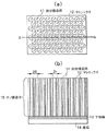
図1は、本発明におけるナノ構造体の構成の一例を示す概略図を示す。図1(a)及び(b)において、11は柱状構造体、12はSi、Ge、SiGeのいずれかを主成分とするマトリックス(マトリックス部分)、13は下地膜(下地層)、14は基板、15はナノ構造体である。
Hereinafter, the best mode for carrying out the nanostructure according to the present invention will be described in detail with reference to the accompanying drawings.
(Nanostructure in the present invention)
FIG. 1 is a schematic view showing an example of the configuration of a nanostructure in the present invention. In FIGS. 1A and 1B, 11 is a columnar structure, 12 is a matrix (matrix portion) containing Si, Ge, or SiGe as a main component, 13 is a base film (base layer), and 14 is a substrate. , 15 are nanostructures.
ナノ構造体15は、図1(a)及び(b)に示すように、基板14上に形成された下地膜13の表面上に、該基板14の表面に対して垂直又は略垂直方向に形成された多数の柱状構造体11と、この柱状構造体11の側面を取り囲むように配置され、Si、Ge、SiGeのいずれかを主成分とするマトリックス12とを有し、マトリックス12中に多数の柱状構造体11が分散している。
As shown in FIGS. 1A and 1B, the nanostructure 15 is formed on the surface of the
柱状構造体11は、Pt、Pd、CoP、CoB、CoNiP、NiP、NiBなどの金属、及びZnOなどの酸化物のいずれかから構成される。柱状構造体11の直径(平面形状が円の場合は直径)2r(図1(b)参照)は、主としてナノ構造体15の製造条件により制御することが可能であるが、その平均直径は20nm以下、好ましくは1nm以上15nm以下である。なお、楕円等の場合は、最も長い外径部の範囲内であればよい。ここで平均直径とは、例えば、実際のSEM写真で観察される柱状の部分を、その写真から直接、あるいはコンピュータで画像処理して、導出される値である。なお、薄膜をどのようなデバイスに用いるか、あるいはどのような処理を行うかにもよるが、平均径の下限としては1nm以上、あるいは数nm以上であることが実用的な下限値である。また、柱状構造体11間の中心間距離2R(図1(b)参照)は、30nm以下、好ましくは5nm以上20nm以下である。
The columnar structure 11 is made of any one of metals such as Pt, Pd, CoP, CoB, CoNiP, NiP, and NiB, and oxides such as ZnO. The diameter of the columnar structure 11 (diameter when the planar shape is a circle) 2r (see FIG. 1B) can be controlled mainly by the manufacturing conditions of the nanostructure 15, but the average diameter is 20 nm. Hereinafter, it is preferably 1 nm or more and 15 nm or less. In the case of an ellipse or the like, it may be within the range of the longest outer diameter portion. Here, the average diameter is a value derived from, for example, a columnar portion observed in an actual SEM photograph, either directly from the photograph or by image processing with a computer. Although it depends on what device the thin film is used for and what kind of treatment is performed, the practical lower limit is that the lower limit of the average diameter is 1 nm or more, or several nm or more. The
ナノ構造体15は、膜状の構造体であることが好ましく、柱状構造体11は、下地膜13及び基板14に対して垂直又は略垂直になるようにマトリックス12中に分散していることが好ましい。ナノ構造体15を成す膜状の構造体の膜厚としては、特に限定されるものではないが、1nm〜100μmの範囲で適用できる。プロセス時間等を考慮してより現実的な膜厚としては、1nm〜1μm程度である。
(Al(Si,Ge)混合薄膜の構造体について)
図2は、ナノ構造体15の基になるAl(Si,Ge)混合薄膜の概略図を示す。図2(a)及び(b)において、21は柱状部材、22はSi、Ge、SiGeのいずれかを主成分とするマトリックス(マトリックス部分)、23は基板、24はAl(Si,Ge)混合薄膜である。Al(Si,Ge)混合薄膜24は、SiまたはGeからなっている材料中にAlを成分にした多数の柱状部材21が下地膜付きの基板23に対して垂直又は略垂直方向に形成する構造体を有する薄膜である。以下、その構造体について詳述する。
The nanostructure 15 is preferably a film-like structure, and the columnar structures 11 are dispersed in the matrix 12 so as to be perpendicular or substantially perpendicular to the
(Al (Si, Ge) mixed thin film structure)
FIG. 2 is a schematic view of an Al (Si, Ge) mixed thin film on which the nanostructure 15 is based. 2 (a) and 2 (b), 21 is a columnar member, 22 is a matrix (matrix portion) containing Si, Ge, or SiGe as a main component, 23 is a substrate, and 24 is Al (Si, Ge) mixed. It is a thin film. The Al (Si, Ge) mixed
Al(Si,Ge)混合薄膜24は、(Si,Al)OX混合薄膜(0≦X≦2)、(Ge,Al)OX混合薄膜(0≦X≦2)、及び(Si,Ge,Al)OX混合薄膜(0≦X≦2)のいずれかで構成される。
The Al (Si, Ge) mixed
ここでは、Al(Si,Ge)混合薄膜24として、(Si,Al)OX混合薄膜(0≦X≦2)について説明するが、このうち、X=0の(Al,Si)混合薄膜24を用いる。
Here, an (Si, Al) O x mixed thin film (0 ≦ X ≦ 2) will be described as the Al (Si, Ge) mixed
この混合薄膜24は、Alを主成分とする柱状部材21が、Siを主成分として構成される領域つまりマトリックス22に取り囲まれている。この混合薄膜24には、Siが、AlとSiの全量に対して20at%以上70at%以下の割合で含まれている。この割合は、混合薄膜24を構成するAlとSiの全量に対するSiの割合のことであり、好ましくは25at%以上65at%以下、より好ましくは30at%以上60at%以下である。上記のAlとSiの割合を示すat%とは、SiとAlの原子の数の割合を示し、atom%あるいはat%とも記載され、例えば誘導結合型プラズマ発光分析法(ICP法)で(Al,Si)混合薄膜24中のSiとAlの量を定量分析したときの値である。
In this mixed
なお、実質的に柱状形状が実現していればよく、例えば柱状部材21に部材の成分としてSiが含まれていてもよいし、柱状部材21以外の領域つまりマトリックス22にAlが含まれていてもよい。また、柱状部材21やその周囲の領域に酸素、アルゴン、窒素、水素などが含まれていてもよい。
The columnar shape may be substantially realized. For example, the
また、(Al,Ge)混合薄膜、(Al,Si,Ge)混合薄膜の場合も同様にして、(Al,Si)混合薄膜の場合に前述したSiの代わりにそれぞれGe、SiGeを用いて適用できる。 Similarly, in the case of the (Al, Ge) mixed thin film and the (Al, Si, Ge) mixed thin film, Ge and SiGe are used instead of Si as described above in the case of the (Al, Si) mixed thin film. it can.
また、混合薄膜24には、Alを「A材料」、Si、Ge、及びSiGeのいずれかを「B材料」として、A、B材料の両方の成分系相平衡図において、共晶点を有する材料(いわゆる共晶系の材料)を用いている。特に共晶点が300℃以上好ましくは400℃以上であるのがよい。なお、A材料とB材料との好ましい組み合わせとしては、A材料としてAlを用い、B材料としてSiを用いる形態、A材料としてAlを用い、B材料としてGeを用いる形態、あるいはA材料としてAlを用い、B材料としてSiyGe1-y(0<y<1)を用いるのが好ましい。
Further, the mixed
また、柱状部材21を囲むマトリックス22は、非晶質であることが望ましい。また、柱状部材21の平面形状としては円形あるいは楕円形状である。
The
混合薄膜24には、前記B材料を含み構成されるマトリックス22中に複数の前記柱状部材21が分散していることになる。柱状部材21の径(平面形状が円の場合は直径)は、主として混合薄膜24の組成(即ち、前記B材料の割合)に応じて制御可能であるが、その平均直径は、20nm以下、好ましくは1nm以上15nm以下である。なお、楕円等の場合は、最も長い外径部の範囲内であればよい。ここで平均直径とは、例えば、実際のSEM写真で観察される柱状の部分を、その写真から直接、あるいはコンピュータで画像処理して、導出される値である。なお、混合薄膜24をどのようなデバイスに用いるか、あるいはどのような処理を行うかにもよるが、平均直径の下限としては1nm以上、あるいは数nm以上であることが実用的な下限値である。
In the mixed
また、複数の柱状部材21間の中心間距離2R(図2)は、30nm以下、好ましくは5nm以上20nm以下である。
The
混合薄膜24は、膜状の構造体であることが好ましく、柱状部材21は基板23に対して垂直になるように前記B材料を含み構成されるマトリックス22中に分散していることが好ましい。混合薄膜24の膜厚としては、特に限定されるものではないが、1nm〜100μmの範囲で適用できる。プロセス時間等を考慮して、現実的な膜厚としては、1nm〜1μm程度が好ましい。
(本発明におけるナノ構造体の製造方法について)
次に、本発明におけるナノ構造体の製造方法について詳細に説明する。
The mixed
(About the manufacturing method of the nanostructure in this invention)
Next, the manufacturing method of the nanostructure in this invention is demonstrated in detail.
図3は、本発明におけるナノ構造体の製造方法の一実施態様を示す工程図を示す。本発明における製造方法は、下地膜13を形成した基板14上に混合薄膜24(一例として(Si,Al)OX混合薄膜(0≦X≦2)を採用する。)を形成し、この混合薄膜24の有する細孔31中に前記基板14上に垂直方向に柱状構造体33を形成するもので、下記の(a)工程〜(d)工程を有することを特徴とする。
FIG. 3 is a process chart showing one embodiment of a method for producing a nanostructure in the present invention. In the manufacturing method according to the present invention, a mixed thin film 24 (an (Si, Al) O x mixed thin film (0 ≦ X ≦ 2) is adopted as an example) is formed on a
(a)工程(図3(a)参照)
まず、基板14上に下地膜13を形成する。本工程では、触媒活性を有する基板14を用いてもよい。
(A) Process (refer FIG. 3 (a))
First, the
(b)工程(図3(b)参照)
次に、AlとSiを非平衡状態で物質を形成する成膜法を用いて、前記(a)工程で作製した基板14上に(Al,Si)混合薄膜24を形成する(ここでは(Si,Al)OX混合薄膜24(X=0))。
(B) Process (refer FIG.3 (b))
Next, an (Al, Si) mixed
成膜された(Al,Si)混合薄膜24は、Alを主成分とする柱状部材21と前記柱状部材21を囲むSiを主成分とするマトリックス22とを有し、AlとSiの全量に対してSiを20at%以上70at%以下の割合で含有する構造体からなる。
The formed (Al, Si) mixed
(c)工程((図3(c)参照))
次に、(Al,Si)混合薄膜24のAlのみを選択的にエッチングして細孔31を形成する。この(Al,Si)混合薄膜24に対し、Siに比べてAlを溶かしやすい酸あるいはアルカリを用いたウエットエッチングを施すと、Alを主成分とする柱状部材21からAlがエッチングされて細孔31が形成されて、(Si,Al)OX多孔質体32(0<X≦2)が形成される。
(C) Process ((refer FIG.3 (c)))
Next, only the Al of the (Al, Si) mixed
(d)工程(図3(d)参照)
次に、前記(b)工程で作製した(Al,Si)混合薄膜24または前記(c)工程で作製した(Si,Al)OX多孔質体32(0<X≦2)の細孔31中に無電解めっきにより柱状構造体33を充填させ、本発明のナノ構造体34を形成する。
(D) Process (refer FIG.3 (d))
Next, the (Al, Si) mixed
なお、上記では混合薄膜24として(Si,Al)OX混合薄膜(0≦X≦2)を採用した場合の製造方法を説明しているが、その他、(Ge,Al)OX混合薄膜(0≦X≦2)、(Si,Ge,Al)OX混合薄膜(0≦X≦2)の製造方法については、Siの代わりにGe、SiGeを用いる以外は、前述した(Si,Al)OX混合薄膜(0≦X≦2)の場合と同様に以上の(a)工程〜(d)工程を有することを特徴とする。 In the above as a mixed film 24 (Si, Al) O X mixed film describes a manufacturing method of (0 ≦ X ≦ 2) when adopted, but other, (Ge, Al) O X mixed thin film ( 0 ≦ X ≦ 2), (Si, Ge, Al) O x mixed thin film (0 ≦ X ≦ 2) is manufactured as described above (Si, Al) except that Ge and SiGe are used instead of Si. Similar to the case of the O x mixed thin film (0 ≦ X ≦ 2), the above-described steps (a) to (d) are included.
ナノ構造体34は、非平衡状態で成膜する方法を利用して作製することができる。本発明における成膜方法としては、スパッタリング法が好ましいが、抵抗加熱蒸着、電子ビーム蒸着(EB蒸着)、イオンプレーティング法をはじめとする任意の非平衡状態で物質を形成する成膜法が適用可能である。スパッタリング法で行う場合には、マグネトロンスパッタリング、RFスパッタリング、ECRスパッタリング、DCスパッタリング法を用いることができる。 The nanostructure 34 can be manufactured using a method of forming a film in a non-equilibrium state. As a film forming method in the present invention, a sputtering method is preferable, but a film forming method for forming a material in any non-equilibrium state such as resistance heating evaporation, electron beam evaporation (EB evaporation), or ion plating method is applied. Is possible. When the sputtering method is used, magnetron sputtering, RF sputtering, ECR sputtering, or DC sputtering can be used.
次に、一例として、本発明の(Si,Al)OX混合薄膜(0≦X≦2)24を用いた場合のナノ構造体の製造方法を以下の(a)〜(d)の順に追って説明する。 Next, as an example, the manufacturing method of the nanostructure in the case of using the (Si, Al) O x mixed thin film (0 ≦ X ≦ 2) 24 of the present invention is followed in the order of the following (a) to (d). explain.
(a)工程:下地膜の形成工程
無電解めっきを行うには、基板14上に触媒活性を有する下地膜13を形成する必要がある。前記触媒としては、Pd、Pt、Cu、Ag、Au、Rh、Irなどの貴金属元素などが好ましい。また、単体だけでなく二種類以上の金属を混合させた合金膜を用いてもよく、合金膜の組成比を所望通りに制御してもよい。また、本発明においては、Pdは触媒活性がとても優れていることから、特に、Pd単体及びPd合金を用いることが好ましい。触媒活性を有する膜を選択的に形成することで選択的に無電解めっき皮膜を形成させることが可能であるが、特に平坦性を有した連続した膜が好ましい。また、1層以上の微粒子膜を用いてもよい。また、膜厚も所望通りに制御してもよいが、100nm以下が好ましい。特に20nm以下が好ましい。触媒活性を有する下地膜13の形成方法として、ゾルゲル法、蒸着法、スパッタリング法などが挙げられるが、本発明においてはスパッタリング法を採用し、膜厚20nm以下の触媒活性を有する連続した膜を形成する。
(A) Process: Formation process of base film In order to perform electroless plating, it is necessary to form the
(b)工程:(Al,Si)混合薄膜(ここでは(Si,Al)OX混合薄膜(X=0))の形成工程
次に、(a)工程で作製した基板14上に(Al,Si)混合薄膜24を形成する。ここでは、非平衡状態で物質を形成する成膜法として、スパッタリング法を用いた例を説明する。
(B) Process: (Al, Si) mixed thin film (here, (Si, Al) O x mixed thin film (X = 0)) forming process Next, (Al, Si) is formed on the
基板上に、非平衡状態で物質を形成する成膜法であるマグネトロンスパッタリング法により、(Al,Si)混合薄膜24を形成する。(Al,Si)混合薄膜24は、Alを主成分とする柱状部材21と、その周囲のSiを主成分とするマトリックス22から構成される。
An (Al, Si) mixed
なお、図4において、41は基板、42はArプラズマ、43はSiチップ(Si又はGeチップ)、44はAlのスパッタリングターゲットである。スパッタリング法を用いる場合は、AlとSiの割合を簡単に変化させることができる。 In FIG. 4, 41 is a substrate, 42 is Ar plasma, 43 is a Si chip (Si or Ge chip), and 44 is a sputtering target of Al. When the sputtering method is used, the ratio of Al and Si can be easily changed.
図4に示すように、非平衡状態で物質を形成する成膜法であるマグネトロンスパッタリング法により、反応装置内で、Siチップ43を配置したAlターゲット44上に放電用ガスとして導入されたArガスによる高密度のArプラズマ42を発生させ、そのプラズマ62中のArイオンを、Siチップ43を配置したAlターゲット44に衝突させてそのイオン衝撃でSi及びAlをはじき出し、基板41上にそのSi及びAlの混合体からなる(Al,Si)混合薄膜24を形成する。
As shown in FIG. 4, Ar gas introduced as a discharge gas onto an
原料としてのSi及びAlは、図4に示すようにAlのターゲット44上にSiチップ43を配することで達成される。また、図4に示すように、Siチップ43は複数に分けて配置しているが、勿論これに限定されるものではなく、所望の成膜が可能であれば、1つであってもよい。但し、均一なAlを含む柱状部材21をSiを主成分とするマトリックス22領域内に均一に分散させるには、Alターゲット44上にSiチップ43を対称に配置しておくのがよい。また、所定量のAlとSiとの粉末を焼成して作製したAlSi焼成物を成膜のターゲット材として用いることもできる。また、AlターゲットとSiターゲットを別々に用意し、同時に両方のターゲットをスパッタリングする方法を用いてもよい。
As shown in FIG. 4, Si and Al as raw materials can be achieved by arranging a Si chip 43 on an
形成される膜中のシリコンの量は、AlとSiの全量に対して20〜70at%であり、好ましくは25〜65at%、さらに好ましくは30〜60at%である。Si量が斯かる範囲内であれば、Siを主成分とするマトリックス22領域内にAlを主成分とする柱状部材21が分散した(Al,Si)混合薄膜24が得られる。
The amount of silicon in the film to be formed is 20 to 70 at%, preferably 25 to 65 at%, more preferably 30 to 60 at%, based on the total amount of Al and Si. If the amount of Si is within such a range, the (Al, Si) mixed
上記の様にして成膜された(Al,Si)混合薄膜24は、Alを主成分とする柱状部材21と、その周囲のSiを主成分とするマトリックス22領域とを備える。
The (Al, Si) mixed
Alを主成分とする柱状部材21の組成は、柱状構造の微細構造体が得られていれば、シリコン、水素、酸素、アルゴン、窒素などの他の元素を含有していてもよい。
The composition of the
また、Alを主成分とする柱状部材21の周囲を囲んでいるマトリックス22領域の組成は、Siを主成分とするが、柱状構造の微細構造体が得られていれば、アルミニウム、酸素、アルゴン、窒素、水素などの各種の元素を含有してもよい。
Further, the composition of the
また、基板41の温度としては、300℃以下であり、好ましくは200℃以下であるのがよい。 In addition, the temperature of the substrate 41 is 300 ° C. or lower, preferably 200 ° C. or lower.
なお、このような方法で(Al,Si)混合薄膜24を形成すると、AlとSiが準安定状態の共晶型組織となり、AlがSiマトリックス22内に数nmレベルのナノ構造体(柱状部材21)を形成し、自己組織的に分離する。そのときのAlはほぼ円柱状形状であり、その孔径は1〜15nmであり、中心間距離は2nm以上30nm以下である。
When the (Al, Si) mixed
(Al,Si)混合薄膜24のSiの量は、例えばAlターゲット44上に置くSiチップ43の量を変えることで制御できる。また、非平衡状態で成膜を行う場合、特にスパッタリング法の場合は、Arガスを流したときの反応装置内の圧力は、0.2〜1Pa程度が好ましい。また、プラズマを形成するための出力は4インチターゲットでは、150〜1000W程度が好ましい。しかし、特に、これに限定されるものではなく、Arプラズマ42が安定に形成される圧力及び出力で成膜を行えばよい。
The amount of Si in the (Al, Si) mixed
基板14としては、例えば石英ガラスやプラスチックをはじめとする絶縁体基板、シリコンやガリウム砒素をはじめとする半導体基板、金属基板、または、これらの基板の上に1層以上の絶縁体、半導体、金属のいずれかの膜を形成したものが挙げられる。なお、(Al,Si)混合薄膜24の形成に不都合がなければ、基板の材質、厚さ、機械的強度などは特に限定されるものではない。また、基板の形状としては平滑な板状のものに限らず、曲面を有するもの、表面にある程度の凹凸や段差を有するものなどが挙げられるが、(Al,Si)混合薄膜24に不都合がなければ、特に限定されるものではない。
As the
また、(Al,Ge)混合薄膜、(Al,Si,Ge)混合薄膜も同様にして、上述した(Al,Si)混合薄膜の場合に用いたSiの代わりにそれぞれGe、SiGeを用いれば適用できる。 Similarly, the (Al, Ge) mixed thin film and the (Al, Si, Ge) mixed thin film can be similarly applied if Ge and SiGe are used instead of Si used in the case of the (Al, Si) mixed thin film described above. it can.
(c)工程:細孔形成工程
上記の(Al,Si)混合薄膜24中のAl領域(Alを主成分とする柱状部材21領域)のみを選択的にエッチングを行う。その結果、(Al,Si)混合薄膜24には、細孔31を有するSiを主成分とするマトリックス22領域のみが残るが、エッチングを行う度に(Al,Si)混合薄膜24は酸化される場合があるので、(Si,Al)OX多孔質体32(0≦X≦2)が形成されることにする。なお、(Si,Al)OX多孔質体32(0≦X≦2)の細孔31は、中心間距離2Rが30nm以下、平均直径2rが20nm以下であるが、好ましくは、細孔31の平均直径2rは1nm〜15nmであり、その中心間距離2Rは5nm〜20nmである。また、長さは0.5nm〜数μm、好ましくは1nm〜1000nmの範囲である。
(C) Process: Pore forming process Only the Al region (the
エッチングに用いる溶液は、例えばAlを溶かしSiはほとんど溶解しない、りん酸、硫酸、塩酸、クロム酸溶液などの酸が挙げられるが、エッチングによる細孔形成に不都合がなければ水酸化ナトリウムやアンモニア水などのアルカリを用いることができ、特に酸の種類やアルカリの種類に限定されるものではない。また、数種類の酸溶液やあるいは数種類のアルカリ溶液を混合したものを用いてもかまわない。またエッチング条件は、例えば、溶液温度、濃度、時間などは、作製する(Si,Al)OX多孔質体32(0≦X≦2)に応じて、適宜設定することができる。また、(Al,Ge)混合薄膜24、(Al,Si,Ge)混合薄膜24も同様にして、上述した(Al,Si)混合薄膜24の場合に用いたSiの代わりにそれぞれGe、SiGeを用いれば適用できる。
Examples of the solution used for etching include acids such as phosphoric acid, sulfuric acid, hydrochloric acid, and chromic acid solution in which Al is dissolved and Si is hardly dissolved. However, if there is no problem in forming pores by etching, sodium hydroxide or aqueous ammonia is used. An alkali such as, for example, can be used, and is not particularly limited to the type of acid or the type of alkali. Also, a mixture of several types of acid solutions or several types of alkali solutions may be used. Etching conditions can be set as appropriate according to the (Si, Al) O x porous body 32 (0 ≦ X ≦ 2) to be produced, for example, the solution temperature, concentration, and time. Similarly, the (Al, Ge) mixed
(d)工程:(b)工程で作製した(Al,Si)混合薄膜24または(c)工程で作製した(Si,Al)OX多孔質体32(0≦X≦2)の細孔31中に無電解めっきにより柱状構造体33を充填させ、本発明のナノ構造体34を形成する工程
本発明における無電解めっきにより作製する柱状構造体33の材料としては、Ni、Coの鉄族金属、Au、Pd、Pt、Agなどの貴金属、ZnOなどの酸化物が用いられるのが好ましいが、V、Mo、W、Mn、Re、Fe、Zn、Tl、B、C、N、Pなどの少量の不純物を含有してもよい。例えば、CoP、CoB、CoNiP、CoFeP、CoZnP、CoNiMnPなどである。また、抵抗体、電極、配線、磁気記録媒体などの小型化、高密度化などのように、本発明における(Al,Si)OX多孔質体32(0≦X≦2)の細孔31中に前記柱状構造体33を充填することで、前記柱状構造体33の有する高機能性が発揮される。先述したような材料であれば、目的に応じてどの材料を用いてもよい。
Step (d): (Al, Si) mixed
本発明における柱状構造体33の製造方法として、無電解めっき液に(c)工程で作製した(Si,Al)OX多孔質体(0≦X≦2)32及び下地膜13付きの基板14を浸すことで、前記(Si,Al)OX多孔質体32(0≦X≦2)の細孔31中に柱状構造体33を形成させることが可能である。
As a manufacturing method of the columnar structure 33 in the present invention, the (Si, Al) O x porous body (0 ≦ X ≦ 2) 32 and the
無電解めっきに用いるめっき液の主成分としては、析出させる金属を含む塩つまり金属塩、ヒドラジン、次亜リン酸ナトリウム、ジメチルアミンボランなどの金属イオンを金属として析出させるために電子を与える還元剤がある。また、めっき浴に金属の沈殿を生じさせないようにするのに必要な添加剤、つまり錯化剤もある。クエン酸ナトリウムや酒石酸ナトリウムなどの錯化剤を添加することにより金属イオンを金属錯体にしてそのままの状態にすることが可能なので、錯化剤も添加するのが好ましい。また、水酸化ナトリウムやアンモニア水などの塩基性化合物などのpH調整剤は、めっき速度、還元効率及びめっき皮膜の状態に大きく及ぼすが、無電解めっき液のpHを安定させるためにpH調整剤を添加するのが好ましい。無電解めっき液のpHは、無電解めっきの種類によって色々と違うが、無電解めっき液のpHは(Si,Al)OX多孔質体32(0≦X≦2)が高速で溶けない程度の範囲内であれば、酸性またはアルカリ性を有する無電解めっき液を用いてもよい。 The main component of the plating solution used for electroless plating is a reducing agent that gives electrons to deposit metal ions such as salts containing metal to be deposited, that is, metal salts, hydrazine, sodium hypophosphite, dimethylamine borane, etc. There is. There are also additives, i.e. complexing agents, necessary to prevent metal precipitation in the plating bath. The addition of a complexing agent such as sodium citrate or sodium tartrate makes it possible to convert the metal ion into a metal complex and leave it as it is, so it is also preferable to add a complexing agent. In addition, pH adjusters such as basic compounds such as sodium hydroxide and aqueous ammonia greatly affect the plating rate, reduction efficiency, and the state of the plating film, but in order to stabilize the pH of the electroless plating solution, a pH adjuster is used. It is preferable to add. The pH of the electroless plating solution varies depending on the type of electroless plating, but the pH of the electroless plating solution is such that (Si, Al) O x porous body 32 (0 ≦ X ≦ 2) does not dissolve at high speed. If it is in the range, an electroless plating solution having acidity or alkalinity may be used.
無電解めっきによる柱状構造体33の作製条件として、金属塩、還元剤、錯化剤、pH調整剤などのめっき浴における成分の種類の組み合わせ、各々の濃度、めっき液温度、攪拌速度、pHの調整、基板を無電解めっき液に浸す時間が挙げられるが、これらを制御することで所望通りのサイズを有する柱状構造体33を作製することが可能である。 As the preparation conditions of the columnar structure 33 by electroless plating, combinations of the types of components in the plating bath such as metal salt, reducing agent, complexing agent, pH adjusting agent, each concentration, plating solution temperature, stirring speed, pH The adjustment and the time for immersing the substrate in the electroless plating solution can be mentioned. By controlling these, the columnar structure 33 having a desired size can be produced.
また、(b)工程で作製した(Al,Si)混合薄膜24を無電解めっき液に浸すことにより、酸化されて形成した(Si,Al)OX多孔質体32(0≦X≦2)の細孔31中に柱状構造体33を形成する方法については、無電解めっき液に(Al,Si)混合薄膜24を浸す間に、Siを主成分とするマトリックス22を溶解させずにAlを主成分とする柱状部材21を下地膜13表面の位置まで溶解させて(Al,Si)混合薄膜24に細孔31をあけることで、(Si,Al)OX多孔質体32(0≦X≦2)を形成する必要がある。つまり、無電解めっきに用いるめっき液は、Siを主成分とするマトリックス22が変化しないもしくは酸化する程度、もしくは少し溶ける程度、且つAlを主成分とする柱状部材21が溶ける程度のpHの範囲を有することが好ましい。特に、pH3以上pH6以下の酸性、またはpH10以上pH12以下のアルカリ性であることが好ましい。金属塩、還元剤、錯化剤、pH調整剤などのめっき浴における成分の種類の組み合わせ、各々の濃度、めっき液温度、攪拌速度、pHの調整、基板を無電解めっき液に浸す時間の制御によって、Alを主成分とする柱状部材21の溶かし具合を制御することが可能である。攪拌速度や無電解めっき液に基板を浸す時間などを調整することで、Alを主成分とする柱状部材21を全て溶解させることにより細孔31を形成させる。続いて、前記基板を前記無電解めっき液に浸した状態のままで、前記細孔31中に柱状構造体33を形成すればよい。また、(Al,Ge)混合薄膜、(Al,Si,Ge)混合薄膜も同様にして、上述した(Al,Si)混合薄膜の場合に用いたSiの代わりにそれぞれGe、SiGeを用いれば適用できる。
Further, the (Si, Al) O x porous body 32 (0 ≦ X ≦ 2) formed by oxidation by immersing the (Al, Si) mixed
以下、実施例を用いて本発明を更に説明する。 The present invention will be further described below using examples.
本実施例は、一例として、(Al,Si)混合薄膜24を形成した下地Pd膜13付きのSi基板14をエッチングした後、前記基板14を白金無電解めっき液に浸すことによりナノ構造体34を作製した例について説明する(図3参照)。
In this embodiment, as an example, after the
まず、触媒活性を有する下地膜13として、スパッタリング法によりSi基板14上に膜厚20nmのPd薄膜を形成した(図3(a)参照)。さらに、下地Pd膜13付きのSi基板14上にスパッタリング法により膜厚100nmのAl:Siの組成比が3:2であることを有する(Al,Si)混合薄膜24を形成した(図3(b)参照)。
First, as the
前記基板の表面をFE−SEM(電界放出走査型電子顕微鏡)で観察した結果、直径が約5nm、中心間距離が約10nmであるAlを主成分とする柱状部材21がSiを主成分とするマトリックス22の表面中に多数出来ていた(図2(a)参照)。また、断面の観察した結果、Alを主成分とする柱状部材21は下地膜13付きのSi基板23に対して垂直方向に形成されていた(図2(b)参照)。以後、これを「基体」とする。
As a result of observing the surface of the substrate with a FE-SEM (Field Emission Scanning Electron Microscope), the
次いで、前記基体を25℃に設定したリン酸5wt%中に6時間浸すことでエッチングを行った。この試料をFE−SEMで断面観察した結果、Alを主成分とする柱状部材21は全て溶解されて直径が約5nm、中心間距離が約10nmである細孔31が形成されていた(図3(c)参照)。
Next, etching was performed by immersing the substrate in 5 wt% phosphoric acid set at 25 ° C. for 6 hours. As a result of cross-sectional observation of this sample by FE-SEM, all the
次に、白金無電解めっき液の作製方法として、100mLのレクトロレスPt100基本液(日本エレクトロプレイティング・エンジニヤース(株))、10mLのアンモニア水28%、2mLのレクトロレスPt100還元剤(日本エレクトロプレイティング・エンジニヤース(株))、88mLの純水を混合させて白金無電解めっき液を作製した。前記めっき液のpHは12となっていた。 Next, as a method for preparing a platinum electroless plating solution, 100 mL of Rectoless Pt100 basic solution (Nippon Electroplating Engineers Co., Ltd.), 10 mL of ammonia water 28%, 2 mL of Rectoles Pt100 reducing agent (Nippon Electroplating) -Engineers Co., Ltd.) and 88 mL of pure water were mixed to prepare a platinum electroless plating solution. The pH of the plating solution was 12.
続いて、前記白金無電解めっき液を加熱して60℃に設定した。この状態で前記基体を前記めっき液に30分間浸した。この試料をFE−SEMで観察した結果、前基体中のAlを主成分とする柱状部材21が溶解されてできた細孔31中に白金柱状構造体33が形成されていた(図3(d)参照)。この白金柱状構造体33は、直径が約5nmで、高さは約100nmとなっていた。また、中心間距離は約10nmであった。
Subsequently, the platinum electroless plating solution was heated to 60 ° C. In this state, the substrate was immersed in the plating solution for 30 minutes. As a result of observing this sample with an FE-SEM, a platinum columnar structure 33 was formed in the pore 31 formed by dissolving the
上述したように、AlとSiとの組成比、膜厚を制御して形成した(Al,Si)混合薄膜24のAlを主成分とする柱状部材21をエッチングしてから、白金無電解めっき液に浸すことで、前記エッチングにより形成された細孔31中に白金柱状構造体33を形成することが可能である。また、エッチング液の種類の選択、エッチング時間、エッチング液の温度、攪拌速度、エッチング液のpHを制御することで、所望通りAlを主成分とする柱状部材21の溶かし具合を制御することが可能である。
As described above, after etching the
本実施例は、一例として、(Al,Si)混合薄膜24を形成した下地Pd膜13付きのSi基板14をエッチングした後、その基板14をパラジウム無電解めっき液に浸すことによりナノ構造体34を作製した例について説明する(図3参照)。
In the present embodiment, as an example, after the
まず、触媒活性を有する下地膜13として、スパッタリング法によりSi基板14上に膜厚20nmのPd薄膜を形成した(図3(a)参照)。さらに、下地Pd膜13付きのSi基板14上にスパッタリング法により膜厚100nmのAl:Siの組成比が3:2であることを有する(Al,Si)混合薄膜24を形成した(図3(b)参照)。
First, as the
前記基板の表面をFE−SEMで観察した結果、直径が5nm、中心間距離が10nmであることを有するAlを主成分とする柱状部材21がSiを主成分とするマトリックス22表面中に多数出来ていた(図2(a)参照)。また、断面の観察した結果、Alを主成分とする柱状部材21は下地膜13付きのSi基板23に対して垂直方向に形成されていた(図2(b)参照)。以後、これを「基体」とする。
As a result of observing the surface of the substrate with FE-SEM, a large number of
また、前記基体を25℃に設定したリン酸5wt%中に6時間浸すことでエッチングを行った。この試料をFE−SEMで断面観察した結果、Alを主成分とする柱状部材21は全て溶解されて直径が約5nm、中心間距離が約10nmである細孔31が形成されていた(図3(c)参照)。
Etching was performed by immersing the substrate in 5 wt% phosphoric acid set at 25 ° C. for 6 hours. As a result of cross-sectional observation of this sample by FE-SEM, all the
次に、パラジウム無電解めっき液の作製方法として、0.01mol/lの塩化パラジウム、0.08mol/lのエチレンジアミン、0.02mol/lの亜リン酸ナトリウム、30mg/lのチオジグリコール酸を混合させてパラジウム無電解めっき液を作製した。前記めっき液のpHは7となっていた。続いて、前記パラジウム無電解めっき液を加熱して50℃に設定した。この状態で前記基体を前記めっき液に30分間浸した。 Next, as a method for preparing a palladium electroless plating solution, 0.01 mol / l palladium chloride, 0.08 mol / l ethylenediamine, 0.02 mol / l sodium phosphite, 30 mg / l thiodiglycolic acid were used. A palladium electroless plating solution was prepared by mixing. The pH of the plating solution was 7. Subsequently, the palladium electroless plating solution was heated and set to 50 ° C. In this state, the substrate was immersed in the plating solution for 30 minutes.
この試料をFE−SEMで観察した結果、前基体中のAlを主成分とする柱状部材21が溶解されてできた細孔31中にPを少量含有したPdP柱状構造体33が形成されていた(図3(d)参照)。この柱状構造体33は、直径が約5nmで、高さは約80nmとなっていた。また、中心間距離は約10nmであった。
As a result of observing this sample with an FE-SEM, a PdP columnar structure 33 containing a small amount of P was formed in the pores 31 formed by dissolving the
上述したように、AlとSiとの組成比、膜厚を制御して形成した(Al,Si)混合薄膜24のAlを主成分とする柱状部材21をエッチングしてから、パラジウム無電解めっき液に浸すことで、前記エッチングにより形成された細孔31中にPdP柱状構造体33を形成することが可能である。また、エッチング液の種類の選択、エッチング時間、エッチング液の温度、攪拌速度、エッチング液のpHを制御することで、所望通りAlの柱状部材21の溶かし具合を制御することが可能である。
As described above, after etching the
本実施例は、一例として、(Al,Si)混合薄膜24を形成した下地Pd膜13付きのSi基板14を白金無電解めっき液に浸すことによりナノ構造体34を作製した例について説明する(図3(a)、(b)、及び(d)参照)。
In this embodiment, as an example, an example in which the nanostructure 34 is produced by immersing the
まず、触媒活性を有する下地膜13として、スパッタリング法によりSi基板14上に膜厚20nmのPd薄膜を形成した(図3(a)参照)。さらに、下地Pd膜13付きのSi基板14上にスパッタリング法により膜厚100nmのAl:Siの組成比が3:2であることを有する(Al,Si)混合薄膜24を形成する(図3(b)参照)。以後、これを「基体」とする。
First, as the
前記基体の表面をFE−SEMで観察した結果、直径が約5nm、中心間距離が約10nmであることを有するAlを主成分とする柱状部材21がSiを主成分とするマトリックス22表面中に多数できていた(図2(a)参照)。また、断面の観察した結果、Alを主成分とする柱状部材21はSi基板14に対して下地Pd膜13から垂直方向に形成されていた(図2(b)参照)。
As a result of observing the surface of the substrate by FE-SEM, the
次に、白金無電解めっき液の作製方法として、100mLのレクトロレスPt100基本液(日本エレクトロプレイティング・エンジニヤース(株))、10mLのアンモニア水28%、2mLのレクトロレスPt100還元剤(日本エレクトロプレイティング・エンジニヤース(株))、88mLの純水を混合させて白金無電解めっき液を作製した。前記めっき液のpHは12となっていた。 Next, as a method for preparing a platinum electroless plating solution, 100 mL of Rectoless Pt100 basic solution (Nippon Electroplating Engineers Co., Ltd.), 10 mL of ammonia water 28%, 2 mL of Rectoles Pt100 reducing agent (Nippon Electroplating) -Engineers Co., Ltd.) and 88 mL of pure water were mixed to prepare a platinum electroless plating solution. The pH of the plating solution was 12.
続いて、前記白金無電解めっき液を加熱して60℃に設定した。この状態で前記基体を前記めっき液に1時間浸した。この試料をFE−SEMで観察した結果、前基体中のAlを主成分とする針状部材21部分が溶解されて出来た細孔31中に白金柱状構造体33が形成されていた。この白金柱状構造体33は、直径が約5nmで、高さは約100nmとなっていた。また、中心間距離は約10nmであった(図3(d)参照)。
Subsequently, the platinum electroless plating solution was heated to 60 ° C. In this state, the substrate was immersed in the plating solution for 1 hour. As a result of observing this sample with an FE-SEM, a platinum columnar structure 33 was formed in the pores 31 formed by dissolving the portion of the needle-
また、上述したように、AlとSiとの組成比、膜厚を制御して形成した(Al,Si)混合薄膜24の膜厚に合わせて、白金無電解めっき液に浸す時間、めっき液のpH、めっき液の温度、攪拌速度を制御することで、所望通りのサイズを有する白金柱状構造体33を形成することが可能である。また、白金以外の金属の無電解めっきを行う場合でも同様に所望通りのサイズを有するナノ構造体34を形成することも可能である。
Further, as described above, according to the film thickness of the (Al, Si) mixed
本実施例は、一例として、(Al,Si)混合薄膜を形成した下地Pd合金膜13付きのSi基板14を白金無電解めっき液に浸すことによりナノ構造体34を作製した例について説明する(図3参照)。
In this embodiment, as an example, an example in which the nanostructure 34 is produced by immersing the
まず、触媒活性を有する下地膜13にPd合金膜を用いることにして、Pd以外の金属としてPtを選択し、スパッタリング法によりSi基板14上に膜厚20nmの下地Pd合金膜を形成した。Pd:Ptの組成比として、2:1、1:1、1:2の組成比を含有している3種類の下地Pd合金薄膜を形成した(図3(a)参照)。さらに、スパッタリング法により、前記3種類の下地Pd合金薄膜付きのSi基板14上に、膜厚100nmのAl:Siの組成比が3:2であることを有する(Al,Si)混合薄膜24を形成した(図3(b)参照)。以後、これらを「基体」とする。
First, a Pd alloy film was used for the
前記基体の表面をFE−SEMで観察した結果、全ての基体は、直径が約5nm、中心間距離が約10nmであることを有するAlを主成分とする柱状部材21がSiを主成分とするマトリックス22表面中に多数できていた(図2(a)参照)。また、前記基体の断面を観察した結果、Alを主成分とする柱状部材21はSi基板14に対して下地Pd合金膜から垂直方向に形成されていた(図2(b)参照)。
As a result of observing the surface of the substrate with an FE-SEM, all the substrates have a
次に、白金無電解めっき液の作製方法として、100mLのレクトロレスPt100基本液(日本エレクトロプレイティング・エンジニヤース(株))、10mLのアンモニア水28%、2mLのレクトロレスPt100還元剤(日本エレクトロプレイティング・エンジニヤース(株))、88mLの純水を混合させて白金無電解めっき液を作製した。前記めっき液のpHは12となっていた。 Next, as a method for preparing a platinum electroless plating solution, 100 mL of Rectoless Pt100 basic solution (Nippon Electroplating Engineers Co., Ltd.), 10 mL of ammonia water 28%, 2 mL of Rectoles Pt100 reducing agent (Nippon Electroplating) -Engineers Co., Ltd.) and 88 mL of pure water were mixed to prepare a platinum electroless plating solution. The pH of the plating solution was 12.
続いて、前記白金無電解めっき液を加熱して60℃に設定した。この状態で前記基体を前記めっき液に1時間浸した。この試料をFE−SEMで観察した結果、全ての基体は前記基体中のAlを主成分とする柱状部材21の部分が溶解されてできた細孔31中に白金柱状構造体33が形成されていた。
Subsequently, the platinum electroless plating solution was heated to 60 ° C. In this state, the substrate was immersed in the plating solution for 1 hour. As a result of observing this sample with an FE-SEM, as for all the substrates, platinum columnar structures 33 are formed in the pores 31 formed by dissolving the portion of the
Pd:Ptの組成比が2:1、1:1、1:2である3種類の下地Pd合金薄膜上において、全て白金柱状構造体33が得られ、それぞれの直径は全て約5nmであった。また、中心間距離は約10nmであった(図3(d)参照)。 Platinum columnar structures 33 were obtained on the three types of underlying Pd alloy thin films having Pd: Pt composition ratios of 2: 1, 1: 1, and 1: 2, and their respective diameters were all about 5 nm. . The center-to-center distance was about 10 nm (see FIG. 3 (d)).
上述したように、下地Pd合金薄膜中のPd:Ptの組成比を変えても白金柱状構造体33を形成することが可能である。 As described above, the platinum columnar structure 33 can be formed even if the composition ratio of Pd: Pt in the underlying Pd alloy thin film is changed.
本実施例は、一例として、(Al,Ge)混合薄膜24を形成した下地Pd膜13付きのSi基板14を白金無電解めっき液に浸すことによりナノ構造体33を作製した例について説明する(図3参照)。
In this embodiment, as an example, an example in which the nanostructure 33 is produced by immersing the
例えば、下地Pd薄膜付き(膜厚20nm)のSi基板33上にスパッタリング法により膜厚100nmのAl:Geの組成比が3:2であることを有する(Al,Ge)混合薄膜32を形成する(図3(b)参照)。以後、これを「基体」とする。 For example, an (Al, Ge) mixed thin film 32 having an Al: Ge composition ratio of 3: 2 is formed by sputtering on a Si substrate 33 with a base Pd thin film (film thickness 20 nm) by sputtering. (See FIG. 3B). Hereinafter, this is referred to as “substrate”.
前記基体の表面をFE−SEMで観察した結果、実施例1と同様に直径が約10nm、中心間距離が約15nmであることを有するAlを主成分とする柱状部材21がGeを主成分とするマトリックス22表面中に多数できていた(図2(a)参照)。また、前記基体の断面を観察した結果、Alを主成分とする柱状部材21はSi基板14に対して下地Pd膜13から垂直方向に形成されていた(図2(b)参照)。
As a result of observing the surface of the substrate with FE-SEM, as in Example 1, the
次に、白金無電解めっき液の作製方法として、100mLのレクトロレスPt100基本液(日本エレクトロプレイティング・エンジニヤース(株))、10mLのアンモニア水28%、2mLのレクトロレスPt100還元剤(日本エレクトロプレイティング・エンジニヤース(株))、88mLの純水を混合させて白金無電解めっき液を作製した。前記めっき液のpHは12となっていた。 Next, as a method for preparing a platinum electroless plating solution, 100 mL of Rectoless Pt100 basic solution (Nippon Electroplating Engineers Co., Ltd.), 10 mL of ammonia water 28%, 2 mL of Rectoles Pt100 reducing agent (Nippon Electroplating) -Engineers Co., Ltd.) and 88 mL of pure water were mixed to prepare a platinum electroless plating solution. The pH of the plating solution was 12.
続いて、前記白金無電解めっき液を加熱して60℃に設定した。この状態で前記基体を前記めっき液に1時間浸した。この試料をFE−SEMで観察した結果、前基体中のAlを主成分とする柱状部材21の部分が溶解されてできた細孔31中に白金柱状構造体33が形成されていた。この白金柱状構造体33は、直径が約10nmで、高さは約70nmとなっていた。また、中心間距離は約15nmとなっていた(図3(d)参照)。
Subsequently, the platinum electroless plating solution was heated to 60 ° C. In this state, the substrate was immersed in the plating solution for 1 hour. As a result of observing this sample with an FE-SEM, a platinum columnar structure 33 was formed in the pore 31 formed by dissolving the portion of the
また、上述したように、AlとGeとの組成比、膜厚を制御して形成した(Al,Ge)混合薄膜24の膜厚に合わせて、白金無電解めっき液に浸す時間、めっき液のpH、めっき液温度、攪拌速度を制御することで、所望通りのサイズを有する白金柱状構造体33を形成したナノ構造体34を形成することが可能である。また、白金以外の金属の無電解めっきを行う場合でも同様に所望通りのサイズを有するナノ構造体34を形成することも可能である。
Further, as described above, according to the film thickness of the (Al, Ge) mixed
また、(Al,Si,Ge)混合薄膜の場合も同様に、Al、Si、Geとの組成比、膜厚を制御して形成した(Al,Si,Ge)混合薄膜24の膜厚に合わせて、白金無電解めっき液に浸す時間、めっき液のpH、めっき液温度、攪拌速度を制御することで、所望通りのサイズを有する白金柱状構造体33を形成したナノ構造体34を形成することが可能である。また、白金以外の金属、酸化物の無電解めっきを行う場合でも同様に所望通りのサイズを有するナノ構造体34を形成することも可能である。
Similarly, in the case of the (Al, Si, Ge) mixed thin film, the thickness is adjusted to the thickness of the (Al, Si, Ge) mixed
本実施例は、一例として、(Al,Si)混合薄膜24を形成した下地Pd膜13付きのSi基板14をエッチングした後、前記基板14をCoNiB無電解めっき液に浸すことによりナノ構造体34を作製した例について説明する(図3参照)。
In this embodiment, as an example, after etching the
例えば、下地Pd膜13付き(膜厚20nm)のSi基板14上にスパッタリング法により膜厚が100nm、Al:Siの原子量の比が3:2である(Al,Si)混合薄膜24を形成する(図3(b)参照)。以後、これを「基体」とする。
For example, a (Al, Si) mixed
前記基体の表面をFE−SEMで観察した結果、直径が約5nm、中心間距離が約10nmであることを有するAlを主成分とする柱状部材21がSiを主成分とするマトリックス22表面中に多数出来ていた(図2(a)参照)。また、前記基体の断面を観察した結果、Alを主成分とする柱状部材21はSi基板14に対して下地Pd膜13から垂直方向に形成されていた(図2(b)参照)。
As a result of observing the surface of the substrate by FE-SEM, the
次いで、前記基体を25℃に設定したリン酸5wt%中に6時間浸すことでエッチングを行った。このFE−SEMで断面観察した結果、Alを主成分とする柱状部材21は全て溶解されて直径が約5nm、中心間距離が約10nmである細孔31が形成されていた(図3(c)参照)。
Next, etching was performed by immersing the substrate in 5 wt% phosphoric acid set at 25 ° C. for 6 hours. As a result of cross-sectional observation with this FE-SEM, all the
次に、CoNiB無電解めっき液の作製方法として、0.03mol/lの硫酸コバルト、0.07mol/lの硫酸ニッケル、0.2mol/lの次亜リン酸ナトリウム、0.2mol/lのクエン酸ナトリウム、0.5 mol/lのホウ砂を混合させて、CoNiB無電解めっき液を作製した。さらに、水酸化ナトリウムの添加により前記無電解めっき液のpHは7に設定した。前記無電解めっき液を加熱して90℃に設定した。この状態で前記基体を前記めっき液に30分間浸した。 Next, a CoNiB electroless plating solution was prepared by using 0.03 mol / l cobalt sulfate, 0.07 mol / l nickel sulfate, 0.2 mol / l sodium hypophosphite, 0.2 mol / l quencher. Sodium niobate and 0.5 mol / l borax were mixed to prepare a CoNiB electroless plating solution. Furthermore, the pH of the electroless plating solution was set to 7 by adding sodium hydroxide. The electroless plating solution was heated to 90 ° C. In this state, the substrate was immersed in the plating solution for 30 minutes.
この試料をFE−SEMで観察した結果、前基体中のAlを主成分とする柱状部材21部分が溶解されてできた細孔31中にCoNiB柱状構造体33が形成されていた(図3(d)参照)。前記柱状構造体33は直径が約5nmで、高さは約100nmとなっていた。また、中心間距離は約10nmであった。
As a result of observing this sample with an FE-SEM, CoNiB columnar structures 33 were formed in the pores 31 formed by dissolving the
また、前記CoNiB柱状構造体33に磁場を印加し測定した結果、垂直磁気異方性のある強磁性特性を示していたので、高密度化された垂直磁気記録媒体として用いた磁気デバイスを提供することが可能である。 Further, as a result of applying and measuring a magnetic field to the CoNiB columnar structure 33, the ferromagnetic characteristics having perpendicular magnetic anisotropy were shown. Therefore, a magnetic device used as a high-density perpendicular magnetic recording medium is provided. It is possible.
上述したように、CoNiBやCoNiPなどの二種類以上の金属を混合させた柱状構造体33をAl(Si,Ge)混合薄膜24の形成された細孔31中に無電解めっきで形成することが可能なので、上述したようなナノ構造体34は磁気デバイスを提供することが可能である。
As described above, the columnar structure 33 in which two or more kinds of metals such as CoNiB and CoNiP are mixed may be formed by electroless plating in the pores 31 in which the Al (Si, Ge) mixed
本実施例は、一例として、(Al,Si)混合薄膜24を形成した下地Pd膜13付きのガラス基板14をエッチングした後、その基板14をZnO無電解めっき液に浸すことによりナノ構造体34を作製した例について説明する(図3参照)。
In this embodiment, as an example, after etching the
例えば、下地Pd膜13付き(膜厚5nm)のSi基板14上にスパッタリング法により膜厚100nmのAl:Siの原子量の比が3:2であることを有する(Al,Si)混合薄膜24を形成する(図3(b)参照)。以後、これを「基体」とする。
For example, an (Al, Si) mixed
前記基体の表面をFE−SEMで観察した結果、直径が約5nm、中心間距離が約10nmである事を有するAlを主成分とする柱状部材21がSiを主成分とするマトリックス22表面中に多数できていた(図2(a)参照)。また、前記基体の断面を観察した結果、Alを主成分とする柱状部材21はガラス基板14に対して下地Pd膜13から垂直方向に形成されていた(図2(b)参照)。
As a result of observing the surface of the substrate by FE-SEM, the
次いで、前記基体を25℃に設定したリン酸5wt%中に6時間浸すことでエッチングを行った。この試料をFE−SEMで断面観察した結果、Alを主成分とする柱状部材21は全て溶解されて直径が約5nm、中心間距離が約10nmである細孔31が形成されていた(図3(c)参照)。
Next, etching was performed by immersing the substrate in 5 wt% phosphoric acid set at 25 ° C. for 6 hours. As a result of cross-sectional observation of this sample by FE-SEM, all the
次に、ZnO無電解めっき液の作製方法として、0.05mol/lの硝酸亜鉛、0.05mol/lのジメニルアミンボランを混合させて、ZnO無電解めっき液を作製した。前記無電解めっき液を加熱して65℃に設定した。この状態で前記基体を前記めっき液に40分間浸した。 Next, as a method for producing a ZnO electroless plating solution, 0.05 mol / l zinc nitrate and 0.05 mol / l dimethylenylborane were mixed to produce a ZnO electroless plating solution. The electroless plating solution was heated and set to 65 ° C. In this state, the substrate was immersed in the plating solution for 40 minutes.
この試料をFE−SEMで観察した結果、前基体中のAlを主成分とする柱状部材21部分が溶解されてできた細孔31中にZnO柱状構造体33が形成されていた(図3(d)参照)。この柱状構造体33は、直径が約5nmで、高さは約90nmとなっていた。また、中心間距離は約10nmであった。
As a result of observing this sample with an FE-SEM, ZnO columnar structures 33 were formed in the pores 31 formed by dissolving the
また、前記基体をHe−Cdレーザーを励起源としたフォトルミネッセンスの測定を行った結果、前記基体より波長385nm付近のバンド間発光と波長500nm〜550nm付近の緑色発光を確認できたので、前記基体を発光素子として用いることが可能である。 Further, as a result of measuring the photoluminescence using the He—Cd laser as an excitation source for the substrate, it was confirmed that interband emission near a wavelength of 385 nm and green emission near a wavelength of 500 nm to 550 nm were confirmed from the substrate. Can be used as a light-emitting element.
上述したように、ZnO柱状構造体33をAl(Si,Ge)混合薄膜24の細孔31中に無電解めっきで形成することが可能なので、上述したようなナノ構造体34を用いることで発光素子、光電変換素子、光触媒素子などの機能性を発揮できる光デバイスを提供することが可能である。
As described above, since the ZnO columnar structure 33 can be formed by electroless plating in the pores 31 of the Al (Si, Ge) mixed
次に、本発明によるナノ構造体の製造方法で用いるAl(Si,Ge)混合薄膜の構造体(図2、図3(b)の混合薄膜24参照)に関する予備実験について説明する。この構造体は、第1の材料としてAl、第2の材料としてSi、Geの少なくとも1種類以上の元素を主成分とするマトリックス部を含むが、ここでは第2の材料としてSiを用いている。
(実験例1:第1の材料Al、第2の材料Si)
Siに周囲を囲まれたAl構造体部分が円柱状構造であり、径2rが3nmであり、間隔2Rが7nm、長さLが200nmであるAl細線(図2、図3(b)の柱状部材21参照)について説明する。
Next, a preliminary experiment on an Al (Si, Ge) mixed thin film structure (see the mixed
(Experimental example 1: first material Al, second material Si)
The Al structure part surrounded by Si is a columnar structure, the
まず、Al細線の作製方法を説明する。 First, a method for producing an Al thin wire will be described.
ガラス基板上に、RFマグネトロンスパッタリング法を用いて、SiをAlとSiの全量に対して55atomic%含んだAlSi混合膜を約200nm形成する。ターゲットには、4インチのAlターゲット上に15mm角のSiチップ13を8枚おいたものを用いた。スパッタ条件は、RF電源を用いて、Ar流量:50sccm、放電圧力:0.7Pa、投入電力:1kWとした。また、基板温度は室温とした。 An AlSi mixed film containing Si at 55 atomic% with respect to the total amount of Al and Si is formed on a glass substrate by using an RF magnetron sputtering method. The target used was 8 pieces of 15 mm square Si chips 13 on a 4-inch Al target. Sputtering conditions were as follows: using an RF power source, Ar flow rate: 50 sccm, discharge pressure: 0.7 Pa, and input power: 1 kW. The substrate temperature was room temperature.
なお、ここではターゲットとして、Alターゲット上にSiチップを8枚置いたものを用いたが、Siチップの枚数はこれに限定されるものではなく、スパッタ条件により変化し、AlSi混合膜の組成が約55atomic%近辺になれば良い。また、ターゲットはAlターゲット上にSiチップを置いたものに限定したものではなく、Siターゲット上にAlチップを置いたものでも良いし、SiとAlの粉末を焼結したターゲットを用いても良い。 In this case, the target used was eight Si chips placed on an Al target. However, the number of Si chips is not limited to this, and changes depending on sputtering conditions, and the composition of the AlSi mixed film is not limited to this. It should be around 55 atomic%. Further, the target is not limited to the one in which the Si chip is placed on the Al target, but the target in which the Al chip is placed on the Si target may be used, or a target obtained by sintering powder of Si and Al may be used. .
次に、このようにして得られたAlSi混合膜をICP(誘導結合型プラズマ発光分析)にて、SiのAlとSiの全量に対する分量(atomic%)を分析した。その結果、SiのAlとSiの全量に対する分量は約55atomic%であった。なお、ここでは測定の都合上、基板として、カーボン基板上に堆積したAlSi混合膜を用いた。 Next, the amount (atomic%) of Si with respect to the total amount of Al and Si was analyzed by ICP (inductively coupled plasma emission analysis) for the AlSi mixed film thus obtained. As a result, the amount of Si relative to the total amount of Al and Si was about 55 atomic%. Here, for convenience of measurement, an AlSi mixed film deposited on a carbon substrate was used as the substrate.
FE−SEMにて、AlSi混合膜を観察した。基板真上方向から見た表面の形状は、Siに囲まれた円形のAlナノ構造体が二次元的に配列していた。Alナノ構造体部分の孔径は3nmであり、その平均中心間間隔は7nmであった。また、断面をFE−SEMにて観察した所、高さは200nmであり、それぞれのAlナノ構造体部分はお互いに独立していた。 The AlSi mixed film was observed with FE-SEM. The shape of the surface seen from right above the substrate was a two-dimensional array of circular Al nanostructures surrounded by Si. The pore diameter of the Al nanostructure part was 3 nm, and the average center-to-center spacing was 7 nm. Moreover, when the cross section was observed with FE-SEM, the height was 200 nm, and each Al nanostructure part was mutually independent.
また、X線回折法でこの試料を観察した所、結晶性を示すSiのピークは確認できず、Siは非晶質であった。 Further, when this sample was observed by an X-ray diffraction method, a Si peak showing crystallinity could not be confirmed, and Si was amorphous.
従って、Siに周囲を囲まれた間隔2Rが7nm、径2rが3nm、高さLが200nmのAl細線を含んだAlSiナノ構造体を作製することができた。
Therefore, an AlSi nanostructure including an Al thin wire surrounded by Si and having an
(比較例)
また、比較試料Aとして、ガラス基板上に、スパッタ法を用いて、SiをAlとSiの全量に対して15atomic%含んだAlSi混合膜を約200nm形成した。ターゲットには、4インチのAlターゲット上に15mm角のSiチップ13を2枚おいたものを用いた。スパッタ条件は、RF電源を用いて、Ar流量:50sccm、放電圧力:0.7Pa、投入電力:1kWとした。また、基板温度は室温とした。
(Comparative example)
Further, as a comparative sample A, an AlSi mixed film containing 15 atomic% of Si with respect to the total amount of Al and Si was formed on a glass substrate by a sputtering method with a thickness of about 200 nm. The target used was two 15 mm square Si chips 13 on a 4-inch Al target. Sputtering conditions were as follows: using an RF power source, Ar flow rate: 50 sccm, discharge pressure: 0.7 Pa, and input power: 1 kW. The substrate temperature was room temperature.
FE−SEMにて、比較試料Aを観察した。基板真上方向から見た表面の形状は、Al部分は円形状にはなっておらず、縄状になっていた。即ち、Alの柱状構造体がSi領域内に均質に分散した微細構造体となっていなかった。さらに、その大きさは10nmを遥かに超えていた。また、断面をFE−SEMにて観察した所、Al部分の幅は15nmを超えていた。なお、このようにして得られたAlSi混合膜をICP(誘導結合型プラズマ発光分析)にて、SiのAlとSiの全量に対する分量(atomic%)を分析した。その結果、SiのAlとSiの全量に対する分量は約15atomic%であった。 Comparative sample A was observed with FE-SEM. As for the shape of the surface viewed from directly above the substrate, the Al portion was not circular but was rope-shaped. That is, the Al columnar structure was not a fine structure uniformly dispersed in the Si region. Furthermore, its size was far over 10 nm. Moreover, when the cross section was observed by FE-SEM, the width of the Al portion exceeded 15 nm. The AlSi mixed film thus obtained was analyzed by ICP (inductively coupled plasma emission analysis) for the amount (atomic%) of Si with respect to the total amount of Al and Si. As a result, the amount of Si with respect to the total amount of Al and Si was about 15 atomic%.
さらに、比較試料Bとして、ガラス基板上に、スパッタ法を用いて、SiをAlとSiの全量に対して75atomic%含んだAlSi混合膜を約200nm形成した。ターゲットには、4インチのAlターゲット上に15mm角のSiチップ13を14枚おいたものを用いた。スパッタ条件は、RF電源を用いて、Ar流量:50sccm、放電圧力:0.7Pa、投入電力:1kWとした。また、基板温度は室温とした。 Further, as a comparative sample B, an AlSi mixed film containing Si at 75 atomic% with respect to the total amount of Al and Si was formed on a glass substrate by sputtering using a sputtering method. The target was a 14-inch Al target with 14 pieces of 15 mm square Si chips 13 placed thereon. Sputtering conditions were as follows: using an RF power source, Ar flow rate: 50 sccm, discharge pressure: 0.7 Pa, and input power: 1 kW. The substrate temperature was room temperature.
FE−SEMにて、比較試料Bを観察した。基板真上方向から見た試料表面には、Al部分を観察することができなかった。また、断面をFE−SEMにて観察しても、明確にAl部分を観察することができなかった。なお、このようにして得られたAlSi混合膜をICP(誘導結合型プラズマ発光分析)にて、SiのAlとSiの全量に対する分量(atomic%)を分析した。その結果、SiのAlとSiの全量に対する分量は約75atomic%であった。 Comparative sample B was observed with FE-SEM. The Al portion could not be observed on the sample surface viewed from directly above the substrate. Further, even when the cross section was observed with FE-SEM, the Al portion could not be clearly observed. The AlSi mixed film thus obtained was analyzed by ICP (inductively coupled plasma emission analysis) for the amount (atomic%) of Si with respect to the total amount of Al and Si. As a result, the amount of Si with respect to the total amount of Al and Si was about 75 atomic%.
また、比較試料Aを作製した場合と、Siチップの枚数の条件のみを変え、AlSi混合体の全量に対するSiの割合が、20atomic%、35atomic%、50atomic%、60atomic%、70atomic%である試料を作製した。Alの柱状構造体がSi領域内に均質に分散した微細構造体となっている場合を○、なっていない場合を×としたものを以下に示す。 Moreover, the sample in which the ratio of Si to the total amount of the AlSi mixture is 20 atomic%, 35 atomic%, 50 atomic%, 60 atomic%, and 70 atomic% is different from that in the case where the comparative sample A is manufactured. Produced. The case where the columnar structure of Al is a fine structure uniformly dispersed in the Si region is indicated by ◯, and the case where it is not indicated by × is shown below.

さらに、比較試料Cとして、ガラス基板上に、スパッタ法を用いて、SiをAlとSiの全量に対して55atomic%含んだAlSi混合膜を約200nm形成した。ターゲットには、4インチのAlターゲット上に15mm角のSiチップ13を8枚おいたものを用いた。スパッタ条件は、RF電源を用いて、Ar流量:50sccm、放電圧力:0.7Pa、投入電力:1kWとした。また、基板温度は250℃とした。 Furthermore, as a comparative sample C, an AlSi mixed film containing Si at 55 atomic% with respect to the total amount of Al and Si was formed on a glass substrate by a sputtering method with a thickness of about 200 nm. The target used was 8 pieces of 15 mm square Si chips 13 on a 4-inch Al target. Sputtering conditions were as follows: using an RF power source, Ar flow rate: 50 sccm, discharge pressure: 0.7 Pa, and input power: 1 kW. The substrate temperature was 250 ° C.
FE−SEM(電界放出走査型電子顕微鏡)にて、比較試料Cを観察した。基板真上方向から見た試料表面には、AlとSiの明瞭な境界を確認することができなかった。つまり、Alナノ構造体を確認することができなかった。即ち、基板温度が高すぎると、より安定な状態に変化してしまうため、このようなAlナノ構造体を形成する膜成長ができていないと思われる。 Comparative sample C was observed with an FE-SEM (field emission scanning electron microscope). A clear boundary between Al and Si could not be confirmed on the sample surface viewed from directly above the substrate. That is, the Al nanostructure could not be confirmed. That is, if the substrate temperature is too high, the state changes to a more stable state, so that it is considered that film growth for forming such an Al nanostructure cannot be performed.
なお、柱状の部材が分散した構造体を得るために、ターゲットの組成をAl:Si=55:45などに設定することも好ましい形態である。 In order to obtain a structure in which columnar members are dispersed, it is also preferable to set the target composition to Al: Si = 55: 45 or the like.
以上、本発明の実施形態について説明したが、本発明の好適な実施の態様を以下のとおり列挙する。
[実施態様1] 基板、下地膜、SiまたはGeを主材料とした薄膜、及び前記薄膜の細孔中に形成された柱状構造体からなるナノ構造体の製造方法において、前記下地膜付きの基板と、この基板に対して垂直又は略垂直方向に形成されたAlを主成分とする柱状部材及びその柱状部材の側面を囲むように配置されたSi、Ge、SiGeのいずれかを主成分とするマトリックスからなる構造体を成すAl(Si,Ge)混合薄膜とを有する基体から前記柱状部材を除去することにより前記基体中に細孔を形成する工程と、無電解めっき浴に前記細孔が形成された基体を浸すことにより前記細孔中に柱状構造体を形成する工程とを含むことを特徴とするナノ構造体の製造方法。
[実施態様2] 実施態様1に記載のナノ構造体の製造方法において、前記基体中に細孔を形成する工程が、無電解めっき浴に浸すことにより、前記基体中の前記Alを主成分とする柱状部材を除去すると同時に細孔を形成することであることを特徴とするナノ構造体の製造方法。
[実施態様3] 実施態様1又は2に記載のナノ構造体の製造方法において、前記下地膜は、触媒活性を有することを特徴とするナノ構造体の製造方法。
[実施態様4] 実施態様1乃至3のいずれか1項に記載のナノ構造体の製造方法において、前記マトリックスは、(Si,Al)OX混合薄膜(0≦X≦2)、(Ge,Al)OX混合薄膜(0≦X≦2)、及び(Si,Ge,Al)OX混合薄膜(0≦X≦2)のいずれかであることを特徴とするナノ構造体の製造方法。
[実施態様5] 実施態様1乃至4のいずれか1項に記載のナノ構造体の製造方法において、前記柱状構造体は、金属、酸化物のいずれかであることを特徴とするナノ構造体の製造方法。
[実施態様6] 実施態様5に記載のナノ構造体の製造方法において、前記柱状構造体の材料である金属は、Co、Ni、Pt、Pdの少なくとも1種類以上であることを特徴とするナノ構造体の製造方法。
[実施態様7] 実施態様6に記載のナノ構造体の製造方法において、前記柱状構造体の材料として、少量のB、Pのいずれかを含むことを特徴とするナノ構造体の製造方法。
[実施態様8] 実施態様5に記載のナノ構造体の製造方法において、前記柱状構造体の材料である酸化物は、ZnOであることを特徴とするナノ構造体の製造方法。
[実施態様9] 実施態様1乃至8のいずれか1項に記載のナノ構造体の製造方法において、前記触媒活性を有する下地膜がPdまたはPd合金であることを特徴とするナノ構造体の製造方法。
[実施態様10] 実施態様1乃至9のいずれか1項に記載のナノ構造体の製造方法において、前記Al(Si,Ge)混合薄膜の膜厚が1μm以下であることを特徴とするナノ構造体の製造方法。
[実施態様11] 実施態様1乃至10のいずれか1項に記載のナノ構造体の製造方法において、前記無電解めっきにより形成した柱状構造体の平均直径が20nm以下であり、その中心間距離が30nm以下であることを特徴とするナノ構造体の製造方法。
[実施態様12] 実施態様1乃至11のいずれか1項に記載のナノ構造体の製造方法において、前記無電解めっきにより形成した柱状構造体の平均直径が1nm以上15nm以下であり、その中心間距離が5nm以上20nm以下であることを特徴とするナノ構造体の製造方法。
[実施態様13] 実施態様1乃至12のいずれか1項に記載のナノ構造体の製造方法において、前記無電解めっきにより形成した柱状構造体の高さが1nm以上1μm以下であることを特徴とするナノ構造体の製造方法。
[実施態様14] 基板と、この基板上に形成された下地膜と、この下地膜上に形成され、SiまたはGeを主材料とし、細孔を有する薄膜と、この薄膜の細孔中に形成された柱状構造体とを有するナノ構造体において、前記薄膜は、前記基板表面に対して垂直又は略垂直方向に形成されたAlを主成分とする柱状部材と、該柱状部材の側面を囲むように配置されたSi、Ge、SiGeのいずれかを主成分とするマトリックスとからなる構造体を成すAl(Si,Ge)混合薄膜から形成され、前記柱状構造体は、前記Al(Si,Ge)混合薄膜から前記柱状部材を除去することで形成された細孔中に無電解めっき浴により形成されたことを特徴とするナノ構造体。
[実施態様15] 実施態様14に記載のナノ構造体において、前記下地膜は、触媒活性を有することを特徴とするナノ構造体。
[実施態様16] 実施態様14又は15のいずれか1項に記載のナノ構造体において、前記マトリックスは、(Si,Al)OX混合薄膜(0≦X≦2)、(Ge,Al)OX混合薄膜(0≦X≦2)、及び(Si,Ge,Al)OX混合薄膜(0≦X≦2)のいずれかであることを特徴とするナノ構造体。
[実施態様17] 実施態様14乃至16のいずれか1項に記載のナノ構造体において、前記柱状構造体は、金属、酸化物のいずれかであることを特徴とするナノ構造体。
[実施態様18] 実施態様17に記載のナノ構造体において、前記柱状構造体の材料である金属は、Co、Ni、Pt、Pdの少なくとも1種類以上であることを特徴とするナノ構造体。
[実施態様19] 実施態様18に記載のナノ構造体において、前記柱状構造体の材料として、少量のB、Pのいずれかを含むことを特徴とするナノ構造体。
[実施態様20] 実施態様17に記載のナノ構造体において、前記柱状構造体の材料である酸化物は、ZnOであることを特徴とするナノ構造体。
[実施態様21] 実施態様14乃至20のいずれか1項に記載のナノ構造体において、前記触媒活性を有する下地膜がPdまたはPd合金であることを特徴とするナノ構造体。
[実施態様22] 実施態様14乃至21のいずれか1項に記載のナノ構造体において、前記Al(Si,Ge)混合薄膜の膜厚が1μm以下であることを特徴とするナノ構造体。
[実施態様23] 実施態様14乃至22のいずれか1項に記載のナノ構造体において、前記無電解めっきにより形成した柱状構造体の平均直径が20nm以下であり、その中心間距離が30nm以下であることを特徴とするナノ構造体。
[実施態様24] 実施態様14乃至23のいずれか1項に記載のナノ構造体において、前記無電解めっきにより形成した柱状構造体の平均直径が1nm以上15nm以下であり、その中心間距離が5nm以上20nm以下であることを特徴とするナノ構造体。
[実施態様25] 実施態様14乃至24のいずれか1項に記載のナノ構造体において、前記無電解めっきにより形成した柱状構造体の高さが1nm以上1μm以下であることを特徴とするナノ構造体。
[実施態様26] 実施態様18又は19に記載のナノ構造体を用いた磁気デバイスにおいて、前記柱状構造体は磁性体であることを特徴とするナノ構造体を用いたことを特徴とする磁気デバイス。
[実施態様27] 実施態様20に記載のナノ構造体を用いたことを特徴とする光デバイス。
As mentioned above, although embodiment of this invention was described, the suitable aspect of this invention is enumerated as follows.
[Embodiment 1] In the method of manufacturing a nanostructure comprising a substrate, a base film, a thin film mainly composed of Si or Ge, and a columnar structure formed in the pores of the thin film, the substrate with the base film And a columnar member mainly composed of Al formed in a direction perpendicular or substantially perpendicular to the substrate and any one of Si, Ge, and SiGe disposed so as to surround the side surface of the columnar member. A step of forming pores in the substrate by removing the columnar member from the substrate having an Al (Si, Ge) mixed thin film forming a matrix structure, and the formation of the pores in an electroless plating bath And a step of forming a columnar structure in the pores by immersing the formed substrate.
[Embodiment 2] In the method for producing a nanostructure according to
[Embodiment 3] The method for producing a nanostructure according to
[Embodiment 4] In the method of manufacturing a nanostructure according to any one of
[Embodiment 5] In the method for manufacturing a nanostructure according to any one of
[Embodiment 6] In the method for manufacturing a nanostructure according to Embodiment 5, the metal that is a material of the columnar structure is at least one of Co, Ni, Pt, and Pd. Manufacturing method of structure.
[Embodiment 7] The method for manufacturing a nanostructure according to Embodiment 6, wherein the columnar structure includes a small amount of either B or P as a material for the columnar structure.
[Embodiment 8] The method for manufacturing a nanostructure according to Embodiment 5, wherein the oxide that is a material of the columnar structure is ZnO.
[Embodiment 9] The method for producing a nanostructure according to any one of
[Embodiment 10] The nanostructure manufacturing method according to any one of
[Embodiment 11] In the method for producing a nanostructure according to any one of
[Embodiment 12] In the method for producing a nanostructure according to any one of
[Embodiment 13] The method for producing a nanostructure according to any one of
[Embodiment 14] A substrate, a base film formed on the substrate, a thin film having Si or Ge as a main material and having pores formed on the base film, and formed in the pores of the thin film In the nanostructure having a columnar structure formed, the thin film surrounds a columnar member mainly composed of Al formed in a direction perpendicular or substantially perpendicular to the substrate surface and a side surface of the columnar member. The columnar structure is formed of an Al (Si, Ge) mixed thin film that forms a structure composed of a matrix composed mainly of any one of Si, Ge, and SiGe. A nanostructure formed by an electroless plating bath in pores formed by removing the columnar member from a mixed thin film.
[Embodiment 15] The nanostructure according to
[Embodiment 16] In the nanostructure according to any one of Embodiments 14 and 15, the matrix is a (Si, Al) O x mixed thin film (0 ≦ X ≦ 2), (Ge, Al) O. A nanostructure characterized by being one of an X mixed thin film (0 ≦ X ≦ 2) and a (Si, Ge, Al) O x mixed thin film (0 ≦ X ≦ 2).
[Embodiment 17] The nanostructure according to any one of
[Embodiment 18] The nanostructure according to Embodiment 17, wherein the metal that is a material of the columnar structure is at least one of Co, Ni, Pt, and Pd.
[Embodiment 19] The nanostructure according to embodiment 18, wherein the columnar structure includes a small amount of either B or P as a material for the columnar structure.
[Embodiment 20] The nanostructure according to Embodiment 17, wherein the oxide that is a material of the columnar structure is ZnO.
[Embodiment 21] The nanostructure according to any one of
[Embodiment 22] The nanostructure according to any one of
[Embodiment 23] In the nanostructure according to any one of
[Embodiment 24] In the nanostructure according to any one of
[Embodiment 25] The nanostructure according to any one of
[Embodiment 26] A magnetic device using the nanostructure according to Embodiment 18 or 19, wherein the columnar structure is a magnetic body, and uses the nanostructure. .
[Embodiment 27] An optical device using the nanostructure according to Embodiment 20.
以上のように、本発明は、基体中の細孔に金属、酸化物のいずれかである柱状構造体を形成するナノ構造体の製造方法、低コストで容易且つ大面積に柱状構造体を形成するナノ構造体の製造方法に適用可能である。特に、金属である柱状構造体を形成したナノ構造体を用いることで電極、配線などの高機能化されたナノデバイス、磁性体である柱状構造体を形成したナノ構造体を用いた磁気デバイス、発光素子、光電変換素子、光触媒素子などのZnO柱状構造体を形成したナノ構造体を用いた光デバイスなどの用途に適用できる。 As described above, the present invention provides a nanostructure manufacturing method for forming a columnar structure that is either a metal or an oxide in pores in a substrate, and easily forms a columnar structure in a large area at low cost. It is applicable to the manufacturing method of the nanostructure. In particular, by using a nanostructure formed with a metal columnar structure, a highly functional nanodevice such as an electrode or wiring, a magnetic device using a nanostructure formed with a magnetic columnar structure, The present invention can be applied to applications such as an optical device using a nanostructure formed with a ZnO columnar structure such as a light emitting element, a photoelectric conversion element, and a photocatalytic element.
11 柱状構造体
12 マトリックス
13 下地膜
14 基板
15 ナノ構造体
21 柱状部材
22 マトリックス
23 基板
24 混合薄膜
31 細孔
32 多孔質体
33 柱状構造体
34 ナノ構造体
41 基体
42 Arプラズマ
43 SiまたはGeチップ
44 Alターゲット
DESCRIPTION OF SYMBOLS 11 Columnar structure 12
Claims (5)
前記下地膜付きの基板と、この基板表面に形成されたAlを主成分とする柱状部材及びその柱状部材の側面を囲むように配置されたSi、Ge、SiGeのいずれかを主成分とするマトリックスからなる構造体を成すAl(Si,Ge)混合薄膜とを有する基体から前記柱状部材を除去することにより前記基体中に細孔を形成する工程と、無電解めっき浴に前記細孔が形成された基体を浸すことにより前記細孔中に柱状構造体を形成する工程とを含むことを特徴とするナノ構造体の製造方法。 In a method for producing a nanostructure comprising a substrate, a base film, a thin film mainly composed of Si or Ge, and a columnar structure formed in the pores of the thin film,
The substrate with the base film, the columnar member mainly composed of Al formed on the surface of the substrate, and the matrix mainly composed of any one of Si, Ge, and SiGe disposed so as to surround the side surface of the columnar member A step of forming pores in the substrate by removing the columnar member from the substrate having an Al (Si, Ge) mixed thin film that forms a structure comprising: the pores are formed in the electroless plating bath. And a step of forming a columnar structure in the pores by dipping the substrate.
前記基体中に細孔を形成する工程が、無電解めっき浴に浸すことにより、前記基体中の前記Alを主成分とする柱状部材を除去すると同時に細孔を形成することであることを特徴とするナノ構造体の製造方法。 In the manufacturing method of the nanostructure according to claim 1,
The step of forming pores in the base is to remove the columnar member mainly composed of Al in the base by immersing in an electroless plating bath, and simultaneously form the pores. A method for producing a nanostructure.
前記下地膜は、触媒活性を有することを特徴とするナノ構造体の製造方法。 In the manufacturing method of the nanostructure according to claim 1 or 2,
The said base film has a catalytic activity, The manufacturing method of the nanostructure characterized by the above-mentioned.
前記柱状構造体は、金属、酸化物のいずれかであることを特徴とするナノ構造体の製造方法。 In the manufacturing method of the nanostructure of any one of Claims 1 thru | or 3,
The method for producing a nanostructure according to claim 1, wherein the columnar structure is one of a metal and an oxide.
前記柱状構造体の材料として、B、Pのいずれかを含むことを特徴とするナノ構造体の製造方法。 In the manufacturing method of the nanostructure according to any one of claims 1 to 4,
A method for producing a nanostructure, wherein the material of the columnar structure includes any one of B and P.
Priority Applications (2)
| Application Number | Priority Date | Filing Date | Title |
|---|---|---|---|
| JP2003290538A JP4343616B2 (en) | 2003-08-08 | 2003-08-08 | Nanostructure manufacturing method and nanostructure |
| US10/912,082 US7545010B2 (en) | 2003-08-08 | 2004-08-06 | Catalytic sensor structure |
Applications Claiming Priority (1)
| Application Number | Priority Date | Filing Date | Title |
|---|---|---|---|
| JP2003290538A JP4343616B2 (en) | 2003-08-08 | 2003-08-08 | Nanostructure manufacturing method and nanostructure |
Publications (3)
| Publication Number | Publication Date |
|---|---|
| JP2005060755A JP2005060755A (en) | 2005-03-10 |
| JP2005060755A5 JP2005060755A5 (en) | 2006-09-14 |
| JP4343616B2 true JP4343616B2 (en) | 2009-10-14 |
Family
ID=34368543
Family Applications (1)
| Application Number | Title | Priority Date | Filing Date |
|---|---|---|---|
| JP2003290538A Expired - Fee Related JP4343616B2 (en) | 2003-08-08 | 2003-08-08 | Nanostructure manufacturing method and nanostructure |
Country Status (1)
| Country | Link |
|---|---|
| JP (1) | JP4343616B2 (en) |
Families Citing this family (4)
| Publication number | Priority date | Publication date | Assignee | Title |
|---|---|---|---|---|
| JP4965835B2 (en) * | 2005-03-25 | 2012-07-04 | キヤノン株式会社 | Structure, manufacturing method thereof, and device using the structure |
| FR2885913B1 (en) * | 2005-05-18 | 2007-08-10 | Centre Nat Rech Scient | COMPOSITE ELEMENT COMPRISING A CONDUCTIVE SUBSTRATE AND A NANOSTRUCTURED METAL COATING. |
| JP2009057518A (en) * | 2007-09-03 | 2009-03-19 | Institute Of Physical & Chemical Research | Anisotropic film and manufacturing method of it |
| US8722196B2 (en) * | 2008-03-07 | 2014-05-13 | Japan Science And Technology Agency | Composite material, method of producing the same, and apparatus for producing the same |
-
2003
- 2003-08-08 JP JP2003290538A patent/JP4343616B2/en not_active Expired - Fee Related
Also Published As
| Publication number | Publication date |
|---|---|
| JP2005060755A (en) | 2005-03-10 |
Similar Documents
| Publication | Publication Date | Title |
|---|---|---|
| US7545010B2 (en) | Catalytic sensor structure | |
| JP4434658B2 (en) | Structure and manufacturing method thereof | |
| Xia et al. | Shape-controlled synthesis of metal nanocrystals | |
| Wei et al. | Tin sensitization for electroless plating review | |
| US8167972B2 (en) | Process for producing metal nanoparticle and metal nanoparticle produced by the process | |
| US20190256995A1 (en) | Methods of electrochemical deposition | |
| WO2010095661A1 (en) | Metal member | |
| US8980420B2 (en) | Composite material comprising silicon matrix and method of producing the same | |
| JP2007098563A (en) | Nanostructure and method for producing nanostructure | |
| JP4965835B2 (en) | Structure, manufacturing method thereof, and device using the structure | |
| WO2010088726A1 (en) | Fabrication of nanoparticles on solid surfaces | |
| JP5649150B1 (en) | Pretreatment liquid for electroless plating and electroless plating method | |
| Zhang et al. | Synthesis of spatially uniform metal alloys nanocrystals via a diffusion controlled growth strategy: The case of Au-Pd alloy trisoctahedral nanocrystals with tunable composition | |
| JP4035457B2 (en) | Method for manufacturing functional device | |
| JP4343616B2 (en) | Nanostructure manufacturing method and nanostructure | |
| JP2006205271A (en) | TOOL, mu MANIPULATOR AND METHOD OF MANUFACTURING TOOL | |
| JP5055496B2 (en) | Electroless plating method | |
| JP2007231339A (en) | Method for producing fine structure, and fine structure | |
| JP2006265717A (en) | Method for producing structure | |
| JP2006342402A (en) | Method for producing structure | |
| WO2014084077A1 (en) | Ceramic copper-metallized wiring board and process for producing same | |
| JP2005226156A (en) | Plating liquid, manufacturing method of structure using the plating liquid and apparatus using the plating liquid | |
| JP2007208144A (en) | Structure, manufacturing method therefor, magnetic recording medium, and permanent magnet | |
| JP2008012419A (en) | Manufacturing method of catalyst body | |
| JP4810279B2 (en) | Method for manufacturing magnetic recording medium |
Legal Events
| Date | Code | Title | Description |
|---|---|---|---|
| A521 | Written amendment |
Free format text: JAPANESE INTERMEDIATE CODE: A523 Effective date: 20060801 |
|
| A621 | Written request for application examination |
Free format text: JAPANESE INTERMEDIATE CODE: A621 Effective date: 20060801 |
|
| A977 | Report on retrieval |
Free format text: JAPANESE INTERMEDIATE CODE: A971007 Effective date: 20070219 |
|
| RD04 | Notification of resignation of power of attorney |
Free format text: JAPANESE INTERMEDIATE CODE: A7424 Effective date: 20080207 |
|
| RD01 | Notification of change of attorney |
Free format text: JAPANESE INTERMEDIATE CODE: A7421 Effective date: 20090324 |
|
| A131 | Notification of reasons for refusal |
Free format text: JAPANESE INTERMEDIATE CODE: A131 Effective date: 20090428 |
|
| A521 | Written amendment |
Free format text: JAPANESE INTERMEDIATE CODE: A523 Effective date: 20090604 |
|
| TRDD | Decision of grant or rejection written | ||
| A01 | Written decision to grant a patent or to grant a registration (utility model) |
Free format text: JAPANESE INTERMEDIATE CODE: A01 Effective date: 20090630 |
|
| A01 | Written decision to grant a patent or to grant a registration (utility model) |
Free format text: JAPANESE INTERMEDIATE CODE: A01 |
|
| A61 | First payment of annual fees (during grant procedure) |
Free format text: JAPANESE INTERMEDIATE CODE: A61 Effective date: 20090709 |
|
| FPAY | Renewal fee payment (event date is renewal date of database) |
Free format text: PAYMENT UNTIL: 20120717 Year of fee payment: 3 |
|
| R150 | Certificate of patent or registration of utility model |
Free format text: JAPANESE INTERMEDIATE CODE: R150 |
|
| FPAY | Renewal fee payment (event date is renewal date of database) |
Free format text: PAYMENT UNTIL: 20120717 Year of fee payment: 3 |
|
| FPAY | Renewal fee payment (event date is renewal date of database) |
Free format text: PAYMENT UNTIL: 20130717 Year of fee payment: 4 |
|
| LAPS | Cancellation because of no payment of annual fees |