JP4342311B2 - Waveguide multilayer holographic data storage - Google Patents
Waveguide multilayer holographic data storage Download PDFInfo
- Publication number
- JP4342311B2 JP4342311B2 JP2003546148A JP2003546148A JP4342311B2 JP 4342311 B2 JP4342311 B2 JP 4342311B2 JP 2003546148 A JP2003546148 A JP 2003546148A JP 2003546148 A JP2003546148 A JP 2003546148A JP 4342311 B2 JP4342311 B2 JP 4342311B2
- Authority
- JP
- Japan
- Prior art keywords
- hologram
- layer
- holograms
- radiation
- data storage
- Prior art date
- Legal status (The legal status is an assumption and is not a legal conclusion. Google has not performed a legal analysis and makes no representation as to the accuracy of the status listed.)
- Expired - Fee Related
Links
- 238000013500 data storage Methods 0.000 title claims abstract description 44
- 238000000034 method Methods 0.000 claims abstract description 51
- 230000008569 process Effects 0.000 claims abstract description 11
- 230000003287 optical effect Effects 0.000 claims description 40
- 230000005855 radiation Effects 0.000 claims description 34
- 238000005253 cladding Methods 0.000 claims description 6
- 230000000903 blocking effect Effects 0.000 claims 1
- 239000011159 matrix material Substances 0.000 abstract description 17
- 239000010410 layer Substances 0.000 description 68
- 238000010586 diagram Methods 0.000 description 7
- 238000012986 modification Methods 0.000 description 3
- 230000004048 modification Effects 0.000 description 3
- 238000013459 approach Methods 0.000 description 2
- 230000008901 benefit Effects 0.000 description 2
- 239000000969 carrier Substances 0.000 description 2
- 230000001427 coherent effect Effects 0.000 description 2
- 238000010276 construction Methods 0.000 description 2
- 238000011161 development Methods 0.000 description 2
- 238000006073 displacement reaction Methods 0.000 description 2
- 239000010408 film Substances 0.000 description 2
- 230000006870 function Effects 0.000 description 2
- 230000005693 optoelectronics Effects 0.000 description 2
- 238000003860 storage Methods 0.000 description 2
- 239000000758 substrate Substances 0.000 description 2
- 230000015572 biosynthetic process Effects 0.000 description 1
- 230000008878 coupling Effects 0.000 description 1
- 238000010168 coupling process Methods 0.000 description 1
- 238000005859 coupling reaction Methods 0.000 description 1
- 239000013078 crystal Substances 0.000 description 1
- 238000001514 detection method Methods 0.000 description 1
- 238000009826 distribution Methods 0.000 description 1
- 238000005516 engineering process Methods 0.000 description 1
- 238000005530 etching Methods 0.000 description 1
- 239000011521 glass Substances 0.000 description 1
- 238000005286 illumination Methods 0.000 description 1
- 238000003384 imaging method Methods 0.000 description 1
- 238000007654 immersion Methods 0.000 description 1
- 239000013307 optical fiber Substances 0.000 description 1
- 230000003071 parasitic effect Effects 0.000 description 1
- 230000010287 polarization Effects 0.000 description 1
- 229920000642 polymer Polymers 0.000 description 1
- 238000002360 preparation method Methods 0.000 description 1
- 230000035945 sensitivity Effects 0.000 description 1
- 239000002356 single layer Substances 0.000 description 1
- 239000010409 thin film Substances 0.000 description 1
- 238000012546 transfer Methods 0.000 description 1
- 239000012780 transparent material Substances 0.000 description 1
Images


Classifications
-
- G—PHYSICS
- G11—INFORMATION STORAGE
- G11B—INFORMATION STORAGE BASED ON RELATIVE MOVEMENT BETWEEN RECORD CARRIER AND TRANSDUCER
- G11B7/00—Recording or reproducing by optical means, e.g. recording using a thermal beam of optical radiation by modifying optical properties or the physical structure, reproducing using an optical beam at lower power by sensing optical properties; Record carriers therefor
- G11B7/24—Record carriers characterised by shape, structure or physical properties, or by the selection of the material
-
- G—PHYSICS
- G03—PHOTOGRAPHY; CINEMATOGRAPHY; ANALOGOUS TECHNIQUES USING WAVES OTHER THAN OPTICAL WAVES; ELECTROGRAPHY; HOLOGRAPHY
- G03H—HOLOGRAPHIC PROCESSES OR APPARATUS
- G03H1/00—Holographic processes or apparatus using light, infrared or ultraviolet waves for obtaining holograms or for obtaining an image from them; Details peculiar thereto
- G03H1/26—Processes or apparatus specially adapted to produce multiple sub- holograms or to obtain images from them, e.g. multicolour technique
-
- G—PHYSICS
- G11—INFORMATION STORAGE
- G11B—INFORMATION STORAGE BASED ON RELATIVE MOVEMENT BETWEEN RECORD CARRIER AND TRANSDUCER
- G11B7/00—Recording or reproducing by optical means, e.g. recording using a thermal beam of optical radiation by modifying optical properties or the physical structure, reproducing using an optical beam at lower power by sensing optical properties; Record carriers therefor
- G11B7/004—Recording, reproducing or erasing methods; Read, write or erase circuits therefor
- G11B7/0065—Recording, reproducing or erasing by using optical interference patterns, e.g. holograms
-
- G—PHYSICS
- G03—PHOTOGRAPHY; CINEMATOGRAPHY; ANALOGOUS TECHNIQUES USING WAVES OTHER THAN OPTICAL WAVES; ELECTROGRAPHY; HOLOGRAPHY
- G03H—HOLOGRAPHIC PROCESSES OR APPARATUS
- G03H1/00—Holographic processes or apparatus using light, infrared or ultraviolet waves for obtaining holograms or for obtaining an image from them; Details peculiar thereto
- G03H1/04—Processes or apparatus for producing holograms
- G03H1/0402—Recording geometries or arrangements
- G03H1/0408—Total internal reflection [TIR] holograms, e.g. edge lit or substrate mode holograms
-
- G—PHYSICS
- G03—PHOTOGRAPHY; CINEMATOGRAPHY; ANALOGOUS TECHNIQUES USING WAVES OTHER THAN OPTICAL WAVES; ELECTROGRAPHY; HOLOGRAPHY
- G03H—HOLOGRAPHIC PROCESSES OR APPARATUS
- G03H1/00—Holographic processes or apparatus using light, infrared or ultraviolet waves for obtaining holograms or for obtaining an image from them; Details peculiar thereto
- G03H1/26—Processes or apparatus specially adapted to produce multiple sub- holograms or to obtain images from them, e.g. multicolour technique
- G03H2001/2605—Arrangement of the sub-holograms, e.g. partial overlapping
- G03H2001/261—Arrangement of the sub-holograms, e.g. partial overlapping in optical contact
- G03H2001/2615—Arrangement of the sub-holograms, e.g. partial overlapping in optical contact in physical contact, i.e. layered holograms
Abstract
Description
発明の分野
この発明はボリュームホログラフィックデータストレージに関し、より特定的には、データストレージの高スループットを提供するための導波路多層ホログラフィックデータストレージシステムに関する。
The present invention relates to volume holographic data storage, and more particularly to a waveguide multilayer holographic data storage system for providing high throughput of data storage.
背景
現代の情報技術の進化理論は、情報容量が多く、データレートが高く、アクセスタイムが短いデータストレージシステム、つまり高スループットシステムを作り出す必要性を要求している。多くの研究者たちは、スループットの推定にCRP(容量−レートの積)係数を使用しており、ここでCRP=容量[GB]×データレート[Mbps]である(「高スループットの光学データストレージシステム」(High Throughput Optical Data Storage Systems)、OIDA予備研究会報告書(An OIDA Preliminary Workshop Report)、1999年4月、トム D.ミルスター(Tom D. Milster)により、オプトエレクトロニクス産業開発協会(Optoelectronic Industry Development Association)のために作成)。
Background The evolutionary theory of modern information technology demands the need to create data storage systems with high information capacity, high data rates and short access times, that is, high throughput systems. Many researchers use a CRP (capacity-rate product) factor to estimate throughput, where CRP = capacity [GB] × data rate [Mbps] (“high throughput optical data storage System (High Throughput Optical Data Storage Systems), OIDA Preliminary Workshop Report, April 1999, Tom D. Milster, Optoelectronic Industry Development Association (Optoelectronic Industry Created for Development Association).
この発明で使用が提案されているより客観的な係数はCARP(容積−アクセス−レートの積)であり、これは、GB単位の容量をms単位のアクセスタイムで割り、Mbps単位のデータレートを掛けたものである。CARP={C[GB]/A[ms]}×データレート[Mbps]となる。CARP係数の比較は、スループットに関する任意のデータストレージシステムの利点を客観的に見積もる可能性を提供する。 A more objective factor proposed for use in the present invention is CARP (volume-access-rate product), which divides the capacity in GB by the access time in ms and gives the data rate in Mbps. It is a thing multiplied. CARP = {C [GB] / A [ms]} × data rate [Mbps]. Comparison of CARP coefficients offers the possibility to objectively estimate the benefits of any data storage system with respect to throughput.
CRP>105およびCARP>106である今後の用途におけるシステムに対する要望が存在することは明らかである。つまり、たとえば、1GBを超える情報容量、100Mbpsを超えるデータレート、および1ms未満のアクセスタイムを有するメモリシステムである。同時に、信号/雑音比の所望の値を提供し、それによりエラー確率の所望の値を維持するための、記録された信号および読出された信号の最低限の質を確実にする必要があることは明らかである。 It is clear that there is a need for systems in future applications where CRP> 10 5 and CARP> 10 6 . That is, for example, a memory system having an information capacity exceeding 1 GB, a data rate exceeding 100 Mbps, and an access time less than 1 ms. At the same time, it is necessary to ensure the minimum quality of the recorded and read signals in order to provide the desired value of the signal / noise ratio and thereby maintain the desired value of error probability Is clear.
ホログラフィック法は、高スループットのデータストレージにとっても最も見込みがあると考えられている。より具体的には、データページ指向のランダムアクセスホログラフィックメモリは、高スループットシステムとして第1位にある。しかしながら、今日に至るまで、高スループットシステムの開発においては困難と問題とが存在してきた。光学データストレージシステム用の高データレートは、光源の出力、光検出器の感度、情報平行入力−出力チャネルの数、および、可動機械的部品を有する設計を用いた場合での担体または光学読出ヘッドの伝搬速度にも依存する。 Holographic methods are considered the most promising for high-throughput data storage. More specifically, data page oriented random access holographic memory is number one as a high throughput system. However, to date, there have been difficulties and problems in developing high throughput systems. High data rates for optical data storage systems include carrier output or optical readhead when using designs with light source output, photodetector sensitivity, number of information parallel input-output channels, and moving mechanical parts It also depends on the propagation speed.
ホログラフィックストレージについては、デジタルのバイナリデータまたは振幅データの2次元ページとしてのデータ提示のため、多数の平行なデータチャネルが提供される。さらに、回転ディスク担体などの可動機械的部品がない場合、最も高いデータレートが提供される。 For holographic storage, a number of parallel data channels are provided for data presentation as two-dimensional pages of digital binary or amplitude data. Furthermore, the highest data rate is provided in the absence of moving mechanical parts such as a rotating disk carrier.
メモリシステムの短いランダムアクセスタイムは、電気光学または音響光学偏向器などの高速アドレシングシステムを適用し、読出された画像を異なるマイクロホログラムから光検出器へ機械的運動なしで転送することに備える記録−読出スキーマを使用する結果で
ある。
The short random access time of the memory system is a record for applying a fast addressing system such as an electro-optic or acousto-optic deflector to transfer the read image from different micro-holograms to the photodetector without mechanical movement- This is the result of using a read schema.
高情報容量および高情報密度を提供するために光学(ホログラフィックを含む)データストレージにおいてボリューム情報担体を使用することは、2001年1月30日にロー(Roh)に発行された米国特許第6,181,665号におけるように周知である。しかしながら、ボリューム担体に基づく光学(ホログラフィック)データストレージの既存の方法は、以下に示す状況に従って高容量と短いランダムアクセスタイムとを同時に獲得することはない。 The use of volume information carriers in optical (including holographic) data storage to provide high information capacity and high information density is described in US Pat. No. 6, issued January 30, 2001 to Roh. , 181,665. However, existing methods of optical (holographic) data storage based on volume carriers do not simultaneously acquire high capacity and short random access times according to the situation described below.
容積式ホログラフィック担体用途にはいくつかの方法がある。第1の方法は、ボリューム光記録媒体におけるフーリエまたはフレネルホログラムのデータページの重ね合わせを提供する角度多重ボリュームホログラムを使用している。ホログラムの各々は、参照ビームの別個の角度を用いて記録される。読出ビームの同じ角度がデータページの読出に必要とされる。例は、ロー、2000年6月6日にソルティス(Psaltis)他に発行された米国特許第6,072,608号、1999年4月20日にストール(Stoll)に発行された米国特許第5,896,359号、および、1997年12月9日にレッドフィールド(Redfield)他に発行された米国特許第5,696,613号を含む。 There are several methods for positive displacement holographic carrier applications. The first method uses angle-multiplexed volume holograms that provide a superposition of Fourier or Fresnel hologram data pages on a volume optical recording medium. Each of the holograms is recorded using a separate angle of the reference beam. The same angle of the read beam is required for reading the data page. Examples are US Pat. No. 6,072,608 issued June 6, 2000 to Psaltis et al., US Pat. No. 5, issued April 20, 1999 to Stoll. , 896,359, and US Pat. No. 5,696,613, issued December 9, 1997 to Redfield et al.
第2の方法は、1999年8月17日にヒーニュー(Heanue)他に発行された米国特許第5,940,514号におけるように、ホログラフィックデータストレージのために暗号化されたホログラムを使用している。ヒーニューのシステムでは、直交する位相コード多重化がボリューム媒体において使用され、参照ビームを変調することによってデータが暗号化される。 The second method uses encrypted holograms for holographic data storage, as in US Pat. No. 5,940,514 issued August 17, 1999 to Heanue et al. ing. In Heineu's system, orthogonal phase code multiplexing is used in the volume medium and data is encrypted by modulating the reference beam.
この方法は多数の制約を有する。主な問題は、必要な要件を満たす上での容積式媒体の不備である。たとえば、強誘電体結晶は十分に大きな安定性を呈さず、感光性ポリマーの収縮係数は大きすぎる。 This method has a number of limitations. The main problem is the lack of positive displacement media in meeting the required requirements. For example, ferroelectric crystals do not exhibit sufficiently large stability, and the shrinkage coefficient of the photosensitive polymer is too large.
第3の方法は、「多層記録媒体におけるホログラフィック多重化」(Holographic multiplexing in a multilayer recording medium)、アーカディ S.バブルミアン(Arkady S. Bablumian)、トーマス F.クリル(Thomas F. Krile)、デビッド J.メール(David J. Mehrl)、およびジョン F.ウォークアップ(John F. Walkup)、SPIE(写真-光学計測技術者協会)議事録(Proc.SPIE)、第3468巻、215−224頁(1998年)によって、およびミルスターによって記載されているように、多層媒体に記録されたホログラムを使用している。ボリューム担体の各層に1つ以上のホログラム(ホログラムマトリックス)が記録される。各ホログラムの読出は別個の読出ビームによって行なわれる。この方法の制約は層の数が少ないことであり、層の数は、他の層に位置する隣接するホログラムからのノイズによって制限される。 The third method is “Holographic multiplexing in a multilayer recording medium”, Arcady S .; Bubble Mian (Arkady S. Bablumian), Thomas F. Thomas F. Krile, David J. Mail (David J. Mehrl) and John F. As described by John F. Walkup, SPIE Minutes (Proc. SPIE), 3468, 215-224 (1998), and by Milstar. The hologram recorded on the multilayer medium is used. One or more holograms (hologram matrix) are recorded on each layer of the volume carrier. Reading of each hologram is performed by a separate readout beam. The limitation of this method is the small number of layers, which is limited by noise from adjacent holograms located in other layers.
最後の方法は導波路多層ホログラムを使用している。「ホログラム記録のための媒体、方法および装置、ならびにホログラム記録再生装置」、水野真一(ソニー株式会社)JP09101735A2、発行日:1997年4月15日を参照されたい。導波路ホログラムは多層担体の薄膜に記録される。多層導波路ホログラム記録および読出の公知の方法は、高いデータ密度と短いアクセスタイムとを同時には提供しない。
国際公開番号WO01/57602は、多層導波路層を含む構造に形成された導波路層へのホログラムの記録を開示している。随意のシステムにより、導波路層へのホログラムの書込みと、書込まれたホログラムのその後の読出しとが可能になる。しかしながら、データ担体テープまたはデータストレージカードが読出し中に動くため、メモリシステムは、非常に低いアクセスタイムと高いデータ密度との組み合わせを同時に提供しない。データストレージシステムにおけるいかなる機械的運動も、比較的長いデータアクセスタイムをもたらす。
The last method uses waveguide multilayer holograms. See “Hologram Recording Medium, Method and Apparatus, and Hologram Recording / Reproducing Apparatus”, Shinichi Mizuno (Sony Corporation) JP09101735A2, Date of issue: April 15, 1997. The waveguide hologram is recorded on the thin film of the multilayer carrier. Known methods of multilayer waveguide hologram recording and reading do not provide high data density and short access time simultaneously.
International Publication No. WO 01/57602 discloses recording a hologram on a waveguide layer formed in a structure including a multilayer waveguide layer. An optional system allows writing of the hologram to the waveguide layer and subsequent reading of the written hologram. However, since the data carrier tape or data storage card moves during reading, the memory system does not provide a combination of very low access time and high data density at the same time. Any mechanical movement in the data storage system results in a relatively long data access time.
ホログラフィックデータストレージの分野における公知の方法および装置の分析により、現時点では、CARP係数の高い値を提供する高スループットのホログラフィックデータストレージシステム手法はない、という結論が導かれる。 Analysis of known methods and devices in the field of holographic data storage leads to the conclusion that there is currently no high-throughput holographic data storage system approach that provides high values for CARP coefficients.
この発明の目的は、高いCARP係数を有するホログラフィックストレージシステムを提供することである。 An object of the present invention is to provide a holographic storage system having a high CARP coefficient.
概要
この方法は、多い情報容量、高いデータレート、および短いアクセスタイムを同時に提供するという課題を解決する総合的な手法を提供する。システムの必要とされる特性は、密に境界のある(bounded)情報担体構成手法と、データアクセシング、読出および記録の新しい方法とによって提供される。
Overview This method provides a comprehensive approach to solving the problem of simultaneously providing high information capacity, high data rate, and short access time. The required properties of the system are provided by tightly bounded information carrier construction techniques and new methods of data access, reading and recording.
この発明は、多層導波路ホログラフィック担体と、多層導波路ホログラフィックデータストレージシステムと、ランダムデータアクセスを用いた多層導波路ホログラム読出方法と、マトリックス導波路ホログラム層を記録して多層担体を組立てるためのプロセスおよび装置とを含む。この多層導波路ホログラム読出方法は、空間光変調器(SLM)または電荷結合素子(CCD)によって多層導波路の表面上に提供される電子可動窓を取り入れている。ホログラムピッチは、SLMまたはCCDの素子サイズに関連する。 The present invention relates to a multilayer waveguide holographic carrier, a multilayer waveguide holographic data storage system, a multilayer waveguide hologram reading method using random data access, and a matrix carrier hologram layer for recording and assembling a multilayer carrier. Processes and equipment. This multilayer waveguide hologram readout method incorporates an electronic movable window provided on the surface of the multilayer waveguide by a spatial light modulator (SLM) or a charge coupled device (CCD). The hologram pitch is related to the element size of the SLM or CCD.
構成および動作方法の双方に関するこの発明それ自体と、その目的および利点とは、以下の詳細な説明を添付図面と関連して読むことによって容易に明らかとなるであろう。 The invention itself, as well as its objects and advantages, both in terms of construction and method of operation, will become readily apparent upon reading the following detailed description in conjunction with the accompanying drawings.
詳細な説明
多層ホログラフィックデータストレージ担体
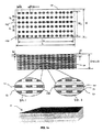
図1aおよび図1bは、多層ホログラフィック導波路データストレージ担体10を示す。それは、ホログラム層11iとクラッド層12iとを各々含む層グループを備えており、ここでiは現在の層インデックスである。ホログラム14ijkは行軸01ijに沿って配置されており、ここでjは現在の行インデックス、kは現在のホログラムインデックスである。行の各々において、ホログラムは重なり合っていない。
Detailed Description Multilayer Holographic Data Storage Carrier FIGS. 1 a and 1 b show a multilayer holographic waveguide
図1aに示す第1の変形では、各グループのホログラム層11iは、同時に、端面結合器15iを有する導波路層である。図1aに示す第2の変形では、グループの各々において、回折格子結合器16i(図1bに示す)を有するホログラム層11iと導波路層13iとは別個に作られ、その間の光学接触で互いに付着されて、ホログラム層への導波の伝導を提供する。双方の変形では、導波路層の外面上に、先行技術のクラッド層と同様の機能を有するクラッド層がある。 In the first variant shown in FIG. 1a, each group of hologram layers 11i is a waveguide layer having an end face coupler 15i at the same time. In the second variant shown in FIG. 1a, in each of the groups, the hologram layer 11i having the grating coupler 16i (shown in FIG. 1b) and the waveguide layer 13i are made separately and attached to each other by optical contact therebetween. To provide guided conduction to the hologram layer. In both variants, there is a cladding layer on the outer surface of the waveguide layer that has the same function as the prior art cladding layer.
図1aおよび図1bでは、h=は行方向におけるホログラムのサイズであり、d=は行方向におけるホログラムのピッチである。h⊥およびd⊥はそれぞれ、横断方向におけるホログラムのサイズおよびピッチである。hはホログラム層の厚さであり、dは層のピッチである。 In FIGS. 1a and 1b, h = is the size of the hologram in the row direction and d = is the pitch of the hologram in the row direction. h⊥ and d⊥ are the size and pitch of the hologram in the transverse direction, respectively. h is the thickness of the hologram layer and d is the layer pitch.
図2aおよび図2bに示すように、読出ビーム20は、結合器15i(または16i)を通って導波路層内へ貫入する。次に、読出ビームは導波21ijとしてそれぞれの行ijに沿って伝搬し、そのホログラムすべてから同時に放射線ビーム22ijkを再構成する。各ホログラムからの再構成された放射線は出力面02に向かって伝搬し、その空間角γが制限される。
As shown in FIGS. 2a and 2b, the
ホログラムが放射線の特定の空間角γを有する場合、隣接するホログラム間のホログラムピッチp=は、平面03に、およびこの平面より上の区域に、前記放射線の交点を提供するよう設定される。再構成された放射線ビームはすべて、平行な平面04に、集束されたデータページ画像を形成する。
If the hologram has a specific spatial angle γ of radiation, the hologram pitch p = between adjacent holograms is set to provide the intersection of the radiation in the
図3は、集束面04におけるデータページ画像パターン51を示す。データ画素17mnはサイズs=、s⊥およびピッチt=、t⊥を有し、2−Dマトリックスとして配置される。mおよびnはそれぞれ、行および列に沿った現在の画素インデックスである。データページ画像はすべて、同じ配向を有する。MおよびNは、それぞれの方向におけるデータ画素の量である。
FIG. 3 shows a data page image pattern 51 on the focusing
図4は、重ね合わされたホログラムを有するホログラム層を示す。平行でない行軸01ijと01′ijとの間の角度はαである。平行でない異なる交差する行に関連するいくつかのホログラムは、少なくとも部分的に重ね合わされるように記録される。2つの最も近接する、平行でないホログラム行同士の間の角度は、前記重ね合わせられたホログラムの角度選択性以上となるように設定される。 FIG. 4 shows a hologram layer with holograms superimposed. The angle between the non-parallel row axes 01ij and 01'ij is α. Several holograms associated with different intersecting rows that are not parallel are recorded to be at least partially overlaid. The angle between the two closest non-parallel hologram rows is set to be equal to or greater than the angle selectivity of the superimposed holograms.
読出方法およびシステム
図5は、多層導波路担体から、ホログラフィックに記録されたデータを検索するためのシステムを示す。このシステムは、多層ホログラフィック導波路データストレージ担体10と、層および行アクセスユニット30とを含む。層および行アクセスユニット30は、干渉性放射線のビームを生成するためのレーザ31と、ビーム24を形成するためのビーム形成器32とで構成されており、ビーム24は、角偏向器33により偏向されてビーム25になり、それは光学素子(レンズ)34を通過して、選択された層11iへ向けられ、それぞれの結合器15i(または16i)を通って、必要なホログラム行に沿って選択された層内を通る。
Readout Method and System FIG. 5 shows a system for retrieving holographically recorded data from a multilayer waveguide carrier. The system includes a multilayer holographic waveguide
「可動窓」の形に作られたホログラムアクセスユニット40は、平面02と平面03(図2a参照)との間の領域に配置されて、任意のホログラム14ijkからの放射線22ijkを分離してそれへのアクセスを獲得し、他の再構成されたホログラムからの放射線を遮断するよう意図されている。
A
多素子光検出器50は、担体の出力面02に向かって面し、前記ホログラムからの再構成された放射線22ijkを受取るよう意図されており、この放射線の集束面04に配置されて、ホログラムにより記憶されたデータの画素パターン51(図3参照)と光学的に結合される。
The
最後に、コンピュータ60は、層および行アクセスユニット61、ホログラムアクセスユニット62および光検出器63の制御入力に、それぞれのインターフェイスユニットを介して接続されて、それらの連係動作を制御する。
Finally, the
図6は、ホログラム層の導波路ホログラム14ijkと光検出器アレイ50との幾何学的関係を示す。
FIG. 6 shows the geometric relationship between the waveguide hologram 14ijk of the hologram layer and the
ホログラム行およびデータ行と平行な一方の方向における光検出器アレイの画素量Q=は以下の式となるはずである。 The pixel quantity Q of the photodetector array in one direction parallel to the hologram row and the data row should be expressed by the following equation.

式中、P=は、行に沿った検出器アレイの線形サイズで、 Where P = is the linear size of the detector array along the row,
となっており、
h=は、1つの行に沿ったホログラムピッチであり、
q=は、その行におけるホログラムの数であり、
p=は、1つの行に沿った検出器画素のピッチであり、
Mは、1つのデータページ行における読出データの画素数である。
And
h = is the hologram pitch along one row,
q = is the number of holograms in the row,
p = is the pitch of the detector pixels along one row,
M is the number of pixels of read data in one data page row.
それぞれ、ホログラム行およびデータページ行に垂直な他方の方向における光検出器アレイ画素量は、以下の式となるはずである。 The photodetector array pixel quantities in the other direction perpendicular to the hologram row and the data page row, respectively, should be:
式中、Q⊥は、列に沿った検出アレイの線形サイズであり、
h⊥は、1つの列に沿ったホログラムピッチであり、
q⊥は、その列におけるホログラムの数であり、
p⊥は、その列に沿った検出器画素のピッチであり、
Nは、1つのデータページ列における読出データの画素数である。
Where Q⊥ is the linear size of the detection array along the column,
h⊥ is the hologram pitch along one row,
q⊥ is the number of holograms in the row,
p⊥ is the pitch of the detector pixels along that column,
N is the number of pixels of read data in one data page column.
![]()
![]()
は、選択された方向におけるホログラム行の線形サイズである。データページ画像の画素のピッチは、検出器画素のピッチと等しいかまたはそれより大きく、その場合、それはその整数の倍数である。 Is the linear size of the hologram row in the selected direction. The pixel pitch of the data page image is equal to or greater than the detector pixel pitch, in which case it is an integer multiple thereof.
図7は、位相共役参照ビーム20*を利用して、多層導波路担体から、ホログラフィックに記憶されたデータを検索するためのシステムを示す。図5と比較して、共役結合器15*iが使用され、光検出器は共役面04*に配置される。
FIG. 7 shows a system for retrieving holographically stored data from a multilayer waveguide carrier using a phase
図8は、重ね合わされた導波路ホログラムの読出のためのシステムである。平行でない行からのホログラムは、角度αをその間に有する読出ビーム20および20′によって読出される。層11iと平行な平面において読出ビーム20の必要なさらなる角度偏位を提供するために、さらなる偏向器が層および行アクセスユニットにおいて使用される。たとえば、偏向器33に加えて回転光学プレート35(コンピュータによりそれぞれのインターフェイスを介して制御されるロータリーアクチュエータが設けられた回転ミラーとして作られる)を使用することが可能である。
FIG. 8 is a system for readout of superimposed waveguide holograms. Holograms from non-parallel rows are read by read
図9は、暗号化された導波路ホログラムの読出のためのシステムである。多チャネル位相空間光変調器41および円柱レンズ36はそれぞれ、読出ビームの符号化(暗号化)、および、符号化されたビーム27ijの導波路層11iへの方向付けのために使用される。
FIG. 9 is a system for reading an encrypted waveguide hologram. The multi-channel phase spatial light modulator 41 and the
図10は、レーザマトリックスによる導波路ホログラムの読出のためのシステムを示す。レーザマトリックス37および光ファイバ38ijは、各ホログラム行について別個の読出ビームを形成するために使用される。コンピュータは、インターフェイス65を介して、マトリックス37の各レーザを制御する。
FIG. 10 shows a system for readout of a waveguide hologram with a laser matrix.
導波路ホログラム記録プロセスおよび装置
ホログラムは、デジタル(バイナリもしくはマルチレベル)信号またはアナログ信号の2次元マトリックスのフーリエ(もしくは擬フーリエ)またはフレネルホログラムとして記録可能である。ホログラムマトリックスは別個の層上に記録される。次に、ホログラム層(および、別個に使用される場合には導波路層も)とクラッド層とはともに挟まれて、それらの間に光学接触を形成し、こうして多層導波路ホログラフィックデータストレージ担体を生成する。
Waveguide Hologram Recording Process and Apparatus Holograms can be recorded as a Fourier (or pseudo-Fourier) or Fresnel hologram of a two-dimensional matrix of digital (binary or multilevel) or analog signals. The hologram matrix is recorded on a separate layer. The hologram layer (and also the waveguide layer if used separately) and the cladding layer are then sandwiched together to form an optical contact between them, thus a multilayer waveguide holographic data storage carrier Is generated.
フーリエ(または擬フーリエ)ホログラム記録
図11は、回折格子結合器を使用することによって光記録層に導波路フーリエ(または擬フーリエ)ホログラムのマトリックスを記録するためのプロセスおよび装置の概略図を表わす。レーザなどの単色性の光源が干渉性放射線のビームを生成し、それは、図11に示すように、第1の(信号)ビーム70と、光学手段32によって参照ビーム28を形成するために使用される第2のビームとに分割される。レンズなどの標準光学手段80によって拡張された信号コリメートビーム71が、空間光変調器(SLM)42を通過する(またはそこから反射する)。データページはSLM42によって表示される。コンピュータ60は制御信号を形成し、信号はインターフェイス66を介してSLM42に到着する。制御信号に従って振幅(または位相、もしくは偏光)が変調されたビーム72が、光学素子(レンズ)81によって、光記録媒体17近傍の平面06に集束され、それに続き、それは光記録媒体17の局所区域を照明する。こうして、この局所区域は、データページのフーリエ(または擬フーリエ)変換関数の画像によって照明される。光記録媒体17の層は、光学的に透明な硬い基材18(たとえばガラス)の上に積層されている。
Fourier (or Pseudo-Fourier) Hologram Recording FIG. 11 represents a schematic diagram of a process and apparatus for recording a matrix of waveguide Fourier (or pseudo-Fourier) holograms on an optical recording layer by using a grating coupler. A monochromatic light source such as a laser generates a beam of coherent radiation, which is used to form a
同時に、参照ビーム28は、回折格子参照ビーム結合器73によって参照導波29に変換される。波29は次に、同じ局所区域を照明する。
At the same time, the
光記録媒体の寄生照明を防止するために、光記録媒体表面の近傍にダイヤフラム83を配置してもよい。 In order to prevent parasitic illumination of the optical recording medium, a diaphragm 83 may be disposed in the vicinity of the optical recording medium surface.
媒体17に記録される変換されたデータページ画像を形成するための光学系は、異なる方法によって実現されてもよく、それらの方法は、以下に記載するような読出ビームの特性に依存する。 The optical system for forming the converted data page image recorded on the medium 17 may be realized by different methods, which depend on the characteristics of the readout beam as described below.
1) 読出ビームが参照ビームの類似物である場合
この場合、(光学素子81が配置されている)平面07と(SLM42が配置されている)平面08との間の距離は、再構成されたデータページ画像が光記録媒体から、ホログラムから読出装置の検出器面までの距離と同じ距離だけ離れて配置されるようになっている。同時に、データページ画素画像のピッチは、光検出器画素のピッチと等しいか、またはその整数の倍数でなければならない。つまり、たとえば、光検出器50(図6)の平面04での読出データ画素画像のピッチが、SLMによって表示される画素のピッチと等しい場合には、平面08と平面07との間の距離Vは、レンズ81の焦点距離の2倍(2F)に等しい。Fは、平面06と平面07との間の距離である。
1) When the readout beam is similar to the reference beam In this case, the distance between the plane 07 (where the
多層ホログラフィック担体10の異なる層11i(図5)は、光検出器面04(図5)から異なる距離Gi(図6)離れて配置されている。したがって、・Fi+Gi=一定と
いう条件を提供することが必要である。この場合、担体すべての層からの再構成されたデータ画像は、同一の尺度を有する。
Different layers 11i (FIG. 5) of the multilayer
光学的に透明な材料の平行プレート82(図11)(または空間位相補償器)が、異なる層から検出器面への光学距離における任意の差を補償するために使用される。このプレートの厚さおよび屈折率は、所与の層11i(図6)と光検出器面04(図6)との間に配置された担体層の光学的類似物を提供するようなものでなければならない。 A parallel plate 82 (FIG. 11) of optically transparent material (or spatial phase compensator) is used to compensate for any differences in optical distance from different layers to the detector surface. The thickness and refractive index of the plate is such that it provides an optical analog of the carrier layer disposed between a given layer 11i (FIG. 6) and the photodetector surface 04 (FIG. 6). There must be.
2) 読出ビーム(図7の20*など)か参照ビームの位相共役である場合
この場合、図12に示すように、SLM42は、平面07のすぐ近くにあるレンズ81からの収束ビーム内にある。
2) When the readout beam (such as 20 * in FIG. 7) or the phase conjugate of the reference beam In this case, as shown in FIG. 12, the
注:この種のホログラムの読出は、ホログラム面01i(図6)と光検出器面04(図6)との間での任意の画像形成光学部品の使用に備えてはいない。 Note: Reading this type of hologram is not in preparation for the use of any imaging optics between hologram surface 01i (FIG. 6) and photodetector surface 04 (FIG. 6).
図13は、図11と同じであるが、より均一なフーリエ画像分布をホログラム記録面05iに提供するランダム位相マスク43を使用する点のみが異なっている概略図を表わす。位相空間光変調器を位相マスク43として使用することが可能である。
FIG. 13 is the same as FIG. 11 but represents a schematic diagram that differs only in that it uses a
ホログラム記録手順
図11に示すように、参照導波29は、導波路内と同様に光記録膜層17内を伝搬する。同時に、変調された信号ビーム(フーリエまたは擬フーリエ画像)が、光記録膜層に直角な線に沿って向けられる。ホログラムは、各記録の後で、記録されるホログラムのピッチサイズh=に等しい特定方向の距離に沿って光記録層を順次移動させることにより、記録される。移動を行なうために2座標位置決め器90が使用され、コンピュータ60によってインターフェイス67を介して制御される。ホログラムのピッチ(図1a、bのh=およびh⊥)は、光検出器画素p=およびp⊥(図6)の整数で割り切れなければならない。記録されたホログラムは、光記録層にマトリックスを形成するホログラム行に配置される。
Hologram Recording Procedure As shown in FIG. 11, the
図13は、2つの異なる層、つまり光記録(感光性)層17と導波路層19とを含む担体を使用した記録手順の変形を示す。特に、参照ビームはプリズム結合器86によって導波路層19内へ向けられる。
FIG. 13 shows a modification of the recording procedure using a carrier comprising two different layers, namely an optical recording (photosensitive)
図12および図14に示すように、参照ビーム28は光記録層17に対し、小さな角度βで向けられる。光記録層が硬い基材を有していない場合、光記録層の屈折率に近い屈折率を有する浸漬層87および88を使用することによって、この層を光学プレート84と85との間に位置付けることが可能である。
As shown in FIGS. 12 and 14, the
フレネルホログラムの記録
この場合、読出は共役参照ビームによって行なわれることになる。記録手順は上述のものと同じであるが、図15に示すように、集束レンズ81およびコリメータレンズ89などの光学素子が、ホログラム記録面05iにSLMデータページ42のフレネル画像を形成する。
Recording of the Fresnel hologram In this case, the reading is performed by a conjugate reference beam. The recording procedure is the same as that described above, but as shown in FIG. 15, optical elements such as a focusing
参照ビームを導波路層に結合するための回折格子の形成
格子結合器16i(図1b)は、ホログラフィック法によって、導波路層でもある光記録層11i(図1a、図1b)の周辺に記録され、または、それは、スタンピング、エッチングもしくは他の公知の方法によって、別個の導波路層13i(図1a、図1b)の周辺に形成される。
Formation of diffraction grating for coupling reference beam to waveguide layer The grating coupler 16i (FIG. 1b) records on the periphery of the optical recording layer 11i (FIGS. 1a, 1b), which is also the waveguide layer, by holographic method. Or it is formed around the separate waveguide layer 13i (FIGS. 1a, 1b) by stamping, etching or other known methods.
重ね合わされたホログラムの記録
記録手順は上述のものと同じであるが、図16に示すように、少なくとも2つの重ね合わされたホログラム91および91′が、参照ビームの異なる伝搬方向29および29′がホログラム記録面05iにある状態で、重複区域に順次記録される。適切な読出ビームによるホログラムの独立した読出を提供するために、参照ビームの方向同士間の最小角度αが必要である。
Recording of superimposed holograms The recording procedure is the same as described above, but as shown in FIG. 16, at least two
暗号化されたホログラムの記録
この記録手順は上述のものと同じであるが、参照ビームは、読出暗号化ビーム27ij(図9)を形成するために使用されたものと同じ方法によって形成される。
Recording the Encrypted Hologram This recording procedure is the same as described above, but the reference beam is formed by the same method as that used to form the read encrypted beam 27ij (FIG. 9).
したがって、例示的な実施例を参照してこの発明を説明してきたが、この説明は限定的な意味で解釈されるよう意図されてはいない。この説明を参照すれば、例示的な実施例のさまざまな変更、およびこの発明の他の実施例が当業者には明らかであろう。したがって、添付された特許請求の範囲がそのような変更または実施例を、この発明の範囲内に該当するものとして網羅することが考えられる。 Thus, while this invention has been described with reference to illustrative embodiments, this description is not intended to be construed in a limiting sense. With reference to this description, various modifications of the illustrative embodiments, and other embodiments of the invention will be apparent to those skilled in the art. Accordingly, it is contemplated that the appended claims will cover such modifications or embodiments as falling within the scope of the invention.
Claims (16)
a) 層の少なくとも2つのグループを含み、各グループは、
i) データを記憶するための複数のホログラム(14ijk)を有するホログラム層(11i)を含み、前記複数のホログラムは1つ以上のホログラム行に配置され、前記行の各々において前記複数のホログラムは重複しておらず、前記行の任意の1つにおける前記複数のホログラムは、1つの導波によって同時に再構成可能であり、前記各グループはさらに、
ii) 結合器(15i)が設けられた導波路層(13i)と、
iii) 隣接する層グループ同士間の前記導波路層の外面上に配置されたクラッド層(12i)とを含み、
各前記ホログラム(14ijk)は、平面の出力面(02)へ向けて放射線を再構成することができ、各前記ホログラムからの前記放射線は、放射線を前記ホログラムの隣接するものから分離することを提供するために、その空間角が制限されており、前記ホログラム層における前記複数のホログラム(14ijk)は、そこからの放射線が共通の集束面(04)に集束されるように記録されており、前記データストレージシステムはさらに、
b) 前記複数のホログラム(14ijk)からの放射線を受取るための光検出器(50)を含み、前記光検出器は、前記共通の集束面(04)に、またはその近傍に配置されており、前記データストレージシステムはさらに、
c) ホログラムアクセスユニット(40)を含み、前記ホログラムアクセスユニットは、前記光検出器(50)または前記ホログラムアクセスユニットの物理的な動きなしで電子的に可動の窓を有し、前記ホログラムアクセスユニットは、前記出力面(02)と前記放射線の交点の平面(03)との間の領域に配置され、前記ホログラムアクセスユニットは、前記複数のホログラムのうちの選択された1つからの放射線を、前記複数のホログラムのうちの他のものからの放射線から分離するよう動作し、前記データストレージシステムはさらに、
d) 呼出ビーム(20)を形成して選択された層へ向け、それぞれの結合器(15i)を通して、前記行のうちの1つに沿ってその中に向けるための層および行アクセスユニット(30)を含む、多層ホログラフィックデータストレージシステム。A multi-layer holographic data storage system,
a) comprising at least two groups of layers, each group
i) includes a hologram layer (11i) having a plurality of holograms (14ijk) for storing data, wherein the plurality of holograms are arranged in one or more hologram rows, wherein the plurality of holograms overlap in each of the rows The plurality of holograms in any one of the rows can be reconstructed simultaneously by a single wave guide, and each group further comprises:
ii) a waveguide layer (13i) provided with a coupler (15i);
iii) a cladding layer (12i) disposed on the outer surface of the waveguide layer between adjacent layer groups,
Each said hologram (14ijk) can reconstruct the radiation towards a flat output surface (02), and said radiation from each said hologram provides to separate the radiation from the adjacent ones of said hologram In order to do so, the spatial angle is limited, and the plurality of holograms (14ijk) in the hologram layer are recorded such that the radiation therefrom is focused on a common focusing surface (04), Data storage systems further
b) including a photodetector (50) for receiving radiation from the plurality of holograms (14ijk), the photodetector being disposed at or near the common focusing surface (04); The data storage system further includes
c) including a hologram access unit (40), the hologram access unit having an electronically movable window without physical movement of the photodetector (50) or the hologram access unit; Is disposed in a region between the output surface (02) and the plane (03) of the intersection of the radiation, and the hologram access unit receives radiation from a selected one of the plurality of holograms, wherein the plurality of operating to separate from the radiation from other ones of the hologram, the data storage system further,
d) A layer and row access unit (30) for directing the calling beam (20) to the selected layer and through each coupler (15i) and into one of the rows therein Multi-layer holographic data storage system.
a) 層の少なくとも2つのグループを含むホログラフィックデータストレージシステムを提供するステップを含み、各グループは、
i) データを記憶するための複数のホログラム(14ijk)を有するホログラム層(11i)を含み、前記複数のホログラムは1つ以上のホログラム行に配置され、前記行の各々において前記複数のホログラムは重複しておらず、前記行の任意の1つにおける前記複数のホログラムは、1つの導波によって同時に再構成可能であり、前記各グループはさらに、
ii) 結合器(15i)が設けられた導波路層(13i)と、
iii) 隣接する層グループ同士間の前記導波路層の外面上に配置されたクラッド層(12i)とを含み、
各前記ホログラム(14ijk)は、平面の出力面(02)へ向けて放射線を再構成することができ、各前記ホログラムからの前記放射線は、放射線を前記複数のホログラムの隣接するものから分離することを提供するために、その空間角が制限されており、前記ホログラム層における前記複数のホログラム(14ijk)は、そこからの放射線が共通の集束面(04)に集束されるように記録されており、前記方法はさらに、
b) 読出ビームを、前記複数のホログラム行の少なくとも1つに沿って、前記導波路層(13i)のうちの選択された1つの中へ、および前記ホログラム層のうちの1つの中へ向け、前記複数のホログラムのうち前記行に配置されたものを再構成するステップと、
c) 読出データを処理するために、選択されたホログラムからの再構成された放射線を、前記共通の集束面で受取るステップとを含み、前記方法は、さらに、
d) 光検出器(50)が、前記複数のホログラム(14ijk)からの放射線を受取るステップを含み、前記光検出器は、前記出力面(02)に向かって面し、かつ前記共通の集束面(04)に、またはその近傍に配置されており、前記方法は、さらに、
e) ホログラムアクセスユニット(40)が、前記複数のホログラムのうちの選択された1つからの放射線を、前記複数のホログラムのうちの他のものからの放射線から分離するステップを含み、前記ホログラムアクセスユニット(40)が、前記光検出器(50)または前記ホログラムアクセスユニットの物理的な動きなしで電子的に可動の窓を有し、前記ホログラムアクセスユニットは、前記出力面(02)と前記放射線の交点の平面(03)との間の領域に配置され、前記方法は、さらに、
f) 層および行アクセスユニット(30)が、呼出ビーム(20)を形成して選択された層へ向け、それぞれの結合器(15i)を通して、前記行のうちの1つに沿ってその中に向けるステップと、
g) コンピュータに含まれるインタフェース(60)が、前記層および行アクセスユニット(30)、前記ホログラムアクセスユニット(40)、および前記光検出器(50)の連係動作を制御し、および読出データを処理するステップを含み、前記インタフェースは、前記層および行アクセスユニット(30)ならびに前記ホログラムアクセスユニット(40)の制御入力と、前記光検出器(50)の制御入力および出力とに接続される、方法。A method for reading data stored in a holographic data storage system (10), comprising:
a) providing a holographic data storage system comprising at least two groups of layers, each group comprising:
i) includes a hologram layer (11i) having a plurality of holograms (14ijk) for storing data, wherein the plurality of holograms are arranged in one or more hologram rows, wherein the plurality of holograms overlap in each of the rows The plurality of holograms in any one of the rows can be reconstructed simultaneously by a single wave guide, and each group further comprises:
ii) a waveguide layer (13i) provided with a coupler (15i);
iii) a cladding layer (12i) disposed on the outer surface of the waveguide layer between adjacent layer groups,
Each hologram (14ijk) can reconstruct radiation towards a planar output surface (02), and the radiation from each hologram separates the radiation from adjacent ones of the plurality of holograms And the plurality of holograms (14ijk) in the hologram layer are recorded such that the radiation from them is focused on a common focusing surface (04). The method further comprises:
b) directing a readout beam along at least one of the plurality of hologram rows into a selected one of the waveguide layers (13i) and into one of the hologram layers; Reconstructing one of the plurality of holograms arranged in the row;
c) receiving reconstructed radiation from selected holograms at the common focusing surface to process readout data , the method further comprising:
d) a photodetector (50) comprising receiving radiation from the plurality of holograms (14ijk), the photodetector facing toward the output surface (02) and the common focusing surface; (04) or in the vicinity thereof, the method further comprises:
e) a hologram access unit (40) comprising separating radiation from a selected one of the plurality of holograms from radiation from the other of the plurality of holograms; A unit (40) has an electronically movable window without physical movement of the photodetector (50) or the hologram access unit, the hologram access unit comprising the output surface (02) and the radiation Arranged in a region between the plane of intersection (03) of
f) A layer and row access unit (30) forms a paging beam (20) towards the selected layer and through each coupler (15i) along one of the rows therein Step to direct,
g) An interface (60) included in the computer controls the coordinated operation of the layer and row access unit (30), the hologram access unit (40), and the photodetector (50) and processes read data The interface is connected to the control input of the layer and row access unit (30) and the hologram access unit (40) and the control input and output of the photodetector (50) .
。15. The method according to claim 14 , wherein the reconstructed radiation is received by a photodetector (50) facing towards the output surface (02) and arranged at the common converging surface (04).
Applications Claiming Priority (3)
| Application Number | Priority Date | Filing Date | Title |
|---|---|---|---|
| CA2,363,279 | 2001-11-16 | ||
| CA2363279A CA2363279C (en) | 2001-11-16 | 2001-11-16 | Waveguide multilayer holographic data storage |
| PCT/CA2002/001849 WO2003044574A1 (en) | 2001-11-16 | 2002-11-18 | Waveguide multilayer holographic data storage |
Publications (2)
| Publication Number | Publication Date |
|---|---|
| JP2005518556A JP2005518556A (en) | 2005-06-23 |
| JP4342311B2 true JP4342311B2 (en) | 2009-10-14 |
Family
ID=4170570
Family Applications (1)
| Application Number | Title | Priority Date | Filing Date |
|---|---|---|---|
| JP2003546148A Expired - Fee Related JP4342311B2 (en) | 2001-11-16 | 2002-11-18 | Waveguide multilayer holographic data storage |
Country Status (9)
| Country | Link |
|---|---|
| US (1) | US7321540B2 (en) |
| EP (1) | EP1449018B1 (en) |
| JP (1) | JP4342311B2 (en) |
| AT (1) | ATE323892T1 (en) |
| AU (1) | AU2002347149A1 (en) |
| CA (1) | CA2363279C (en) |
| DE (1) | DE60210806T2 (en) |
| ES (1) | ES2262866T3 (en) |
| WO (1) | WO2003044574A1 (en) |
Families Citing this family (15)
| Publication number | Priority date | Publication date | Assignee | Title |
|---|---|---|---|---|
| US20050052982A1 (en) * | 2003-09-09 | 2005-03-10 | Lucere, Lp | Virtual head for generating a multi-dimensional data signal |
| JP4339676B2 (en) * | 2003-12-26 | 2009-10-07 | Tdk株式会社 | Access method for multilayer holographic recording medium |
| JP2005352223A (en) * | 2004-06-11 | 2005-12-22 | Sony Corp | Hologram recording and reproducing apparatus with phase conjugate light reproducing system |
| CZ2005413A3 (en) * | 2005-06-24 | 2007-01-31 | Intv, S. R. O. | Optical storage medium and optical device for data recording, deletion and reading |
| JP4769547B2 (en) * | 2005-11-02 | 2011-09-07 | 富士通株式会社 | Hologram recording / reproducing device |
| DE102007004025A1 (en) * | 2007-01-22 | 2008-07-31 | Technische Universität Berlin | Method and device for producing a hologram in an optical medium |
| JP4483898B2 (en) * | 2007-06-08 | 2010-06-16 | ソニー株式会社 | Recording apparatus, reproducing apparatus, recording method, reproducing method, and recording medium |
| CN101329875B (en) * | 2007-06-19 | 2011-06-08 | 建兴电子科技股份有限公司 | Data processing method for holographic optical data storage system |
| KR20080112570A (en) * | 2007-06-21 | 2008-12-26 | 삼성전자주식회사 | Holographic recording/reproducing apparatus |
| EP2012310A1 (en) * | 2007-07-02 | 2009-01-07 | Deutsche Thomson OHG | Holographic storage medium with integrated phase mask |
| JP2009080906A (en) * | 2007-09-26 | 2009-04-16 | Toshiba Corp | Optical information recording/reproducing apparatus, diffraction-grating fabricating apparatus, optical information recording medium, and positioning control method |
| US20110075537A1 (en) * | 2009-09-25 | 2011-03-31 | General Electric Company | Holographic disc with improved features and method for the same |
| JP5286246B2 (en) * | 2009-12-28 | 2013-09-11 | 株式会社日立製作所 | Information processing device |
| KR101955328B1 (en) | 2012-11-14 | 2019-05-30 | 삼성전자주식회사 | Optical head for hologram optical apparatus and method of operating the same |
| GB202104043D0 (en) * | 2021-03-23 | 2021-05-05 | Holomem Ltd | Volumetric Holographic Data Storage Devices and Volumentric Holograms |
Family Cites Families (8)
| Publication number | Priority date | Publication date | Assignee | Title |
|---|---|---|---|---|
| EP0047326B1 (en) | 1980-08-21 | 1984-10-31 | International Business Machines Corporation | Identification card comprising information in holographic form |
| JPS62103681A (en) * | 1985-10-31 | 1987-05-14 | Fujitsu Ltd | Optical card |
| US5295208A (en) * | 1992-02-26 | 1994-03-15 | The University Of Alabama In Huntsville | Multimode waveguide holograms capable of using non-coherent light |
| DE4212717A1 (en) * | 1992-04-16 | 1993-10-21 | Laengerer & Reich Gmbh & Co | Heat exchanger |
| US5940514A (en) * | 1996-04-30 | 1999-08-17 | The Board Of Trustees Of The Leland Stanford Junior University | Encrypted holographic data storage based on orthogonal phase code multiplexing |
| JP3761760B2 (en) | 2000-01-27 | 2006-03-29 | 日本電信電話株式会社 | Data multiplexing hologram memory and data multiplexing hologram memory reproducing apparatus |
| HUP0000532A2 (en) * | 2000-02-07 | 2002-03-28 | Optilink Ab | Method and system for recording information on a holographic card |
| US6909684B2 (en) * | 2001-03-22 | 2005-06-21 | Fuji Xerox Co., Ltd. | Optical recording medium, holographic recording and/or retrieval method and holographic recording and/or retrieval apparatus |
-
2001
- 2001-11-16 CA CA2363279A patent/CA2363279C/en not_active Expired - Fee Related
-
2002
- 2002-11-18 EP EP02782566A patent/EP1449018B1/en not_active Expired - Lifetime
- 2002-11-18 DE DE60210806T patent/DE60210806T2/en not_active Expired - Lifetime
- 2002-11-18 US US10/495,578 patent/US7321540B2/en not_active Expired - Fee Related
- 2002-11-18 JP JP2003546148A patent/JP4342311B2/en not_active Expired - Fee Related
- 2002-11-18 AU AU2002347149A patent/AU2002347149A1/en not_active Abandoned
- 2002-11-18 ES ES02782566T patent/ES2262866T3/en not_active Expired - Lifetime
- 2002-11-18 AT AT02782566T patent/ATE323892T1/en not_active IP Right Cessation
- 2002-11-18 WO PCT/CA2002/001849 patent/WO2003044574A1/en active IP Right Grant
Also Published As
| Publication number | Publication date |
|---|---|
| ES2262866T3 (en) | 2006-12-01 |
| AU2002347149A1 (en) | 2003-06-10 |
| DE60210806D1 (en) | 2006-05-24 |
| CA2363279A1 (en) | 2003-05-16 |
| DE60210806T2 (en) | 2006-11-30 |
| CA2363279C (en) | 2012-11-06 |
| EP1449018A1 (en) | 2004-08-25 |
| WO2003044574A1 (en) | 2003-05-30 |
| US7321540B2 (en) | 2008-01-22 |
| EP1449018B1 (en) | 2006-04-19 |
| ATE323892T1 (en) | 2006-05-15 |
| JP2005518556A (en) | 2005-06-23 |
| US20050201247A1 (en) | 2005-09-15 |
Similar Documents
| Publication | Publication Date | Title |
|---|---|---|
| US6801348B2 (en) | Method and system for recording of information on a holographic medium | |
| EP0836738B1 (en) | Optical storage system | |
| JP4342311B2 (en) | Waveguide multilayer holographic data storage | |
| JP5466833B2 (en) | Method for performing page-based holographic recording and readout | |
| US4104489A (en) | Holographic memory with fringe stabilizing compensation for recording medium motion | |
| KR19990028317A (en) | Multiplexed Hologram Copy System and Method | |
| KR19990028842A (en) | Holographic recording method and hologram retrieval method | |
| US7200097B2 (en) | Parallel recording and reading of diffractive memory using multiple object beams | |
| TW201230023A (en) | Method of parallel bit-wise holographic data storage using a parallel light source | |
| TW479250B (en) | System and method for steering fresnel region data to access data locations in a holographic memory | |
| JP2006154163A (en) | Hologram recording device, hologram reproducing apparatus, hologram recording method, and hologram reproducing method | |
| US5696613A (en) | Method and apparatus for multiplexing data in different planes of incidence of a thin holographic storage media | |
| JP2000242156A (en) | Device and method for recording and reproducing hologram | |
| US6122081A (en) | Using the Talbot Effect for lensless imaging of periodic structures in a holographic memory system | |
| CN100507760C (en) | Quickly duplication diffraction memory for mass production | |
| US20030147327A1 (en) | Holographic storage device with faceted surface structures and associated angle multiplexing method | |
| JPH05181404A (en) | Method and device for hologram recording | |
| Ramenah et al. | Using dichromated gelatin as a diffractive optical storage medium and illustration of multiple applications | |
| Redfield | Holographic storage: not a device, but a storage class | |
| AU701056B2 (en) | Optical storage system | |
| Mehrl et al. | Multiplexed Holographic Data Storage in Bacteriorhodopsin | |
| JPS5953554B2 (en) | One-dimensional hologram writing device |
Legal Events
| Date | Code | Title | Description |
|---|---|---|---|
| A521 | Request for written amendment filed |
Free format text: JAPANESE INTERMEDIATE CODE: A523 Effective date: 20050601 |
|
| A711 | Notification of change in applicant |
Free format text: JAPANESE INTERMEDIATE CODE: A711 Effective date: 20050603 |
|
| A521 | Request for written amendment filed |
Free format text: JAPANESE INTERMEDIATE CODE: A821 Effective date: 20050603 |
|
| A131 | Notification of reasons for refusal |
Free format text: JAPANESE INTERMEDIATE CODE: A131 Effective date: 20080212 |
|
| A601 | Written request for extension of time |
Free format text: JAPANESE INTERMEDIATE CODE: A601 Effective date: 20080509 |
|
| A602 | Written permission of extension of time |
Free format text: JAPANESE INTERMEDIATE CODE: A602 Effective date: 20080526 |
|
| A521 | Request for written amendment filed |
Free format text: JAPANESE INTERMEDIATE CODE: A523 Effective date: 20080611 |
|
| A131 | Notification of reasons for refusal |
Free format text: JAPANESE INTERMEDIATE CODE: A131 Effective date: 20081111 |
|
| A601 | Written request for extension of time |
Free format text: JAPANESE INTERMEDIATE CODE: A601 Effective date: 20090210 |
|
| A602 | Written permission of extension of time |
Free format text: JAPANESE INTERMEDIATE CODE: A602 Effective date: 20090218 |
|
| A521 | Request for written amendment filed |
Free format text: JAPANESE INTERMEDIATE CODE: A523 Effective date: 20090303 |
|
| TRDD | Decision of grant or rejection written | ||
| A01 | Written decision to grant a patent or to grant a registration (utility model) |
Free format text: JAPANESE INTERMEDIATE CODE: A01 Effective date: 20090609 |
|
| A01 | Written decision to grant a patent or to grant a registration (utility model) |
Free format text: JAPANESE INTERMEDIATE CODE: A01 |
|
| A61 | First payment of annual fees (during grant procedure) |
Free format text: JAPANESE INTERMEDIATE CODE: A61 Effective date: 20090707 |
|
| FPAY | Renewal fee payment (event date is renewal date of database) |
Free format text: PAYMENT UNTIL: 20120717 Year of fee payment: 3 |
|
| R150 | Certificate of patent or registration of utility model |
Ref document number: 4342311 Country of ref document: JP Free format text: JAPANESE INTERMEDIATE CODE: R150 Free format text: JAPANESE INTERMEDIATE CODE: R150 |
|
| FPAY | Renewal fee payment (event date is renewal date of database) |
Free format text: PAYMENT UNTIL: 20120717 Year of fee payment: 3 |
|
| FPAY | Renewal fee payment (event date is renewal date of database) |
Free format text: PAYMENT UNTIL: 20130717 Year of fee payment: 4 |
|
| R250 | Receipt of annual fees |
Free format text: JAPANESE INTERMEDIATE CODE: R250 |
|
| R250 | Receipt of annual fees |
Free format text: JAPANESE INTERMEDIATE CODE: R250 |
|
| R250 | Receipt of annual fees |
Free format text: JAPANESE INTERMEDIATE CODE: R250 |
|
| R250 | Receipt of annual fees |
Free format text: JAPANESE INTERMEDIATE CODE: R250 |
|
| R250 | Receipt of annual fees |
Free format text: JAPANESE INTERMEDIATE CODE: R250 |
|
| R250 | Receipt of annual fees |
Free format text: JAPANESE INTERMEDIATE CODE: R250 |
|
| R250 | Receipt of annual fees |
Free format text: JAPANESE INTERMEDIATE CODE: R250 |
|
| LAPS | Cancellation because of no payment of annual fees |