JP4319269B2 - Thin film formation method by plasma CVD - Google Patents
Thin film formation method by plasma CVD Download PDFInfo
- Publication number
- JP4319269B2 JP4319269B2 JP23000798A JP23000798A JP4319269B2 JP 4319269 B2 JP4319269 B2 JP 4319269B2 JP 23000798 A JP23000798 A JP 23000798A JP 23000798 A JP23000798 A JP 23000798A JP 4319269 B2 JP4319269 B2 JP 4319269B2
- Authority
- JP
- Japan
- Prior art keywords
- ticl
- film
- titanium silicide
- titanium
- plasma
- Prior art date
- Legal status (The legal status is an assumption and is not a legal conclusion. Google has not performed a legal analysis and makes no representation as to the accuracy of the status listed.)
- Expired - Fee Related
Links
Images


Description
【0001】
【発明の属する技術分野】
本発明は、半導体装置を製造する工程においてプラズマによる気相成長(CVD)を利用して配線用薄膜を形成する薄膜形成方法およびプラズマCVD装置に関する。
【0002】
【従来の技術】
最近の半導体装置製造の分野において素子の集積化と微細化はますます進んでいる。素子の微細化は製造工程に新しい技術を要求する。ここでは、コンタクトホール底部における配線材料と下地Si(シリコン)との電気的接触を良好し、オーミックコンタクトを得るためのコンタクト形成について説明する。
【0003】
従来のコンタクト形成は、配線材料と下地Siとのバリア膜であるチタン膜をスパッタリング法で形成し、次いでアニールによるコンタクトホール底部のチタンと下地Siとの固相反応を起こし、チタンシリサイドを形成することによって行われていた。このチタンシリサイドが十分に形成されることによって接触抵抗の低い良好なコンタクトが形成された。しかしながら、スパッタリング法を用いる従来のコンタクト形成では、高アスペクト比の微細ホールの底部に十分な厚さのTiを形成することが困難であった。
【0004】
そこで、近年では、段差被覆性の良好なCVD法によるコンタクト形成が提案される。CVD法によるコンタクト形成によればチタン膜やチタンシリサイド膜が成膜される。CVD法によるコンタクト形成の技術では従来2つの例が知られている。第1の例は、チタンのハロゲン化ガス、例えばTiCl4 (四塩化チタン)などを原料とし、コンタクトホール底部に直接TiCl4 と下地Siとを反応させてチタンシリサイド層を形成する技術である(例えば C.Arena,J.Faguet,R.F.Foster,J.T.Hillman,F.Martin and Y.Morand:Advanced Metallization for ULSI Applications in 1994,eds. R Blumenthal and G.Janssen (MRS, Pittsburgh, PA, 1995) p.259 )。第2の例は、チタンのハロゲン化ガス(例えばTiCl4 )とシラン系ガス(Sin H2n+2)とを原料とし、コンタクトホールの内部全体にチタンシリサイド膜を堆積する技術である(例えば、S.Mizuno,M.Tagami,S.Hasegawa and Y.Numasawa:Jpn.J.Appl. Phys.Vol. 36(1997) p.5651 )。以下に、図を参照して、プラズマCVD法によるコンタクト形成技術における上記第1の例と第2の例を詳述する。
【0005】
図5は、上記第1の例を示し、プラズマCVD法によるシリコン基板上の微細コンタクトホール内へのチタン膜およびチタンシリサイド膜の形成工程について模式的に示している。図5で、下方のグラフは、横軸に基板処理の経過時間とそれに対応するステップ(処理工程)をとり、縦軸に膜形成方法で重要となるTiCl4 の流量をとり、各ステップでのTiCl4 の流量制御を示している。上方のコンタクトホールの図は各ステップにおける膜形成状態を示す。図5で、71は基板である下地Si、72は絶縁膜(SiO2 )、73はコンタクトホールである。膜形成は、加熱昇温された基板の直上にH2 (水素)によってプラズマを生成する第1ステップ74と、プラズマ中にTiCl4 を導入して、コンタクトホール73の底部にチタンシリサイド膜76を形成し、さらにコンタクトホール側壁部や上部平坦部にチタン膜77を形成する第2ステップ75によって行われる。
【0006】
シリコン酸化物(SiO2 )であるコンタクトホール側壁部および上部平坦部の表面には、TiCl4 または上記プラズマによってTiCl4 が分解して生成した前駆体(TiClx :以下「TiClx 」と示す)が、プラズマ中で生成された水素ラジカルによって還元される結果、チタン膜が形成される。しかし、コンタクトホール底部ではSiが露出しているため、TiCl4 またはTiClx はSiと反応し、コンタクトホール底部の下地Siの或る厚さ部分がチタンシリサイド層76に置き換わる。この反応の速度は、チタンシリサイド層76中における下地Si71からのSiの拡散またはプラズマ中で生成し表面に吸着したTiClx の拡散によって律速されるので、チタンシリサイド層76の厚さは、温度、TiCl4 の分圧、および時間によって制御される。またこの方法は、コンタクトホール側壁部および上部平坦部に形成されるチタン膜77の堆積速度が、コンタクトホール底部に形成されるチタンシリサイド層76の形成速度よりも非常に遅いため、コンタクトホール側面部および上部平坦部の膜厚に対するコンタクトホール底部の膜厚の比、すなわち底部膜被覆率は非常に良好である。そして、このチタンシリサイド層76が、後の工程でホール内に形成される配線材料と下地Siとの間の拡散バリアとして働き、かつ電気的接触を良好にするという役目を持つ。
【0007】
図6は、上記第2の例を示し、プラズマCVD法によるSi基板上の微細コンタクトホール内へのチタンシリサイド膜の形成について模式的に示している。図6で、下方のグラフは、横軸に基板処理の経過時間とそれに対応するステップをとり、縦軸にTiCl4 とSiH4 の各流量をとって各ステップでのTiCl4 およびSiH4 の流量制御を示す。上方のコンタクトホールの図は、図5と同様に、各ステップにおける膜形成状態を示した図である。膜形成は、加熱昇温された基板の直上にH2 によってプラズマを生成する第1ステップ81と、プラズマ中にTiCl4 およびSiH4 を導入してコンタクトホール73の内外の表面全体にチタンシリサイド膜83を形成する第2ステップ82とから行われる。第2の例では、チタンのハロゲン化ガス(例えばTiCl4 )とシラン系ガス(Sin H2n+2)とを原料としてチタンシリサイド膜83を形成するため、上記プラズマ中に生成するTiClx や塩素ラジカルと下地Siとの反応が非常に抑制されるという利点を有する。
【0008】
【発明が解決しようとする課題】
プラズマCVD法を利用したコンタクト形成における上記第1の例では、反応初期、コンタクトホール底部に露出した下地Si71の表面にチタンシリサイド層76が形成される前に、下地Si表面に、プラズマによってTiCl4 が分解して生成する塩素ラジカルが到達すると、下地Siと激しく反応を起こし、Siが四塩化シリコン(SiCl4 )等として気化し、下地Si層がピット状に急激にエッチングされるという問題がある。図5で77はエッチングされた箇所を指している。このエッチングは反応のごく初期に急激に起こるので、制御することが難しい。その結果、コンタクトホール底部付近にある拡散層を破壊し、電気的不良(主にリーク電流)を発生させる等、素子の信頼性や歩留まりを低下させるという問題を提起する。
【0009】
またプラズマCVD法を利用したコンタクト形成における上記第2の例では、シラン系ガスの反応性が高いため、十分な段差被覆性が得られないという問題が提起される。
【0010】
本発明の目的は、上記問題を解決することにあり、TiCl4 を原料としたプラズマCVDによってチタン膜およびチタンシリサイド膜を形成するにあたり、段差被覆性が良く、かつ下地Si層の浸食を抑制し、信頼性の高い素子を製造する薄膜形成方法およびプラズマCVD装置を提供することにある。
【0011】
【課題を解決するための手段】
本発明に係るプラズマCVDによる薄膜形成方法は、上記目的を達成するために、次のように構成される。
本発明に係るプラズマCVDによる薄膜形成方法(請求項1に対応)は、基板を配置した容器内に四塩化チタン、水素、およびシラン系ガスを導入してプラズマを生成し、基板上にチタンシリサイド膜を形成する方法であり、チタンシリサイド膜を形成する薄膜形成工程は、容器内に水素を導入してプラズマを生成する第1工程と、水素によるプラズマ中にシラン系ガスと四塩化チタンを所定流量まで単位時間当たり一定の割合で増大させて導入し基板上の少なくともコンタクトホール底部にチタンシリサイド膜を形成する第2工程とからなる。
【0012】
【発明の実施の形態】
以下に、本発明の好適な実施形態を添付図面に基づいて説明する。
【0013】
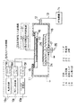
図1と図2を参照して本発明に係るプラズマCVDを利用した薄膜形成方法の第1の実施形態を説明する。図1はコンタクトホールへの薄膜形成方法を模式的に示す。図1で下方のグラフは、横軸に基板処理の経過時間とそれに対応するステップ(処理工程)を示し、縦軸に本発明の膜形成方法で重要となるTiCl4 およびSiH4 の流量をとり、各ステップでのTiCl4 およびSiH4 の流量制御を示している。上方のコンタクトホールの図は各ステップの最後における膜形成状態を示した図である。図2は本薄膜形成方法を実施するプラズマCVD装置の構成を示す。
【0014】
最初に図2を参照してプラズマCVD装置の構成を説明する。処理チャンバを形成する容器11は導電性部材で形成され、アース電位に保持される。容器11の側壁には排気口12が形成され、この排気口12には排気管13を介して排気機構14が接続される。排気機構14によって容器11の内部は所要の減圧状態に保持される。容器11の内部には、天井部に絶縁体15を介して上部電極16が設けられ、底部に絶縁体17を介して基板ホルダ18が設けられる。基板ホルダ18は下部電極として設けられ、上部電極16の下面に平行に設けられている。上部電極16はガス供給部としての機能を有し、反応ガス供給機構19に接続されると共に下面部にガス導入部20が形成されている。反応ガス供給機構19は、H2 供給源19aおよびその供給量を調整するマスフローコントローラ19bと、TiCl4 供給源19cおよびその供給量を調整するマスフローコントローラ19cと、シラン系ガス供給源19eとその供給量を調整するマスフローコントローラ19fとから構成されている。この反応ガス供給機構19によれば、以下の各実施形態による薄膜形成方法で説明されるごとく、マスフローコントローラ19b,19d,19fの各々によって各ガスの供給量を制御することにより、H2 (水素)とTiCl4 (四塩化チタン)とシラン系ガスを工程に応じて選択的に含む反応ガスをガス導入部20に供給することができる。また上部電極16には、高周波電源21と整合回路22からなる高周波電力供給機構23が接続され、処理に必要な電力が供給される。基板ホルダ18の内部には、基板ホルダ18を加熱するためのヒータ24が内蔵され、さらに温度状態を検出するための熱電対25が設けられている。基板ホルダ18の上面には、処理すべき基板26が搭載される。基板26を搬送する機構、基板26を搬入・搬出するポートの図示は省略されている。
【0015】
上記プラズマCVD装置において、容器11の内部は排気口12を通し排気機構14によって減圧状態に維持され、その容器11内の基板ホルダ18上に基板26が載置される。基板ホルダ18はヒータ24と熱電対25によって所定の温度となるように加熱され、基板26の温度は400℃〜650℃の範囲の含まれる一定温度に維持される。基板26はシリコン基板である。図1において31は下地Siであり、基板26に対応する。図1に示すごとく、下地Si31の上には絶縁膜(SiO2 ;シリコン酸化物)32が形成され、絶縁膜32にはコンタクトホール33が形成されている。コンタクトホール33にはチタン膜34およびチタンシリサイド膜35が形成される。チタン膜34およびチタンシリサイド膜35の形成は2つのステップによって構成されている。すなわち膜形成は、加熱昇温された基板の直上にH2 によってプラズマを生成する第1ステップ41と、プラズマ中にTiCl4 を導入して、コンタクトホール33の底部にチタンシリサイド膜35を形成し、さらにコンタクトホール側壁部や上部平坦部にチタン膜34を形成する第2ステップ42によって行われる。
【0016】
第1ステップ41では、反応ガス供給機構19からH2 を100〜1000sccmの範囲内の流量で供給し、ガス導入部20より容器11内にH2 を導入し、容器11内を0.01〜1Torrの範囲内の一定圧力に保った後、高周波電力を高周波電力供給機構23から上部電極16に印加して、容器11内の基板26の直上にプラズマを生成する。本実施形態における印加電力は200〜1000Wであり、印加電力の周波数は13.56〜200MHzである。
【0017】
次に第2ステップ42では、TiCl4 を導入して、コンタクトホール33の底部にチタンシリサイド膜35を形成する。基板26の温度、容器11内の圧力、H2 の流量および高周波電力については第1ステップ41の条件と同じである。TiCl4 の導入は、流量0sccmから所定流量(好ましくは3.5sccm)まで単位時間当たり一定の割合で増大させて導入し、その後一定流量で流してチタンシリサイド膜35を形成する。本実施形態におけるTiCl4 の流量は1〜5sccmであり、0sccmから所定流量まで5秒から15秒の時間をかけて増加させる。図1において第2ステップ42で示された流量特性の前縁の傾斜部43がTiCl4 の上記流量制御の状態を示している。このTiCl4 の流量制御によって、反応初期の塩素ラジカルの量を減少させ、下地Si31のエッチングが抑制された状態でチタンシリサイド膜35が形成される。一旦チタンシリサイド膜35が形成されると、チタンシリサイド膜35の塩素ラジカルに対する化学的耐性が強く下地Si31の保護膜となるため、塩素ラジカルによる下地Si31のエッチングは抑制される。従ってその後は一定流量のTiCl4 が導入される(状態44)。TiCl4 の導入量が一定流量下におけるチタンシリサイド膜35の成長速度は、チタンシリサイド中を、下地Si31からのSiまたはプラズマ中で生成し表面に吸着したTiClx が拡散する速度によって律速される。そのために下地Si31がチタンシリサイド膜35で置換される量を、時間で制御することが可能となる。またコンタクトホール側壁部に形成されるチタン膜34の堆積速度は、チタンシリサイド膜35の成長速度よりも非常に小さいため、底部の膜被覆性が良好となる。
【0018】
上記の第1実施形態による薄膜形成方法によれば、下地Si31のエッチングが抑制され、コンタクトホール底部の膜被覆率が良好なチタン膜34およびチタンシリサイド膜35が形成される。
【0019】
次に図3と前述の図2を参照して本発明に係る薄膜形成方法の第2の実施形態を説明する。第2実施形態による薄膜形成方法が実施される装置構成も図2で示した構成と実質的に同じである。相違する点は反応ガス供給機構19および上部電極16のガス導入部20からTiCl4 に加え、シラン系ガス(Sin H2n+2)、例えばSiH4 が導入される点である。第2実施形態による薄膜形成方法は図3に図解される。図3に示した内容も図1で説明した内容と類似しており、図3で同じ要素には同じ符号を付している。すなわち図3で、31は下地Si、32は絶縁膜、33はコンタクトホール、35はチタンシリサイド膜、34はチタン膜である。相違する点は、下方のグラフにおいて、横軸の経過時間で第1ステップ51、第2ステップ52、第3ステップ53が示され、縦軸の流量で「TiCl4 またはSiH4 」と示されていることである。第2実施形態によるチタン膜およびチタンシリサイド膜の形成は、第1〜第3の3つのステップ51〜53によって行われる。
【0020】
上記第1ステップ51は第1実施形態の第1ステップ41と同じである。すなわち第1ステップ51では、基板ホルダ18上の基板26の温度は400〜650℃の範囲の一定温度に維持され、ガス導入部20からH2 が100〜1000sccm導入され、容器11内を0.01〜1Torrの一定圧力に保ち、高周波電力を高周波電力供給機構23から高周波電力を上部電極16に供給・印加して、容器11内の基板26の直上にプラズマを生成する。印加電力は200〜1000W、周波数は13.56〜200MHzである。
【0021】
上記第2ステップ52では、SiH4 とTiCl4 が導入され、コンタクトホール33の内部および上部平坦部の全体にチタンシリサイド膜35を堆積する。SiH4 およびTiCl4 の導入は、流量0sccmからそれぞれの所定流量(好ましくはSiH4 =1.0sccm、TiCl4 =3.5sccm)まで、単位時間当たり一定の割合で増大させて導入する。本実施形態における条件は、TiCl4 の流量が1〜5sccm、SiH4 の流量が0.2〜1.5sccmであり、0sccmから所定流量までの5秒から15秒の時間をかけて各ガスの流量を増大させる。またTiCl4 とSiH4 の流量比は常に一定値(好ましくは(TiCl4 /SiH4 )=3.5)を保っている。基板26の温度、容器11内の温度、H2 流量および高周波電力は第1ステップ51と同じである。
【0022】
ここで第2ステップ52の効果は、まずプラズマ中で生成する非常に活性なシランラジカルと、同様にプラズマ中で生成するTiClx とが反応して、チタンシリサイド膜35が形成される結果、塩素ラジカルによる下地Si31のエッチングはほぼなくなる。この場合、第1実施形態と同様にTiCl4 の導入における流量制御が、塩素ラジカルの生成量を一層減少させること、さらに、シランラジカルが塩素ラジカルと、プラズマ中か、または表面において反応するため、塩素ラジカルが消費され減少することによって、一層塩素ラジカルによる下地Si31のエッチングは抑制されることになる。また反応初期にシランラジカルとTiClx との反応によってチタンシリサイド膜35を形成するため、TiClx と下地Si31との置換反応も抑制され、下地Si31の表面にチタンシリサイド膜35が堆積する。ここでSiH4 の導入についてもTiCl4 と同じ流量制御が行われ、TiCl4 とSiH4 の流量比は常に一定に保られる。図3において第2ステップ52の流量特性の傾斜部54,55はそれぞれTiCl4 の流量制御の状態とSiH4 の流量制御の状態を示している。
【0023】
次に上記第3ステップ53では、SiH4 の導入を停止し、TiCl4 は第2ステップ54に継続して一定流量で流し、チタン膜34およびチタンシリサイド膜35を堆積する。本実施形態における条件は、TiCl4 流量が1〜5sccmである。基板26の温度、容器11内の温度および高周波電力は第1ステップと同じである。この第3ステップ53では、第2ステップ52で形成されたチタンシリサイド膜35中を、下地Si31からのSiまたはプラズマ中で生成し表面に吸着したTiClx が拡散移動することによって、さらにチタンシリサイド膜35が成長する。第1実施形態と同様に、下地Si31がチタンシリサイド膜35で置換される量を時間で制御することが可能となる。一方、コンタクトホール33の側面および上部平坦部においても第2ステップ52においてチタンシリサイド膜35が形成されているが、第3ステップ53では、このチタンシリサイド膜上にチタン膜34が堆積する。それは、下地がシリコン酸化膜の場合と同じで、Si原子の供給がないからである。このチタン膜34の堆積速度は、コンタクトホール底部におけるチタンシリサイド膜35の成長速度よりも非常に遅いので、やはり第1実施形態と同様にコンタクトホール底部の膜被覆率は良好である。
【0024】
従って第2実施形態の薄膜形成方法によれば、下地Siのエッチングが非常に抑制され、コンタクトホール底部の膜被覆率が良好なチタン膜およびチタンシリサイド膜が形成される。
【0025】
次に図4と前述の図2を参照して本発明に係る薄膜形成方法の第3の実施形態を説明する。第3実施形態による薄膜形成方法が実施される装置構成も図2で示した構成と実質的に同じである。この実施形態でも、反応ガス供給機構19および上部電極16のガス導入部20からTiCl4 とSiH4 が導入される。第3実施形態による薄膜形成方法は図4に図解される。図4に示した内容も図1で説明した内容と類似しており、図4で同じ要素には同じ符号を付している。すなわち図4で、31は下地Si、32は絶縁膜、33はコンタクトホール、35はチタンシリサイド膜、34はチタン膜である。下方のグラフに示すごとく、横軸の経過時間で第1ステップ61、第2ステップ62、第3ステップ63が示され、縦軸の流量で「TiCl4 またはSiH4 」と示される。第3実施形態によるチタン膜およびチタンシリサイド膜の形成は第1〜第3の3つのステップ61〜63によって行われる。
【0026】
第3実施形態による薄膜形成方法における第1ステップ61の内容は前述した第1ステップ41,51とまったく同じである。
【0027】
次の第2ステップ62では、反応ガス供給機構26からSiH4 のガスのみを供給しガス導入部20を通して容器11内に一定時間、一定流量で導入する。本実施形態によるSiH4 の導入流量は5〜100sccm、導入時間は5秒から20秒である。基板26の温度、容器11内の温度、H2 流量および高周波電力は第1ステップ61と同じである。第2ステップ62においては、導入したSiH4 が、プラズマ中で分解されることによって、基板表面に、シリコン原子(Si)層またはシリコン水素化物(SiHx )の吸着層64が形成される。
【0028】
次の第3ステップ63では、反応ガス供給機構19からTiCl4 のガスのみを供給し、ガス導入部20を通して容器11内に一定時間、一定流量で導入する。TiCl4 の導入に際しては、前述した第1と第2の実施形態と同様に、流量0sccmから所定流量まで単位時間当たり一定の割合で増大させて導入する。すなわち本実施形態におけるTiCl4 の流量は1〜5sccmであり、0sccmから所定流量まで5秒から15秒の時間をかけて増加させる。この第3ステップでは、反応初期、プラズマ中で生成するTiClx が、第2ステップ62で形成されたシリコン原子層またはシリコン水素化物の吸着層64と反応し、チタンシリサイド膜35を形成する。このチタンシリサイド膜35の形成において、前述の各実施形態と同様なTiCl4 の導入における流量制御によって塩素ラジカルの生成量が減少し、下地Si31のエッチングが抑制される。その後、TiCl4 の流量一定下で、チタンシリサイド膜35の成長は、上記各実施形態と同様にチタンシリサイド膜31中のSiまたはTiClx の拡散移動によって継続して起こる。上記各実施形態と同様に、下地Si31がチタンシリサイド膜35で置換される量を時間で制御することが可能となる。またコンタクトホール33の側面、上部平坦部においてもプラズマ中で生成したTiClx が、第2ステップ62で形成されたシリコン原子層またはシリコン水素化物の吸着層64と反応し、チタンシリサイド膜35を形成するが、シリコン原子層またはシリコン水素化物が消費された後はチタン膜34が形成される。ここで、第2ステップ62で形成されたシリコン原子層またはシリコン水素化物の吸着層64は段差被覆性が良好であるため、第3ステップ63で形成されるチタンシリサイド膜35は、第2実施形態で形成されるSiH4 とTiCl4 の反応で形成されるチタンシリサイド膜よりも、より段差被覆率が良好である。さらに上部平坦部に形成されるチタン膜の堆積速度は、コンタクトホール底部におけるチタンシリサイド膜の成長速度よりも非常に遅いので、やはり底部の膜被覆率が良好である。
【0029】
従って第3実施形態の薄膜形成方法によれば、塩素ラジカルによる下地Siのエッチングが抑制され、コンタクトホールにおける側壁部の段差被覆率および底部の膜被覆率が良好なチタン膜およびチタンシリサイド膜が形成される。
【0030】
上記の実施形態では、本発明に係る薄膜形成方法を平行平板型プラズマCVD装置に適用した例を説明したが、本発明を他の形式のプラズマCVD装置、例えばECR型プラズマCVD装置、誘導結合型プラズマCVD装置などを用いることも可能である。
【0031】
【発明の効果】
以上の説明で明らかなように本発明によれば、プラズマCVDを利用して基板の表面に配線用薄膜を形成する薄膜形成方法において、プラズマの中に導入する反応ガスの初期の導入量あるいは導入の仕方を所定方法で制御するようにしたため、下地Siのエッチングが抑制され、さらに段差被覆性やコンタクトホール底部への膜被覆性に優れたチタン膜およびチタンシリサイド膜の成膜を行うことができる。
【図面の簡単な説明】
【図1】本発明に係る薄膜形成方法の第1実施形態を示す説明図である。
【図2】本発明に係る薄膜形成方法が実施されるプラズマCVD装置の内部構造を示した縦断面図である。
【図3】本発明に係る薄膜形成方法の第2実施形態を示す説明図である。
【図4】本発明に係る薄膜形成方法の第3実施形態を示す説明図である。
【図5】従来の薄膜形成方法の第1の例を説明する図である。
【図6】従来の薄膜形成方法の第2の例を説明する図である。
【符号の説明】
11 容器
16 上部電極
18 基板ホルダ
20 ガス導入部
26 基板
31 下地Si(シリコン)
32 絶縁膜(SiO2 )
33 コンタクトホール
34 チタン膜
35 チタンシリサイド膜
64 Si吸着層[0001]
BACKGROUND OF THE INVENTION
The present invention relates to a thin film forming method and a plasma CVD apparatus for forming a thin film for wiring using vapor phase growth (CVD) by plasma in a process of manufacturing a semiconductor device.
[0002]
[Prior art]
In the recent field of semiconductor device manufacturing, the integration and miniaturization of elements are increasingly advanced. Miniaturization of elements requires new technology in the manufacturing process. Here, a description will be given of contact formation for improving the electrical contact between the wiring material and the underlying Si (silicon) at the bottom of the contact hole and obtaining an ohmic contact.
[0003]
In conventional contact formation, a titanium film that is a barrier film between a wiring material and underlying Si is formed by sputtering, and then a solid phase reaction between titanium at the bottom of the contact hole and underlying Si is caused by annealing to form titanium silicide. It was done by that. Good contact with low contact resistance was formed by sufficiently forming this titanium silicide. However, in the conventional contact formation using the sputtering method, it is difficult to form Ti having a sufficient thickness at the bottom of a high aspect ratio fine hole.
[0004]
Therefore, in recent years, contact formation by a CVD method with good step coverage is proposed. According to the contact formation by the CVD method, a titanium film or a titanium silicide film is formed. Conventionally, two examples of the contact forming technique by the CVD method are known. The first example is a technique for forming a titanium silicide layer by reacting TiCl 4 and underlying Si directly at the bottom of a contact hole using a titanium halide gas such as TiCl 4 (titanium tetrachloride) as a raw material ( For example, C.Arena, J.Faguet, RFFoster, JTHillman, F.Martin and Y.Morand: Advanced Metallization for ULSI Applications in 1994, eds.R Blumenthal and G.Janssen (MRS, Pittsburgh, PA, 1995) p.259) . A second example is a technique in which a titanium silicide film is deposited on the entire inside of a contact hole using a titanium halide gas (for example, TiCl 4 ) and a silane-based gas (Si n H 2n + 2 ) as raw materials (for example, S. Mizuno, M. Tagami, S. Hasegawa and Y. Numasawa: Jpn. J. Appl. Phys. Vol. 36 (1997) p. 5651). The first example and the second example in the contact formation technique by the plasma CVD method will be described below in detail with reference to the drawings.
[0005]
FIG. 5 shows the first example and schematically shows a process of forming a titanium film and a titanium silicide film in a fine contact hole on a silicon substrate by plasma CVD. In the lower graph of FIG. 5, the horizontal axis indicates the elapsed time of the substrate processing and the corresponding steps (processing steps), and the vertical axis indicates the flow rate of TiCl 4 that is important in the film forming method. The flow control of TiCl 4 is shown. The upper contact hole shows the film formation state in each step. In FIG. 5,
[0006]
TiCl 4 or a precursor formed by decomposition of TiCl 4 by the above plasma (TiCl x : hereinafter referred to as “TiCl x ”) is formed on the surface of the contact hole sidewall portion and the upper flat portion made of silicon oxide (SiO 2 ). As a result of being reduced by hydrogen radicals generated in the plasma, a titanium film is formed. However, since Si is exposed at the bottom of the contact hole, TiCl 4 or TiCl x reacts with Si, and a certain thickness portion of the underlying Si at the bottom of the contact hole is replaced with the
[0007]
FIG. 6 shows the second example and schematically shows the formation of a titanium silicide film in a fine contact hole on the Si substrate by the plasma CVD method. In Figure 6, the lower graph shows, taking the elapsed time and steps corresponding to those of the substrate processing in the horizontal axis, the vertical axis is the flow rate of TiCl 4 and SiH 4 flow rate of TiCl 4 and SiH 4 at each step Indicates control. The upper contact hole is a diagram showing the state of film formation in each step, as in FIG. In the film formation, a
[0008]
[Problems to be solved by the invention]
In the first example of contact formation using the plasma CVD method, TiCl 4 is formed on the surface of the underlying Si by plasma before the
[0009]
In the second example of contact formation using the plasma CVD method, there is a problem that sufficient step coverage cannot be obtained because of the high reactivity of the silane-based gas.
[0010]
An object of the present invention is to solve the above-described problem. In forming a titanium film and a titanium silicide film by plasma CVD using TiCl 4 as a raw material, the step coverage is good and erosion of the underlying Si layer is suppressed. Another object of the present invention is to provide a thin film forming method and a plasma CVD apparatus for manufacturing a highly reliable element.
[0011]
[Means for Solving the Problems]
In order to achieve the above object, a thin film formation method by plasma CVD according to the present invention is configured as follows .
In the thin film formation method by plasma CVD according to the present invention (corresponding to claim 1 ), titanium tetrachloride, hydrogen, and a silane-based gas are introduced into a container in which a substrate is placed to generate plasma, and titanium silicide is formed on the substrate. A thin film forming process for forming a titanium silicide film is a method for forming a film. The first process is to generate hydrogen by introducing hydrogen into a container, and a silane-based gas and titanium tetrachloride are predetermined in the hydrogen plasma. This is a second step in which a flow rate is increased at a constant rate per unit time and introduced to form a titanium silicide film at least at the bottom of the contact hole on the substrate.
[0012]
DETAILED DESCRIPTION OF THE INVENTION
Preferred embodiments of the present invention will be described below with reference to the accompanying drawings.
[0013]
A first embodiment of a thin film forming method using plasma CVD according to the present invention will be described with reference to FIGS. FIG. 1 schematically shows a method for forming a thin film in a contact hole. In the lower graph of FIG. 1, the horizontal axis indicates the elapsed time of the substrate processing and the corresponding steps (processing steps), and the vertical axis indicates the flow rates of TiCl 4 and SiH 4 that are important in the film forming method of the present invention. The flow control of TiCl 4 and SiH 4 at each step is shown. The upper contact hole is a diagram showing the film formation state at the end of each step. FIG. 2 shows the configuration of a plasma CVD apparatus for carrying out this thin film forming method.
[0014]
First, the configuration of the plasma CVD apparatus will be described with reference to FIG. The
[0015]
In the plasma CVD apparatus, the inside of the
[0016]
In the
[0017]
Next, in a
[0018]
According to the thin film forming method according to the first embodiment, the etching of the
[0019]
Next, a second embodiment of the thin film forming method according to the present invention will be described with reference to FIG. 3 and FIG. The apparatus configuration in which the thin film forming method according to the second embodiment is carried out is substantially the same as the configuration shown in FIG. The difference is that a silane-based gas (Si n H 2n + 2 ), eg, SiH 4, is introduced in addition to TiCl 4 from the reaction
[0020]
The
[0021]
In the
[0022]
Here, the effect of the
[0023]
Next, in the
[0024]
Therefore, according to the thin film forming method of the second embodiment, etching of the underlying Si is greatly suppressed, and a titanium film and a titanium silicide film having a good film coverage at the bottom of the contact hole are formed.
[0025]
Next, a third embodiment of the thin film forming method according to the present invention will be described with reference to FIG. 4 and FIG. The apparatus configuration in which the thin film forming method according to the third embodiment is carried out is substantially the same as the configuration shown in FIG. Also in this embodiment, TiCl 4 and SiH 4 are introduced from the reaction
[0026]
The contents of the
[0027]
In the next
[0028]
In the next
[0029]
Therefore, according to the thin film formation method of the third embodiment, etching of the underlying Si by chlorine radicals is suppressed, and a titanium film and a titanium silicide film are formed that have good step coverage at the side wall and film coverage at the bottom in the contact hole. Is done.
[0030]
In the above embodiment, an example in which the thin film forming method according to the present invention is applied to a parallel plate type plasma CVD apparatus has been described. However, the present invention may be applied to other types of plasma CVD apparatuses such as an ECR type plasma CVD apparatus and an inductively coupled type. It is also possible to use a plasma CVD apparatus or the like.
[0031]
【The invention's effect】
As is apparent from the above description, according to the present invention, in the thin film forming method for forming a thin film for wiring on the surface of a substrate using plasma CVD, the initial introduction amount or introduction of the reactive gas introduced into the plasma. Since the etching method is controlled by a predetermined method, etching of the underlying Si is suppressed, and a titanium film and a titanium silicide film having excellent step coverage and excellent film coverage on the bottom of the contact hole can be formed. .
[Brief description of the drawings]
FIG. 1 is an explanatory view showing a first embodiment of a thin film forming method according to the present invention.
FIG. 2 is a longitudinal sectional view showing an internal structure of a plasma CVD apparatus in which a thin film forming method according to the present invention is implemented.
FIG. 3 is an explanatory view showing a second embodiment of the thin film forming method according to the present invention.
FIG. 4 is an explanatory view showing a third embodiment of a thin film forming method according to the present invention.
FIG. 5 is a diagram illustrating a first example of a conventional thin film forming method.
FIG. 6 is a diagram illustrating a second example of a conventional thin film forming method.
[Explanation of symbols]
11
32 Insulating film (SiO 2 )
33
Claims (1)
前記チタンシリサイド膜を形成する薄膜形成工程は、前記容器内に水素を導入してプラズマを生成する第1工程と、水素によるプラズマ中にシラン系ガスと四塩化チタンを所定流量まで単位時間当たり一定の割合で増大させて導入し基板上の少なくともコンタクトホール底部にチタンシリサイド膜を形成する第2工程とからなることを特徴とするプラズマCVDによる薄膜形成方法。In a thin film formation method by plasma CVD in which titanium tetrachloride, hydrogen, and a silane-based gas are introduced into a container in which a substrate is arranged to generate plasma, and a titanium silicide film is formed on the substrate.
The thin film forming step for forming the titanium silicide film includes a first step of introducing plasma into the vessel to generate plasma, and a constant amount of silane-based gas and titanium tetrachloride in the plasma by hydrogen up to a predetermined flow rate per unit time. And a second step of forming a titanium silicide film at least at the bottom of the contact hole on the substrate by introducing at an increased rate.
Priority Applications (1)
| Application Number | Priority Date | Filing Date | Title |
|---|---|---|---|
| JP23000798A JP4319269B2 (en) | 1998-07-31 | 1998-07-31 | Thin film formation method by plasma CVD |
Applications Claiming Priority (1)
| Application Number | Priority Date | Filing Date | Title |
|---|---|---|---|
| JP23000798A JP4319269B2 (en) | 1998-07-31 | 1998-07-31 | Thin film formation method by plasma CVD |
Publications (3)
| Publication Number | Publication Date |
|---|---|
| JP2000058484A JP2000058484A (en) | 2000-02-25 |
| JP2000058484A5 JP2000058484A5 (en) | 2005-10-27 |
| JP4319269B2 true JP4319269B2 (en) | 2009-08-26 |
Family
ID=16901145
Family Applications (1)
| Application Number | Title | Priority Date | Filing Date |
|---|---|---|---|
| JP23000798A Expired - Fee Related JP4319269B2 (en) | 1998-07-31 | 1998-07-31 | Thin film formation method by plasma CVD |
Country Status (1)
| Country | Link |
|---|---|
| JP (1) | JP4319269B2 (en) |
Cited By (1)
| Publication number | Priority date | Publication date | Assignee | Title |
|---|---|---|---|---|
| WO2021089424A1 (en) * | 2019-11-05 | 2021-05-14 | Aixtron Se | Use of a cvd reactor for depositing two-dimensional layers |
Families Citing this family (7)
| Publication number | Priority date | Publication date | Assignee | Title |
|---|---|---|---|---|
| KR100762863B1 (en) * | 2000-06-30 | 2007-10-08 | 주식회사 하이닉스반도체 | METHOD OF FABRICATING COPPER-LINE UTILIZED Ti-Si-N FILM FOR PREVENTING DIFFUSION |
| JP2002203810A (en) * | 2000-12-28 | 2002-07-19 | Tokyo Electron Ltd | Method for manufacturing semiconductor device, semiconductor device, and apparatus for manufacturing semiconductor device |
| JP2002363759A (en) * | 2001-06-12 | 2002-12-18 | Tokyo Electron Ltd | Plasma treatment device, plasma treatment method, and method for detecting timing of charging trace amount of gas |
| US7968463B2 (en) | 2006-05-25 | 2011-06-28 | Renesas Electronics Corporation | Formation method of metallic compound layer, manufacturing method of semiconductor device, and formation apparatus for metallic compound layer |
| JP5193494B2 (en) * | 2007-04-27 | 2013-05-08 | 東京エレクトロン株式会社 | Ti film forming method and storage medium |
| JP6426893B2 (en) * | 2013-12-25 | 2018-11-21 | 東京エレクトロン株式会社 | Method of forming contact layer |
| KR101872813B1 (en) | 2016-12-26 | 2018-06-29 | 주식회사 인코어드 테크놀로지스 | Method and apparatus for determining abnormal events related to in-home person |
-
1998
- 1998-07-31 JP JP23000798A patent/JP4319269B2/en not_active Expired - Fee Related
Cited By (2)
| Publication number | Priority date | Publication date | Assignee | Title |
|---|---|---|---|---|
| WO2021089424A1 (en) * | 2019-11-05 | 2021-05-14 | Aixtron Se | Use of a cvd reactor for depositing two-dimensional layers |
| CN114901865A (en) * | 2019-11-05 | 2022-08-12 | 艾克斯特朗欧洲公司 | Use of a CVD reactor for depositing two-dimensional layers |
Also Published As
| Publication number | Publication date |
|---|---|
| JP2000058484A (en) | 2000-02-25 |
Similar Documents
| Publication | Publication Date | Title |
|---|---|---|
| US5326404A (en) | Plasma processing apparatus | |
| JP5294694B2 (en) | In situ deposition of silicon and titanium nitride | |
| US5946594A (en) | Chemical vapor deposition of titanium from titanium tetrachloride and hydrocarbon reactants | |
| JP4919535B2 (en) | Plasma treatment of thermal CVD TaN films from tantalum halide precursors | |
| US6218301B1 (en) | Deposition of tungsten films from W(CO)6 | |
| US7484513B2 (en) | Method of forming titanium film by CVD | |
| US5508066A (en) | Method for forming a thin film | |
| US20050221000A1 (en) | Method of forming a metal layer | |
| JPH10144628A (en) | Improved deposition method of thin film | |
| WO2002079537A2 (en) | W-cvd with fluorine-free tungsten nucleation | |
| WO2004059707A2 (en) | A method and apparatus for forming a high quality low temperature silicon nitride film | |
| US20090071404A1 (en) | Method of forming titanium film by CVD | |
| KR100247515B1 (en) | A method of depositing thin film by plasma-enhanced chemical vapor deposition | |
| KR101217980B1 (en) | Method for depositing tungsten layers using sequential flow deposition | |
| JP4319269B2 (en) | Thin film formation method by plasma CVD | |
| JP2022516870A (en) | Methods and equipment for enhancing the selectivity of titanium and titanium silicate during chemical vapor deposition | |
| US6168837B1 (en) | Chemical vapor depositions process for depositing titanium silicide films from an organometallic compound | |
| WO2022080153A1 (en) | Substrate processing method and substrate processing apparatus | |
| Sim et al. | Method to enhance atomic-layer deposition of tungsten–nitride diffusion barrier for Cu interconnect | |
| JPH0613332A (en) | Plasma cvd method and manufacture of semiconductor device | |
| JPH1064849A (en) | Method and apparatus for manufacturing thin film | |
| JP4312291B2 (en) | Film formation method by plasma CVD | |
| JP3534676B2 (en) | Method and apparatus for forming Cu or Cu-containing film | |
| US20230377892A1 (en) | Methods and apparatus for processing a substrate | |
| JPH09306870A (en) | Forming barrier film |
Legal Events
| Date | Code | Title | Description |
|---|---|---|---|
| A521 | Written amendment |
Free format text: JAPANESE INTERMEDIATE CODE: A523 Effective date: 20050729 |
|
| A621 | Written request for application examination |
Free format text: JAPANESE INTERMEDIATE CODE: A621 Effective date: 20050729 |
|
| A977 | Report on retrieval |
Free format text: JAPANESE INTERMEDIATE CODE: A971007 Effective date: 20061004 |
|
| A131 | Notification of reasons for refusal |
Free format text: JAPANESE INTERMEDIATE CODE: A131 Effective date: 20090224 |
|
| A521 | Written amendment |
Free format text: JAPANESE INTERMEDIATE CODE: A523 Effective date: 20090422 |
|
| TRDD | Decision of grant or rejection written | ||
| A01 | Written decision to grant a patent or to grant a registration (utility model) |
Free format text: JAPANESE INTERMEDIATE CODE: A01 Effective date: 20090526 |
|
| A01 | Written decision to grant a patent or to grant a registration (utility model) |
Free format text: JAPANESE INTERMEDIATE CODE: A01 |
|
| A61 | First payment of annual fees (during grant procedure) |
Free format text: JAPANESE INTERMEDIATE CODE: A61 Effective date: 20090528 |
|
| FPAY | Renewal fee payment (event date is renewal date of database) |
Free format text: PAYMENT UNTIL: 20120605 Year of fee payment: 3 |
|
| R150 | Certificate of patent or registration of utility model |
Free format text: JAPANESE INTERMEDIATE CODE: R150 |
|
| FPAY | Renewal fee payment (event date is renewal date of database) |
Free format text: PAYMENT UNTIL: 20130605 Year of fee payment: 4 |
|
| R250 | Receipt of annual fees |
Free format text: JAPANESE INTERMEDIATE CODE: R250 |
|
| R250 | Receipt of annual fees |
Free format text: JAPANESE INTERMEDIATE CODE: R250 |
|
| R250 | Receipt of annual fees |
Free format text: JAPANESE INTERMEDIATE CODE: R250 |
|
| R250 | Receipt of annual fees |
Free format text: JAPANESE INTERMEDIATE CODE: R250 |
|
| R250 | Receipt of annual fees |
Free format text: JAPANESE INTERMEDIATE CODE: R250 |
|
| LAPS | Cancellation because of no payment of annual fees |