JP4305802B2 - Light-emitting diode lighting circuit - Google Patents
Light-emitting diode lighting circuit Download PDFInfo
- Publication number
- JP4305802B2 JP4305802B2 JP2001037001A JP2001037001A JP4305802B2 JP 4305802 B2 JP4305802 B2 JP 4305802B2 JP 2001037001 A JP2001037001 A JP 2001037001A JP 2001037001 A JP2001037001 A JP 2001037001A JP 4305802 B2 JP4305802 B2 JP 4305802B2
- Authority
- JP
- Japan
- Prior art keywords
- light emitting
- emitting diode
- lighting circuit
- voltage
- light
- Prior art date
- Legal status (The legal status is an assumption and is not a legal conclusion. Google has not performed a legal analysis and makes no representation as to the accuracy of the status listed.)
- Expired - Lifetime
Links
- 239000004065 semiconductor Substances 0.000 claims description 36
- 239000004973 liquid crystal related substance Substances 0.000 claims description 15
- 238000001514 detection method Methods 0.000 claims description 7
- 239000003086 colorant Substances 0.000 claims description 3
- 239000003990 capacitor Substances 0.000 description 17
- QSHDDOUJBYECFT-UHFFFAOYSA-N mercury Chemical compound [Hg] QSHDDOUJBYECFT-UHFFFAOYSA-N 0.000 description 4
- 229910052753 mercury Inorganic materials 0.000 description 4
- 238000004804 winding Methods 0.000 description 3
- 230000007613 environmental effect Effects 0.000 description 2
- 238000009499 grossing Methods 0.000 description 2
- 238000010586 diagram Methods 0.000 description 1
- 230000000694 effects Effects 0.000 description 1
- 238000000034 method Methods 0.000 description 1
- 230000010355 oscillation Effects 0.000 description 1
- 230000010349 pulsation Effects 0.000 description 1
- 229910052724 xenon Inorganic materials 0.000 description 1
- FHNFHKCVQCLJFQ-UHFFFAOYSA-N xenon atom Chemical compound [Xe] FHNFHKCVQCLJFQ-UHFFFAOYSA-N 0.000 description 1
Images


Landscapes
- Circuit Arrangement For Electric Light Sources In General (AREA)
- Control Of Indicators Other Than Cathode Ray Tubes (AREA)
- Led Devices (AREA)
- Liquid Crystal (AREA)
- Non-Portable Lighting Devices Or Systems Thereof (AREA)
Description
【0001】
【発明の属する技術分野】
本発明は、発光ダイオード群を発光させる点灯回路であって、特にはノートパソコンや液晶テレビなどの、ディスプレイに使用される液晶バックライト駆動回路に関するものである。
【0002】
【従来の技術】
従来の液晶バックライト駆動回路は、直流電圧を数十kHzの交流電圧に変換した後、トランスによって数百Vに昇圧した後、冷陰極蛍光管に印加して発光させる方式であった。
【0003】
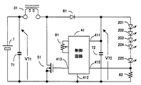
図4は、従来の冷陰極蛍光管の液晶バックライト駆動回路構成であり、図5はその主要部における電圧波形である。図4において、DC/DCコンバータは半導体スイッチ53,インダクタ32、コンデンサ73およびダイオード63で構成され、制御回路42の可変抵抗81の設定値によりコンデンサ73の両端から任意の可変直流電圧を得るものである。ここで、端子421は制御回路42の電源端子であり、端子422は制御回路42のグランドの共通端子であり、端子423は半導体スイッチ53の駆動端子であり、端子424は冷陰極蛍光管2の電流検出端子である。直流電源1の電圧V71は半導体スイッチ53の開および閉動作時間に応じたパルス状電圧V63に変換され、平滑回路によって直流電圧V73となる。この直流電圧V73は半導体スイッチ53の閉動作時間(TON)と開動作時間(TOFF)の比率により任意に選ぶことができる。従って、可変直流電圧はV73=V71×TON/(TON+TOFF)で計算される。
【0004】
次に、電圧制御された直流電圧V73はインダクタ33を介してトランス34の中間タップ342に印加される。端子341には半導体スイッチ54が、また端子343には半導体スイッチ55が接続されると共に、コンデンサ74が並列に接続されている。共振回路はトランス34の1次側から見たインダクタンスとコンデンサ74とで構成される。半導体スイッチ54および55は、端子346、347の駆動巻線の働きにより、前記共振回路の周波数のタイミングの開、閉動作を行う。トランス34の2次側端子344と345間に正弦波電圧V72を得ることができる。冷陰極蛍光管2の電流を抵抗85で検出して、制御回路42により、コンデンサ73の電圧V73を制御することで、冷陰極蛍光管2の電流を安定化している。
【0005】
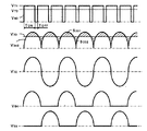
この自励共振型発振回路は、トランス34の端子341と343間のインダクタンスとコンデンサ74で決まる共振周波数で共振し、正弦波電圧V72がトランス34の端子間341−343、344−345あるいは346−347から得られる。図5に示すV54の電圧波形は半導体スイッチ54のコレクターエミッタ間電圧である。ベースに接続されている端子347が負電圧のときは半導体スイッチ54が開動作期間となっているため、半導体スイッチ54のコレクタに接続している端子341の電圧は正弦波電圧が印加されるが、端子347が正電圧に変わると閉動作期間となり、端子341の電圧は差がなくなる。一方、半導体スイッチ55の電圧波形はV55に示すように、V54と逆位相関係である。
トランス34の巻線電圧波形は、V54とV55の合成電圧になり、その電圧波形は、図5のV72の通り、正弦波の高電圧波形である。
【0006】
V342はトランス34の端子342の電圧波形である。コンデンサ73の直流電圧V73と端子342の電圧V342の差電圧が、インダクタ33の端子間に現れることになる。インダクタ33の端子間には、電圧時間積S331とS332に等しい電圧脈動分を含む。このため、トランス34の端子342の平均電圧値とコンデンサ73の電圧値が等しい。
冷陰極蛍光管2に電流を流すために、電圧V72はトランス34で、約1000Vの実効電圧が必要である。
【0007】
【発明が解決しようとする課題】
近年地球環境問題より、水銀を使用の冷陰極蛍光管は代替光源を求められている。水銀を使用しない光源はあるもののキセノン管は、高電圧パルス電圧で点灯させるために、インバータ回路が大型で、ノートパソコンや液晶テレビなどには使用が困難とされている。
そこで、発光ダイオードを代替光源として検討されている。しかし、従来の冷陰極蛍光管の入力電力は、3W(600V×5mA)程度であるのに対して、発光ダイオードは、1個あたりに入力できる電力が40mW(2V×20mA)程度であるため、携帯電話など小型の液晶ディスプレイには使用されるものの、ノートパソコンなどの大型液晶ディスプレイには、発光力の不足で使用できないとされていた。同じ電力を入力するためには、75個(3W/0.04W)の発光ダイオードが必要になり、その駆動回路の数も増えて小型にできなかった。
1つの駆動回路で発光ダイオードを並列接続すると、発光ダイオードの順電圧バラツキが大きく、電流値が大きくバラツキ発光できないものが発生するため、発光ダイオードの数と同じ駆動回路の数が必要とされていた。
【0008】
【課題を解決するための手段】
本発明は、複数の発光ダイオードを直列接続した発光ダイオード群を発光させる点灯回路であって、昇圧型DC/DCコンバータ回路と、その入力端子に接続される直流電源と、前記直流電源と接続されたインダクタ又は単巻トランスと、前記インダクタ又は単巻トランスとグランド間に接続された半導体スイッチと、前記昇圧型DC/DCコンバータ回路の出力端子に接続される発光ダイオード群と、前記発光ダイオード群と接続される電流検出用抵抗を備え、前記昇圧型DC/DCコンバータ回路は、前記電流検出用抵抗の端子間電圧を検出し、制御回路の基準電圧と比較して得られた誤差電圧をパルス幅信号に変換し、前記パルス幅信号に基づいて半導体スイッチを開閉駆動して昇圧動作させて発光ダイオードを定電流制御するとともに、前記基準電圧を変化させることで、前記発光ダイオードの電流値を変化させて調光し、半導体スイッチを開状態として昇圧動作を停止して発光ダイオードを消灯することを特徴とする発光ダイオード点灯回路である。
本発明においては、発光ダイオード群の負電位側に半導体スイッチを接続して発光ダイオードが消灯された場合のもれ電流を防ぐのも好ましい。
また前記発光ダイオードは白色発光ダイオードや赤色、青色、緑色発光ダイオードを使用することが出来る。
それぞれ発光色が異なる発光ダイオードを接続した発光ダイオード点灯回路を3回路以上構成し、各発光ダイオード点灯回路による発光ダイオードの輝度をそれぞれ調整して、発光色を白色や他の色とすることも可能である。
発光ダイオード点灯回路を液晶バックライトに用いるのも好ましく、前記発光ダイオードの発光色を赤色、青色、緑色の3種類とし、各発光ダイオードの輝度をそれぞれ調整して液晶ディスプレイの色補正を行うことも出来る。
【0009】
【発明の実施の形態】
本発明は、水銀を使用しない光源の発光ダイオードを数多く同時に安定発光させることができる発光ダイオード点灯回路である。本発明においては、発光ダイオードを直列接続することで、順電圧が異なるものを組合わせて用いても良く、入力電源の電圧が変動しても安定発光できるように、発光ダイオードの電流を定電流制御する。
例えば75個の発光ダイオードを直列接続すると、1個あたり2Vとしても、150Vの電圧を供給可能な電源が必要であるが、本発明では9V〜20Vの任意電圧の電源を受け、昇圧型のDC/DCコンバータを用いることで、発光ダイオードに150Vの電圧を与える。
また、25個の発光ダイオードを直列接続して、回路構成を3回路に分割するとで、電圧は取扱い易い50Vにできる。このとき、赤色、緑色、青色、3種類の発光ダイオードを、3回路に分離制御すれば、発光色を白色に調整できる。
(実施例1)
本発明による一実施例を図1に示す。図1は昇圧型のチョッパ回路構成にする場合である。コンデンサ71は、電源1に並列接続している。電源1の正端子は、インダクタ31を経由して半導体スイッチ51のドレイン端子とダイオード61のアノード端子に接続している。ダイオード61のカソード端子は、コンデンサ72と制御回路41の電源端子411と発光ダイオード201のアノード端子に接続している。発光ダイオード201〜225は、直列接続している。発光ダイオード225のカソードは、制御回路41の検出端子415と抵抗82に接続している。電源1の負端子は、半導体スイッチ51のソース端子と制御回路41の共通端子412とコンデンサ72と抵抗82に接続している。半導体スイッチ51のゲート端子は、制御回路41の駆動端子413に接続している。発光輝度設定用の可変抵抗器81は制御回路41に接続している。
【0010】
図2を用いて、図1の動作を詳細に説明する。電源1と並列接続のコンデンサ71はリップル電流の平滑用で、無くても動作に障害はない。半導体スイッチ51は、制御回路41のパルス電圧信号を受けて開閉する。半導体スイッチ51が閉しているときは、電源1からインダクタ31を通して、半導体スイッチ51のドレイン端子からソース端子を経由して、電源1の負端子へ電流が流れる。このインダクタ31の電流は図2の「51の電流波形」になり、半導体スイッチ51が閉している時間に、時間とともに上昇する。半導体スイッチ51が開すると、インダクタ31の電流は流れ続けようと逆起電力が発生して、図2の「51の電圧波形」に示す通り、半導体スイッチ51のドレイン端子電圧は上昇する。この逆起電力により、電源1の電圧より高い電圧を発生する。このとき、インダクタ31の電流は、半導体スイッチ51からダイオード61へ転流する。ダイオード61へ転流した電流は、図2の「61の電流波形」に示す通り、発光ダイオード201〜225と抵抗82を経由して、電源1の負端子へ流れる。コンデンサ72は、発光ダイオード201〜225に流れる電流のリップル分を平滑するものである。抵抗82の端子間電圧を検出して、制御回路41の内部の基準電圧と検出電圧と比較、その誤差電圧を増幅した電圧信号をパルス幅信号に変換する。このパルス幅信号は、駆動端子413より半導体スイッチ51を開閉駆動する。この制御回路は、負帰還制御動作により、抵抗82の端子間電圧は、制御回路41の内部基準電圧と等しく安定する。この電圧を、2Vに設定して、抵抗82は、100Ωを採用すれば、発光ダイオード201〜225と抵抗82の電流は、20mAに安定する。
半導体スイッチ51の開閉を停止して開にすれば、昇圧動作が停止する。電源1の電圧が20V以下であれば、25個の発光ダイオード201〜225が直列接続のため、1個あたり0.8Vで、発光ダイオードには電流が流れずに消灯できる。
【0011】
制御回路41の内部基準電圧を可変抵抗器81により可変すれば、その値に比例して発光ダイオード201〜225の電流も可変できる。この発光ダイオードの電流が少なくなれば、比例して発光輝度も少なくできる。また、この制御回路41の内部基準電圧を、可変抵抗器81の代わりに外部信号によって可変するようにも構成できる。
コンデンサ71とインダクタ31と半導体スイッチ51とダイオード61とコンデンサ72で構成される回路を、昇圧型のチョッパ回路と呼んでいる。
昇圧型のDC/DCコンバータ回路には、チョッパ回路以外にも、フライバックコンバータ回路や、フォアードコンバータ回路や、プッシュプルコンバータ回路や、ハーフブリッジコンバータ回路や、フルブリッジコンバータ回路など、多数知られている。
この図1と同じ回路を3回路構成して、発光ダイオードを赤色と緑色と青色をそれぞれ25個づつ直列接続の構成にすれば、各発光色の輝度を調整できる。この機能を応用すれば、液晶ディスプレイの色補正ができる。このとき、3回路の電源1の正端子と負端子を接続すれば、電源1とコンデンサ71は、それぞれ、1個で良い。
(実施例2)
次に、本発明による別の実施例を図3に示す。本実施例においては実施例1におけるインダクタ31の部分に、単巻のトランス35を採用している。この方法を採用すれば、半導体スイッチ51の開閉比率を極端にしなくても、昇圧比を上げることができるため、半導体スイッチ51の負担が軽減される。発光ダイオード201〜275に、白色発光品を75個直列接続すれば、1回路で十分な輝度を確保できる。
【0012】
電流検出用の抵抗82は、かならずしも負電位側でなくても良い、図3では、発光ダイオード201〜275の正電位側に構成している。
図3の発光ダイオード201〜275の負電位側に接続の半導体スイッチ52は、発光ダイオードを消灯時のもれ電流を止めるためのものであるが、電源1の電圧に対して、発光ダイオード201〜275の電圧電流特性によるが、十分少ない値であれば不要である。
【0013】
【発明の効果】
以上の説明で明らかなように本発明による液晶バックライト駆動回路は、環境問題の水銀を使用している冷陰極蛍光管の代替光源として、発光ダイオードを使用可能にしたものである。数多くの発光ダイオードを、数の少ない回路部品構成のため、小型で安価な液晶バックライトを駆動回路が実現できる。
【図面の簡単な説明】
【図1】本発明による実施例回路である。
【図2】本発明による動作時電圧波形である。
【図3】本発明による実施例回路である。
【図4】従来例を示す回路図である。
【図5】従来技術による動作時電圧波形である。
【符号の説明】
1:直流電源
2:冷陰極蛍光管
201〜275:発光ダイオード
31、32、33、36:インダクタ
34、35:トランス
341〜347:端子
41、42:制御回路
411、421:電源端子
412、422:共通端子
413、414、423:駆動端子
415、416、424:検出端子
51〜55:半導体スイッチ
61、63:ダイオード
71〜74:コンデンサ
81:可変抵抗器
82〜85:抵抗器[0001]
BACKGROUND OF THE INVENTION
The present invention relates to a lighting circuit for emitting light from a group of light emitting diodes, and more particularly to a liquid crystal backlight driving circuit used for a display such as a notebook personal computer or a liquid crystal television.
[0002]
[Prior art]
A conventional liquid crystal backlight driving circuit is a system in which a direct current voltage is converted into an alternating current voltage of several tens of kHz, and then boosted to several hundred volts by a transformer, and then applied to a cold cathode fluorescent tube to emit light.
[0003]
FIG. 4 is a configuration of a conventional liquid crystal backlight driving circuit for a cold cathode fluorescent tube, and FIG. 5 is a voltage waveform in its main part. In FIG. 4, the DC / DC converter includes a
[0004]
Next, the voltage-controlled DC voltage V73 is applied to the
[0005]
This self-excited resonance type oscillation circuit resonates at a resonance frequency determined by the inductance between the
The winding voltage waveform of the
[0006]
In order to pass a current through the cold cathode fluorescent tube 2, the voltage V72 is a
[0007]
[Problems to be solved by the invention]
In recent years, cold cathode fluorescent tubes using mercury have been demanded as alternative light sources due to global environmental problems. Although there is a light source that does not use mercury, the xenon tube is turned on with a high voltage pulse voltage, so the inverter circuit is large, making it difficult to use for notebook computers and liquid crystal televisions.
Therefore, light emitting diodes have been studied as alternative light sources. However, the input power of the conventional cold cathode fluorescent tube is about 3 W (600 V × 5 mA), whereas the light-emitting diode can input about 40 mW (2 V × 20 mA). Although it is used for small liquid crystal displays such as mobile phones, it cannot be used for large liquid crystal displays such as notebook computers due to lack of luminous power. In order to input the same electric power, 75 (3W / 0.04W) light emitting diodes are required, and the number of drive circuits increases, making it impossible to reduce the size.
When the light emitting diodes are connected in parallel with one drive circuit, the forward voltage variation of the light emitting diodes is large and the current value is large and the variation cannot be emitted. Therefore, the same number of drive circuits as the number of light emitting diodes is required. .
[0008]
[Means for Solving the Problems]
The present invention is a lighting circuit that emits light from a light emitting diode group in which a plurality of light emitting diodes are connected in series, and is connected to a step-up DC / DC converter circuit, a DC power source connected to an input terminal thereof, and the DC power source. An inductor or a single transformer, a semiconductor switch connected between the inductor or the single transformer and a ground, a light emitting diode group connected to an output terminal of the step-up DC / DC converter circuit, and the light emitting diode group; A step-up DC / DC converter circuit that detects a voltage across the terminals of the current detection resistor and outputs an error voltage obtained by comparing the reference voltage of the control circuit with a pulse width; Tomo When converted to a signal, to step-up operation of the semiconductor switch off drive to a constant current control light emitting diode on the basis of the pulse width signal , By changing the reference voltage, the light emitting diode lighting circuit, characterized in that said light emitting diode by changing the current value of the tone and light, turning off the light emitting diode to stop the boosting operation of the semiconductor switch is opened condition It is.
In the present invention, it is also preferable to prevent a leakage current when a light emitting diode is turned off by connecting a semiconductor switch to the negative potential side of the light emitting diode group.
The light emitting diode may be a white light emitting diode or a red, blue or green light emitting diode.
It is also possible to configure three or more light-emitting diode lighting circuits connected with light-emitting diodes of different light emission colors, and adjust the luminance of the light-emitting diodes by each light-emitting diode lighting circuit to make the light emission color white or other colors It is.
It is also preferable to use a light emitting diode lighting circuit for a liquid crystal backlight, and the color of the liquid crystal display may be corrected by adjusting the luminance of each of the light emitting diodes to three types of red, blue and green. I can do it.
[0009]
DETAILED DESCRIPTION OF THE INVENTION
The present invention is a light emitting diode lighting circuit capable of stably and simultaneously emitting many light emitting diodes of a light source that does not use mercury. In the present invention, light emitting diodes connected in series may be used in combination with different forward voltages , and the current of the light emitting diodes is set to a constant current so that stable light emission is possible even when the voltage of the input power supply fluctuates. Control.
For example, when 75 light-emitting diodes are connected in series, a power supply capable of supplying a voltage of 150 V is required even if the voltage is 2 V per one. In the present invention, a power supply of an arbitrary voltage of 9 V to 20 V is received, and a step-up DC A voltage of 150 V is applied to the light emitting diode by using the / DC converter .
Further, by connecting 25 light-emitting diodes in series and dividing the circuit configuration into three circuits, the voltage can be set to 50V, which is easy to handle. At this time, if the three types of light emitting diodes of red, green, blue and blue are separated and controlled in three circuits, the emission color can be adjusted to white.
Example 1
One embodiment according to the present invention is shown in FIG. FIG. 1 shows a case where a boost chopper circuit configuration is adopted. The
[0010]
The operation of FIG. 1 will be described in detail with reference to FIG. The
If the opening / closing of the
[0011]
If the internal reference voltage of the
A circuit composed of the
In addition to chopper circuits, there are many known boost-type DC / DC converter circuits such as flyback converter circuits, forward converter circuits, push-pull converter circuits, half-bridge converter circuits, and full-bridge converter circuits. Yes.
If the same circuit as FIG. 1 is configured in three circuits and the light emitting diodes are connected in series of 25 each of red, green and blue, the luminance of each emission color can be adjusted. If this function is applied, the color of the liquid crystal display can be corrected. At this time, if the positive terminal and the negative terminal of the power source 1 of three circuits are connected, the number of the power source 1 and the
(Example 2)
Next, another embodiment according to the present invention is shown in FIG. In this embodiment, a single-winding
[0012]
The
The
[0013]
【The invention's effect】
As is apparent from the above description, the liquid crystal backlight driving circuit according to the present invention enables use of a light emitting diode as an alternative light source for a cold cathode fluorescent tube using mercury which is an environmental problem. Since a large number of light emitting diodes are composed of a small number of circuit components, a drive circuit can be realized for a small and inexpensive liquid crystal backlight.
[Brief description of the drawings]
FIG. 1 is an embodiment circuit according to the present invention.
FIG. 2 is a voltage waveform during operation according to the present invention.
FIG. 3 is an embodiment circuit according to the present invention.
FIG. 4 is a circuit diagram showing a conventional example.
FIG. 5 is an operating voltage waveform according to the prior art.
[Explanation of symbols]
1: DC power supply 2: Cold cathode fluorescent tubes 201-275:
Claims (6)
昇圧型DC/DCコンバータ回路と、その入力端子に接続される直流電源と、前記直流電源と接続されたインダクタ又は単巻トランスと、前記インダクタ又は単巻トランスとグランド間に接続された半導体スイッチと、前記昇圧型DC/DCコンバータ回路の出力端子に接続される発光ダイオード群と、前記発光ダイオード群と接続される電流検出用抵抗を備え、
前記昇圧型DC/DCコンバータ回路は、前記電流検出用抵抗の端子間電圧を検出し、制御回路の基準電圧と比較して得られた誤差電圧をパルス幅信号に変換し、前記パルス幅信号に基づいて半導体スイッチを開閉駆動して昇圧動作させて発光ダイオードを定電流制御するとともに、前記基準電圧を変化させることで、前記発光ダイオードの電流値を変化させて調光し、半導体スイッチを開状態として昇圧動作を停止して発光ダイオードを消灯することを特徴とする発光ダイオード点灯回路。A lighting circuit that emits light from a group of light emitting diodes in which a plurality of light emitting diodes are connected in series,
A step-up DC / DC converter circuit, a DC power source connected to the input terminal thereof, an inductor or a single transformer connected to the DC power source, and a semiconductor switch connected between the inductor or single transformer and the ground , a light emitting diode group connected to an output terminal of the step-up DC / DC converter circuit, comprising a light emitting diode connected thereto a current detecting resistor and group,
The step-up DC / DC converter circuit detects a voltage between the terminals of the current detection resistor , converts an error voltage obtained by comparison with a reference voltage of the control circuit into a pulse width signal, and converts the voltage into the pulse width signal. Based on this, the semiconductor switch is driven to open and close and the boost operation is performed to control the constant current of the light emitting diode, and by changing the reference voltage, the current value of the light emitting diode is changed to adjust the light, and the semiconductor switch is opened. A light emitting diode lighting circuit characterized in that the step-up operation is stopped and the light emitting diode is turned off .
Priority Applications (1)
| Application Number | Priority Date | Filing Date | Title |
|---|---|---|---|
| JP2001037001A JP4305802B2 (en) | 2001-02-14 | 2001-02-14 | Light-emitting diode lighting circuit |
Applications Claiming Priority (1)
| Application Number | Priority Date | Filing Date | Title |
|---|---|---|---|
| JP2001037001A JP4305802B2 (en) | 2001-02-14 | 2001-02-14 | Light-emitting diode lighting circuit |
Publications (3)
| Publication Number | Publication Date |
|---|---|
| JP2002244103A JP2002244103A (en) | 2002-08-28 |
| JP2002244103A5 JP2002244103A5 (en) | 2006-10-19 |
| JP4305802B2 true JP4305802B2 (en) | 2009-07-29 |
Family
ID=18900192
Family Applications (1)
| Application Number | Title | Priority Date | Filing Date |
|---|---|---|---|
| JP2001037001A Expired - Lifetime JP4305802B2 (en) | 2001-02-14 | 2001-02-14 | Light-emitting diode lighting circuit |
Country Status (1)
| Country | Link |
|---|---|
| JP (1) | JP4305802B2 (en) |
Families Citing this family (20)
| Publication number | Priority date | Publication date | Assignee | Title |
|---|---|---|---|---|
| KR100900463B1 (en) * | 2002-12-06 | 2009-06-02 | 삼성전자주식회사 | P0wer supply device and liquide crystal display device using this |
| CN1318902C (en) * | 2004-04-13 | 2007-05-30 | 友达光电股份有限公司 | Backlight unit and display thereof |
| CN103746581B (en) | 2004-05-17 | 2017-08-08 | 索尼株式会社 | Power-supply device and display device |
| EP1787336B1 (en) | 2004-06-30 | 2016-01-20 | Seoul Viosys Co., Ltd | Light emitting element comprising a plurality of electrically connected light emitting cells and method of manufacturing the same |
| JP4586440B2 (en) * | 2004-07-12 | 2010-11-24 | ソニー株式会社 | Backlight driving device and driving method |
| KR101061847B1 (en) | 2004-08-20 | 2011-09-02 | 삼성전자주식회사 | Power supply and backlight unit |
| JP4529657B2 (en) * | 2004-11-17 | 2010-08-25 | パナソニック電工株式会社 | Light emitting diode lighting device and lighting fixture |
| KR101157952B1 (en) * | 2005-02-23 | 2012-06-22 | 엘지디스플레이 주식회사 | Back light unit and liquid crystal display device using the same |
| KR100643246B1 (en) * | 2005-05-31 | 2006-11-10 | 삼성전자주식회사 | Display apparatus |
| JP2007215318A (en) * | 2006-02-09 | 2007-08-23 | Seiko Instruments Inc | Switching regulator |
| JP2008034629A (en) * | 2006-07-28 | 2008-02-14 | Ado System Kk | Led drive |
| JP5024789B2 (en) | 2007-07-06 | 2012-09-12 | Nltテクノロジー株式会社 | Light emission control circuit, light emission control method, surface illumination device, and liquid crystal display device including the surface illumination device |
| JP5289084B2 (en) * | 2009-02-05 | 2013-09-11 | 三菱電機株式会社 | Power supply circuit and lighting device |
| JP4680306B2 (en) | 2009-02-05 | 2011-05-11 | 三菱電機株式会社 | Power supply circuit and lighting device |
| JP5225135B2 (en) * | 2009-02-10 | 2013-07-03 | 三菱電機株式会社 | Power supply circuit and lighting device |
| JP2010257026A (en) * | 2009-04-22 | 2010-11-11 | Mitsubishi Electric Corp | Power supply circuit and illuminator |
| US8573807B2 (en) | 2009-06-26 | 2013-11-05 | Intel Corporation | Light devices having controllable light emitting elements |
| KR101196199B1 (en) | 2010-06-21 | 2012-11-02 | 단국대학교 산학협력단 | Circuit for blocking overcurrent in dc/dc converter |
| JP5635312B2 (en) * | 2010-06-28 | 2014-12-03 | 株式会社アウトスタンディングテクノロジー | Visible light communication transmitter |
| JP6978914B2 (en) * | 2017-12-05 | 2021-12-08 | シーシーエス株式会社 | Power supply unit and light irradiation system equipped with it |
-
2001
- 2001-02-14 JP JP2001037001A patent/JP4305802B2/en not_active Expired - Lifetime
Also Published As
| Publication number | Publication date |
|---|---|
| JP2002244103A (en) | 2002-08-28 |
Similar Documents
| Publication | Publication Date | Title |
|---|---|---|
| JP4305802B2 (en) | Light-emitting diode lighting circuit | |
| JP5122141B2 (en) | Resonant power LED control circuit with brightness and color tone adjustment | |
| US8754587B2 (en) | Low cost power supply circuit and method | |
| US8373346B2 (en) | Solid state lighting system and a driver integrated circuit for driving light emitting semiconductor devices | |
| JP4627320B2 (en) | Inverter and its control circuit, and light emitting device and liquid crystal television using the same | |
| US7321199B2 (en) | Display apparatus and control method thereof | |
| US9225254B2 (en) | Supply circuit having at least one switching unit coupled between a bridge circuit and an associated load circuit | |
| US20140049730A1 (en) | Led driver with boost converter current control | |
| US9066387B2 (en) | Method and apparatus for regulating the brightness of light-emitting diodes | |
| JP2009516923A (en) | Device for driving an LED cell | |
| JP4868332B2 (en) | Discharge lamp lighting device | |
| WO2011030258A2 (en) | Driving led's | |
| US8508154B2 (en) | Lighting devices | |
| US7432664B2 (en) | Circuit for powering a high intensity discharge lamp | |
| JP2007128713A (en) | Discharge lamp lighting device | |
| JP2000268992A (en) | Discharge lamp lighting device | |
| JP7510114B2 (en) | Lighting devices and lighting fixtures | |
| JP2000133484A (en) | Discharge tube driving circuit | |
| JP4780430B2 (en) | Discharge tube drive circuit | |
| JP2000231998A (en) | Power source circuit for lighting discharge tube | |
| JP2000092860A (en) | Inverter, discharge lamp lighting device, and lighting system | |
| JPH10257758A (en) | Dc-dc converter, high voltage discharge lamp lighting apparatus and lighting apparatus | |
| JPH11238594A (en) | Discharge tube drive circuit | |
| JPH10285912A (en) | Power supply | |
| JP2000166250A (en) | Power supply unit, discharge lamp lighting device, and lighting system |
Legal Events
| Date | Code | Title | Description |
|---|---|---|---|
| A521 | Written amendment |
Free format text: JAPANESE INTERMEDIATE CODE: A523 Effective date: 20060904 |
|
| A621 | Written request for application examination |
Free format text: JAPANESE INTERMEDIATE CODE: A621 Effective date: 20060904 |
|
| A977 | Report on retrieval |
Free format text: JAPANESE INTERMEDIATE CODE: A971007 Effective date: 20080908 |
|
| A131 | Notification of reasons for refusal |
Free format text: JAPANESE INTERMEDIATE CODE: A131 Effective date: 20080926 |
|
| A521 | Written amendment |
Free format text: JAPANESE INTERMEDIATE CODE: A523 Effective date: 20081110 |
|
| TRDD | Decision of grant or rejection written | ||
| A01 | Written decision to grant a patent or to grant a registration (utility model) |
Free format text: JAPANESE INTERMEDIATE CODE: A01 Effective date: 20090410 |
|
| A01 | Written decision to grant a patent or to grant a registration (utility model) |
Free format text: JAPANESE INTERMEDIATE CODE: A01 |
|
| A61 | First payment of annual fees (during grant procedure) |
Free format text: JAPANESE INTERMEDIATE CODE: A61 Effective date: 20090423 |
|
| R150 | Certificate of patent or registration of utility model |
Ref document number: 4305802 Country of ref document: JP Free format text: JAPANESE INTERMEDIATE CODE: R150 Free format text: JAPANESE INTERMEDIATE CODE: R150 |
|
| FPAY | Renewal fee payment (event date is renewal date of database) |
Free format text: PAYMENT UNTIL: 20120515 Year of fee payment: 3 |
|
| A521 | Written amendment |
Free format text: JAPANESE INTERMEDIATE CODE: A523 Effective date: 20060904 |
|
| FPAY | Renewal fee payment (event date is renewal date of database) |
Free format text: PAYMENT UNTIL: 20130515 Year of fee payment: 4 |
|
| FPAY | Renewal fee payment (event date is renewal date of database) |
Free format text: PAYMENT UNTIL: 20130515 Year of fee payment: 4 |
|
| EXPY | Cancellation because of completion of term |