JP4298961B2 - Adjustment device for controlling the power of the transmitter - Google Patents
Adjustment device for controlling the power of the transmitter Download PDFInfo
- Publication number
- JP4298961B2 JP4298961B2 JP2002123521A JP2002123521A JP4298961B2 JP 4298961 B2 JP4298961 B2 JP 4298961B2 JP 2002123521 A JP2002123521 A JP 2002123521A JP 2002123521 A JP2002123521 A JP 2002123521A JP 4298961 B2 JP4298961 B2 JP 4298961B2
- Authority
- JP
- Japan
- Prior art keywords
- power
- signal
- input
- output
- power amplifier
- Prior art date
- Legal status (The legal status is an assumption and is not a legal conclusion. Google has not performed a legal analysis and makes no representation as to the accuracy of the status listed.)
- Expired - Fee Related
Links
Images

Classifications
-
- H—ELECTRICITY
- H03—ELECTRONIC CIRCUITRY
- H03G—CONTROL OF AMPLIFICATION
- H03G3/00—Gain control in amplifiers or frequency changers without distortion of the input signal
- H03G3/20—Automatic control
- H03G3/30—Automatic control in amplifiers having semiconductor devices
- H03G3/3036—Automatic control in amplifiers having semiconductor devices in high-frequency amplifiers or in frequency-changers
- H03G3/3042—Automatic control in amplifiers having semiconductor devices in high-frequency amplifiers or in frequency-changers in modulators, frequency-changers, transmitters or power amplifiers
Abstract
Description
【0001】
【発明の属する技術分野】
本発明は、無線周波数信号の送信分野に関する。より詳細に言えば、本発明は無線周波数信号を送信する装置であって、入力で受信した無線周波数信号の電力を増幅する電力増幅手段と、前記電力増幅手段の利得を制御して前記電力増幅手段からの出力信号の電力が所望の公称値に近づくように前記利得を調整する利得制御手段とを含む装置に関する。
【0002】
【従来の技術】
移動体端末を基地局に接続する通信システムでは、最小限のサービス品質を保証する必要がある。例えば、ディジタル信号を送信する時には、この条件は2進誤り率が常にある指定された割合より小さいことを必要とする。受信時にこの条件を満足するために、受信された信号の信号対雑音比が常に所定の値を確実に超える。
【0003】
【発明が解決しようとする課題】
本発明が解決しようとする問題は、端末から前記端末に対応する基地局へのそれぞれの呼に電力リソースを、前記電力が、前記信号対雑音比が仕様を満足するために正に十分であるように割り当てるという問題である。これによって、呼が所定の限界値を下回る2進誤り率を保証するサービス品質を有し、過剰な消費電力を回避することが確実となる。前記端末内で利用できる電力量が限られているため、送信された電力は正に十分な量である必要がある。
【0004】
送信する信号の電力を上げることができるように、前記移動体端末は電力増幅器を備える。前記仕様が実施されると、呼の継続中、この電力増幅器は対応する基地局が正しく受信できるのに十分な電力レベルで信号を送信するために使用される。例えば、前記基地局が前記端末から離れていて、前記基地局が前記端末から呼情報をほとんど受信できないか全く受信できない時には、前記基地局は前記基地局によって決定されたより高レベルの電力で信号を送信するようメッセージを前記端末に送信する。
【0005】
例えば、前記端末のメモリ内に記録された対応表は、送信すべき電力レベルと所定の値の間に対応関係を確立する。送信する信号は前記電力増幅器に入力され、次いでループが前記信号出力を前記所定の値と比較するために、前記電力増幅器によって出力される信号を監視する。この値に達するまで、比較器は前記電力増幅器に作用して前記電力増幅器にその出力電力を増加させるようにする。
【0006】
残念ながら、電力増幅器がその出力電力を増加させる方法は、前記増幅器を構成する具体的な構成要素とすでに影響されているかもしれないドリフトなどによって増幅器ごとに異なる。
【0007】
それにも関わらず、この状態は仕様に規定されるタイミング特性と増幅器電力の増加の上限値に適合しなければならない。したがって、前記増加が遅すぎると情報が失われることがあり、電力増加が速すぎると前記電力が許容範囲の多くの部分を占有し、このことが他の端末の呼を阻害することになる。
【0008】
したがって、上記から、従来技術の端末では、前記端末が電力増幅器からの電力を増加させるのに要する時間の長さは不確定なだけでなく、要求されたサービス品質に適合することを保証するには長すぎる場合もある。
【0009】
本発明の目的は、端末の上記問題を解決することであり、本発明は電力増幅器の所定の入力における入力信号の刺激に追随して所望の電力レベルに迅速に到達するようにする。
【0010】
【課題を解決するための手段】
このために、本発明は、無線周波数信号(S1)を送信する装置であって、入力で受信した無線周波数信号(S1)の電力を増幅する電力増幅手段(2)と、前記電力増幅手段の利得を制御して前記電力増幅手段からの出力信号(Sout)の電力が所望の公称値に近づくように前記利得を調整する利得制御手段(11)とを含み、前記利得制御手段が、前記電力増幅手段の利得の変動を制御する利得制御信号(Vcont)を供給するために、前記電力増幅手段からの出力電力を与える測定信号(Vdet)を表す監視信号(Vpe)で動作し、前記装置が、前記電力増幅手段に加えて、前記利得制御信号(Vcont)に応答して、前記利得制御信号(Vcont)に追加の調整信号(Vatt)を供給する調整手段(10)をさらに含み、前記調整信号(Vatt)をも表す前記監視信号(Vpe)が前記利得制御手段をより迅速に応答させるのに適することを特徴とする。
【0011】
したがって、従来技術の調整ループ以外の調整手段を備え、前記電力増幅器への入力信号により迅速に反応する本発明の装置によって、所望の送信電力レベルにより迅速に到達することが可能になる。前記電力増幅器の伝達関数はこのために変更される。
【0012】
一実施形態では、前記調整手段は受動構成要素のみを含む。したがって、入力信号刺激への応答はほとんどドリフトしないが、前記通常の制御手段はその応答がドリフトを起こし易い能動構成要素を能動構成要素を有する。
【0013】
一実施形態では、前記調整手段は抵抗器ブリッジを含む。
【0014】
一実施形態では、前記調整手段は積分RC回路を含む。
【0015】
一実施形態では、本発明の装置はグループに属するディジタル装置(移動体電話機、ディジタルパーソナルアシスタント、携帯型コンピュータ)内に統合される。
【0016】
以下の説明を読み、添付図面を検証することにより本発明はよりよく理解できよう。各図は非限定的なものとして示される。
【0017】
【発明の実施の形態】
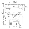
図1に示す本発明の実施形態の装置1は、本発明のさまざまな機能構成要素を強調するように示される。
【0018】
電力増幅器2は増幅する入力信号Sinを受信する。この信号は上流のプロセッサブロックから送信される。例えば、移動体電話機の場合、音声波形式の音声はアナログ信号に変換され、次いでディジタル信号に変換される。ディジタル信号は変調され、次いで周波数転位を経てベースバンド信号を高周波に載せる。上記のように、この信号は端末と通信中の基地局(図示せず)によって受信可能なように電力増幅を行なう必要がある。
【0019】
前記増幅器の出力信号Soutは、前記基地局と通信するアンテナ3に加えられる。
【0020】
出力信号Soutはまた、前記出力信号Soutを送達する前記増幅器の出力6を介してループ4(分岐線の1つで)にも加えられる。
【0021】
前記ループ4はまた、前記増幅器のバイアス電圧制御を受け入れる前記増幅器の入力5にも接続されている。
【0022】
ポイント6を介して前記ループに入力される前記信号Soutは、前記増幅器2によって出力される電力を検出する検出回路7に加えられる。前記検出回路は、第1に加算回路8の出力に、第2にマイクロコントローラ9に接続される。前記マイクロコントローラ9の機能については後述する。前記加算回路の別の入力は、減衰回路R1C1を含む調整回路10の出力から送信された信号を受信する。
【0023】
前記加算回路の入力端子の電圧を加算する前記加算回路の出力は、従来の比較器ブロック11の第1の入力に接続される。従来技術では、このブロックは2つの抵抗器Rを含み、その一方は前記入力と演算増幅器12の入力端子の1つに接続され、他方の抵抗器Rはコンデンサ13’に接続される。前記コンデンサの他端は前記演算増幅器12の出力に接続される。前記増幅器の他方の入力端子はグランドに接続される。第2の抵抗器の他端はブロック11の第2の入力端子に接続される。この第2の入力端子はディジタル/アナログ変換器14の出力に接続され、前記ディジタル/アナログ変換器14の入力は前記マイクロコントローラ9の出力に接続される。前記マイクロコントローラはまたメモリ15に接続される。
【0024】
前記増幅器12の出力は前記比較器ブロック11の出力13に接続される。この出力は第1に前記回路10の入力に接続され、第2に前記電力増幅器2のバイアス電圧制御入力5に接続される。
【0025】
本発明の装置1は以下のように動作する。
【0026】
本発明の装置を含む端末が送信モードの場合、増幅する信号Sinが前記電力増幅器2の入力に提供される。前記電力増幅器はこの信号をバースト方式で(特に過熱を回避するために)増幅する。仕様では前記電力の時間変化の下限値と上限値を規定しており、それが仕様の特性を形成している。
【0027】
前記端末が例えば33dBmの電力で信号を送信する場合、前記検出回路7は前記信号Soutを監視して前記マイクロコントローラ9に供給する。前記メモリ15は複数の電力レベルをそれぞれの複数のディジタル値に適合させる対応表をさらに含む。したがって、この場合、送信する33dBmの電力は所定のディジタル値に対応する。この値は、前記比較器ブロック11の入力端子の1つに基準電圧Vrefを加える前記変換器14によって、基準アナログ信号に変換される。
【0028】
前記比較器ブロック11の他方の入力端子の電圧VpeがVrefより小さい限り、前記ブロック11は、前記電力増幅器2のバイアス電圧と前記ブロック10の端子電圧に作用するように、出力13に増加する正の電圧Vcontを送達する。前記ブロック10と前記電力増幅器2の応答時間を考えると、下記の様に、前記ブロック10は最初に基準電圧Vcontに応答し(前記ブロック10の方が応答が速くVattが最初に変化する)、その後、前記増幅器2が前記基準電圧に応答する(前記増幅器2の方が応答が遅く、Vdetが続いて変化する)。したがって、応答Vpeは最初はVattの影響下で応答時間と共に変化し、その後はVdet+Vattの累積的な影響下で変化して、Vrefに達する。
【0029】
上記のように、従来技術では、前記比較器ブロック11のみがループ内に配置されて所望の電力レベルを調整していた。ただし、その従来技術の構成では、前記ブロック11は前記電力増幅器の出力信号Soutによる制御を専ら受ける。本出願の序論に鑑み、前記電力増幅器は周波数応答および/または時間応答が変化する能動構成要素を含むので、前記電力増幅器の応答が十分に速くない場合、出力信号は前記ブロック11を十分に速く制御できない。
【0030】
本発明では、この問題を、追加の電圧を前記加算回路8に送出して電圧Vpeがより迅速にまた前記増幅器2内の能動構成要素から独立して増大するように構成された、時間定数
【数1】
![]()
【0031】
その結果、前記比較器11によって出力される前記電圧Vcontも電圧Vattを伴わない電圧Vdetと比較して増大され、前記電力増幅器をセルR1C1が存在しない場合よりも大きく増幅させる、電力の増加した信号Soutを出力する。
【0032】
図2はそのような回路の利点を示す。この図は、安定状態に達するまで前記電力増幅器が入力信号を送信する初期段階に、前記3種類の電圧Vdet、Vatt、およびVpeが変化する様子を示す。前記電力増幅器の出力で検出された前記電圧Vdetが変化する様子を示す第1の曲線16が図示されている。第2の曲線17はセルR1C1の前記電圧Vattの変化の様子を示し、曲線16よりも速い時間応答で増加することが分かる。その結果、曲線18で表される残りの2つの電圧の総計である前記電圧Vpeは、Vattがない場合と比較してはるかに迅速に増加する。これはセルR1C1を追加したためで、以下のように記述できる新規の総合伝達関数から理解できる。
【数2】

本発明が上記の実施形態に限定されないのは言うまでもない。したがって、積分回路R1C1の代わりに、またはこれに加えて、抵抗器ブリッジを使用できる。装置1はグループに属するディジタル装置(移動体電話機、ディジタルパーソナルアシスタント、携帯型コンピュータ)内に統合されるように特に構成されている。
【図面の簡単な説明】
【図1】本発明の装置の一実施形態を示す図である。
【図2】調整手段の各端子間の電圧と、増幅器の各端子間電圧を、調整手段のある場合とない場合に分けて示す曲線をプロットした図である。
【符号の説明】
1 装置
2 電力増幅器
3 アンテナ
4 ループ
6 増幅器の出力
7 検出回路
8 加算回路
9 マイクロコントローラ
10 調整回路
11 比較器ブロック
12 演算増幅器
13 比較器ブロック11の出力
13’ コンデンサ
14 ディジタル/アナログ変換器
15 メモリ[0001]
BACKGROUND OF THE INVENTION
The present invention relates to the field of radio frequency signal transmission. More specifically, the present invention is an apparatus for transmitting a radio frequency signal, the power amplifying means for amplifying the power of the radio frequency signal received at the input, and the power amplification by controlling the gain of the power amplifying means. And a gain control means for adjusting the gain so that the power of the output signal from the means approaches a desired nominal value.
[0002]
[Prior art]
In a communication system that connects a mobile terminal to a base station, it is necessary to guarantee a minimum quality of service. For example, when transmitting a digital signal, this condition requires that the binary error rate is always less than some specified percentage. In order to satisfy this condition at the time of reception, the signal-to-noise ratio of the received signal always reliably exceeds a predetermined value.
[0003]
[Problems to be solved by the invention]
The problem to be solved by the present invention is that the power resources for each call from the terminal to the base station corresponding to the terminal, the power is just enough for the signal-to-noise ratio to meet the specifications. It is a problem of assigning as follows. This ensures that the call has a quality of service that guarantees a binary error rate below a predetermined limit and avoids excessive power consumption. Since the amount of power available in the terminal is limited, the transmitted power needs to be just enough.
[0004]
The mobile terminal includes a power amplifier so that the power of a signal to be transmitted can be increased. When the specification is implemented, this power amplifier is used to transmit the signal at a power level sufficient for the corresponding base station to receive correctly during the call. For example, when the base station is away from the terminal and the base station receives little or no call information from the terminal, the base station transmits a signal at a higher level of power than determined by the base station. A message is transmitted to the terminal for transmission.
[0005]
For example, the correspondence table recorded in the memory of the terminal establishes a correspondence between the power level to be transmitted and a predetermined value. The signal to be transmitted is input to the power amplifier, and the loop then monitors the signal output by the power amplifier to compare the signal output with the predetermined value. Until this value is reached, the comparator acts on the power amplifier to cause the power amplifier to increase its output power.
[0006]
Unfortunately, the way in which a power amplifier increases its output power varies from amplifier to amplifier, depending on the specific components that make up the amplifier and drifts that may already be affected.
[0007]
Nevertheless, this condition must meet the timing characteristics specified in the specification and the upper limit of amplifier power increase. Therefore, if the increase is too slow, information may be lost, and if the increase in power is too fast, the power will occupy a large portion of the acceptable range, which will hinder calls of other terminals.
[0008]
Therefore, from the above, in the prior art terminal, the length of time required for the terminal to increase the power from the power amplifier is not only uncertain, but also ensures that it meets the required quality of service. May be too long.
[0009]
The object of the present invention is to solve the above-mentioned problems of the terminal, and the present invention follows the stimulation of the input signal at a given input of the power amplifier to quickly reach the desired power level.
[0010]
[Means for Solving the Problems]
For this purpose, the present invention is an apparatus for transmitting a radio frequency signal (S1), wherein the power amplifying means (2) for amplifying the power of the radio frequency signal (S1) received at the input, and the power amplifying means Gain control means (11) for controlling the gain to adjust the gain so that the power of the output signal (Sout) from the power amplification means approaches a desired nominal value, and the gain control means comprises the power The apparatus operates with a monitoring signal (Vpe) representing a measurement signal (Vdet) that provides output power from the power amplifying means to supply a gain control signal (Vcont) that controls fluctuations in gain of the amplifying means, In addition to the power amplifying means, there is further included adjustment means (10) for supplying an additional adjustment signal (Vatt) to the gain control signal (Vcont) in response to the gain control signal (Vcont). , Characterized in that suitable for the monitoring signal also representative of said adjustment signal (Vatt) (Vpe) that is responsive to said gain control means faster.
[0011]
Thus, the apparatus of the present invention comprising adjusting means other than the prior art adjusting loop and reacting more rapidly to the input signal to the power amplifier makes it possible to reach the desired transmission power level more quickly. The transfer function of the power amplifier is changed for this purpose.
[0012]
In one embodiment, the adjustment means includes only passive components. Therefore, although the response to the input signal stimulus hardly drifts, the normal control means has an active component whose active component is likely to cause the response to drift.
[0013]
In one embodiment, the adjusting means includes a resistor bridge.
[0014]
In one embodiment, the adjusting means includes an integrating RC circuit.
[0015]
In one embodiment, the device of the present invention is integrated into a digital device belonging to a group (mobile phone, digital personal assistant, portable computer).
[0016]
The present invention may be better understood by reading the following description and examining the accompanying drawings. Each figure is shown as non-limiting.
[0017]
DETAILED DESCRIPTION OF THE INVENTION
The apparatus 1 of the embodiment of the present invention shown in FIG. 1 is shown to emphasize various functional components of the present invention.
[0018]
The power amplifier 2 receives an input signal Sin to be amplified. This signal is transmitted from an upstream processor block. For example, in the case of a mobile phone, voice waveform type voice is converted into an analog signal and then converted into a digital signal. The digital signal is modulated and then subjected to frequency transposition to place the baseband signal on a high frequency. As described above, this signal needs to be amplified so that it can be received by a base station (not shown) communicating with the terminal.
[0019]
The amplifier output signal Sout is applied to an antenna 3 that communicates with the base station.
[0020]
The output signal Sout is also applied to the loop 4 (at one of the branch lines) via the output 6 of the amplifier delivering the output signal Sout.
[0021]
The loop 4 is also connected to an
[0022]
The signal Sout input to the loop via point 6 is applied to a detection circuit 7 that detects the power output by the amplifier 2. The detection circuit is connected first to the output of the adder circuit 8 and secondly to the microcontroller 9. The function of the microcontroller 9 will be described later. Another input of the summing circuit receives a signal transmitted from the output of the adjusting
[0023]
The output of the adder circuit for adding the voltages at the input terminals of the adder circuit is connected to the first input of the
[0024]
The output of the
[0025]
The device 1 of the present invention operates as follows.
[0026]
When the terminal including the device of the present invention is in the transmission mode, a signal Sin to be amplified is provided to the input of the power amplifier 2. The power amplifier amplifies this signal in a burst manner (especially to avoid overheating). The specification defines a lower limit value and an upper limit value of the time variation of the power, which form the characteristics of the specification.
[0027]
When the terminal transmits a signal with power of, for example, 33 dBm, the detection circuit 7 monitors the signal Sout and supplies it to the microcontroller 9. The
[0028]
As long as the voltage Vpe of the other input terminal of the
[0029]
As described above, in the prior art, only the
[0030]
In the present invention, this problem, which is configured to increase independently additional voltage from the active component of the adding circuit 8 sends more quickly or in the amplifier 2 is voltage Vpe by the time constant [ Number 1]
![]()
[0031]
As a result, the said voltage Vcont output by the
[0032]
FIG. 2 illustrates the advantages of such a circuit. This figure shows how the three types of voltages Vdet, Vatt, and Vpe change during an initial stage in which the power amplifier transmits an input signal until a stable state is reached. A
[Expression 2]
Needless to say, the present invention is not limited to the above-described embodiment. Therefore, a resistor bridge can be used instead of or in addition to the integrating circuit R1C1. The device 1 is particularly configured to be integrated into a digital device (mobile phone, digital personal assistant, portable computer) belonging to a group.
[Brief description of the drawings]
FIG. 1 shows an embodiment of the apparatus of the present invention.
FIG. 2 is a graph plotting curves showing voltages between terminals of an adjusting unit and voltages between terminals of an amplifier separately with and without the adjusting unit.
[Explanation of symbols]
DESCRIPTION OF SYMBOLS 1 Device 2 Power amplifier 3 Antenna 4 Loop 6 Amplifier output 7 Detection circuit 8 Addition circuit 9
Claims (5)
入力で前記制御信号(Vcont)を受け取り、調整信号(Vatt)を供給する調整手段(10)と、
測定信号(Vdet)および調整信号(Vatt)を加算して得られる前記監視信号(Vpe)を供給する加算手段(8)とを備えており、
前記調整手段(10)は、前記監視信号(Vpe)が迅速に増大して前記制御手段(11)に入力するように、前記電力増幅手段(2)の応答時間よりも短い応答時間を有するものであることを特徴とする、前記装置。An apparatus for transmitting a radio frequency signal, the power amplifying means (2) for amplifying the power of the radio frequency signal (Sin) received at the input, and controlling the gain of the power amplifying means (2) to thereby amplify the power For an input (5) that controls the bias voltage of the power amplification means (2) to adjust the gain so that the power of the output signal (Sout) of the means (2) approaches the desired nominal value (Vref) And a control means (11) for supplying a control signal (Vcont). The control means (11) outputs a monitoring signal (Vpe) obtained from a measurement signal (Vdet) of the output power of the power amplification means. Operative to provide the control signal (Vcont) for controlling the gain variation of the power amplification means compared to the desired nominal value (Vref), the device further comprising:
An adjusting means (10) for receiving the control signal (Vcont) at an input and supplying an adjustment signal (Vatt);
Adding means (8) for supplying the monitoring signal (Vpe) obtained by adding the measurement signal (Vdet) and the adjustment signal (Vatt);
The adjusting means (10) has a response time shorter than the response time of the power amplifying means (2) so that the monitoring signal (Vpe) increases rapidly and is input to the control means (11). The device as described above.
Applications Claiming Priority (2)
| Application Number | Priority Date | Filing Date | Title |
|---|---|---|---|
| FR0106072 | 2001-05-07 | ||
| FR0106072A FR2824433B1 (en) | 2001-05-07 | 2001-05-07 | DEVICE FOR REGULATING THE CONTROL OF THE POWER OF A TRANSMITTER |
Publications (3)
| Publication Number | Publication Date |
|---|---|
| JP2002344267A JP2002344267A (en) | 2002-11-29 |
| JP2002344267A5 JP2002344267A5 (en) | 2009-04-16 |
| JP4298961B2 true JP4298961B2 (en) | 2009-07-22 |
Family
ID=8863044
Family Applications (1)
| Application Number | Title | Priority Date | Filing Date |
|---|---|---|---|
| JP2002123521A Expired - Fee Related JP4298961B2 (en) | 2001-05-07 | 2002-04-25 | Adjustment device for controlling the power of the transmitter |
Country Status (9)
| Country | Link |
|---|---|
| US (1) | US6603350B2 (en) |
| EP (1) | EP1257054B1 (en) |
| JP (1) | JP4298961B2 (en) |
| CN (1) | CN1230022C (en) |
| AT (1) | ATE348447T1 (en) |
| DE (1) | DE60216660T2 (en) |
| ES (1) | ES2278884T3 (en) |
| FR (1) | FR2824433B1 (en) |
| PT (1) | PT1257054E (en) |
Families Citing this family (3)
| Publication number | Priority date | Publication date | Assignee | Title |
|---|---|---|---|---|
| US7116088B2 (en) * | 2003-06-09 | 2006-10-03 | Silicon Storage Technology, Inc. | High voltage shunt regulator for flash memory |
| GB2414352A (en) * | 2004-05-18 | 2005-11-23 | Roke Manor Research | An adaptively-corrected RF pulse amplifier for a beam-steered radar antenna array |
| CN114614840B (en) * | 2022-03-08 | 2023-08-25 | 福耀玻璃工业集团股份有限公司 | Signal amplifier, system and signal transmission method for vehicle |
Family Cites Families (7)
| Publication number | Priority date | Publication date | Assignee | Title |
|---|---|---|---|---|
| FI87028C (en) * | 1989-12-22 | 1992-11-10 | Nokia Mobile Phones Ltd | METHOD OF RESULT OF EFFECTIVE PROCEDURE WITHOUT SPREADING OF EFFECTIVE EFFECTS AND COVERING OF METHODS |
| US5150075A (en) * | 1991-06-03 | 1992-09-22 | Motorola, Inc. | Power amplifier ramp up method and apparatus |
| JP3180424B2 (en) * | 1992-03-11 | 2001-06-25 | ソニー株式会社 | Output control circuit |
| US5642075A (en) * | 1995-12-21 | 1997-06-24 | Itt Corporation | Sampled data automatic gain control |
| JPH09331222A (en) * | 1996-06-11 | 1997-12-22 | Nec Corp | Correcting device for gain control signal |
| DE19702280A1 (en) * | 1997-01-23 | 1998-07-30 | Bosch Gmbh Robert | Power gain control method |
| US6307429B1 (en) * | 2000-01-12 | 2001-10-23 | National Semiconductor Corporation | Extended power ramp table for power amplifier control loop |
-
2001
- 2001-05-07 FR FR0106072A patent/FR2824433B1/en not_active Expired - Fee Related
-
2002
- 2002-04-15 DE DE60216660T patent/DE60216660T2/en not_active Expired - Lifetime
- 2002-04-15 ES ES02290938T patent/ES2278884T3/en not_active Expired - Lifetime
- 2002-04-15 AT AT02290938T patent/ATE348447T1/en not_active IP Right Cessation
- 2002-04-15 EP EP02290938A patent/EP1257054B1/en not_active Expired - Lifetime
- 2002-04-15 PT PT02290938T patent/PT1257054E/en unknown
- 2002-04-24 US US10/128,567 patent/US6603350B2/en not_active Expired - Lifetime
- 2002-04-25 JP JP2002123521A patent/JP4298961B2/en not_active Expired - Fee Related
- 2002-04-29 CN CNB021188262A patent/CN1230022C/en not_active Expired - Fee Related
Also Published As
| Publication number | Publication date |
|---|---|
| ATE348447T1 (en) | 2007-01-15 |
| EP1257054A3 (en) | 2004-09-08 |
| FR2824433B1 (en) | 2003-08-01 |
| DE60216660T2 (en) | 2007-10-18 |
| US20020171482A1 (en) | 2002-11-21 |
| EP1257054B1 (en) | 2006-12-13 |
| FR2824433A1 (en) | 2002-11-08 |
| CN1230022C (en) | 2005-11-30 |
| ES2278884T3 (en) | 2007-08-16 |
| EP1257054A2 (en) | 2002-11-13 |
| PT1257054E (en) | 2007-03-30 |
| JP2002344267A (en) | 2002-11-29 |
| CN1384687A (en) | 2002-12-11 |
| US6603350B2 (en) | 2003-08-05 |
| DE60216660D1 (en) | 2007-01-25 |
Similar Documents
| Publication | Publication Date | Title |
|---|---|---|
| CA2086541C (en) | Power amplifier saturation detection and correction method and apparatus | |
| EP0740422B1 (en) | Power control circuit for transmission apparatus | |
| AU697823B2 (en) | Radio frequency transceiver system for digital communication | |
| JP2910242B2 (en) | Power amplifier ramp-up method and apparatus | |
| EP1190502B1 (en) | Adjusting maximum transmit power to maintain constant margin for adjacent channel power rejection | |
| TW535368B (en) | System for closed loop power control using a linear or a non-linear power amplifier | |
| EP0416613A2 (en) | Transmission power control circuit | |
| JP3358598B2 (en) | Transmission power correction circuit | |
| JP4298961B2 (en) | Adjustment device for controlling the power of the transmitter | |
| US7110724B1 (en) | System and method for detecting compression of a power amplifier circuit | |
| JP2003037640A (en) | Transmitting circuit for radio communication equipment | |
| JP4023025B2 (en) | Wireless communication apparatus and transmission power control method for wireless communication apparatus | |
| EP1120902A2 (en) | Transmitter and mobile station | |
| KR20060032287A (en) | Apparatus and method for compensating rf transmission power in the mobile communication terminal | |
| JP3320427B2 (en) | Power control device | |
| KR200368938Y1 (en) | Apparatus for control transmission power of mobile terminal | |
| KR20000046227A (en) | Apparatus and method for setting up initial transmitting power of portable wireless terminal | |
| JP2003258652A (en) | Power servo-loop, rf signal amplifier circuit, and rf signal transmitter having such circuit | |
| JPH0927723A (en) | Transmitted electric power control system | |
| JP2001028552A (en) | Direct conversion receiver | |
| JPS59212035A (en) | Transmission output controlling circuit | |
| JPH06260958A (en) | Automatic electric power control circuit and radio communications equipment | |
| JPH07254880A (en) | Correcting circuit for transmission output level of terminal unit of mobile communication | |
| JPH0653764A (en) | Power controller | |
| JP2000324187A (en) | Device for controlling transmission power |
Legal Events
| Date | Code | Title | Description |
|---|---|---|---|
| A621 | Written request for application examination |
Free format text: JAPANESE INTERMEDIATE CODE: A621 Effective date: 20050407 |
|
| A977 | Report on retrieval |
Free format text: JAPANESE INTERMEDIATE CODE: A971007 Effective date: 20071210 |
|
| A131 | Notification of reasons for refusal |
Free format text: JAPANESE INTERMEDIATE CODE: A131 Effective date: 20071218 |
|
| A601 | Written request for extension of time |
Free format text: JAPANESE INTERMEDIATE CODE: A601 Effective date: 20080312 |
|
| A602 | Written permission of extension of time |
Free format text: JAPANESE INTERMEDIATE CODE: A602 Effective date: 20080317 |
|
| A521 | Request for written amendment filed |
Free format text: JAPANESE INTERMEDIATE CODE: A523 Effective date: 20080618 |
|
| A131 | Notification of reasons for refusal |
Free format text: JAPANESE INTERMEDIATE CODE: A131 Effective date: 20080715 |
|
| A601 | Written request for extension of time |
Free format text: JAPANESE INTERMEDIATE CODE: A601 Effective date: 20081009 |
|
| A602 | Written permission of extension of time |
Free format text: JAPANESE INTERMEDIATE CODE: A602 Effective date: 20081015 |
|
| A521 | Request for written amendment filed |
Free format text: JAPANESE INTERMEDIATE CODE: A523 Effective date: 20090115 |
|
| A524 | Written submission of copy of amendment under article 19 pct |
Free format text: JAPANESE INTERMEDIATE CODE: A524 Effective date: 20090115 |
|
| TRDD | Decision of grant or rejection written | ||
| A01 | Written decision to grant a patent or to grant a registration (utility model) |
Free format text: JAPANESE INTERMEDIATE CODE: A01 Effective date: 20090331 |
|
| A01 | Written decision to grant a patent or to grant a registration (utility model) |
Free format text: JAPANESE INTERMEDIATE CODE: A01 |
|
| A61 | First payment of annual fees (during grant procedure) |
Free format text: JAPANESE INTERMEDIATE CODE: A61 Effective date: 20090416 |
|
| R150 | Certificate of patent or registration of utility model |
Free format text: JAPANESE INTERMEDIATE CODE: R150 |
|
| FPAY | Renewal fee payment (event date is renewal date of database) |
Free format text: PAYMENT UNTIL: 20120424 Year of fee payment: 3 |
|
| FPAY | Renewal fee payment (event date is renewal date of database) |
Free format text: PAYMENT UNTIL: 20130424 Year of fee payment: 4 |
|
| FPAY | Renewal fee payment (event date is renewal date of database) |
Free format text: PAYMENT UNTIL: 20140424 Year of fee payment: 5 |
|
| R250 | Receipt of annual fees |
Free format text: JAPANESE INTERMEDIATE CODE: R250 |
|
| R250 | Receipt of annual fees |
Free format text: JAPANESE INTERMEDIATE CODE: R250 |
|
| R250 | Receipt of annual fees |
Free format text: JAPANESE INTERMEDIATE CODE: R250 |
|
| R250 | Receipt of annual fees |
Free format text: JAPANESE INTERMEDIATE CODE: R250 |
|
| LAPS | Cancellation because of no payment of annual fees |