JP4290320B2 - Routing device - Google Patents
Routing device Download PDFInfo
- Publication number
- JP4290320B2 JP4290320B2 JP2000295841A JP2000295841A JP4290320B2 JP 4290320 B2 JP4290320 B2 JP 4290320B2 JP 2000295841 A JP2000295841 A JP 2000295841A JP 2000295841 A JP2000295841 A JP 2000295841A JP 4290320 B2 JP4290320 B2 JP 4290320B2
- Authority
- JP
- Japan
- Prior art keywords
- data
- routing
- key data
- line
- main control
- Prior art date
- Legal status (The legal status is an assumption and is not a legal conclusion. Google has not performed a legal analysis and makes no representation as to the accuracy of the status listed.)
- Expired - Fee Related
Links
Images


Classifications
-
- H—ELECTRICITY
- H04—ELECTRIC COMMUNICATION TECHNIQUE
- H04L—TRANSMISSION OF DIGITAL INFORMATION, e.g. TELEGRAPHIC COMMUNICATION
- H04L45/00—Routing or path finding of packets in data switching networks
-
- H—ELECTRICITY
- H04—ELECTRIC COMMUNICATION TECHNIQUE
- H04L—TRANSMISSION OF DIGITAL INFORMATION, e.g. TELEGRAPHIC COMMUNICATION
- H04L45/00—Routing or path finding of packets in data switching networks
- H04L45/54—Organization of routing tables
-
- H—ELECTRICITY
- H04—ELECTRIC COMMUNICATION TECHNIQUE
- H04L—TRANSMISSION OF DIGITAL INFORMATION, e.g. TELEGRAPHIC COMMUNICATION
- H04L45/00—Routing or path finding of packets in data switching networks
- H04L45/60—Router architectures
-
- H—ELECTRICITY
- H04—ELECTRIC COMMUNICATION TECHNIQUE
- H04L—TRANSMISSION OF DIGITAL INFORMATION, e.g. TELEGRAPHIC COMMUNICATION
- H04L45/00—Routing or path finding of packets in data switching networks
- H04L45/74—Address processing for routing
- H04L45/745—Address table lookup; Address filtering
- H04L45/7453—Address table lookup; Address filtering using hashing
-
- H—ELECTRICITY
- H04—ELECTRIC COMMUNICATION TECHNIQUE
- H04L—TRANSMISSION OF DIGITAL INFORMATION, e.g. TELEGRAPHIC COMMUNICATION
- H04L49/00—Packet switching elements
- H04L49/30—Peripheral units, e.g. input or output ports
- H04L49/3009—Header conversion, routing tables or routing tags
-
- H—ELECTRICITY
- H04—ELECTRIC COMMUNICATION TECHNIQUE
- H04L—TRANSMISSION OF DIGITAL INFORMATION, e.g. TELEGRAPHIC COMMUNICATION
- H04L12/00—Data switching networks
- H04L12/54—Store-and-forward switching systems
- H04L12/56—Packet switching systems
- H04L12/5601—Transfer mode dependent, e.g. ATM
- H04L2012/5619—Network Node Interface, e.g. tandem connections, transit switching
- H04L2012/562—Routing
Landscapes
- Engineering & Computer Science (AREA)
- Computer Networks & Wireless Communication (AREA)
- Signal Processing (AREA)
- Data Exchanges In Wide-Area Networks (AREA)
- Communication Control (AREA)
Description
【0001】
【発明の属する技術分野】
本発明はInternet, ATM network等におけるルーチング処理に際してCAM(Content Addressable Memory)を使用するルーチング装置に係わり、特に、回線より到来するパケットの宛先アドレスに応じたルーチングデータをCAMより求めてパケットに付加し、該ルーチングデータに基づいてパケットをスイッチングして所定の回線に送出するルーチング装置に関する。
【0002】
【従来の技術】
昨今のInternet/ATM networkの爆発的な普及により、ルータ(router)/ATM交換機(ATM switch)の処理速度は高速化の一途をたどっている。また、回線の高集積化によりそのルーチング/スイッチングに必要となるデータ(ルーチングデータ)を検索するためのテーブルも大容量化してきている。
ルーチングデータの検索法はCAM(Content Addressable Memory)を使用した変換処理技術により達成されている。しかし、CAMは大容量化に伴い、従来の容量のものでは多数のテーブルが必要になり、通常のLSI内部に実装することが難しくなっている。又、大容量のものは、専用の LSIとして市販されるようになっている。
【0003】
図15は従来のルータの概略構成図であり、一般的なルータにおけるCAMを使用した検索方法の概要を説明するものである。1は主制御部(CPU)、2はスイッチ部、31〜3n,41〜4mは回線とスイッチ間に設けられた回線カードである。回線におけるデータ伝送はPOS(Packet over SONET,Packet over SDH)を使った伝送が一般的であり、このPOSではSDH,SONETのペイロード部にIPパケットをマッピングして伝送する。図示しない回線終端部はPOS回線よりIPパケットを分離して、回線カード31〜3nに入力する。各回線カード31〜3nのパケットプロセッサ3aはIPパケットの宛先アドレスを抽出し、該宛先アドレスに応じたルーチングデータをCAM 3bより取得し、該ルーチングデータをパケットに付加してスイッチ2に入力する。スイッチ2は各回線カード31〜3nから入力するルーチングデータ付きパケットを該ルーチングデータに基づいてスイッチングして別の回線カード41〜4mに入力する。回線カード41〜4mのパケットプロセッサはルーチングデータを取り除き、しかる後、パケットをSDH,SONETフレームのペイロードにマッピングしてPOS回線に送出する。
【0004】
図16はCAM 3bをCAM LSI 3b1と連想メモリ3b2に分離して示す回線カードの構成図、図17はCAM検索の流れ図である。CAM LSI 3b1のキーデータ記憶部(図示せず)は多数の宛先アドレスに応じたキーデータを記憶し、又、連想メモリ3b2はルーチングデータを記憶する。IPパケットのIPヘッダは宛先アドレスDA(destination address=IP address)を有しているから、回線カード31〜3nのパケットプロセッサ3aはIPパケットが入力すると(ステップ101)、該入ってきたIPパケットより宛先アドレスDAを抽出し(ステップ102)、該宛先アドレスをキーデータ(key data)として、予め変換テーブルを有するCAM 3bに転送する。CAM 3bのCAM LSI 3b1はこのキーデータに対応するIP addressがキーデータ記憶部に存在するかチェックし、存在すれば、該キーデータを前記連想メモリのアドレスに変換して連想メモリ3b2に送出する(ステップ103)。RAM構成の連想メモリ3b2は、入力したアドレスをもとにあらかじめ設定された連想データ、例えば、スイッチングに必要となるハイウェイ番号HW-No.(Highway No.)を出力する。パケットプロセッサ3aは、IPパケットを出力する直前に該ハイウェイ番号HW_No.をパケットに付与してスイッチ部2に入力し、スイッチはハイウェイ番号HW_No.によりルーチング動作を行なう(ステップ104)。
【0005】
図18は従来のルータの詳細な構成図であり、図15〜図17と同一部分には同一符号を付している。主制御部1,1′は信頼性をあげるために二重化されており、同一の構成を備えている。すなわち、主制御部1,1′は、▲1▼メインプロセッサMPU 1a,1a′、▲2▼メインメモリMM 1b,1b′、▲3▼キャッシュメモリ(図示せず)、▲4▼各種I/OやCAM等のデバイスをメインプロセッサMPUに接続するためのMPU bus変換ブリッジ1c,1c′、▲5▼メインプロセッサが隣接するルータとの間で通信を行う際の出力ポート検索用CAM 1d,1d′、▲6▼スイッチ2とは別線にて各回線カード31〜3nへ主制御部が作成したルーチングテーブルを転送するためのイーサネットスイッチングハブ(Ethernet Switching HUB)1e,1e′、▲7▼回線カードからスイッチ経由で到来する自局宛パケットをメインプロセッサ MPUに送出するためのMPU bus変換ブリッジ1f,1f′などを有している。
【0006】
回線カード31〜3nはSONET/SDH等の各種回線を収容するもので、同一の構成を備えている。ただし、回線カードが収容する各回線の速度は同一であるが、回線速度は回線カード毎に異なっている。パケットプロセッサ3aは、(1) POS回線等を介して到来するパケットの宛先アドレスDAを抽出し、該宛先アドレスDAをルーチングデータ検索用のキーデータとしてCAMへ送出したり、(2) パケットにルーチングデータ(ハイウェイ番号HW_No.)を付与してスイッチに送出したり、(3) スイッチングされたパケットよりルーチングデータを削除して回線へ送出する。CAM 3bはCAM LSIおよび連想メモリを備え、キーデータとして入力される宛先アドレスDAよりルーチングデータ(ハイウェイ番号HW_No.)を求めたり、その逆を実行する。LAN制御部(LANC:Lan controllor)3cはメインプロセッサ MPUとの間で通信を行なってルーチングテーブルを受信する。ローカルのプロセッサMPUはLAN制御部3cの制御、回線カード内部の各種設定(Configuration)制御を行う。
スイッチ2は回線カードと主制御部1,1′間でのパケットの交換制御を行なうと共に、各回線カード間でのパケットの交換制御を行なう。
【0007】
図19は従来のルータ装置のパケットの流れを示す説明図である。
1)POS回線から入力されたデータパケットは、回線カード3内の入力部分でパケットに分離される。
2) パケットプロセッサ3aはパケットヘッダ内のIP宛先アドレスDAに基づいてCAM 3bからハイウェイ番号HW-No.、その他必要な情報α(QOS情報、フィルタリング情報など)を検索し、パケット(payload部分)にこれらHW-No.+αを付加してスイッチ2に転送する。
3) スイッチ2はルーチングデータHW-No.+αによりパケットをスイッチングして出側の回線カード4に入力する。回線カード4のパケットプロセッサ4aはスイッチより入力するパケットからルーチングデータHW_No.+αを取り除く。
4) ついで、パケットプロセッサ4aは最終的にパケットをSDH,SONETフレームのペイロードにマッピングしてPOS回線に送出する。以上により全てのルーチング処理が完了する。
【0008】
図20はCAM LSIの概略内部構造図である。CAM LSI 3b1は、アドレスデコーダ5a、メモリアレイ5b、インデックスレジスタ5c、マスクレジスタ5d、レスポンスレジスタ5e、プライオリティエンコーダ5fを有している。
アドレスデコーダ5aはアドレスデータをデコードし、別途入力するキーデータをメモリアレイの所定アドレスに格納し、あるいはメモリアレイよりキーデータを読出して出力する。メモリアレイ5bは多数の宛先アドレスに応じたキーデータを格納し、インデックスレジスタ5cは検索したいキーデータ(検索キーデータ)、すなわち、POS回線から受信したパケットの宛先アドレスに応じたキーデータを格納する。マスクレジスタ5dは検索キーデータのうちマスクするビット位置を指定する("1"でマスク)。レスポンスレジスタ5eは、(1) メモリアレイ5bに記憶されているキーデータと検索キーデータとのマッチング結果(比較結果)、あるいは、(2) メモリアレイ5bに記憶されているキーデータと検索キーデータの非マスク部分とのマッチング結果を格納する。プライオリティエンコーダ5fはレスポンスレジスタ5eのマッチング結果をもとに連想メモリ3b2のアドレスを生成する。連想メモリ3b2は入力するアドレスより連想データ(ルーチングデータ+α)を出力する。
【0009】
尚、図20ではキーデータを8ビットとして示しているが、説明の都合によるもので実際にはキーデータは32ビット等である。又、メモリアレイ5が8個のキーデータを記憶する場合を示しているが、メモリアレイは実際には非常に多くのキーデータを記憶する容量を有している。又、CAM内部のメモリアレイ5bは、CAM検索の用途に応じてビット幅が可変設定できるようになっており、メモリアレイの構成を変更するレジスタ(図示せず)を具備するが、連想メモリ 3b2については、ハードウェア設計時に連想用アドレスと連想データのビット幅が固定される。
【0010】
【発明が解決しようとする課題】
従来のCAMを用いたルーチング装置(ルータ)では、下記の問題がある。
1) CAM LSIのハイコスト
昨今のInternetの普及により、CAMのエントリ数が増加の一途をたどっている。CAM LSI一個当りで処理できるエントリ数は、1エントリ当り36ビット必要とすると、せいぜい64k個程度である。ここで36ビットは、IP_v4(IP-version 4)における宛先アドレスとして必要な32ビットと制御ビットとしての4ビットの合計である。
【0011】
2) CAM LSIの高い実装面占有率
上記のようにCAM LSI(4×4cm程度)として15個搭載する必要があるとすると、実装面占有率が高くなる。このため、回路カードを二階建て等の複雑な構造にしなければならなくなる。
3) ルーチングテーブルの転送時間
ルーチングテーブルを一元管理する主制御部のメインプロセッサから各回線カードへルーチングテーブルを転送する必要がある。例えば、システム立ち上げの際、各回線カード内に実装しているCAM へ主制御部のメインプロセッサからルーチングテーブルを転送する必要がある。このため、システム立ち上げに相当の時間がかかり、しかも、障害発生時のリカバリーにも時間がかかる。
【0012】
4) 連想データのビット幅変更
CAMは、CAM LSIにRAM構成の連想メモリを外付けする構成になっている。このため、キーデータがIP_v4→IP_v6(4バイト→16バイト)等へ変更になると、ハードウェアの回路構成を変更する必要が発生し、新規回線カードを設計しなおさなければならない。
5) キーデータのマルチプルヒット(Multiple hit)
従来のCAMは統計処理機能がないため、検索キーデータに複数のエントリキーデータがヒットするマルチプルヒット(Multiple hit)時に統計処理を実行できない。このため、主制御部のメインプロセッサMPUがメインメモリMM上でプログラム処理により統計情報を計算する必要がある。この統計処理はメインプロセッサに対し高負荷となる。
【0013】
6) 回線速度とCAMの関係
従来のルータは回線カードにCAMを実装し、かつ、回線カードには同一速度の複数の回線を収容する(例えば、OC-12回線×4を搭載する)。このようにする理由は、回線カードに速度が異なる回線を収容する構成では、全ての回線カードに最高速度の高価なCAMを必要とし、コストアップになるからである。しかし、回線カード毎に同一速度の回線を収容する従来構成のルータでは、各回線速度に応じた回線カードを用意する必要が有り、ネットワークによっては使用しない回線カードが発生したり、回線カードに収容する回線数が少ない場合が発生する。すなわち、従来のルーチング装置は回線カードの回線収容効率が悪く、コストアップになっている。
【0014】
以上から本発明の目的は、安価で、かつ、コンパクトなルーチング装置を提供することである。
本発明の別の目的は、使用するCAMの個数を削減してルーチング装置のコストダウンと実装効率を高めることである。
本発明の別の目的は、障害が発生しても運用継続可能にしてルーチング装置の信頼性を向上することである。
本発明の別の目的は、CAM周辺の回路を設計変更しなくてもCAMにおける連想データやキーデータのビット幅を可変制御できるルーチング装置を提供することである。
本発明の別の目的は、マルチプルヒット時の処理をCAM LSI内部にて実現できるようにしてメインプロセッサの統計処理を少なくし、該メインプロセッサの負荷を軽減することである。
本発明の別の目的は、速度の異なるCAMを回線速度毎に使い分けれるようにし、かつ、回線カードに種々の回線速度の回線を収容できるようにして、ルーチング装置のコストダウンを図ることである。
本発明の別の目的は、電源投入時やリカバリー時におけるシステム立ち上げ時間を減少できるルーチング装置を提供することである。
【0015】
【課題を解決するための手段】
本発明は、回線より到来するパケットの宛先アドレスに応じたルーチングデータを求めて該パケットに付加し、ルーチングデータに基づいてパケットをスイッチングして所定の回線に送出するルーチング装置であり、(1) ルーチングデータ発生部を備え、要求された宛先アドレスに応じたルーチングデータを発生して要求元に送出する主制御部、(2) 回線より到来するパケットの宛先アドレスを抽出し、該宛先アドレスに応じたルーチングデータを通知するよう主制御部に要求し、主制御部より通知されたルーチングデータをパケットに付加して出力する回線インタフェース部、(3) 所定の回線インタフェース部から入力する前記ルーチングデータ要求を主制御部に送出し、主制御部からのルーチングデータを要求元の回線インタフェース部に送出し、ルーチングデータ付きパケットを該ルーチングデータに基づいてスイッチングして別の回線インタフェース部に送出するスイッチ部、を備えている。
【0016】
主制御部のルーチングデータ発生部は、(1) ルーチングデータを記憶する連想メモリ部、(2) 宛先アドレスをキーデータとするとき、多数の宛先アドレスであるキーデータを記憶するキーデータ記憶部、(3) 前記要求された宛先アドレスであるキーデータがキーデータ記憶部に存在するとき、該キーデータを前記連想メモリのアドレスに変換する変換部、(4) 連想メモリ部の該アドレスよりルーチングデータを読出して要求元である回線インタフェース部に送出するルーチングデータ送出部、を有している。
本発明のルーチング装置は、従来、個々の回線カードと主制御部の両方に配置していたCAM(ルーチングデータ発生部)を主制御部側に集約してルーチングテーブルを一元管理する。これにより、システム全体で使用しているCAMの個数を削減でき、コストダウンと実装効率を向上することができる。
又、CAMを主制御部にのみ持たせるだけでよいため、システム立ち上げの際、主制御部のメインプロセッサから回線カードにルーチングテーブルを転送する必要がなく、電源投入時やリカバリー時における立ちシステム上げ時間を減少することができる
【0017】
本発明のルーチング装置は、主制御部に各回線速度に対応させてルーチングデータ発生部(CAM)をそれぞれ備える。主制御部は、回線インタフェース部から回線識別子付きのルーチングデータ要求があったとき、回線速度に応じたCAMからルーチングデータを求めて要求元の回線インタフェース部に送出する。このようにすれば速度の異なるCAMを回線速度毎に使い分けることが可能となり、しかも、回線カードに種々の速度の回線を収容することが可能となり、安価で低速のCAMを使用でき、しかも、回線カードの回線収容効率を向上できるためルーチング装置のコストダウンを図ることができる。
【0018】
本発明のルーチング装置は、連想メモリ部とキーデータ記憶部を1つのメモリアレイで構成し、該メモリアレイの連続する2つの領域をそれぞれ連想メモリ部、キーデータ記憶部とする。メモリアレイに対するアクセス部は、メモリアレイの1バイトセルの総数をy、キーデータ幅をkバイト、ルーチングデータを含む連想データ幅をrバイトとするとき、登録可能なキーデータ数および連想データ数であるエントリ数eを次式
e=y/(k+r)
により演算し、これらk,r,eによりキーデータおよび連想データのメモリアレイへの読み/書き制御を行なう。このようにすれば、CAM周辺の回路を設計変更しなくても、y,k,rをプログラマブルに変更するだけで連想データやキーデータのビット幅を可変制御できる。
本発明のルーチング装置は、主制御部のルーチングデータ発生部にマルチプルヒットしたエントリ数、エントリキーデータの管理を行なわせる。このようにすれば、マルチプルヒット時の処理をCAM LSI内部にて実現でき、メインプロセッサの統計処理を少なくして負荷を軽減することができる。
【0019】
【発明の実施の形態】
(A)システム構成
図1は本発明のルーチング装置のシステム構成図であり、11、11′は信頼性をあげるために二重化された同一構成の主制御部(0系、1系の主制御部)、12はスイッチ部、131〜13nはSONET/SDH、Ethernet等の各種回線を収容する回線カード(回線インタフェース部)である。
主制御部11,11′は、▲1▼メインプロセッサMPU 11a,11a′、▲2▼メインメモリMM 11b,11b′、▲3▼システムバスに接続された各種I/OやCAM等のデバイスをメインプロセッサMPUに接続するためのMPUバス変換ブリッジ11c,11c′、▲4▼他系のCAMとの通信を行うためのクロスコネクト部11d,11d′、▲5▼回線速度対応に設けられ、回線速度によって選択可能な複数個のCAM11e1〜11en,11e1′〜11en′、▲6▼各回線カードからスイッチ経由で到来する自局宛データを取り込んでシステムバスに送出するバス変換ブリッジ11f,11f′などを有している。各回線カードやメインプロセッサMPUからCAMへのアクセスはすべてシステムバス11g,11g′を介して行われる。尚、11h、11h′はMPUバスである。
【0020】
CAM11e1〜11en,11e1′〜11en′は、(1) ルーチングデータを記憶する連想メモリ部21、(2) 宛先アドレスをキーデータとするとき、多数の宛先アドレスに応じたキーデータを記憶するキーデータ記憶部22、(3) 各回線カードから要求された宛先アドレスDAに応じたキーデータ(検索キーデータ)がキーデータ記憶部22に存在するとき、キーデータを連想メモリのアドレスに変換するアドレス変換部23、(4) 連想メモリ21の該アドレスよりルーチングデータを読出すメモリアクセス部24を備えている。各CAM11e1〜11en,11e1′〜11en′はブロック的に同一構成を備えているが、製造プロセスによりアクセス速度が異なり、サフィックス番号が大きくなる程、高速アクセス可能になっている。
【0021】
回線カード131〜13nは、パケットプロセッサ13a、回線カード内部の各種設定(Configuration)を行うマイクロプロセッサMPU 13bを備えている。パケットプロセッサ13aは、(1)各回線より到来するパケットの宛先アドレスDAを抽出し、該宛先アドレスDAをルーチングデータ検索用のキーデータ(検索キーデータ)としてスイッチ12を介して主制御部11,11′のCAMへ送出したり、(2) 主制御部11,11′よりスイッチ12を介して取得したルーチングデータ(ハイウェイ番号HW_No.)をパケットに付与してスイッチに送出したり、(3) スイッチングされて入力するパケットよりルーチングデータを削除して回線へ送出する機能を有している。尚、パケットプロセッサ13aは、スイッチが検索キーデータであるか、パケットであるかを識別できるようにするために、検索キーデータにキーフラグを付加し、パケットにはデータフラグを付加してスイッチ12に送出する。
スイッチ12は、(1) 所定の回線カード131〜13nから入力するキーフラグ付きの検索キーデータを主制御部11に送出し、(2) 主制御部11のCAMより求めたルーチングデータを要求元の回線カードに送出し、又、(3) データフラグ付きのパケットをルーチングデータに基づいてスイッチングして別の回線インタフェース部に送出する。
【0022】
図1のルーチング装置は、以下の特徴を有している。
1) CAM 実装位置
従来個々の回線カードと主制御部の両方に配置していた各CAMを主制御部11側に集約し、ルーチングデータ要求、検索されたルーチングデータの送受を、パケットプロセッサ13aとスイッチ12のパスを経由するin-band方式により行なう。また、ルーチングテーブル(キーデータ/連想データ)を主制御部11のCAMで一元管理し、従来各回線カードで重複管理していたキーデータを削減する。これにより、システム全体で使用しているCAMの個数を削減でき、コストダウンと実装効率の向上を図ることができる。又、CAMを主制御部11にのみ持たせるだけでよいため、電源投入時やリカバリー時におけるシステム立ち上げ時間を減少できる。
【0023】
2) CAM LSIの二重化構成
CAMを主制御部11へ集約した場合の障害発生時の信頼性を向上させるために主制御部を二重化し、0系/1系の主制御部11,11′間にCAM専用のクロスコネクトパス14を設け、該クロスコネクトバスを介して両系のCAMが保持するルーチングテーブルを一致させ、運用系のCAMが障害になったときスタンバイ系のCAMにてリカバリーを可能とする。
【0024】
3) 回線速度対応CAMの導入
CAMはlatency(待ち時間)が小さい程、換言すればアクセス時間が短い程高価となる。このため、高速対応の単一品種のCAMだけを使用する構成ではコストアップになる。本発明のルーチング装置は、回線速度対応に複数個のCAM11e1〜11enを主制御部11に設け、回線速度によって使用するCAMを使い分ける。これにより、CAMの数、CAMの種類を最適化して、CAM資源の有効活用を図り、ルータのコストをさげる。
【0025】
通常、回線単位でCAM検索に必要となる最低時間はパケット送信時間である。すなわち、1 パケット送信中にCAM検索を終わらせる必要があり、回線速度が高速で、転送データ数が短い程その時間は厳しくなっていく。図2(A),(B)はPOS回線のCAM検索最低時間の例を示す図表であり、(A)はOC-12Cの場合、(B)はOC-192Cの場合である。
OC-12Cの1ビット当りの転送時間は1.6nsであるから、トータルの転送時間は
1.6×(IPデータ変動分n+PPP+IPヘッダ固定分)
となり、IPデータ変動分を1〜1500バイトとすると、転送時間0.36ns〜19.64nsとなる。一方OC-192Cの場合には、1ビット当りの転送時間は0.1nsであるから、トータルの転送時間は
0.1×(IPデータ変動分n+PPP+IPヘッダ固定分)
となり、IPデータ変動分を1〜1500バイトとすると、転送時間0.02ns〜1.23nsとなる。1パケット送信中にCAM検索を終わらせる必要があるため、回線速度が高速であれば高価な高速アクセス可能なCAMを使用し、回線速度が低速であれば安価な低速アクセスのCAMを用いる。
【0026】
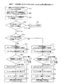
(B)パケットプロセッサとCAM間の送受信処理
図3は回線カードが連想データ(ルーチングデータ)を取得するための、パケットプロセッサとCAM間の送受信処理フロー、図4はパケットプロセッサとCAM間の送受信データのデータフォーマット、図5はパケットプロセッサとCAM間の送受信データタイムチャートである。
回線カード13のパケットプロセッサ13aは回線から受信したIPパケットのIPヘッダより宛先アドレスDAを検索し、該宛先アドレスDAを検索キーデータ51(図4(A)参照)として抽出する(ステップ201)。ついで、パケットプロセッサ13aは、スイッチ12が検索キーデータであると認識できるようにするために該検索キーデータ51にキーフラグ52を付加すると共に、主制御部が回線速度を識別できるようにIPパケットが到来した回線の識別子(Line ID)53を付与し(ステップ202)、検索キーデータをスイッチ12に入力する(ステップ203)。
【0027】
スイッチ12は受信した転送データの先頭ビット(フラグ)を参照し(ステップ204)、先頭ビットがデータフラグであれば転送データはパケットであると判定し、ルーチングデータに基づいてパケットを所定の回線カードにスイッチングする(ステップ205)。
受信した転送データの先頭ビットがキーフラグであれば、スイッチ12は0系、1系の主制御部11,11′のいずれが運用中であるか判断し(ステップ206)、運用中の主制御部にフラグを削除して回線識別子53と検索キーデータ51を送出する。例えば、0系の主制御部11が運用中であるとすれば、スイッチ12はフラグを削除して(回線識別子+検索キーデータ)を主制御部11のバスブリッジ11fに送出する。尚、スイッチが二重化されている場合には、スイッチ12は転送元スイッチを特定するスイッチ識別子SW ID54をキーデータに付加する。
バスブリッジ11fは、受信データに送り先(クロスコネクト部)のバスアドレス55を付与してシステムバス11gを介してクロスコネクト部11dへ転送する(ステップ207)。
【0028】
クロスコネクト部11dは受信データより検索キーデータ51、回線識別子53を分離し(ステップ208)、回線識別子53から使用するCAMをデコードし、該当CAMが存在するか判別する(ステップ209)。すなわち、回線識別子53に基づいて回線速度を求め、該回線速度に応じたCAMを求め、該CAMが主制御部11に実装されているかチェックする。該当CAMが主制御部11に実装されていなければエラー処理し(ステップ210)、実装されていれば該当CAMをアクセス可能にイネーブルする(ステップ211)。ついで、クロスコネクト部11dは検索キーデータ51を該当CAM 11eに転送する(ステップ212)。該当CAM 11eは検索キーデータ51に基づいて連想データ(ルーチングデータ)56を検索し(ステップ213)、該連想データ(Associate Data)をクロスコネクト部11dに返す。
【0029】
クロックコネクタ部11dは、連想データ56に元の回線識別子53、スイッチ識別子54を付加すると共に送り先(バスブリッジ11f)のバスアドレス57を付与してシステムバス11gに送出する。バスブリッジ11fはクロスコネクト部11dから受信したデータよりバスアドレス56、スイッチ識別子54を削除し、スイッチ識別子が示すスイッチ12に(回線識別子53+連想データ56)を入力する。スイッチ12は回線識別子53を削除し、連想データ56を所定回線カードのパケットプロセッサ13aに入力する(ステップ214)。
以上はステップ206において、0系の主制御部11が運用中であるとした場合である。しかし、1系の主制御部11′が運用中であるとすれば、1系主制御部11′はステップ217〜224において0系主制御部11のステップ207〜214と同様の処理を実行する。
【0030】
(b) 通常パケットのスイッチング
パケットプロセッサ13aは連想データを受信すれば、ルーチングデータ(ハイウェイ番号HW No.)、その他の情報αを取り出し、これら情報(HW No.+α)61をIPパケット(ペイロード)62に付加してスイッチ12に入力する(図4(B)参照)。尚、先頭の1bitに一連の転送データがスイッチングすべき通常パケットであることを示すデータフラグ(Data Flag)63を付与する(以上、ステップ202,203)。
スイッチ12は受信した転送データの先頭ビット(フラグ)を参照し(ステップ204)、先頭ビットがデータフラグであれば転送データはパケットであると判定し、フラグを除去し、ルーチングデータ61に基づいてパケットを所定の回線カードにスイッチングする(ステップ205)。該回線カードはスイッチ12よりパケットを受信すれば、ルーチングデータを削除し、SONET/SDHのペイロードにマッピングして回線へ送出する。
【0031】
図5のタイムチャートは横軸に時間をとったものである。本発明のルーチング装置は、スイッチ12、システムバス11gを経由するインバンド方式によりCAMへアクセスする。このため、ルーチングデータを得るのに多少の時間を必要とする。しかし、システムバスの速度向上、スイッチの動作速度向上により、実際のアクセス時間を短くすることができ、従来型ルーチング装置のアクセス時間と遜色なく動作可能である。
【0032】
(C)回線カードの異種回線の混在搭載
図1では各回線カード131〜13nは同一構成であることを想定して説明したが、回線カードは複数のパケットプロセッサを備えていてもよく、又、収容する回線の速度は任意でよい。図6は異種回線の混在搭載を説明する説明図であり、回線カード131には1つのパケットプロセッサ13aと1つのMPU 13bが搭載され、4種類の速度の異なる回線OC-3, OC-12, OC-48, OC-192が収容されている。回線カード132には、2つのパケットプロセッサ13a1,13a2と1つのMPU 13bが搭載され、4種類の速度の異なる回線OC-3, OC-12, 100BT、Gi-etherが収容されている。回線カード13nには、4つの同一回線OC-12が搭載されている。
【0033】
本発明のルーチング装置は、主制御部11に各回線速度に対応させてCAM11e1〜11enをそれぞれ備える。主制御部11は回線カード131〜13nから回線識別子が付加された検索キーデータを受信すれば、回線速度に応じたCAMからルーチングデータを求めて要求元の回線カードに送出する。この結果、速度の異なるCAMを回線速度毎に使い分けることが可能となり、しかも、図6に示すように回線カード131〜13nに種々の速度の回線を収容することが可能となる。すなわち、本発明の類装置は、安価で低速のCAMを使用でき、しかも、回線カードの回線収容効率を向上でき、コストダウンを図ることができる。
【0034】
(D)CAM周辺の構成
図7はCAM周辺の回路構成図であり、図1と同一部分には同一符号を付している。クロスコネクト部11d内のバスコントローラ31は、システムバス11gと連想データバス(Associate Data Bus)32、キーデータバス(Key Data Bus)23間のバス調停制御を行う。連想データバス32は、クロスコネクト部内に設けられ、CAM 11e1〜11enを構成する連想メモリ21(図1参照)から読出された連想データ等を伝送する。キーデータバス33は、クロスコネクト部内に設けられ、CAMを構成するキーデータ記憶部22や連想メモリ21に書き込むキーデータ/連想データやルーチングデータ検索用のキーデータ(検索キーデータ)等を伝送する。すなわち、バスコントローラ31は、メインプロセッサ11aからシステムバス11gを介して入力するルーチングテーブル(キーデータ/連想データ)をキーデータバス33に送出し、所定のCAMに書き込む。又、ルーチングデータ検索時に、回線カードからシステムバス11gを介して入力する検索キーデータをキーデータバス33に送出する。又、CAMから読出された連想データ等を連想データバス32を介してシステムバス11gに送出する。
【0035】
CAMセレクタ34は、回線カード131〜13nからインバンド方式で受信するデータより、▲1▼キーデータ51、▲2▼回線識別子(Line ID)53、▲3▼スイッチ識別子(SW ID)の分離を行い、キーデータをCAMへ送出すると共に回線識別子、スイッチ識別子を保持し、後述のラインセレクタ35に入力する。又、CAMセレクタ34は、回線識別子53からアクセスすべきCAMを選択し、そのCAMに対し制御線を介してアクセスイネーブル信号ACENを送出する。図8はルーチングデータ検索時におけるCAMアクセスのタイムチャートである。CAMセレクタ34は、クロックに同期してアクセスイネーブル信号ACENをハイレベルにし、しかる後、キーデータKDTをクロックに同期してCAMに送出する。
ラインセレクタ35は、CAMより検索した連想データ(Associate Data)にCAMセレクタ34から入力する回線識別子53、スイッチ識別子54を付与して連想データバス32に送出する。
【0036】
バスコントローラ36は、クロスコネクトバス14と連想データバス32、キーデータバス23間のバス調停制御を行う。運用系の主制御部11のメインプロセッサ11aは、内部のCAM 11e1〜11enのルーチングテーブルを更新するとき、あるいは、これらCAM 11e1〜11enに新たにルーチングテーブルを書き込むとき、スタンバイ系の主制御部11′内のCAM 11e1′〜11en′にもルーチングテーブルの更新、書き込みを行なう。かかる場合、バスコントローラ36はバス調停制御を行ってメインプロセッサ11aからのルーチングテーブルをクロスコネクトバス14を介してスタンバイ系主制御部11′に送出する。
【0037】
(E)CAMの内部構成
図9はCAMの内部構成図であり、図1と同一部分には同一符号を付している。I/O制御部20はキーデータと連想データの入出力制御を行うもので、クロスコネクト部側から各種データ(キーデータ/連想データ/検索キーデータ)、制御信号、イネーブル信号が入力し、又、クロスコネクト部側へ連想データ/マルチプルヒット関連データ等を出力する。
連想メモリ部21は連想データ(ルーチングデータHW-No.+α)を記憶し、キーデータ記憶部22は宛先アドレスをキーデータとするとき、多数の宛先アドレスに応じたキーデータを記憶する。連想メモリ21とキーデータ記憶部22は1つメモリアレイの連続領域で構成され、プログラマブルに連想データのビット幅rやキーデータのビット幅k、領域境界線を可変に設定できるようになっている。
【0038】
アドレス変換部23は各回線カードから要求された宛先アドレスDAに応じたキーデータ(検索キーデータ)がキーデータ記憶部22に存在するとき、キーデータを連想メモリ21のアドレスに変換するもので、レスポンスレジスタ23a、プライオリティエンコーダ23bを備えている。レスポンスレジスタ23aは、 (1) キーデータ記憶部22に記憶されている円とキーデータと検索キーデータとのマッチング結果(比較結果)、あるいは、(2) キーデータ記憶部22に記憶されているエントリキーデータと検索キーデータの非マスク部分とのマッチング結果を格納する。プライオリティエンコーダ23bはレスポンスレジスタ23aのマッチング結果をもとに連想メモリ21のアドレスを生成し、連想メモリ21の該アドレスより連想データ(ルーチングデータHW-No.+α)を出力する。キーデータ記憶部22に記憶されている複数のキーデータが検索キーデータと一致する場合(マルチプルヒット)、プライオリティエンコーダ23bは予め定められている基準に基づいて定まる1つのエントリキーデータに応じたアドレスを発生する。このアドレスから読出した連想データによりパケットを送ってみて、パケットが宛先に届かなければ要求により次のエントリキーデータに応じたアドレスを出力し、以後同様にシーケンシャルにアドレスを出力する。
【0039】
メモリアクセス部24は、メモリアレイへのキーデータ/連想データの書き込み制御、検索キーデータに応じた連想データの読出し制御をするもので、アドレスデコーダ24a、インデックス/マスクレジスタ24b、モード設定レジスタ24cを備えている。アドレスデコーダ24aは入力するアドレスデータをデコードしてメモリアレイの所定のアドレスにキーデータ/連想データを書き込み(ルーチングテーブル更新時)、あるいはメモリアレイの所定ドレスよりキーデータ/連想データを読み出す(ルーチングデータ検索時)。インデックス/マスクレジスタ24bは検索キーデータおよびマスクデータを記憶する。モード設定レジスタ24cはキーデータのビット幅k/連想データのビット幅r/エントリ数eを保持するもので、エントリ数eはメモリアレイに保存可能なキーデータ数(=連想データ数)である。アドレスデコーダ24aはk,r,eに基づいてアドレスデータに応じたキーデータ領域22および連想データ領域21におけるアドレスを発生してキーデータおよび連想データの読み/書き制御を行なう。このように、従来、CAM LSI外部に配置していたRAM構成の連想メモリをCAM LSI内部に配置することによりメモリアレイを有効に活用することが可能になり、又、キーデータ幅や連想データ幅が変更になってもモード設定レジスタ24cの設定データのみの変更により対応することができる。
【0040】
マルチプルヒット管理部25は、キーデータ記憶部22に記憶されている複数のキーデータが検索キーデータと一致する時(マルチプルヒット時)、ヒット数CHをヒットレジスタ25aに格納すると共に、検索キーデータとマッチングするエントリキーデータをキーデータレジスタ25に格納し、適宜、ヒット数CHおよびエントリキーデータの組をI/Oコントローラ20を介してメインプロセッサ11aに送出する。以上のように、マルチプルヒット管理部25がヒット数およびエントリキーデータを管理するため、メインプロセッサ11aは必要に応じてこれら管理データを読みとって所定の処理を行なうだけでよいため、マルチプルヒット時におけるメインプロセッサの処理を軽減することができる。尚、メインプロセッサの処理としては、キーデータ記憶部22に記憶されているキーデータの誤り検出処理等がある。
【0041】
(F)メモリアレイおよび周辺回路
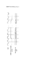
図10はメモリアレイお及びその周辺回路の構成図であり、図9と同一部分には同一符号を付している。RAM構成のメモリアレイMCAの前半はキーデータ記憶領域22、後半が連想メモリ領域21になっている。メモリアレイMCAの1バイトセルの総数をy、キーデータ幅をkバイト、ルーチングデータを含む連想データ幅をrバイトとするとき、メモリアレイに登録可能なキーデータおよび連想データの数(エントリ数)eは、キーデータ数と連想データ数が同じであるから次式
e=y/(k+r) (1)
により求まり、これらk,r,eはモード設定レジスタ24cに設定される。エントリ数eは例えばI/Oコントローラ20(図9)が演算してモード設定レジスタ24cに設定する。図11はメモリアレイにおける1バイトセル数y、キーデータ幅k、連想データ幅r、エントリ数eの関係図表であり、エントリ数は(1)式により求まる。図11の図表において、左欄はメモリアレイのセルバイト数が1000、右欄はセルバイト数が16,384の場合におけるy,k,r,eの関係を示している。
【0042】
キーデータ記憶領域22の第iキーデータアドレスに対応するセルバイトアドレスはこれらk,r,eより、以下
i・k〜i・k+(k-1) (2)
で与えられる。又、連想メモリ領域21の第j連想データアドレスに対応するセルバイトアドレスは以下
k・e+j・r〜k・e+j・r+(r-1) (3)
で与えられる。アドレスデコーダ24aはモード設定部24cに設定されたk,r,eを参照し、(2),(3)式により入力するアドレスデータをメモリアレイMCAのバイトアドレスに変換する。
【0043】
・キーデータの書き込み
メモリアレイMCAに対すキーデータ書き込みに際して、キーデータがメモリアレイMCAに入力し、キーデータの書き込みアドレスiがアドレスデコーダ24aに入力すると、アドレスデコーダ24aはアドレスデータiを(2)式に従ってデコードし、デコードにより求まるバイトアドレスが示すk個の1バイトセルにキーデータを書き込む。以後、同様に順次キーデータをメモリアレイMCAのキーデータ記憶領域22に書き込む。
・連想データの書き込み
メモリアレイMCAに対する連想データの書き込みに際して、連想データがメモリアレイMCAに入力し、連想データの書き込みアドレスjがアドレスデコーダ24aに入力すると、アドレスデコーダ24aはアドレスデータjを(3)式に従ってデコードし、デコードにより求まるバイトアドレスが示すr個の1バイトセルに連想データを書き込む。以後、同様に順次連想データをメモリアレイMCAの連想メモリ領域21に書き込む。
【0044】
・検索キーデータに応じた連想データの読出し
検索キーデータに応じた連想データを出力するには、該検索キーデータをインデックス/マスクレジスタ24bに入力して記憶すると共に、アドレスデコーダ24aにキーデータの読出しアドレスi=1〜eを順次入力する。アドレスデコーダ24aはアドレスデータiを(2)式に従ってデコードし、デコードされたバイトアドレスが示すk個のバイトセルからkバイトのキーデータ(エントリキーデータ)を読み出し、ゲート26を介してインデックス/マスクレジスタ24bに入力する。インデックス/マスクレジスタ24bはその比較機能により、検索キーデータとエントリキーデータを比較し、比較結果をレスポンスレジスタ23aに格納する。以後、同様に、アドレスデータiを歩進し、i=1〜eが示すキーデータアドレスから読み取ったエントリキーデータと検索キーデータとの比較結果をレスポンスレジスタ23aに格納する。比較処理が終了すれば、プライオリティエンコーダ23bは検索キーデータと一致したエントリキーデータを連想メモリ領域21のアドレスjに変換し、アドレスデコーダ24aに入力する。アドレスデコーダ24aは入力する連想データアドレスjを(3)式に従ってデコードし、デコードにより得られたバイトアドレスの示すr個のバイトセルからrバイトの連想データを読出し、ゲート26を介して出力する。
以上のように、本発明のルーチング装置によれば、連想データやキーデータのビット幅を変更する際、変更後の連想データのビット幅rやキーデータのビット幅kを入力するだけでよく、CAM周辺回路の設計変更をする必要がない。
【0045】
(G)各ユニット間のデータの流れ
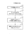
(a)CAM-メインプロセッサ間のデータの流れ
図12はCAM−メインプロセッサ間のデータの流れを説明する説明図である。運用系の主制御部11のメインプロセッサ11aは、内部のCAM 11e1〜11enにアクセスするとき、ルートR1を介して行なう。従って、メインプロセッサ11aがルーチングテーブル(キーデータ/連想データ)を内部のCAM11e1〜11enに書き込む際、該ルートR1を介して行なう。又、内部CAMより連想データ等を読み出すときにも該ルートR1を介して行なう。 又、運用系の主制御部11のメインプロセッサ11aは、スタンバイ系主制御部11′の内部のCAM 11e1′〜11en′にアクセスするとき、図8のルートR2を介して行なう。従って、メインプロセッサ11aがルーチングテーブルを二重化するためにCAM 11e1′〜11en′に該ルーチングテーブルを書き込む際、ルートR2を介して行なう。
【0046】
(b)CAM−パケットプロセッサ間のデータの流れ
図13はCAM−パケットプロセッサ間のデータの流れを説明する説明図である。運用系のCAMと回線カードのパケットプロセッサ間のデータ送受はルートR1〜R3を介して行なわれる。ルートR1は回線カード131が検索キーデータを運用系のCAM 11e1へ与えて検索結果(ルーチングデータ)を受信する場合のルートである。ルートR2は回線カード132が検索キーデータを運用系のCAM 11enへ与えて検索結果(ルーチングデータ)を受信する場合のルートである。ルートR3は主制御部11′が運用系になった場合、回線カード13nが検索キーデータを運用系のCAM 11e1′へ与えて検索結果(ルーチングデータ)を受信する場合のルートである。
【0047】
(c)障害時のCAM−パケットプロセッサ間のデータの流れ
図14は障害時のCAM−パケットプロセッサ間のデータの流れを説明する説明図である。障害発生前は、回線カード131のパケットプロセッサ13aはルートR1を介して運用系主制御部11のCAM 11e1〜11enにアクセスしてルーチングデータを取得する。しかし、CAM 11e1〜11enに障害が発生して主制御部11′が運用系になれば、パケットプロセッサ13aはルートR2を介して運用系の主制御部11′のCAM 11e1′〜11en′にアクセスしてルーチングデータを取得する。
【0048】
・付記
(付記1) 回線より到来するパケットの宛先アドレスに応じたルーチングデータを求めてパケットに付加し、該ルーチングデータに基づいてパケットをスイッチングして所定の回線に送出するルーチング装置において、
ルーチングデータ発生部を備え、要求された宛先アドレスに応じたルーチングデータを発生して要求元に送出する主制御部、
回線より到来するパケットの宛先アドレスを抽出し、該宛先アドレスに応じたルーチングデータを通知するよう主制御部に要求し、主制御部より通知されたルーチングデータをパケットに付加して出力する回線インタフェース部、
所定の回線インタフェース部から入力する前記ルーチングデータ要求を主制御部に送出し、主制御部からのルーチングデータを要求元の回線インタフェース部に送出し、ルーチングデータ付きパケットを該ルーチングデータに基づいてスイッチングして別の回線インタフェース部に送出するスイッチ部、
を備えたことを特徴とするルーチング装置。
【0049】
(付記2) 前記主制御部のルーチングデータ発生部は、
ルーチングデータを記憶する連想メモリ部、
宛先アドレスをキーデータとするとき、多数の宛先アドレスに応じたキーデータを記憶するキーデータ記憶部、
前記要求された宛先アドレスに応じたキーデータがキーデータ記憶部に存在するとき、該キーデータを前記連想メモリのアドレスに変換する変換部、
連想メモリ部の該アドレスよりルーチングデータを読出して要求元である回線インタフェース部に送出するルーチングデータ送出部、
を備えたことを特徴とする付記1記載のルーチング装置。
(付記3) 前記主制御部を二重化し、運用中の主制御部は前記各記憶部の記憶内容を更新するとき、スタンバイ中の主制御部の各記憶部の記憶内容も更新し、運用中の主制御部側に障害が発生したとき、スタンバイ中の制御部は新たに運用中制御部としてルーチング制御を継続する、
ことを特徴とする付記2記載ルーチング装置。
【0050】
(付記4)前記主制御部は、回線速度に対応させてルーチングデータ発生部を備え、
前記回線インタフェース部は、回線より到来するパケットの宛先アドレスに応じたキーデータに回線識別子を付加して主制御部にルーチングデータを通知するよう要求し、
主制御部は、該通知要求により回線識別子の回線速度に応じたルーチングデータ発生部よりルーチングデータを発生して要求元の回線インタフェース部に送出する、
ことを特徴とする付記2記載のルーチング装置。
【0051】
(付記5) 回線インタフェース部に任意の回線速度の回線を接続する、
ことを特徴とする付記4記載のルーチング装置。
(付記6) 各回線インタフェース部は、主制御部へ送出するルーチングデータ要求にキーフラグを付し、パケットにデータフラグを付してスイッチ部に入力し、
スイッチ部はキーフラグ付きデータを主制御部に送出し、データフラグ付きパケットをルーチングデータに基づいて出力側の回線インタフェース部に送出する、
ことを特徴とする付記2記載のルーチング装置。
【0052】
(付記7) 前記連想メモリ部とキーデータ記憶部を1つメモリアレイの連続領域で構成し、
メモリアレイの1バイトセルの総数をy、キーデータ幅をkバイト、ルーチングデータを含む連想データ幅をrバイトとするとき、登録可能なキーデータ数および連想データ数であるエントリ数eを
e=y/(k+r)
により演算し、これらk,r,eによりキーデータおよび連想データのキーデータ領域および連想データ領域への読み/書き制御を行なう、
ことを特徴とする付記2記載のルーチング装置。
(付記8) 前記ルーチングデータ発生部は、
前記キーデータ幅k、連想データ幅r、エントリ数eを保持するレジスタ、
k,r,eによりキーデータおよび連想データの読み/書き制御を行なうアドレスデコーダ、
を備えたことを特徴とする付記7記載のルーチング装置。
【0053】
(付記9) 前記主制御部のルーチングデータ発生部は、更に、
前記要求された宛先アドレスに応じたキーデータと同一のキーデータ、あるいは、該宛先アドレスに応じたキーデータの非マスク部分と同一のキーデータがキーデータ記憶部に複数エントリされているとき、そのエントリ数、エントリキーデータを保持する保持部、
これらエントリ数、エントリキーデータを外部のプロセッサに通知する手段、
を備えたことを特徴とする付記2記載のルーチング装置。
以上、本発明を実施例により説明したが、本発明は請求の範囲に記載した本発明の主旨に従い種々の変形が可能であり、本発明はこれらを排除するものではない。
【0054】
【発明の効果】
以上本発明によれば、従来、個々の回線カードと主制御部の両方に配置していたCAM(ルーチングデータ発生部)を主制御部側に集約してルーチングテーブルを一元管理するように構成したから、システム全体で使用しているCAMの個数を削減でき、コストダウンと実装効率を向上することができる。
又、本発明によれば、CAMを主制御部にのみ持たせるだけでよいため、システム立ち上げの際、主制御部のメインプロセッサから回線カードにルーチングテーブルを転送する必要がなく、電源投入時やリカバリー時におけるシステム立ち上げ時間を減少することができる。
【0055】
又、本発明によれば、主制御部は、回線インタフェース部から回線識別子付きのルーチングデータ要求があったとき、回線速度に応じたCAMからルーチングデータを求めて要求元の回線インタフェース部に送出するように構成したから、速度の異なるCAMを回線速度毎に使い分けることが可能となり、安価で低速のCAMを使用でき、しかも、回線カードに種々の速度の回線を収容することが可能となり、回線カードの回線収容効率を向上できる。この結果、ルーチング装置のコストダウンを図ることができる。
又、本発明によれば、主制御部を二重化し、運用中の主制御部はCAMの記憶内容(ルーチングテーブル)を更新するとき、スタンバイ中の主制御部の各CAMのルーチングテーブルも更新し、運用中の主制御部側に障害が発生したとき、スタンバイ中の制御部は新たに運用中制御部としてルーチング制御を継続するように構成したから、CAMをメインプロセッサへ集約した場合の障害発生時の信頼性を向上させることができる。
【0056】
又、本発明によれば、連想メモリ部とキーデータ記憶部を1つのメモリアレイで構成し、該メモリアレイの連続する2つの領域をそれぞれ連想メモリ部、キーデータ記憶部とし、メモリアクセス部はメモリアレイの1バイトセルの総数y、キーデータ幅k、連想データ幅rより自動的にメモリアレイに登録可能なキーデータおよび連想データの数(エントリ数)eを求め、これらy,k,r,eに基づいてキーデータおよび連想データのメモリアレイへの読み/書き制御を行なう。このようにすれば、CAM周辺回路の設計変更をしなくてもy,k,rをプログラマブルに変更するだけで連想データやキーデータのビット幅を可変制御することができる。
又、本発明によれば、主制御部のルーチングデータ発生部にマルチプルヒットしたエントリ数(ヒット数)、エントリキーデータの管理を行なわせるようにしたから、マルチプルヒット時の処理をCAM LSI内部にて実現でき、メインプロセッサの処理を少なくして負荷を軽減することができる。
【図面の簡単な説明】
【図1】本発明におけるシステム構成図である。
【図2】CAM検索最低時間を示す図表である。
【図3】連想データを取得するためのCAM−パケットプロセッサ間の動作処理フローである。
【図4】CAMーパケットプロセッサ間の送受信データフォーマットである。
【図5】CAMーパケットプロセッサ間の送受信タイムチャートである。
【図6】回線カードにおける複数異種回線の混在搭載説明図である。
【図7】CAM周辺の構成図である。
【図8】CAMアクセスのタイムチャートである。
【図9】CAMの内部構成図である。
【図10】メモリアレイと周辺回路の構成図である。
【図11】RAMセル幅、キーデータ幅、連想データ幅、エントリ数の関係図表である。
【図12】CAM−メインプロセッサMPU間のデータの流れ説明図である。
【図13】CAM−パケットプロセッサ間のデータの流れ説明図である。
【図14】障害時のCAM−パケットプロセッサ間のデータの流れ説明図である。
【図15】従来のルータの概略構成図である。
【図16】回線カードの構成図である。
【図17】CAM検索の流れ図である。
【図18】従来のルータ装置の詳細な構成図である。
【図19】従来のルータ装置のパケットの流れ説明図である。
【図20】 CAM LSIの内部構造説明図である。
【符号の説明】
11、11′・・主制御部
11e1〜11en・・CAM
12・・スイッチ部
131〜13n・・回線カード
13a・・パケットプロセッサ[0001]
BACKGROUND OF THE INVENTION
The present invention relates to a routing apparatus that uses a CAM (Content Addressable Memory) for routing processing in the Internet, ATM network, etc., and in particular, routing data corresponding to the destination address of a packet coming from a line is obtained from the CAM and added to the packet. The present invention relates to a routing device that switches packets based on the routing data and sends the packets to a predetermined line.
[0002]
[Prior art]
With the recent explosive spread of the Internet / ATM network, the processing speed of routers / ATM switches (ATM switches) is steadily increasing. In addition, as the circuit is highly integrated, a table for retrieving data (routing data) necessary for the routing / switching is also increasing in capacity.
The routing data search method is achieved by a conversion processing technique using CAM (Content Addressable Memory). However, as the capacity of the CAM increases, a large number of tables are required for the conventional capacity, and it is difficult to mount the CAM inside a normal LSI. Large-capacity devices are also marketed as dedicated LSIs.
[0003]
FIG. 15 is a schematic configuration diagram of a conventional router, which explains an outline of a search method using a CAM in a general router. 1 is the main control unit (CPU), 2 is the switch unit, 3 1 ~ 3n, 4 1 -4m is a line card provided between the line and the switch. Data transmission on the line is generally transmission using POS (Packet over SONET, Packet over SDH). In this POS, IP packets are mapped to SDH and SONET payload parts and transmitted. A line termination unit (not shown) separates the IP packet from the POS line, and the
[0004]
FIG. 16 shows that
[0005]
FIG. 18 is a detailed block diagram of a conventional router. The same parts as those in FIGS. The
[0006]
Line card 3 1 -3n accommodates various lines such as SONET / SDH and has the same configuration. However, the speed of each line accommodated by the line card is the same, but the line speed is different for each line card. The
The
[0007]
FIG. 19 is an explanatory diagram showing a packet flow of a conventional router device.
1) Data packets input from the POS line are separated into packets at the input part in the
2) The
3) The
4) Next, the
[0008]
FIG. 20 is a schematic internal structure diagram of the CAM LSI.
The
[0009]
In FIG. 20, the key data is shown as 8 bits, but for convenience of explanation, the key data is actually 32 bits. Although the
[0010]
[Problems to be solved by the invention]
A conventional routing device (router) using a CAM has the following problems.
1) High cost of CAM LSI
With the recent spread of the Internet, the number of CAM entries continues to increase. The number of entries that can be processed per CAM LSI is at most about 64k if 36 bits are required per entry. Here, 36 bits is a total of 32 bits necessary as a destination address in IP_v4 (IP-version 4) and 4 bits as a control bit.
[0011]
2) High mounting surface area ratio of CAM LSI
As described above, if it is necessary to mount 15 CAM LSIs (about 4 × 4 cm), the mounting surface occupation ratio becomes high. For this reason, the circuit card has to have a complicated structure such as a two-story structure.
3) Routing table transfer time
It is necessary to transfer the routing table from the main processor of the main control unit that centrally manages the routing table to each line card. For example, when starting up the system, it is necessary to transfer the routing table from the main processor of the main control unit to the CAM installed in each line card. For this reason, it takes a considerable amount of time to start up the system, and it also takes time to recover when a failure occurs.
[0012]
4) Changing the bit width of associative data
The CAM has a configuration in which an associative memory having a RAM configuration is externally attached to the CAM LSI. For this reason, when the key data is changed from IP_v4 to IP_v6 (4 bytes → 16 bytes), etc., it becomes necessary to change the hardware circuit configuration, and a new line card must be redesigned.
5) Multiple hit of key data
Since the conventional CAM does not have a statistical processing function, statistical processing cannot be executed at the time of multiple hit (Multiple hit) in which a plurality of entry key data hits the search key data. For this reason, it is necessary for the main processor MPU of the main control unit to calculate statistical information by program processing on the main memory MM. This statistical processing places a heavy load on the main processor.
[0013]
6) Relationship between line speed and CAM
A conventional router mounts a CAM on a line card, and accommodates a plurality of lines of the same speed (for example, OC-12 lines × 4) on the line card. The reason for this is that a configuration in which lines having different speeds are accommodated in the line cards requires expensive CAMs with the highest speed for all line cards, resulting in an increase in cost. However, in a router with a conventional configuration that accommodates the same speed line for each line card, it is necessary to prepare a line card corresponding to each line speed. Depending on the network, a line card that is not used may be generated or accommodated in the line card. There are cases where the number of connected lines is small. In other words, the conventional routing device has poor line accommodation efficiency of the line card, which increases the cost.
[0014]
Accordingly, an object of the present invention is to provide an inexpensive and compact routing device.
Another object of the present invention is to reduce the number of CAMs used and increase the cost and mounting efficiency of the routing device.
Another object of the present invention is to improve the reliability of the routing device by allowing the operation to continue even if a failure occurs.
Another object of the present invention is to provide a routing device that can variably control the bit width of associative data and key data in the CAM without changing the design of circuits around the CAM.
Another object of the present invention is to reduce the main processor statistical processing and reduce the load on the main processor by enabling processing at the time of multiple hits to be realized inside the CAM LSI.
Another object of the present invention is to reduce the cost of the routing device by making it possible to use different CAMs for different line speeds and to accommodate lines of various line speeds in the line card. .
Another object of the present invention is to provide a routing device that can reduce the system start-up time when power is turned on or during recovery.
[0015]
[Means for Solving the Problems]
The present invention is a routing device that obtains routing data according to a destination address of a packet coming from a line, adds the routing data to the packet, switches the packet based on the routing data, and sends the packet to a predetermined line. A main control unit that includes a routing data generation unit, generates routing data corresponding to the requested destination address, and sends it to the request source; (2) extracts the destination address of the packet arriving from the line, and according to the destination address A line interface unit that requests the main control unit to notify the routing data, and adds the routing data notified from the main control unit to the packet and outputs the packet; (3) the routing data request input from a predetermined line interface unit Is sent to the main control unit, and the routing data from the main control unit is sent to the requesting line interface unit. And, a switch unit, to be transmitted to another line interface unit by switching on the basis of the routing data packet with the said routing data.
[0016]
The routing data generation unit of the main control unit consists of (1) an associative memory unit for storing routing data, and (2) a large number of destination addresses when the destination address is used as key data. Is A key data storage unit for storing key data; (3) the requested destination address; Is A conversion unit that converts the key data into an address of the associative memory when the key data exists in the key data storage unit; (4) reads out the routing data from the address of the associative memory unit and sends it to the requesting line interface unit; A routing data transmission unit for transmission;
The routing device of the present invention centrally manages the routing table by consolidating CAM (routing data generation unit), which has been conventionally arranged in both the individual line cards and the main control unit, on the main control unit side. As a result, the number of CAMs used in the entire system can be reduced, and cost reduction and mounting efficiency can be improved.
Also, since it is only necessary to have the CAM only in the main control unit, there is no need to transfer the routing table from the main processor of the main control unit to the line card at the time of system startup, and the standing system at the time of power-on or recovery Can increase the raising time
[0017]
The routing device according to the present invention includes a routing data generator (CAM) corresponding to each line speed in the main controller. When there is a routing data request with a line identifier from the line interface unit, the main control unit obtains the routing data from the CAM corresponding to the line speed and sends it to the requesting line interface unit. In this way, CAMs with different speeds can be used for each line speed, and various line speeds can be accommodated in the line card, and an inexpensive and low-speed CAM can be used. Since the line accommodation efficiency of the card can be improved, the cost of the routing device can be reduced.
[0018]
In the routing device of the present invention, the associative memory unit and the key data storage unit are constituted by one memory array, and two consecutive areas of the memory array are used as the associative memory unit and the key data storage unit, respectively. When the total number of 1-byte cells in the memory array is y, the key data width is k bytes, and the associative data width including routing data is r bytes, the access unit for the memory array has the number of key data and associative data that can be registered. The number of entries e is given by
e = y / (k + r)
The key data and associative data are read / written to the memory array using k, r, and e. In this way, the bit width of associative data and key data can be variably controlled by simply changing y, k, and r without changing the design of the circuits around the CAM.
In the routing device of the present invention, the routing data generation unit of the main control unit manages the number of entries having multiple hits and the entry key data. In this way, the processing at the time of multiple hits can be realized inside the CAM LSI, and the statistical processing of the main processor can be reduced to reduce the load.
[0019]
DETAILED DESCRIPTION OF THE INVENTION
(A) System configuration
FIG. 1 is a system configuration diagram of a routing apparatus according to the present invention.
The
[0020]
CAM11e 1 ~ 11en, 11e 1 ′ To 11en ′ are (1) an
[0021]
The
[0022]
The routing device of FIG. 1 has the following features.
1) CAM mounting position
Conventionally, each CAM that has been arranged on both the individual line card and the main control unit is aggregated on the
[0023]
2) CAM LSI duplex configuration
In order to improve the reliability when a failure occurs when the CAM is integrated into the
[0024]
3) Introduction of CAM for line speed
The CAM becomes more expensive as the latency is lower, in other words, as the access time is shorter. For this reason, a configuration using only a single type of CAM capable of high-speed increases the cost. The routing device of the present invention has a plurality of
[0025]
Usually, the minimum time required for the CAM search for each line is the packet transmission time. That is, it is necessary to finish the CAM search during transmission of one packet, and the time becomes stricter as the line speed increases and the number of transfer data decreases. 2A and 2B are tables showing examples of the minimum CAM search time of the POS line. FIG. 2A shows the case of OC-12C, and FIG. 2B shows the case of OC-192C.
Since the transfer time per bit of OC-12C is 1.6ns, the total transfer time is
1.6 x (IP data fluctuation n + PPP + IP header fixed part)
If the IP data fluctuation is 1 to 1500 bytes, the transfer time is 0.36 ns to 19.64 ns. On the other hand, in the case of OC-192C, the transfer time per bit is 0.1 ns, so the total transfer time is
0.1 x (IP data fluctuation n + PPP + IP header fixed part)
If the IP data fluctuation is 1 to 1500 bytes, the transfer time is 0.02 ns to 1.23 ns. Since it is necessary to finish the CAM search during transmission of one packet, an expensive high-speed accessible CAM is used if the line speed is high, and an inexpensive low-speed CAM is used if the line speed is low.
[0026]
(B) Transmission / reception processing between the packet processor and the CAM
3 shows a transmission / reception processing flow between the packet processor and the CAM for the line card to acquire associative data (routing data), FIG. 4 shows a data format of transmission / reception data between the packet processor and the CAM, and FIG. It is a transmission / reception data time chart between.
The
[0027]
The
If the first bit of the received transfer data is a key flag, the
The
[0028]
The
[0029]
The
The above is a case where it is assumed in
[0030]
(b) Normal packet switching
When the
The
[0031]
The time chart of FIG. 5 is time taken on the horizontal axis. The routing device of the present invention accesses the CAM by an in-band method via the
[0032]
(C) Mixed installation of different types of line cards
In FIG. 1, each
[0033]
The routing device of the present invention causes the
[0034]
(D) Configuration around CAM
FIG. 7 is a circuit configuration diagram around the CAM, and the same parts as those in FIG. The
[0035]
The
The
[0036]
The
[0037]
(E) Internal structure of CAM
FIG. 9 is a diagram showing the internal structure of the CAM. The same parts as those in FIG. The I /
The
[0038]
The
[0039]
The
[0040]
The multiple
[0041]
(F) Memory array and peripheral circuit
FIG. 10 is a block diagram of the memory array and its peripheral circuits. The same parts as those in FIG. The first half of the RAM-structured memory array MCA is a key
e = y / (k + r) (1)
These k, r, and e are set in the
[0042]
The cell byte address corresponding to the i-th key data address of the key
i ・ k〜i ・ k + (k-1) (2)
Given in. The cell byte address corresponding to the jth associative data address in the
k ・ e + j ・ r〜k ・ e + j ・ r + (r-1) (3)
Given in. The
[0043]
・ Write key data
When writing key data to the memory array MCA, when the key data is input to the memory array MCA and the key data write address i is input to the
・ Associative data writing
When associative data is written to the memory array MCA, the associative data is input to the memory array MCA, and when the associative data write address j is input to the
[0044]
・ Reading associative data according to search key data
In order to output associative data corresponding to the search key data, the search key data is input and stored in the index /
As described above, according to the routing device of the present invention, when the bit width of the associative data or key data is changed, it is only necessary to input the bit width r of the changed associative data or the bit width k of the key data. There is no need to change the design of the CAM peripheral circuit.
[0045]
(G) Data flow between units
(A) Data flow between CAM and main processor
FIG. 12 is an explanatory diagram for explaining the flow of data between the CAM and the main processor. The
[0046]
(B) Data flow between CAM and packet processor
FIG. 13 is an explanatory diagram for explaining the flow of data between the CAM and the packet processor. Data transmission / reception between the active CAM and the packet processor of the line card is performed via routes R1 to R3. Route R1 is
[0047]
(C) Data flow between CAM and packet processor at the time of failure
FIG. 14 is an explanatory diagram for explaining the flow of data between the CAM and the packet processor at the time of failure. Before the failure occurred, the
[0048]
・ Additional notes
(Supplementary note 1) In a routing device that obtains routing data according to a destination address of a packet coming from a line, adds the routing data to the packet, switches the packet based on the routing data, and sends the packet to a predetermined line.
A main control unit that includes a routing data generation unit, generates routing data according to the requested destination address, and sends the routing data to the request source;
A line interface that extracts a destination address of a packet arriving from a line, requests the main control unit to notify routing data corresponding to the destination address, adds the routing data notified from the main control unit to the packet, and outputs the packet Part,
The routing data request input from a predetermined line interface unit is sent to the main control unit, the routing data from the main control unit is sent to the requesting line interface unit, and packets with routing data are switched based on the routing data Switch part to send to another line interface part,
A routing device comprising:
[0049]
(Supplementary Note 2) The routing data generator of the main controller is
An associative memory unit for storing routing data;
When a destination address is used as key data, a key data storage unit that stores key data corresponding to a number of destination addresses,
A conversion unit that converts the key data into an address of the associative memory when key data corresponding to the requested destination address exists in the key data storage unit;
A routing data sending unit for reading the routing data from the address of the associative memory unit and sending it to the requesting line interface unit;
The routing device according to
(Supplementary Note 3) When the main control unit is duplicated and the main control unit in operation updates the storage content of each storage unit, the storage content of each storage unit of the main control unit in standby is also updated and in operation When a failure occurs on the main control unit side, the standby control unit continues the routing control as a new operating control unit.
The routing device according to
[0050]
(Supplementary Note 4) The main control unit includes a routing data generation unit corresponding to the line speed,
The line interface unit requests the main control unit to notify the routing data by adding a line identifier to key data corresponding to a destination address of a packet arriving from the line,
The main control unit generates routing data from the routing data generation unit corresponding to the line speed of the line identifier in response to the notification request, and sends the routing data to the requesting line interface unit.
The routing device according to
[0051]
(Supplementary note 5) Connect a line of any line speed to the line interface part.
The routing device according to
(Appendix 6) Each line interface unit attaches a key flag to the routing data request sent to the main control unit, attaches the data flag to the packet, and inputs it to the switch unit.
The switch unit sends the data with the key flag to the main control unit, and sends the packet with the data flag to the line interface unit on the output side based on the routing data.
The routing device according to
[0052]
(Supplementary Note 7) The associative memory unit and the key data storage unit are configured by one continuous area of the memory array,
When the total number of 1-byte cells in the memory array is y, the key data width is k bytes, and the associative data width including routing data is r bytes, the number of key data that can be registered and the number of entries e, which is the number of associative data, are
e = y / (k + r)
The key data and associative data are read / written into the key data area and the associative data area by k, r, and e.
The routing device according to
(Supplementary Note 8) The routing data generation unit
A register for holding the key data width k, the associative data width r, and the number of entries e;
an address decoder for performing read / write control of key data and associative data by k, r, e,
The routing device according to
[0053]
(Supplementary Note 9) The routing data generation unit of the main control unit further includes:
When a plurality of key data identical to the key data corresponding to the requested destination address or the same key data as the non-masked portion of the key data corresponding to the destination address are entered in the key data storage unit, Number of entries, holding unit that holds entry key data,
Means for notifying the number of entries and entry key data to an external processor,
The routing device according to
The present invention has been described with reference to the embodiments. However, the present invention can be variously modified in accordance with the gist of the present invention described in the claims, and the present invention does not exclude these.
[0054]
【The invention's effect】
As described above, according to the present invention, the CAM (routing data generation unit), which has been conventionally arranged in both the individual line cards and the main control unit, is integrated on the main control unit side so that the routing table is integratedly managed. Therefore, the number of CAMs used in the entire system can be reduced, and cost reduction and mounting efficiency can be improved.
Further, according to the present invention, since it is only necessary to have the CAM only in the main control unit, it is not necessary to transfer the routing table from the main processor of the main control unit to the line card when starting up the system. And system startup time during recovery can be reduced.
[0055]
According to the present invention, when a routing data request with a line identifier is requested from the line interface unit, the main control unit obtains the routing data from the CAM corresponding to the line speed and sends it to the requesting line interface unit. Since it is configured as described above, it is possible to use different CAMs for different line speeds, it is possible to use inexpensive and low-speed CAMs, and it is possible to accommodate lines of various speeds in the line card. The line accommodation efficiency can be improved. As a result, the cost of the routing device can be reduced.
Further, according to the present invention, when the main control unit is duplicated and the main control unit in operation updates the stored contents (routing table) of the CAM, the routing table of each CAM of the main control unit in standby is also updated. When a failure occurs on the main control unit in operation, the standby control unit is newly configured to continue the routing control as the operation control unit, so that a failure occurs when the CAM is integrated into the main processor. Time reliability can be improved.
[0056]
Further, according to the present invention, the associative memory unit and the key data storage unit are configured by a single memory array, and two consecutive areas of the memory array are an associative memory unit and a key data storage unit, respectively, and the memory access unit is The number of key data and associative data (number of entries) e that can be automatically registered in the memory array is obtained from the total number y of 1-byte cells in the memory array, the key data width k, and the associative data width r, and these y, k, r , E is used to control reading / writing of key data and associative data to the memory array. In this way, it is possible to variably control the bit widths of the associative data and the key data by simply changing y, k, and r without changing the design of the CAM peripheral circuit.
In addition, according to the present invention, the routing data generation unit of the main control unit is made to manage the number of entries hit (multiple hits) and entry key data. The load can be reduced by reducing the processing of the main processor.
[Brief description of the drawings]
FIG. 1 is a system configuration diagram according to the present invention.
FIG. 2 is a chart showing a minimum CAM search time.
FIG. 3 is an operation processing flow between a CAM and a packet processor for acquiring associative data.
FIG. 4 is a transmission / reception data format between a CAM and a packet processor.
FIG. 5 is a transmission / reception time chart between a CAM and a packet processor.
FIG. 6 is an explanatory diagram of a mixed installation of a plurality of different types of lines in a line card.
FIG. 7 is a configuration diagram around a CAM.
FIG. 8 is a time chart of CAM access.
FIG. 9 is an internal configuration diagram of a CAM.
FIG. 10 is a configuration diagram of a memory array and peripheral circuits.
FIG. 11 is a relationship chart of a RAM cell width, a key data width, an associative data width, and the number of entries.
FIG. 12 is an explanatory diagram of data flow between a CAM and a main processor MPU.
FIG. 13 is an explanatory diagram of the flow of data between a CAM and a packet processor.
FIG. 14 is an explanatory diagram of data flow between a CAM and a packet processor at the time of failure.
FIG. 15 is a schematic configuration diagram of a conventional router.
FIG. 16 is a block diagram of a line card.
FIG. 17 is a flowchart of CAM search.
FIG. 18 is a detailed configuration diagram of a conventional router device.
FIG. 19 is an explanatory diagram of a packet flow of a conventional router device.
FIG. 20 is an explanatory diagram of the internal structure of a CAM LSI.
[Explanation of symbols]
11, 11 '.. Main control part
11e 1 〜11en ・ ・ CAM
12. Switch part
13 1 ~ 13n Line card
13a packet processor
Claims (4)
ルーチングデータ発生部を備え、要求された宛先アドレスに応じたルーチングデータを発生して要求元に送出する主制御部、
回線より到来するパケットの宛先アドレスを抽出し、該宛先アドレスに応じたルーチングデータを通知するよう主制御部に要求し、主制御部より通知されたルーチングデータをパケットに付加して出力する回線インタフェース部、
所定の回線インタフェース部から入力する前記ルーチングデータ要求を主制御部に送出し、主制御部からのルーチングデータを要求元の回線インタフェース部に送出し、ルーチングデータ付きパケットを該ルーチングデータに基づいてスイッチングして別の回線インタフェース部に送出するスイッチ部、
を備え、前記主制御部は、回線速度に対応させてルーチングデータ発生部を備え、
前記回線インタフェース部は、回線より到来するパケットの宛先アドレスに応じたキーデータに回線識別子を付加して主制御部にルーチングデータを通知するよう要求し、
前記主制御部は、該通知要求により回線識別子の回線速度に応じたルーチングデータ発生部よりルーチングデータを発生して要求元の回線インタフェース部に送出する、
ことを特徴とするルーチング装置。In a routing device that obtains routing data according to a destination address of a packet arriving from a line, adds the routing data to the packet, switches the packet based on the routing data, and sends the packet to a predetermined line.
A main control unit that includes a routing data generation unit, generates routing data according to the requested destination address, and sends the routing data to the request source;
A line interface that extracts a destination address of a packet arriving from a line, requests the main control unit to notify routing data corresponding to the destination address, adds the routing data notified from the main control unit to the packet, and outputs the packet Part,
The routing data request input from a predetermined line interface unit is sent to the main control unit, the routing data from the main control unit is sent to the requesting line interface unit, and packets with routing data are switched based on the routing data Switch part to send to another line interface part,
The main control unit includes a routing data generation unit corresponding to the line speed,
The line interface unit requests the main control unit to notify the routing data by adding a line identifier to key data corresponding to a destination address of a packet arriving from the line,
The main control unit generates routing data from the routing data generation unit according to the line speed of the line identifier in response to the notification request and sends the routing data to the requesting line interface unit.
A routing device characterized by that.
ことを特徴とする請求項1記載のルーチング装置。Connect a line with any line speed to the line interface.
The routing device according to claim 1 .
ルーチングデータ発生部を備え、要求された宛先アドレスに応じたルーチングデータを発生して要求元に送出する主制御部、
回線より到来するパケットの宛先アドレスを抽出し、該宛先アドレスに応じたルーチングデータを通知するよう主制御部に要求し、主制御部より通知されたルーチングデータをパケットに付加して出力する回線インタフェース部、
所定の回線インタフェース部から入力する前記ルーチングデータ要求を主制御部に送出し、主制御部からのルーチングデータを要求元の回線インタフェース部に送出し、ルーチングデータ付きパケットを該ルーチングデータに基づいてスイッチングして別の回線インタフェース部に送出するスイッチ部、
を備え、前記主制御部のルーチングデータ発生部は、
ルーチングデータを記憶する連想メモリ部、
宛先アドレスをキーデータとするとき、多数の宛先アドレスであるキーデータを記憶するキーデータ記憶部、
前記連想メモリ部とキーデータ記憶部を1つメモリアレイの連続領域で構成し、メモリアレイの1バイトセルの総数をy、キーデータ幅をkバイト、ルーチングデータを含む連想データ幅をrバイトとするとき、登録可能なキーデータ数および連想データ数であるエントリ数eを
e=y/(k+r)
により演算し、これらk,r,eを記憶する記憶部、
第i番目のキーデータが記憶されている前記キーデータ記憶部のセルバイトアドレスをi・k〜i・k+(k-1)とし、該キーデータ記憶部よりキーデータを順次読み出し、前記要求された宛先アドレスであるキーデータが該キーデータ記憶部に存在するか調べ、存在する場合には該キーデータを前記連想メモリ部の連想アドレスjに変換し、該連想アドレスjを前記連想メモリのセルバイトアドレスk・e+j・r〜k・e+j・r+(r-1)に変換するアドレス変換部、
前記連想メモリ部の前記セルバイトアドレスk・e+j・r〜k・e+j・r+(r-1)よりルーチングデータを読出して要求元である回線インタフェース部に送出するルーチングデータ送出部、
を備えたことを特徴とするルーチング装置。 In a routing device that obtains routing data according to a destination address of a packet arriving from a line, adds the routing data to the packet, switches the packet based on the routing data, and sends the packet to a predetermined line.
A main control unit that includes a routing data generation unit, generates routing data according to the requested destination address, and sends the routing data to the request source;
A line interface that extracts a destination address of a packet arriving from a line, requests the main control unit to notify routing data corresponding to the destination address, adds the routing data notified from the main control unit to the packet, and outputs the packet Part,
The routing data request input from a predetermined line interface unit is sent to the main control unit, the routing data from the main control unit is sent to the requesting line interface unit, and packets with routing data are switched based on the routing data Switch part to send to another line interface part,
Includes a routing data generator of the main control unit,
An associative memory unit for storing routing data;
When the destination address is key data, a key data storage unit that stores key data that is a large number of destination addresses,
The associative memory unit and the key data storage unit are constituted by one continuous area of the memory array, the total number of 1-byte cells of the memory array is y, the key data width is k bytes, and the associative data width including routing data is r bytes. The number of key data that can be registered and the number of entries e that is the number of associative data.
e = y / (k + r)
And a storage unit for storing these k, r, and e.
The cell byte address of the key data storage unit storing the i-th key data is set to i · k to i · k + (k-1), the key data is sequentially read from the key data storage unit, and the requested If the key data that is the destination address exists in the key data storage unit, the key data is converted to the associative address j of the associative memory unit, and the associative address j is converted to a cell of the associative memory. Address conversion unit that converts byte addresses k ・ e + j ・ r to k ・ e + j ・ r + (r-1) ,
Routing data generating portion for sending to the line interface unit is a cell byte address k · e + j · r~k · e + j · r + (r-1) requesting more reads the routing data of the associative memory unit,
A routing device comprising:
前記要求された宛先アドレスであるキーデータと同一のキーデータ、あるいは、該宛先アドレスであるキーデータの非マスク部分と同一のキーデータがキーデータ記憶部に複数エントリされているとき、そのエントリ数、エントリキーデータを保持する保持部、
これらエントリ数、エントリキーデータを外部のプロセッサに通知する手段、
を備えたことを特徴とする請求項3記載のルーチング装置。The routing data generation unit of the main control unit further includes:
The requested same key data and the key data is a destination address or, when the same key data and the unmasked portion of the key data which is the destination address is multiple entries in the key data storage unit, the number of the entry , A holding unit for holding entry key data,
Means for notifying the number of entries and entry key data to an external processor,
4. The routing device according to claim 3, further comprising:
Priority Applications (2)
| Application Number | Priority Date | Filing Date | Title |
|---|---|---|---|
| JP2000295841A JP4290320B2 (en) | 2000-09-28 | 2000-09-28 | Routing device |
| US09/767,302 US7124200B2 (en) | 2000-09-28 | 2001-01-23 | Routing apparatus |
Applications Claiming Priority (1)
| Application Number | Priority Date | Filing Date | Title |
|---|---|---|---|
| JP2000295841A JP4290320B2 (en) | 2000-09-28 | 2000-09-28 | Routing device |
Publications (3)
| Publication Number | Publication Date |
|---|---|
| JP2002111723A JP2002111723A (en) | 2002-04-12 |
| JP2002111723A5 JP2002111723A5 (en) | 2006-10-05 |
| JP4290320B2 true JP4290320B2 (en) | 2009-07-01 |
Family
ID=18778208
Family Applications (1)
| Application Number | Title | Priority Date | Filing Date |
|---|---|---|---|
| JP2000295841A Expired - Fee Related JP4290320B2 (en) | 2000-09-28 | 2000-09-28 | Routing device |
Country Status (2)
| Country | Link |
|---|---|
| US (1) | US7124200B2 (en) |
| JP (1) | JP4290320B2 (en) |
Families Citing this family (35)
| Publication number | Priority date | Publication date | Assignee | Title |
|---|---|---|---|---|
| JP3897994B2 (en) * | 2001-05-31 | 2007-03-28 | 富士通株式会社 | Switch device and data transfer system |
| US7002979B1 (en) | 2001-08-10 | 2006-02-21 | Utstarcom, Inc. | Voice data packet processing system |
| US7142554B1 (en) | 2001-08-13 | 2006-11-28 | Utstarcom, Inc. | Voice over network lookup method and apparatus |
| US7035250B2 (en) * | 2001-08-13 | 2006-04-25 | Utstarcom, Inc. | System for organizing voice channel data for network transmission and/or reception |
| US6977948B1 (en) | 2001-08-13 | 2005-12-20 | Utstarcom, Inc. | Jitter buffer state management system for data transmitted between synchronous and asynchronous data networks |
| US7167471B2 (en) * | 2001-08-28 | 2007-01-23 | International Business Machines Corporation | Network processor with single interface supporting tree search engine and CAM |
| JP3875121B2 (en) * | 2002-03-01 | 2007-01-31 | 株式会社エヌ・ティ・ティ・ドコモ | COMMUNICATION SYSTEM, COMMUNICATION METHOD, TRANSFER DEVICE, AND NETWORK MANAGEMENT DEVICE |
| US7126957B1 (en) | 2002-03-07 | 2006-10-24 | Utstarcom, Inc. | Media flow method for transferring real-time data between asynchronous and synchronous networks |
| US7352748B1 (en) * | 2002-03-28 | 2008-04-01 | Redback Networks Inc. | Updating of routing data in a network element |
| US7289498B2 (en) * | 2002-06-04 | 2007-10-30 | Lucent Technologies Inc. | Classifying and distributing traffic at a network node |
| KR100483546B1 (en) * | 2002-08-22 | 2005-04-15 | 엘지전자 주식회사 | Apparatus and method of multicast switching by ATM cell copying |
| US8199636B1 (en) * | 2002-10-18 | 2012-06-12 | Alcatel Lucent | Bridged network system with traffic resiliency upon link failure |
| US7610440B2 (en) * | 2002-10-23 | 2009-10-27 | Husby Donald E | Content addressable memory with automated learning |
| US7300045B2 (en) | 2004-09-28 | 2007-11-27 | Toshiba Tec Kabushiki Kaisha | Waiting tray for sheet processing tray |
| JP4471207B2 (en) * | 2004-09-28 | 2010-06-02 | 東芝テック株式会社 | Sheet post-processing device |
| US8218770B2 (en) * | 2005-09-13 | 2012-07-10 | Agere Systems Inc. | Method and apparatus for secure key management and protection |
| US7912060B1 (en) * | 2006-03-20 | 2011-03-22 | Agere Systems Inc. | Protocol accelerator and method of using same |
| US8521955B2 (en) | 2005-09-13 | 2013-08-27 | Lsi Corporation | Aligned data storage for network attached media streaming systems |
| US7454554B1 (en) * | 2006-03-31 | 2008-11-18 | Integrated Device Technology, Inc. | Binary base address search device and method |
| US7694025B1 (en) | 2006-03-31 | 2010-04-06 | Integrated Device Technology, Inc. | Method and device for base address sorting and entry into base address registers |
| US7779197B1 (en) | 2006-05-09 | 2010-08-17 | Integrated Device Technology, Inc. | Device and method for address matching with post matching limit check and nullification |
| US7647438B1 (en) | 2006-05-09 | 2010-01-12 | Integrated Device Technology, Inc. | Binary base address sorting method and device with shift vector |
| US8769091B2 (en) | 2006-05-25 | 2014-07-01 | Cisco Technology, Inc. | Method, device and medium for determining operations performed on a packet |
| US8041804B2 (en) * | 2006-05-25 | 2011-10-18 | Cisco Technology, Inc. | Utilizing captured IP packets to determine operations performed on packets by a network device |
| US8667155B2 (en) * | 2007-03-02 | 2014-03-04 | Adva Ag Optical Networking | System and method for line rate frame processing engine using a generic instruction set |
| CN101394335B (en) * | 2007-09-20 | 2011-01-19 | 中兴通讯股份有限公司 | Synchronous digital cross connecting self-routing method and system |
| US9229887B2 (en) * | 2008-02-19 | 2016-01-05 | Micron Technology, Inc. | Memory device with network on chip methods, apparatus, and systems |
| US7978721B2 (en) | 2008-07-02 | 2011-07-12 | Micron Technology Inc. | Multi-serial interface stacked-die memory architecture |
| US8086913B2 (en) | 2008-09-11 | 2011-12-27 | Micron Technology, Inc. | Methods, apparatus, and systems to repair memory |
| US8549092B2 (en) * | 2009-02-19 | 2013-10-01 | Micron Technology, Inc. | Memory network methods, apparatus, and systems |
| WO2010119381A1 (en) * | 2009-04-14 | 2010-10-21 | Ben Gurion University Of The Negev | Efficient detection of errors in associative memory |
| US9123552B2 (en) | 2010-03-30 | 2015-09-01 | Micron Technology, Inc. | Apparatuses enabling concurrent communication between an interface die and a plurality of dice stacks, interleaved conductive paths in stacked devices, and methods for forming and operating the same |
| US11626752B2 (en) * | 2020-01-24 | 2023-04-11 | Cummins Power Generation Inc. | Object based robust and redundant distributed power system control |
| WO2021150820A1 (en) | 2020-01-24 | 2021-07-29 | Cummins Power Generation Inc. | Power system sequencing scheme for any arbitrary topology |
| BR112022014510A2 (en) | 2020-01-24 | 2022-09-20 | Cummins Power Generation Inc | OBJECT-ORIENTED POWER SYSTEM CONTROL SCHEME BASED ON SCALABLE RULES |
Family Cites Families (9)
| Publication number | Priority date | Publication date | Assignee | Title |
|---|---|---|---|---|
| JPH0743942B2 (en) | 1985-02-01 | 1995-05-15 | 株式会社日立製作所 | Compound associative memory |
| US4736362A (en) * | 1985-07-26 | 1988-04-05 | Advanced Micro Devices, Inc. | Programmable data-routing multiplexer |
| JPH04229747A (en) * | 1990-08-17 | 1992-08-19 | Hitachi Ltd | Packet exchange system and packet exchange |
| DE69127423T2 (en) * | 1990-11-14 | 1998-02-19 | Nec Corp | Self-routing network with optical gate matrix |
| KR0150367B1 (en) * | 1995-12-19 | 1998-11-02 | 양승택 | Full combining type atm switching apparatus |
| US5737404A (en) * | 1996-04-04 | 1998-04-07 | Motorola, Inc. | Distributed signaling system seven call handling system |
| US6044080A (en) * | 1996-11-19 | 2000-03-28 | Pluris, Inc. | Scalable parallel packet router |
| US6363319B1 (en) * | 1999-08-31 | 2002-03-26 | Nortel Networks Limited | Constraint-based route selection using biased cost |
| US6501757B1 (en) * | 2000-02-29 | 2002-12-31 | Centre For Development Of Telematics | ATM switch |
-
2000
- 2000-09-28 JP JP2000295841A patent/JP4290320B2/en not_active Expired - Fee Related
-
2001
- 2001-01-23 US US09/767,302 patent/US7124200B2/en not_active Expired - Fee Related
Also Published As
| Publication number | Publication date |
|---|---|
| JP2002111723A (en) | 2002-04-12 |
| US20020038379A1 (en) | 2002-03-28 |
| US7124200B2 (en) | 2006-10-17 |
Similar Documents
| Publication | Publication Date | Title |
|---|---|---|
| JP4290320B2 (en) | Routing device | |
| JP3996457B2 (en) | Routing method and distributed multi-node computer system in multi-node computer system | |
| US7577816B2 (en) | Remote translation mechanism for a multinode system | |
| US7630373B2 (en) | Packet transfer apparatus | |
| US7467151B2 (en) | Method and data structure for a low memory overhead database | |
| US7366092B2 (en) | Hash and route hardware with parallel routing scheme | |
| US5805839A (en) | Efficient technique for implementing broadcasts on a system of hierarchical buses | |
| JP3734704B2 (en) | Packet classification engine | |
| US5796605A (en) | Extended symmetrical multiprocessor address mapping | |
| ES2265971T3 (en) | SWITCH AND NETWORK COMPONENTS AND OPERATING METHOD. | |
| US7000061B2 (en) | Caching queue status updates | |
| US7830892B2 (en) | VLAN translation in a network device | |
| JP5071200B2 (en) | Signal transmission device | |
| EP0817092A2 (en) | Extended symmetrical multiprocessor architecture | |
| JP2001357071A (en) | Packaging of full matching search algorithm for network processor | |
| JP2003512746A (en) | Fabric router with flit caching | |
| JP2002304328A (en) | Coherence controller for multi-processor system, module incorporating the same, and multi-module architecture multi-processor system | |
| WO2009018329A2 (en) | Offloading input/output (i/o) virtualization operations to a processor | |
| US20090063702A1 (en) | Crossbar apparatus for a forwarding table memory in a router | |
| JPH05501041A (en) | High speed packet switching device and method | |
| EP0817095A2 (en) | Extended symmetrical multiprocessor architecture | |
| KR100396974B1 (en) | Computer system and method with internal use of network switching | |
| JP4622490B2 (en) | Data transfer device | |
| CN115407839A (en) | Server structure and server cluster architecture | |
| JP2000083045A (en) | Route control system |
Legal Events
| Date | Code | Title | Description |
|---|---|---|---|
| A521 | Request for written amendment filed |
Free format text: JAPANESE INTERMEDIATE CODE: A523 Effective date: 20060814 |
|
| A621 | Written request for application examination |
Free format text: JAPANESE INTERMEDIATE CODE: A621 Effective date: 20060814 |
|
| A977 | Report on retrieval |
Free format text: JAPANESE INTERMEDIATE CODE: A971007 Effective date: 20080929 |
|
| A131 | Notification of reasons for refusal |
Free format text: JAPANESE INTERMEDIATE CODE: A131 Effective date: 20081007 |
|
| A521 | Request for written amendment filed |
Free format text: JAPANESE INTERMEDIATE CODE: A523 Effective date: 20081208 |
|
| TRDD | Decision of grant or rejection written | ||
| A01 | Written decision to grant a patent or to grant a registration (utility model) |
Free format text: JAPANESE INTERMEDIATE CODE: A01 Effective date: 20090331 |
|
| A01 | Written decision to grant a patent or to grant a registration (utility model) |
Free format text: JAPANESE INTERMEDIATE CODE: A01 |
|
| A61 | First payment of annual fees (during grant procedure) |
Free format text: JAPANESE INTERMEDIATE CODE: A61 Effective date: 20090401 |
|
| R150 | Certificate of patent or registration of utility model |
Free format text: JAPANESE INTERMEDIATE CODE: R150 |
|
| FPAY | Renewal fee payment (event date is renewal date of database) |
Free format text: PAYMENT UNTIL: 20120410 Year of fee payment: 3 |
|
| FPAY | Renewal fee payment (event date is renewal date of database) |
Free format text: PAYMENT UNTIL: 20120410 Year of fee payment: 3 |
|
| FPAY | Renewal fee payment (event date is renewal date of database) |
Free format text: PAYMENT UNTIL: 20130410 Year of fee payment: 4 |
|
| FPAY | Renewal fee payment (event date is renewal date of database) |
Free format text: PAYMENT UNTIL: 20140410 Year of fee payment: 5 |
|
| LAPS | Cancellation because of no payment of annual fees |