JP4283739B2 - Counter current converter power factor correction power supply - Google Patents
Counter current converter power factor correction power supply Download PDFInfo
- Publication number
- JP4283739B2 JP4283739B2 JP2004204021A JP2004204021A JP4283739B2 JP 4283739 B2 JP4283739 B2 JP 4283739B2 JP 2004204021 A JP2004204021 A JP 2004204021A JP 2004204021 A JP2004204021 A JP 2004204021A JP 4283739 B2 JP4283739 B2 JP 4283739B2
- Authority
- JP
- Japan
- Prior art keywords
- boost
- voltage
- power factor
- power
- converter
- Prior art date
- Legal status (The legal status is an assumption and is not a legal conclusion. Google has not performed a legal analysis and makes no representation as to the accuracy of the status listed.)
- Expired - Lifetime
Links
- 238000012937 correction Methods 0.000 title claims abstract description 178
- 239000003990 capacitor Substances 0.000 claims description 142
- 238000000034 method Methods 0.000 claims description 32
- 230000001276 controlling effect Effects 0.000 claims description 18
- 230000001105 regulatory effect Effects 0.000 claims description 13
- 230000005347 demagnetization Effects 0.000 claims description 11
- 230000003247 decreasing effect Effects 0.000 claims description 10
- 238000002955 isolation Methods 0.000 claims description 9
- 230000005415 magnetization Effects 0.000 claims description 9
- 238000006243 chemical reaction Methods 0.000 claims description 7
- 238000009413 insulation Methods 0.000 claims 1
- 230000033228 biological regulation Effects 0.000 abstract description 24
- 238000010586 diagram Methods 0.000 description 23
- 239000013598 vector Substances 0.000 description 13
- 238000010587 phase diagram Methods 0.000 description 11
- 230000004044 response Effects 0.000 description 8
- 230000005236 sound signal Effects 0.000 description 8
- 238000004804 winding Methods 0.000 description 7
- 230000007423 decrease Effects 0.000 description 6
- 238000001914 filtration Methods 0.000 description 6
- 230000004913 activation Effects 0.000 description 4
- 238000013459 approach Methods 0.000 description 4
- 230000008859 change Effects 0.000 description 4
- 238000013461 design Methods 0.000 description 3
- 230000008569 process Effects 0.000 description 3
- 230000006641 stabilisation Effects 0.000 description 3
- 238000011105 stabilization Methods 0.000 description 3
- 230000001052 transient effect Effects 0.000 description 3
- 230000007704 transition Effects 0.000 description 3
- 230000000694 effects Effects 0.000 description 2
- 230000008030 elimination Effects 0.000 description 2
- 238000003379 elimination reaction Methods 0.000 description 2
- 238000005516 engineering process Methods 0.000 description 2
- 230000002459 sustained effect Effects 0.000 description 2
- 230000001627 detrimental effect Effects 0.000 description 1
- 230000036039 immunity Effects 0.000 description 1
- 230000016507 interphase Effects 0.000 description 1
- 230000007246 mechanism Effects 0.000 description 1
- 230000007935 neutral effect Effects 0.000 description 1
- 238000005457 optimization Methods 0.000 description 1
- 230000009467 reduction Effects 0.000 description 1
- 230000002441 reversible effect Effects 0.000 description 1
- 238000012552 review Methods 0.000 description 1
- 238000004513 sizing Methods 0.000 description 1
- 230000001360 synchronised effect Effects 0.000 description 1
Images


Classifications
-
- H—ELECTRICITY
- H02—GENERATION; CONVERSION OR DISTRIBUTION OF ELECTRIC POWER
- H02M—APPARATUS FOR CONVERSION BETWEEN AC AND AC, BETWEEN AC AND DC, OR BETWEEN DC AND DC, AND FOR USE WITH MAINS OR SIMILAR POWER SUPPLY SYSTEMS; CONVERSION OF DC OR AC INPUT POWER INTO SURGE OUTPUT POWER; CONTROL OR REGULATION THEREOF
- H02M1/00—Details of apparatus for conversion
- H02M1/42—Circuits or arrangements for compensating for or adjusting power factor in converters or inverters
- H02M1/4208—Arrangements for improving power factor of AC input
-
- Y—GENERAL TAGGING OF NEW TECHNOLOGICAL DEVELOPMENTS; GENERAL TAGGING OF CROSS-SECTIONAL TECHNOLOGIES SPANNING OVER SEVERAL SECTIONS OF THE IPC; TECHNICAL SUBJECTS COVERED BY FORMER USPC CROSS-REFERENCE ART COLLECTIONS [XRACs] AND DIGESTS
- Y02—TECHNOLOGIES OR APPLICATIONS FOR MITIGATION OR ADAPTATION AGAINST CLIMATE CHANGE
- Y02B—CLIMATE CHANGE MITIGATION TECHNOLOGIES RELATED TO BUILDINGS, e.g. HOUSING, HOUSE APPLIANCES OR RELATED END-USER APPLICATIONS
- Y02B70/00—Technologies for an efficient end-user side electric power management and consumption
- Y02B70/10—Technologies improving the efficiency by using switched-mode power supplies [SMPS], i.e. efficient power electronics conversion e.g. power factor correction or reduction of losses in power supplies or efficient standby modes
Landscapes
- Engineering & Computer Science (AREA)
- Power Engineering (AREA)
- Dc-Dc Converters (AREA)
- Rectifiers (AREA)
- Heat-Pump Type And Storage Water Heaters (AREA)
- Control Of Eletrric Generators (AREA)
- Supply And Distribution Of Alternating Current (AREA)
Abstract
Description
(1.発明の分野)
本発明は、概して、パワーサプライに関し、より具体的には、力率補正を実行する対向電流(opposed current)コンバータを有するパワーサプライに関する。
(1. Field of the Invention)
The present invention relates generally to power supplies, and more particularly to power supplies having an opposed current converter that performs power factor correction.
パワーサプライは、パワーのソースとして、電子回路を有するほとんどのデバイスを含む多くの電気デバイスにおいて利用される。パワーサプライは、単相または多相の交流電流ソースからの入力パワーを利用して出力パワーを生成し得る。出力パワーは、所定の範囲の出力電流で、1つ以上の所定の電圧を有して生成され得る。出力パワーは、パワーサプライがサービスを行う負荷に依存する、ほぼ任意の大きさの交流電流(AC)または直流電流(DC)であり得る。 Power supplies are utilized in many electrical devices, including most devices with electronic circuits, as a source of power. The power supply may generate output power using input power from a single-phase or multi-phase alternating current source. The output power may be generated with one or more predetermined voltages with a predetermined range of output current. The output power can be almost any amount of alternating current (AC) or direct current (DC) depending on the load that the power supply serves.
いくつかのパワーサプライおよび関連した電気デバイスの負荷は、非線形パワー電子負荷として分類され得る。このような非線形パワー電子負荷は、通常、過剰な負荷電流高調波による所望でない低力率によって特徴付けられる整流器/キャパシタ入力段を備える。負荷電流高調波は、このような非線形パワー電子負荷に供給されるRMS電流の大きさを増加させることになる。負荷電流高調波は結果として力率を低減させる。なぜなら、高調波電流は非線形パワー電子負荷に有用なパワーを供給しないからである。 Some power supplies and associated electrical device loads may be classified as non-linear power electronic loads. Such non-linear power electronic loads typically include a rectifier / capacitor input stage characterized by an undesired low power factor due to excessive load current harmonics. Load current harmonics increase the magnitude of the RMS current supplied to such a non-linear power electronic load. The load current harmonic results in a reduced power factor. This is because the harmonic current does not supply useful power to the nonlinear power electronic load.
高パワーオーディオ増幅器または磁気共鳴画像勾配型増幅器等の大きいキロワット非線形パワー電子負荷は、入力パワーのソースに著しい電流を要求する。入力パワーのソースからのパワーフィードは、制限電流を流す容量を有する回路ブレーカから負荷に供給され得る。例えば、単相配電システムである入力パワーのソースからのパワーフィードが、ほぼ1の力率の15アンペアの持続RMS電流で定格化された回路ブレーカから供給され得る。低力率を有する負荷が存在する場合、より多くのRMS電流が必要とされ、負荷が実質的パワーを利用しない場合でさえ、回路ブレーカはパワーフィードを開き得る。 Large kilowatt nonlinear power electronic loads such as high power audio amplifiers or magnetic resonance image gradient amplifiers require significant current at the source of input power. The power feed from the source of input power can be supplied to the load from a circuit breaker having the capacity to pass a limited current. For example, a power feed from a source of input power that is a single phase power distribution system may be supplied from a circuit breaker rated at 15 amps of sustained RMS current of approximately 1 power factor. If a load with a low power factor is present, more RMS current is required and the circuit breaker can open the power feed even if the load does not utilize substantial power.
高調波の結果として生じるさらなるRMS電流の大きさを低減するために力率補正(PFC)が用いられ得る。力率補正は、ACソースから引き込まれた電流を、ACソースから引き出された電圧と同相かつ同一形状に維持するように機能することを含み得る。非線形電子負荷パワー電子負荷については、受動的および能動的力率補正アプローチがある。受動的アプローチは、直流インダクタフィルタおよび共振フィルタを含む。能動的アプローチは、ブースト派生コンバータおよび他のスイッチモードベースのシステムを含む。 Power factor correction (PFC) can be used to reduce the magnitude of the additional RMS current resulting from the harmonics. Power factor correction may include functioning to maintain the current drawn from the AC source in phase and shape with the voltage drawn from the AC source. For non-linear electronic load power electronic loads, there are passive and active power factor correction approaches. Passive approaches include DC inductor filters and resonant filters. Active approaches include boost derived converters and other switch mode based systems.
一般に、ブースト派生コンバータは、入力パワーソースの周波数(通常50〜60Hz)よりも高いスイッチング周波数で動作して、入力電流波形の形状を制御する。ブースト派生コンバータの動作周波数は、所望でない高電流リップル周波数(例えば、歪み)をもたらし得る。力率補正に加えて、一般的な入力ブーストコンバータと呼ばれるブースト派生コンバータは、公称100VAC(日本)、公称120VAC(米国)および公称230VAC(欧州)等の範囲の入力電圧を許容する能力を有する。ブースト派生コンバータは、さらに、コンバータの出力電圧の電圧レギュレーションを提供し得る。 In general, boost derived converters operate at a switching frequency higher than the frequency of the input power source (typically 50-60 Hz) to control the shape of the input current waveform. The operating frequency of the boost derived converter can result in undesired high current ripple frequencies (eg, distortion). In addition to power factor correction, a boost derived converter, called a typical input boost converter, has the ability to accept input voltages in the range of nominal 100 VAC (Japan), nominal 120 VAC (US) and nominal 230 VAC (Europe). The boost derived converter may further provide voltage regulation of the output voltage of the converter.
いくつかのPFCブースト派生コンバータは、不連続導通モード(DCM)で動作する。このようなスイッチモード動作と関連したリップル電流を最小化するために、いくつかのブースト派生コンバータがインターリーブ構成で動作する。インターリーブ構成は、スイッチング周期の間に連続的に動作して、リップル周波数を増加させる一方で、リップルの大きさを低減する複数のスイッチを備える。リップルの大きさが低減されると、所望でないライン電流をさらに低減し、従って、力率を改善する。 Some PFC boost derived converters operate in discontinuous conduction mode (DCM). In order to minimize the ripple current associated with such switch mode operation, some boost derived converters operate in an interleaved configuration. The interleaved configuration comprises a plurality of switches that operate continuously during the switching period to increase the ripple frequency while reducing the magnitude of the ripple. As the magnitude of the ripple is reduced, the unwanted line current is further reduced, thus improving the power factor.
しかしながら、低減された大きさのリップル電流は、依然として所望でない負荷電流を生成する。さらに、パワーを処理するために経なければならない段の数に基づき、公知のブースト派生コンバータ内で著しいパワー損失が起こる。ブースト派生コンバータは、ブリッジ整流器である第1の段と、DC−DCブーストコンバータである第2の段と、ガルバニック絶縁を有するDC−DCパワーコンバータである第3の段とを備え得る。著しく増加したパワー損失は、低供給電圧の状態の間、入力電流が高いために、公知のブースト派生コンバータにおいても生じる。いくつかのブースト派生コンバータは、さらに、インダクタを高速で磁化および消磁することができないために、ブースト派生コンバータに含まれたブーストインダクタのサイズを制限しなければならない。ブーストインダクタのサイズを制限することによって、リップル電流が増加して、低入力電圧の周期の間、入力電流がある期間にわたって歪む(dI/dt)ことを回避し得る。 However, the reduced amount of ripple current still produces undesired load current. Furthermore, significant power loss occurs in known boost derived converters based on the number of stages that must be taken to handle the power. The boost derived converter may comprise a first stage that is a bridge rectifier, a second stage that is a DC-DC boost converter, and a third stage that is a DC-DC power converter with galvanic isolation. Significantly increased power loss also occurs in known boost derived converters due to high input current during low supply voltage conditions. Some boost derived converters also have to limit the size of the boost inductor included in the boost derived converter because the inductor cannot be magnetized and demagnetized at high speed. By limiting the size of the boost inductor, it can be avoided that the ripple current increases and the input current is distorted (dI / dt) over a period of time during the period of the low input voltage.
従って、より低い高調波、より大きいパワー効率、およびリップル電流の最小化を有する力率補正パワーサプライが必要とされる。 Therefore, there is a need for a power factor corrected power supply with lower harmonics, greater power efficiency, and ripple current minimization.
(要旨)
本発明は、ACパワーソースからDCパワーを供給するための力率補正パワーサプライを提供する。この力率補正パワーサプライは、入力段パワーコンバータおよび出力段パワーコンバータを備える。入力段パワーコンバータは、ブーストコンバータとして動作し、AC入力電圧(Vin)を、ブースト電圧(Vboost)である第1のDC電圧に変換する。出力段パワーコンバータは、DC−DCコンバータとして動作し、ブースト電圧を、絶縁されたDC出力電圧である第2のDC電圧に変換する。DC出力電圧は、オーディオ増幅器等の負荷に供給するためにDCレールに供給される。
(Summary)
The present invention provides a power factor corrected power supply for supplying DC power from an AC power source. The power factor correction power supply includes an input stage power converter and an output stage power converter. The input stage power converter operates as a boost converter and converts the AC input voltage (Vin) into a first DC voltage that is a boost voltage (Vboost). The output stage power converter operates as a DC-DC converter and converts the boost voltage to a second DC voltage that is an isolated DC output voltage. The DC output voltage is supplied to a DC rail for supply to a load such as an audio amplifier.
入力段パワーコンバータは、少なくとも1つの対向電流コンバータ(opposed current converter)と、力率補正(PFC)コントローラとを備える。対向電流コンバータは、DC出力電圧の力率補正および電圧レギュレーションを実行するようにPFCコントローラによって制御され得る。対向電流コンバータを使用するので、AC入力電圧(Vin)を整流するブリッジ整流器は必要なく、従って、これに伴う損失が回避される。対向電流コンバータは、さらに、PFCコントローラによるインターリーブで動作され、リップル電流を低減し、かつ力率を改善する。 The input stage power converter includes at least one opposed current converter and a power factor correction (PFC) controller. The counter current converter can be controlled by the PFC controller to perform power factor correction and voltage regulation of the DC output voltage. Since a counter current converter is used, a bridge rectifier that rectifies the AC input voltage (Vin) is not required, and the losses associated therewith are avoided. The counter current converter is further operated with interleaving by the PFC controller to reduce ripple current and improve power factor.
対向電流コンバータは、少なくとも1対のブーストスイッチと、少なくとも1対のブーストインダクタと、少なくとも1つのブーストキャパシタとを備える。ブーストスイッチは、PFCコントローラによって選択されたデューティサイクルで開閉するように方向付けられる。1対のブーストスイッチのデューティサイクルは、1対のブーストスイッチが各デューティサイクルの間、同時に閉じられるように制御され得る。ブーストスイッチの各々が閉じられた場合、期間の中心は、実質的に同じであり得る。ブーストスイッチのデューティサイクルは、ブーストインダクタを磁化および消磁する。ブーストインダクタは、パワーソースによって、およびブーストキャパシタに蓄積されたパワーによって磁化され得る。ブーストインダクタの消磁は、ピーク充電電流(Ic)および正弦波の平均波形を有するパルス幅変調(PWM)電圧(Vc)を供給する。ブーストキャパシタは、PWM電圧(Vc)およびピーク充電電流(Ic)によってブースト電圧(Vboost)に充電される。ピークツーピーク入力電圧(Vin)の大きさは、ブースト電圧(Voost)の大きさに対するブースト比だけ増加される。 The counter current converter comprises at least one pair of boost switches, at least one pair of boost inductors, and at least one boost capacitor. The boost switch is oriented to open and close at a duty cycle selected by the PFC controller. The duty cycle of the pair of boost switches can be controlled such that the pair of boost switches are closed simultaneously during each duty cycle. If each of the boost switches is closed, the center of the period can be substantially the same. The duty cycle of the boost switch magnetizes and demagnetizes the boost inductor. The boost inductor can be magnetized by the power source and by the power stored in the boost capacitor. The demagnetization of the boost inductor provides a pulse width modulation (PWM) voltage (Vc) having a peak charge current (Ic) and an average waveform of a sine wave. The boost capacitor is charged to the boost voltage (Vboost) by the PWM voltage (Vc) and the peak charging current (Ic). The magnitude of the peak-to-peak input voltage (Vin) is increased by a boost ratio with respect to the magnitude of the boost voltage (Vost).
対向電流コンバータによって生成されたPWM電圧(Vc)の正弦波の平均波形は、力率を改善するために、1対のブーストスイッチを介してPFCコントローラによって制御され得る。PWM電圧(Vc)の平均波形の振幅は、AC入力電圧(Vin)の波形の振幅と実質的に同じになるように制御され得る。従って、AC電流波形は、AC入力電圧(Vin)とほぼ同じ波形で維持され得、力率が改善される。ブーストスイッチのデューティサイクルは、約90VAC〜約265VAC等のAC入力電圧(Vin)の大きさの範囲を補償するように、PFCコントローラによってさらに制御される。整流されないAC入力電圧(Vin)は、約380VDC〜約400VDC等のブースト電圧(Voost)を生成するために用いられ得る。 The average waveform of the sine wave of the PWM voltage (Vc) generated by the counter current converter can be controlled by the PFC controller via a pair of boost switches to improve the power factor. The amplitude of the average waveform of the PWM voltage (Vc) can be controlled to be substantially the same as the amplitude of the waveform of the AC input voltage (Vin). Therefore, the AC current waveform can be maintained at approximately the same waveform as the AC input voltage (Vin), and the power factor is improved. The duty cycle of the boost switch is further controlled by the PFC controller to compensate for a range of magnitudes of AC input voltage (Vin), such as about 90 VAC to about 265 VAC. The unrectified AC input voltage (Vin) can be used to generate a boost voltage (Vost), such as about 380 VDC to about 400 VDC.
PFCコントローラは、さらに、対向電流コンバータで力率補正パワーサプライのDC出力電圧をさらにレギュレートし得る。電圧レギュレーションは、トラッキングゲイン比に基づいて制御され得る。トラッキングゲイン比は、入力電圧(Vin)およびPWM電圧(Vc)の所望の比である。PWM電圧(Vc)が平均的相対大きさにおいてブーストスイッチを介して入力電圧(Vin)よりも小さいようにPFCコントローラによって(トラッキングゲイン比に基づいて)制御されると、入力電流(Iin)がパワーソースから流れる。入力電流(Iin)の流れは、力率補正パワーサプライがパワーを負荷に供給し、かつ、ブースト電圧(Voost)を維持することを可能にする。PWM電圧(Vc)がさらに低下すると、さらなる入力電流(Iin)が供給され、従って、さらなるパワーが負荷に供給され得る。従って、入力電流(Iin)は、入力電圧(Vin)とPWM電圧(Vc)との間の相対大きさの差を示す。 The PFC controller may further regulate the DC output voltage of the power factor correction power supply with a counter current converter. Voltage regulation may be controlled based on the tracking gain ratio. The tracking gain ratio is a desired ratio between the input voltage (Vin) and the PWM voltage (Vc). When the PWM voltage (Vc) is controlled by the PFC controller (based on the tracking gain ratio) so that the average relative magnitude is smaller than the input voltage (Vin) via the boost switch, the input current (Iin) is power. Flowing from the source. The input current (Iin) flow allows the power factor correction power supply to supply power to the load and maintain the boost voltage (Vost). As the PWM voltage (Vc) further decreases, additional input current (Iin) is provided, and thus additional power can be supplied to the load. Accordingly, the input current (Iin) indicates a difference in relative magnitude between the input voltage (Vin) and the PWM voltage (Vc).
PWM電圧(Vc)の相対大きさが、ほぼ入力電圧(Vin)にまで増加すると、入力電流(Iin)は減衰し、負荷にわずかなパワーしか供給されない一方で、依然として、ブースト電圧(Voost)を維持し得る。PWM電圧の相対大きさが入力電圧(Vin)と等しい場合、わずかな入力電流(Iin)しか流れない。PWM電圧(Vc)が増加して相対大きさが入力電圧(Vin)を超えると、力率補正パワーサプライは、パワーをパワーソースに戻し得る。 As the relative magnitude of the PWM voltage (Vc) increases to approximately the input voltage (Vin), the input current (Iin) attenuates and only a small amount of power is delivered to the load, while still increasing the boost voltage (Vost). Can be maintained. When the relative magnitude of the PWM voltage is equal to the input voltage (Vin), only a small input current (Iin) flows. When the PWM voltage (Vc) increases and the relative magnitude exceeds the input voltage (Vin), the power factor correction power supply can return power to the power source.
DC出力電圧のレギュレーションは、対向電流コンバータによって生成されたPWM電圧(Vc)の大きさを変更するために、PFCコントローラの全電圧ゲインを変更することを含み得る。力率補正パワーサプライのDC出力電圧を増加するために、全電圧ゲインが低減され得る。全電圧ゲインの低下は、PWM電圧(Vc)の振幅を減少させる。DC出力電圧を低減するために、全電圧ゲインが増加させられ得る。PFCコントローラによる電圧レギュレーションは、測定された入力電圧(Vin)、測定されたDC出力電圧および測定された入力電流(Iin)に基づき得る。さらに、測定されたブースト電圧(Voost)を用いて、全電圧ゲインのさらなる安定化が達成され得る。 Regulation of the DC output voltage may include changing the total voltage gain of the PFC controller to change the magnitude of the PWM voltage (Vc) generated by the counter current converter. In order to increase the DC output voltage of the power factor correction power supply, the total voltage gain can be reduced. The decrease in the total voltage gain decreases the amplitude of the PWM voltage (Vc). To reduce the DC output voltage, the total voltage gain can be increased. Voltage regulation by the PFC controller may be based on the measured input voltage (Vin), the measured DC output voltage, and the measured input current (Iin). Furthermore, further stabilization of the total voltage gain can be achieved using the measured boost voltage (Vost).
本発明の他のシステム、方法、特徴、および有利な点は、以下の図および詳細な説明を精査することによって当業者に明らかであるか、または明らかになる。すべてのこのようなさらなるシステム、方法、特徴、および有利な点がこの記載に含まれ、本発明の範囲に含まれ、かつ上記の請求項によって保護されることが意図される。 Other systems, methods, features, and advantages of the present invention will be, or will become apparent to those skilled in the art upon review of the following figures and detailed description. It is intended that all such additional systems, methods, features, and advantages be included in this description, be within the scope of the invention, and be protected by the above claims.
本発明は、以下の図面および記載を参照してより良く理解され得る。図におけるコンポーネントは必ずしも縮尺通りではなく、本発明の原理を説明することに力点が置かれる。さらに、図において、種々の図を通じて同じ参照符号が対応する部分を示す。 The invention can be better understood with reference to the following drawings and description. The components in the figures are not necessarily to scale, emphasis is placed on illustrating the principles of the invention. Moreover, in the figures, like reference numerals designate corresponding parts throughout the different views.
本発明による力率補正パワーサプライは、力率補正コントローラと結合された対向電流コンバータを含む入力段パワーコンバータであって、該対向電流コンバータは、ブーストキャパシタ、ブーストインダクタ、および、デューティサイクルで動作可能な1対のブーストスイッチを備え、該1対のブーストスイッチは、該ブーストインダクタを磁化するために、該デューティサイクルの一部分の間に同時に閉じられるように構成され、該1対のブーストスイッチは、第1のDC電圧に該ブーストキャパシタを充電するために、該デューティサイクルの一部分の間に各々が開かれるように構成され、該1対のブーストスイッチのインターリーブされたスイッチングは、該力率補正コントローラによって、該第1のDC電圧をレギュレートし、かつ該入力段パワーコンバータに供給可能なAC入力電流の波形を制御するように制御可能である、入力段パワーコンバータと、該入力段パワーコンバータと結合された出力段パワーコンバータであって、該出力段パワーコンバータは、該第1のDC電圧を、該第1のDC電圧から絶縁された第2のDC電圧に変換するように構成される、出力段パワーコンバータとを備え、これにより上記目的を達成する。 A power factor correction power supply according to the present invention is an input stage power converter including a counter current converter coupled with a power factor correction controller, the counter current converter operable with a boost capacitor, a boost inductor, and a duty cycle. A pair of boost switches, the pair of boost switches configured to be simultaneously closed during a portion of the duty cycle to magnetize the boost inductor, the pair of boost switches comprising: An interleaved switching of the pair of boost switches is configured to be each opened during a portion of the duty cycle to charge the boost capacitor to a first DC voltage, the interleaved switching of the pair of boost switches being the power factor correction controller To regulate the first DC voltage, and An input stage power converter that is controllable to control a waveform of an AC input current that can be supplied to the input stage power converter, and an output stage power converter coupled to the input stage power converter, the output stage power converter comprising: The power converter comprises an output stage power converter configured to convert the first DC voltage to a second DC voltage isolated from the first DC voltage, thereby achieving the above object To do.
前記入力段パワーコンバータは、前記力率補正コントローラによって方向付けられるように、パワーソースからのパワーを消費し、および該パワーソースにパワーを供給してもよい。 The input stage power converter may consume power from and supply power to a power source as directed by the power factor correction controller.
前記1対のブーストスイッチは、力率を改善するためにAC入力電圧の波形の振幅と実質的に同様である平均振幅を有する正弦波形を有するパルス幅変調電圧を形成するように、前記力率補正コントローラによって制御されてもよい。 The pair of boost switches form the power factor to form a pulse width modulated voltage having a sinusoidal waveform having an average amplitude that is substantially similar to the amplitude of the waveform of the AC input voltage to improve the power factor. It may be controlled by a correction controller.
前記出力段パワーコンバータは、直列共振スイッチモードコンバータを備えてもよい。 The output stage power converter may comprise a series resonant switch mode converter.
前記出力段パワーコンバータは、不連続電流モードの固定周波数で動作するように構成されてもよい。 The output stage power converter may be configured to operate at a fixed frequency in a discontinuous current mode.
前記出力段パワーコンバータは、全波ブリッジスイッチモードコンバータを備えてもよい。 The output stage power converter may comprise a full wave bridge switch mode converter.
前記出力段パワーコンバータは、半波ブリッジスイッチモードコンバータを備えてもよい。 The output stage power converter may comprise a half wave bridge switch mode converter.
前記入力段パワーコンバータと結合されたソフトスタート回路をさらに備え、該ソフトスタート回路は、複数のスイッチおよび抵抗器を備え、該入力段パワーコンバータに供給されるAC入力電流を選択的に制限してもよい。 A soft start circuit coupled to the input stage power converter, the soft start circuit comprising a plurality of switches and resistors to selectively limit the AC input current supplied to the input stage power converter; Also good.
前記入力段パワーコンバータと結合されたラインフィルタをさらに備え、電磁干渉を最小化してもよい。 A line filter coupled to the input stage power converter may be further included to minimize electromagnetic interference.
本発明による力率補正パワーサプライは、入力および出力を有する対向電流コンバータと、該対向電流コンバータと結合された力率補正コントローラであって、該対向電流コンバータは、パワーソースによって該入力に供給可能なACライン電流の波形を制御するように該力率補正コントローラによって方向付けられる、力率補正コントローラと、該対向電流コンバータの該出力と結合された出力段パワーコンバータであって、該出力段パワーコンバータは、該対向電流コンバータの出力に供給されたDCブースト電圧の絶縁および電圧変換を提供するように構成される、出力段パワーコンバータとを備え、これにより上記目的を達成する。 A power factor correction power supply according to the present invention is a counter current converter having an input and an output, and a power factor correction controller coupled to the counter current converter, the counter current converter being capable of being supplied to the input by a power source A power factor correction controller, which is directed by the power factor correction controller to control the waveform of the correct AC line current, and an output stage power converter coupled with the output of the counter current converter, the output stage power The converter comprises an output stage power converter configured to provide isolation and voltage conversion of the DC boost voltage supplied to the output of the counter current converter, thereby achieving the above objective.
前記対向電流コンバータは、ブーストコンバータとして、前記入力にて整流されないAC電圧を受取り、かつ、前記出力にてDCブースト電圧を供給するように構成されてもよい。 The counter current converter may be configured as a boost converter to receive an AC voltage that is not rectified at the input and supply a DC boost voltage at the output.
前記力率補正コントローラは、前記対向電流コンバータを制御して、前記出力にて供給される前記DCブースト電圧をレギュレートするように構成されてもよい。 The power factor correction controller may be configured to control the counter current converter to regulate the DC boost voltage supplied at the output.
前記対向電流コンバータは、周波数変調を有する前記力率補正コントローラによって電磁干渉を制御するように方向付けられてもよい。 The counter current converter may be directed to control electromagnetic interference by the power factor correction controller having frequency modulation.
前記対向電流コンバータは、前記ACライン電流の波形を制御するために、1対のブーストスイッチを備え、該1対のブーストスイッチのそれぞれは、デューティサイクルで動作可能であり、かつ実質的に同じ時間の中心で閉じるように構成されてもよい。 The counter current converter includes a pair of boost switches to control the waveform of the AC line current, each of the pair of boost switches operable at a duty cycle and substantially the same time. It may be configured to close at the center.
前記対向電流コンバータは、ブーストキャパシタと複数のブーストスイッチとを備え、該ブーストスイッチは、前記力率補正コントローラによって該ブーストキャパシタを前記DCブースト電圧に充電するようにスイッチ可能であってもよい。 The counter current converter may comprise a boost capacitor and a plurality of boost switches, the boost switch being switchable by the power factor correction controller to charge the boost capacitor to the DC boost voltage.
前記出力段パワーコンバータは、固定周波数スイッチモードパワーコンバータと変圧器とを備え、該固定周波数スイッチモードパワーコンバータは、DC出力電圧をDCレールに供給するように構成され、該変圧器は、該対向電流コンバータのスイッチングノイズを最小化するようにガルバニック絶縁を有してもよい。 The output stage power converter comprises a fixed frequency switch mode power converter and a transformer, the fixed frequency switch mode power converter configured to supply a DC output voltage to the DC rail, the transformer being Galvanic isolation may be provided to minimize current converter switching noise.
前記対向電流コンバータは、中心点で結合された第1のブーストキャパシタと第2のブーストキャパシタとを備え、該中心点は、該パワーサプライのコモンラインと結合するように構成され、該第1および第2のブーストキャパシタの各々は、前記DCブースト電圧に充電可能であってもよい。 The counter current converter comprises a first boost capacitor and a second boost capacitor coupled at a center point, the center point configured to couple to a common line of the power supply, Each of the second boost capacitors may be chargeable to the DC boost voltage.
本発明による力率補正パワーサプライは、力率補正コントローラと、該力率補正コントローラと結合された対向電流コンバータであって、該対向電流コンバータは、整流されないAC入力電圧を受取り、かつ、DCブースト電圧を供給するように構成される、対向電流コンバータと、該対向電流コンバータと結合され、そして、該DCブースト電圧を受取り、かつ、DC出力電圧を供給するように構成される出力段パワーコンバータであって、該力率構成コントローラは、フィードフォワード制御で構成され、該DCブースト電圧の関数として該対向電流コンバータを方向付ける、出力段パワーコンバータとを備え、これにより上記目的を達成する。 A power factor correction power supply according to the present invention is a power factor correction controller and a counter current converter coupled to the power factor correction controller, the counter current converter receiving an unrectified AC input voltage and a DC boost. A counter current converter configured to supply a voltage and an output stage power converter coupled to the counter current converter and configured to receive the DC boost voltage and supply a DC output voltage The power factor configuration controller comprises an output stage power converter configured with feedforward control and directing the counter current converter as a function of the DC boost voltage, thereby achieving the above objective.
前記対向電流コンバータは、中心点を介して結合された第1のブーストキャパシタと第2のブーストキャパシタとを含む、半波ブリッジコンバータを備え、該中心点は、パワーソースの前記コモンラインと結合するように構成されてもよい。 The counter current converter comprises a half wave bridge converter including a first boost capacitor and a second boost capacitor coupled via a center point, the center point coupled to the common line of a power source. It may be configured as follows.
前記対向電流コンバータは、第1のブーストスイッチと第2のブーストスイッチとを備え、該第1のブーストスイッチと該第2のブーストスイッチは、前記フィードフォワード制御を有する前記力率補正コントローラによってスケーリング可能である、ダブルエッジの自然パルス幅変調される三角波のただひとつでスイッチング可能であってもよい。 The counter current converter includes a first boost switch and a second boost switch, and the first boost switch and the second boost switch are scalable by the power factor correction controller having the feedforward control. It may be possible to perform switching with only one of the triangular waves with a double edge natural pulse width modulation.
前記対向電流コンバータは、インターリーブで動作するように構成され、該対向電流コンバータは、インターリーブで動作して、前記力率補正コントローラによって方向付けられる、前記整流されないAC入力電圧の正弦波形と実質的に同一である平均波形を有するパルス幅変調電圧を形成してもよい。 The counter current converter is configured to operate in an interleaved manner, and the counter current converter operates in an interleaved manner and substantially with a sinusoidal waveform of the unrectified AC input voltage directed by the power factor correction controller. A pulse width modulation voltage having the same average waveform may be formed.
前記対向電流コンバータは、前記DCブースト電圧を供給するように並列で結合される複数の対向電流コンバータを備えてもよい。 The counter current converter may comprise a plurality of counter current converters coupled in parallel to provide the DC boost voltage.
前記対向電流コンバータは、全波ブリッジコンバータを形成するように結合された複数の対向電流コンバータを備えてもよい。 The counter current converter may comprise a plurality of counter current converters coupled to form a full wave bridge converter.
前記全波ブリッジコンバータは、4のインターリーブで動作可能であってもよい。 The full wave bridge converter may be operable with four interleaves.
前記対向電流コンバータは、複数の全波ブリッジコンバータを形成するように結合された複数の対向電流コンバータを備え、該全波ブリッジコンバータは、直列で結合されてもよい。 The counter current converter may comprise a plurality of counter current converters coupled to form a plurality of full wave bridge converters, the full wave bridge converters being coupled in series.
前記対向電流コンバータは、複数の対向電流コンバータを備え、該複数の対向電流コンバータの各々は、3相のパワーソースのうちの1相と結合するように構成されてもよい。 The counter current converter may include a plurality of counter current converters, and each of the plurality of counter current converters may be configured to be coupled to one phase of a three-phase power source.
前記力率補正コントローラは、少なくとも1つの前記DC出力電圧および整流されたAC入力電流の関数として前記対向電流コンバータを方向付けるようにさらに構成されてもよい。 The power factor correction controller may be further configured to direct the counter current converter as a function of at least one of the DC output voltage and a rectified AC input current.
本発明による力率補正パワーサプライは、AC入力電圧とAC入力電流とを受取り、かつDCブースト電圧を供給するように構成される対向電流コンバータであって、該対向電流コンバータは、デューティサイクルを有する第1のブーストスイッチおよび第2のブーストスイッチを備え、該第1および第2のブーストスイッチは、該デューティサイクルの間に同時に閉じられ得る、対向電流コンバータと、該対向電流コンバータと結合された力率を制御する手段であって、力率を制御する該手段は、該第1および該第2のブーストスイッチの該デューティサイクルを制御して、該AC入力電流の波形を調整して力率を改善する、手段とを備え、これにより上記目的を達成する。 A power factor correction power supply according to the present invention is a counter current converter configured to receive an AC input voltage and an AC input current and to supply a DC boost voltage, the counter current converter having a duty cycle. A counter current converter comprising a first boost switch and a second boost switch, wherein the first and second boost switches can be closed simultaneously during the duty cycle and the force coupled with the counter current converter Means for controlling the power factor, wherein the means for controlling the power factor controls the duty cycle of the first and second boost switches to adjust the waveform of the AC input current to adjust the power factor. Means for improving, thereby achieving the object.
前記DCブースト電圧を所望のDC出力電圧に変換する手段をさらに包含してもよい。 A means for converting the DC boost voltage to a desired DC output voltage may be further included.
前記力率を制御する手段は、前記DCブースト電圧の関数として前記所望のDC出力電圧をレギュレートするように構成されてもよい。 The means for controlling the power factor may be configured to regulate the desired DC output voltage as a function of the DC boost voltage.
前記力率を制御する手段は、前記DCブースト電圧および前記所望のDC出力電圧の関数として該所望のDC出力電圧をレギュレートするように構成されてもよい。 The means for controlling the power factor may be configured to regulate the desired DC output voltage as a function of the DC boost voltage and the desired DC output voltage.
前記力率を制御する手段は、前記DCブースト電圧と、前記所望のDC出力電圧と、前記AC入力電流との関数として該所望のDC出力電圧をレギュレートするように構成されてもよい。 The means for controlling the power factor may be configured to regulate the desired DC output voltage as a function of the DC boost voltage, the desired DC output voltage, and the AC input current.
前記DCブースト電圧を変換する手段は、前記所望のDC出力電圧を前記対向電流コンバータからガルバニック絶縁するように構成されてもよい。 The means for converting the DC boost voltage may be configured to galvanically isolate the desired DC output voltage from the opposing current converter.
前記力率を制御する手段は、フィードフォワード制御で、前記AC入力電圧の大きさの関数として前記デューティサイクルを制御するように構成されてもよい。 The means for controlling the power factor may be configured to control the duty cycle as a function of the magnitude of the AC input voltage in feedforward control.
本発明による力率補正パワーサプライは、力率補正コントローラと、該力率補正コントローラと結合された対向電流コンバータとを備え、該対向電流コンバータは、入力および出力を備え、該対向電流コンバータは、DCブースト電圧の大きさをレギュレートするために、出力にて提供される該DCブースト電圧の関数として該力率補正コントローラによって制御可能であり、該対向電流コンバータは、パワーソースによって該入力に供給可能であるAC入力電流の波形を制御するように、該力率補正コントローラによってさらに制御可能であり、これにより上記目的を達成する。 A power factor correction power supply according to the present invention comprises a power factor correction controller and a counter current converter coupled to the power factor correction controller, the counter current converter comprising an input and an output, the counter current converter comprising: Controllable by the power factor correction controller as a function of the DC boost voltage provided at the output to regulate the magnitude of the DC boost voltage, the counter current converter being supplied to the input by a power source It is further controllable by the power factor correction controller to control the AC input current waveform that is possible, thereby achieving the above objective.
前記対向電流コンバータはブーストキャパシタを備え、該ブーストキャパシタは、前記DCブースト電圧に充電可能であってもよい。 The counter current converter may comprise a boost capacitor, and the boost capacitor may be chargeable to the DC boost voltage.
前記ブーストキャパシタは、複数のブーストキャパシタであり、該ブーストキャパシタの各々は、前記DCブースト電圧に充電可能であってもよい。 The boost capacitor may be a plurality of boost capacitors, each of the boost capacitors being chargeable to the DC boost voltage.
前記力率補正コントローラと結合された電流感知デバイスをさらに備え、該電流感知デバイスは、前記AC入力電流を感知するように構成され、該力率補正コントローラは、前記DCブースト電圧をレギュレートし、かつ、該DCブースト電圧の関数および該力率補正コントローラによって感知される該AC入力電流の波形を制御する、該力率補正コントローラによって感知されてもよい。 A current sensing device coupled to the power factor correction controller, the current sensing device configured to sense the AC input current, the power factor correction controller regulating the DC boost voltage; And may be sensed by the power factor correction controller that controls the function of the DC boost voltage and the waveform of the AC input current sensed by the power factor correction controller.
前記対向電流コンバータは、1対のブーストスイッチを備え、該1対のブーストスイッチは、前記DCブースト電圧をレギュレートし、かつ前記AC入力電流の波形を制御するように前記力率補正コントローラによって制御可能なデューティサイクルを有してもよい。 The counter current converter comprises a pair of boost switches that are controlled by the power factor correction controller to regulate the DC boost voltage and to control the waveform of the AC input current. It may have a possible duty cycle.
前記1対のブーストスイッチは、各デューティサイクルの特定の部分の間、同時に閉じられるように構成されてもよい。 The pair of boost switches may be configured to be closed simultaneously during a particular portion of each duty cycle.
前記1対のブーストスイッチの前記デューティサイクルは、実質的に1であるように前記力率補正コントローラによって制御可能であってもよい。 The duty cycle of the pair of boost switches may be controllable by the power factor correction controller to be substantially unity.
前記力率補正コントローラは、前記DCブースト電圧と比例するように変調波形をスケーリングするように構成され、前記1対のブーストスイッチは、該力率補正コントローラによって該変調波形でスイッチング可能であってもよい。 The power factor correction controller is configured to scale a modulation waveform to be proportional to the DC boost voltage, and the pair of boost switches may be switched with the modulation waveform by the power factor correction controller. Good.
前記力率補正コントローラは、該力率補正コントローラによって感知された前記AC入力電流の関数として、出力電圧フィードバック制御ループで前記DCブースト電圧を制御するように構成されてもよい。 The power factor correction controller may be configured to control the DC boost voltage in an output voltage feedback control loop as a function of the AC input current sensed by the power factor correction controller.
前記力率補正コントローラは、入力電圧フィードフォワード制御ループと、出力電圧フィードバック制御ループと、電圧制御内部ループとを備え、前記DCブースト電圧は、該電圧制御内部ループへのフィードフォワード制御信号として供給されてもよい。 The power factor correction controller includes an input voltage feedforward control loop, an output voltage feedback control loop, and a voltage control inner loop, and the DC boost voltage is supplied as a feedforward control signal to the voltage control inner loop. May be.
前記対向電流コンバータの出力は、出力段パワーコンバータと結合されるように構成され、該出力段パワーコンバータは、スイッチモードコンバータと変圧器とを備え、該対向電流コンバータの出力にて供給される前記DCブースト電圧の絶縁および電圧変換を提供してもよい。 The output of the counter current converter is configured to be coupled to an output stage power converter, the output stage power converter comprising a switch mode converter and a transformer, and supplied at the output of the counter current converter DC boost voltage isolation and voltage conversion may be provided.
本発明による方法は、力率補正パワーサプライで力率補正を実行する方法であって、該方法は、AC入力電圧とAC入力電流とを有するACパワーソースを提供するステップと、力率補正コントローラによって制御される対向電流コンバータで該AC入力電圧を第1のDC電圧に変換するステップと、出力段パワーコンバータで該第1のDC電圧を第2のDC電圧に変換するステップと、負荷に供給するために該第2のDC電圧をパワーレールに供給するステップとを包含し、これにより上記目的を達成する。 The method according to the present invention is a method for performing power factor correction with a power factor correction power supply, the method comprising providing an AC power source having an AC input voltage and an AC input current; and a power factor correction controller. Converting the AC input voltage to a first DC voltage with an opposing current converter controlled by the step, converting the first DC voltage to a second DC voltage with an output stage power converter, and supplying to a load Providing the second DC voltage to the power rail to accomplish this purpose.
前記AC入力電圧を第1のDC電圧に変換するステップは、前記第2のDC電圧を該第1のDC電圧の関数として所望の大きさにレギュレートするステップを包含してもよい。 Converting the AC input voltage to a first DC voltage may include regulating the second DC voltage to a desired magnitude as a function of the first DC voltage.
前記対向電流コンバータは、複数のブーストインダクタと複数のブーストキャパシタとを備え、前記AC入力電圧を前記第1のDC電圧に変換する動作は、前記ACパワーソースおよび第1のブーストキャパシタで該ブーストインダクタの1つを磁化するステップと、該ブーストインダクタの該1つを消磁して、第2のブーストキャパシタに充電するステップとを包含してもよい。 The counter current converter includes a plurality of boost inductors and a plurality of boost capacitors, and the operation of converting the AC input voltage to the first DC voltage is performed by the AC power source and the first boost capacitor. Magnetizing one of the boost inductors and demagnetizing the one of the boost inductors to charge a second boost capacitor.
前記AC入力電圧を前記第1のDC電圧に変換するステップは、前記対向電流コンバータに含まれる第1のブーストインダクタおよび第2のブーストインダクタを連続的に磁化および消磁するために、実質的に同じ時間の中心で閉じられるべき該対向電流コンバータに含まれる第1のブーストスイッチおよび第2のブーストスイッチをスイッチングするステップを包含してもよい。 The step of converting the AC input voltage to the first DC voltage is substantially the same for continuously magnetizing and demagnetizing the first boost inductor and the second boost inductor included in the counter current converter. Switching the first boost switch and the second boost switch included in the countercurrent converter to be closed at the center of time may be included.
前記AC入力電圧を前記第1のDC電圧に変換するステップは、前記対向電流コンバータでパルス幅変調電圧を生成して、該対向電流コンバータに含まれるブーストキャパシタを該第1のDC電圧に充電するステップを包含してもよい。 The step of converting the AC input voltage into the first DC voltage includes generating a pulse width modulation voltage in the counter current converter and charging a boost capacitor included in the counter current converter to the first DC voltage. Steps may be included.
前記パルス幅変調電圧を生成するステップは、該パルス幅変調電圧の相対的大きさが前記AC入力電圧の相対的大きさよりも小さくなるようにレギュレートして前記パワーレールにパワーを提供するステップを包含してもよい。 The step of generating the pulse width modulation voltage includes the step of providing power to the power rail by regulating the relative magnitude of the pulse width modulation voltage to be smaller than the relative magnitude of the AC input voltage. It may be included.
前記パルス幅変調電圧を生成するステップは、該パルス幅変調電圧の正弦波形の平均振幅を、前記AC入力電圧の波形の振幅と実質的に同様であるように調整して、力率を改善するステップを包含してもよい。 The step of generating the pulse width modulation voltage adjusts the average amplitude of the sine waveform of the pulse width modulation voltage to be substantially similar to the amplitude of the waveform of the AC input voltage to improve the power factor. Steps may be included.
本発明による方法は、力率補正パワーサプライで力率補正を実行する方法であって、該方法は、AC入力電圧とAC入力電流とを有するACパワーソースを提供するステップと、力率補正コントローラによって制御される対向電流コンバータで該AC入力電圧をDC電圧に変換するステップと、該対向電流コンバータによって該AC入力電圧から生成されたパルス幅変調電圧の大きさを低減して、該対向電流コンバータへのAC入力電流の流れを増加させるステップと、該パルス幅変調電圧の大きさを増加させて、該対向電流コンバータへのAC入力電流の流れを低減するステップとを包含し、これにより上記目的を達成する。 The method according to the present invention is a method for performing power factor correction with a power factor correction power supply, the method comprising providing an AC power source having an AC input voltage and an AC input current; and a power factor correction controller. Converting the AC input voltage to a DC voltage with a counter current converter controlled by the counter, and reducing the magnitude of the pulse width modulation voltage generated from the AC input voltage by the counter current converter, And increasing the magnitude of the pulse width modulation voltage to reduce the flow of AC input current to the counter current converter, thereby increasing the amount of the AC input current to the counter current converter. To achieve.
前記パルス幅変調電圧の大きさを増減させるステップは、前記DC電圧の関数として前記力率補正コントローラで該DC電圧をレギュレートするステップを包含してもよい。 Increasing or decreasing the magnitude of the pulse width modulation voltage may include regulating the DC voltage with the power factor correction controller as a function of the DC voltage.
前記パルス幅変調電圧の大きさを増減させるステップは、静止状態の間に該パルス幅変調電圧で前記AC入力電圧をトラッキングするステップを包含してもよい。 Increasing or decreasing the magnitude of the pulse width modulation voltage may include tracking the AC input voltage with the pulse width modulation voltage during a quiescent state.
前記パルス幅変調電圧の大きさを増減させるステップは、前記力率補正コントローラで前記DC電圧と比例するように変調する三角波形をスケーリングするステップを包含してもよい。 The step of increasing or decreasing the magnitude of the pulse width modulation voltage may include a step of scaling a triangular waveform that is modulated by the power factor correction controller so as to be proportional to the DC voltage.
前記パルス幅変調電圧の大きさを増減させるステップは、前記DC電圧で該DC電圧のフィードフォワード制御を実行するステップと、前記AC入力電流で該DC電圧のフィードバック制御を実行するステップとを包含してもよい。 Increasing or decreasing the magnitude of the pulse width modulation voltage includes performing a feedforward control of the DC voltage with the DC voltage and performing a feedback control of the DC voltage with the AC input current. May be.
前記パルス幅変調電圧の平均振幅を、前記AC入力電圧の振幅と実質的に同じに維持するステップをさらに包含してもよい。 The method may further comprise maintaining an average amplitude of the pulse width modulation voltage substantially the same as the amplitude of the AC input voltage.
前記対向電流コンバータは、第1のブーストスイッチと第2のブーストスイッチとを備え、かつ、前記パルス幅変調電圧の大きさを低減するステップは、該第1のブーストスイッチのデューティサイクルのオンタイム部分を低減するステップと、該第2のブーストスイッチのデューティサイクルのオンタイム部分を増加させるステップとを包含し、該第1および該第2のブーストスイッチの両方は、各デューティサイクルの部分の間に同時に閉じられてもよい。 The counter current converter comprises a first boost switch and a second boost switch, and the step of reducing the magnitude of the pulse width modulation voltage is an on-time portion of the duty cycle of the first boost switch. And increasing the on-time portion of the duty cycle of the second boost switch, both the first and second boost switches being between each duty cycle portion. It may be closed at the same time.
前記パルス幅変調電圧の大きさを増加させるステップは、前記第1のブーストスイッチの前記デューティサイクルを増加させるステップと、前記第2のブーストスイッチの前記デューティサイクルを低減するステップとを包含してもよい。 Increasing the magnitude of the pulse width modulation voltage includes increasing the duty cycle of the first boost switch and decreasing the duty cycle of the second boost switch. Good.
本発明は、対向電流コンバータを使用するので、AC入力電圧(Vin)を整流するブリッジ整流器は必要なく、従って、これに伴う損失が回避される。対向電流コンバータは、さらに、PFCコントローラによるインターリーブで動作され、リップル電流を低減し、かつ力率を改善することができる。 Since the present invention uses a counter current converter, a bridge rectifier that rectifies the AC input voltage (Vin) is not required, thus avoiding the associated losses. The counter current converter can also be operated with interleaving by a PFC controller to reduce ripple current and improve power factor.
(好ましい実施形態の詳細な説明)
本発明は、力率補正パワーサプライを含む。この力率補正パワーサプライは、高効率スイッチモード動作を用いてレギュレートされた出力電圧(単数または複数)を提供する。さらに、パワーサプライは、高調波およびリップル電流を最小にする。パワーサプライは入力力率を1になるように増加させる力率補正(PFC)を有する非線形パワー電子負荷として動作する。
Detailed Description of Preferred Embodiments
The present invention includes a power factor correction power supply. This power factor corrected power supply provides regulated output voltage (s) using high efficiency switch mode operation. In addition, the power supply minimizes harmonics and ripple current. The power supply operates as a non-linear power electronic load with power factor correction (PFC) that increases the input power factor to unity.
図1は、オーディオ増幅器102にレギュレートされたDC電圧を供給する例示応用例における力率補正パワーサプライ100のブロック図である。力率補正パワーサプライ100は、1つ以上の出力パワーライン104に出力パワーを提供する。示された例において、出力パワーライン104は、正のDCレール106に提供された正のDC出力電圧(+Vcc)と、負のDCレール108に提供された負のDC出力電圧(−Vcc)とを含む。力率補正パワーサプライ100の他の例は、これよりも少ないか、またはこれよりも多い数の出力電圧およびレールを備え得る。力率補正パワーサプライ100は、入力ライン110をさらに備え得る。ACライン等のパワーソース112からの入力電圧(Vin)および入力電流(Iin)が入力ライン110に提供され得る。
FIG. 1 is a block diagram of a power factor correcting
示される例において、正のDC出力電圧(+Vcc)および負のDC出力電圧(−Vcc)の形態のDC出力パワーは、オーディオ増幅器102の正および負のDCレールに供給される。DC出力パワーを利用して、オーディオ増幅器102は、オーディオ信号入力ライン114にて受信された入力オーディオ信号を増幅して、増幅されたオーディオ信号ライン116上に増幅された出力オーディオ信号を生成し得る。例えば、入力オーディオ信号がマイクロホンから発生され得、増幅された出力オーディオ信号がスピーカを駆動し得る。他の例において、他の負荷は、力率補正パワーサプライ100からパワーを源とし得る。
In the example shown, DC output power in the form of a positive DC output voltage (+ Vcc) and a negative DC output voltage (−Vcc) is provided to the positive and negative DC rails of
図2は、力率補正パワーサプライ100の例のより詳細なブロック図である。力率補正パワーサプライ100は、入力段パワーコンバータ202と、出力段パワーコンバータ204とを備える。力率補正パワーサプライ100は、さらに、前段206を備え得る。図1におけるように、パワーソース112は、力率補正パワーサプライ100にパワーを供給する。パワーソース112によって供給された入力電圧(Vin)は、例えば、約90VAC〜約265VACの範囲であり得る。
FIG. 2 is a more detailed block diagram of an example of the power factor correcting
説明される例示において、力率補正パワーサプライ100は、パワーソース112である単相アウトレットと取り外し可能に接続することができるパワープラグ210を備える。パワープラグ210は、フィーダライン212、コモンライン214、およびグラウンド216を備え得る。他の例において、パワーソース112に対して他の電圧範囲、位相の数、および相互接続が可能である。本明細書中で用いられるように、用語「結合された(coupled)」および「電気的に結合された(electrically coupled)」は、1つ以上の中間コンポーネントを通じての直接的および間接的接続の両方として定義され、ここで、接続は電圧および電流を導通する。
In the illustrated example, the power factor correcting
前段206は、ラインフィルタ220およびソフトスタート回路222を備え得る。ラインフィルタ220は、力率補正パワーサプライ100の入力電流リップルによって引き起こされる電磁干渉(EMI)を低減することができる任意の形態のフィルタであり得る。ソフトスタート回路222は、第1の起動スイッチ224と、第2の起動スイッチ226と、正の温度係数抵抗器等の抵抗器228とを備え得る。第1および第2の起動スイッチ224および226は、抵抗器228においてスイッチングすることによって起動中に突入電流を穏やかにするように動作され得る。さらに、第1および第2の起動スイッチ224および226は、故障を検出すると、力率補正パワーサプライ100に故障電流が流れ込むことを防止するために開かれ得る。EMIおよびソフトスタートが問題でない場合、前段206は不必要である。
The front stage 206 may include a
入力段パワーコンバータ202は、力率補正(PFC)コントローラ232によって制御される対向電流コンバータ230を備える。対向電流コンバータ230は、AC−DCブーストコンバータとして動作して、整流されないAC入力電圧(Vin)を、約380VDC〜約400VDC等の所定のDCブースト電圧(Vboost)に上昇させる。対向電流コンバータ230は、第1のブーストインダクタ(Lp)234、第1のブーストスイッチ(Sp)236、第1のブーストダイオード(Dp)238、および第1のブーストキャパシタ(Cp)240を備える。さらに、対向電流コンバータ230は、第2のブーストインダクタ(Ln)244、第2のブーストスイッチ(Sn)246、第2のブーストダイオード248(Dn)および第2のブーストキャパシタ(Cn)250を備える。第1および第2のブーストキャパシタ(Cp、Cn)240および250の各々は、対向電流コンバータ230によってブースト電圧(Vboost)に別々に充電される。従って、対向電流コンバータ230は、実際に、AC入力電圧(Vin)をDCブースト電圧(Vboost)のペアに上昇させる。
The input
対向電流コンバータは、Stanleyによる米国特許第5,657,219号(’219特許)に記載され、これは、参考のため援用される。’219特許に記載された対向電流コンバータは、正および負のDCレールから供給されるDCパワーを利用して、増幅された出力パワーを負荷に提供する増幅器として動作する。しかしながら、図2に示されるように、対向電流コンバータ230をブーストコンバータとして動作させた場合、負荷は、ACラインから取り込まれたACパワーであり、DCレールにパワーを供給する。換言すると、対向電流コンバータ230は、’219特許の対向電流コンバータと比較した場合、ブーストコンバータとして「逆方向(backwards)」パワーフローで動作する。従って、ACラインは、対向電流コンバータ230へ電流を駆動して入力電圧(Vin)と対向電流コンバータ230によって生成されるパルス幅変調(PWM)電圧(Vc)との間の大きさの差に基づいて、DCレールに供給する。
A countercurrent converter is described in Stanley, US Pat. No. 5,657,219 (the '219 patent), which is incorporated by reference. The counter current converter described in the '219 patent operates as an amplifier that utilizes the DC power supplied from the positive and negative DC rails to provide amplified output power to the load. However, as shown in FIG. 2, when the counter
本明細書中で用いられる「PWM電圧(Vc)」という用語は、対向電流コンバータ230における第1および第2のブーストスイッチ(Sp、Sn)236および246の高周波スイッチングによって生成される電圧の平均値のことである。力率補正を実行するために、PWM電圧(Vc)の平均値が、ライン電圧(Vin)と同じ周波数および位相の正弦波で維持され得る。PWM電圧(Vc)の正弦波および平均値は、第1および第2のブーストスイッチ(Sp、Sn)236および246のスイッチングの結果として生じたより高い周波数波形から形成される。第1および第2のブーストスイッチ(Sp、Sn)236および246の制御は、PWM電圧(Vc)の正弦波形の振幅を制御することによって、PWM電圧(Vc)の平均値を制御する。さらに、第1および第2のブーストスイッチ(Sp、Sn)236および246の制御は、PWM電圧(Vc)の正弦波形の周波数および位相を制御する。 The term "PWM voltage (Vc)" as used herein, first and second boost switches in opposing current converter 230 (Sp, Sn) 23 6 and 2 4 6 of the voltage signal generated by the high frequency switching Is the average value. To perform power factor correction, the average value of the PWM voltage (Vc) can be maintained at a sine wave with the same frequency and phase as the line voltage (Vin). Sine and average value of the PWM voltage (Vc) is formed from a first and second boost switches (Sp, Sn) 23 6 and 2 4 6 higher frequency waveform than resulting from the switching. The control of the first and second boost switches (Sp, Sn) 23 6 and 2 4 6 controls the average value of the PWM voltage (Vc) by controlling the amplitude of the sinusoidal waveform of the PWM voltage (Vc). . Further, the control of the first and second boost switches (Sp, Sn) 23 6 and 2 4 6 controls the frequency and phase of the sinusoidal waveform of the PWM voltage (Vc).
’219特許におけるように、示された対向電流コンバータ230は、インターリーブの最適使用によってラインリップル電流をフィルタリングするように動作する半波ブリッジ構成である。従って、入力リップル電流は、周波数が2倍になり、かつ、振幅が最小になる。リップル電流の最小化は、所望でない電流を最小化し、従って、力率を改善する。さらに、ラインフィルタ220は、より経済的に構成され得る。なぜなら、最小化されたリップル電流は、規制に準拠させるための入力パワーのフィルタリングをそれほど必要とし得ないからである。対向電流コンバータ230は、インターリーブの実行を最適化するために、変調波形として三角波形を有するダブルエッジ自然パルス幅変調(PWM)を利用する。
As in the '219 patent, the illustrated counter
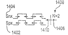
図3は、ブーストスイッチのペア(第1のブーストスイッチ(Sp)236および第2のブーストスイッチ(Sn)246)の動作を示すタイミング図である。第1の変調波形302は、第1のブーストスイッチ(Sp)236を表し、第2の変調波形304の動作は、第2のブーストスイッチ(Sn)246の動作を表す。第1および第2の変調波形302および304は、実質的にパルスの中心の共通タイムを共有し、かつ対称的に変調し、これにより、これらの波形のデューティサイクルの和がほぼ1の定数であるPWM信号である。
FIG. 3 is a timing diagram showing the operation of a pair of boost switches (first boost switch (Sp) 236 and second boost switch (Sn) 246). The
示された変調波形において、パワーソース112(図2)からの入力電圧(Vin)は、どちらかというと負であり、正になり得る。このような遷移は、第1および第2の変調波形302および304上の矢印によって示されるデューティおよびデューティトレンドを確立する。
In the modulation waveform shown, the input voltage (Vin) from the power source 112 (FIG. 2) is rather negative and can be positive. Such a transition establishes the duty and duty trend indicated by the arrows on the first and
図3は、変調位相図306をさらに含む。変調位相図306は、第1の変調波形302の変調を表す第1のベクトル308と、第2の変調波形304の変調を表す第2のベクトル310とを備える。図3に示される変調波形302および304は、変調位相図306の周囲で約180度均等に間隔を空けて離れる。
FIG. 3 further includes a modulation phase diagram 306. The modulation phase diagram 306 comprises a
図2において、第1および第2のブーストインダクタ(Lp、Ln)234および244の第1の側は、パワーソース112からのフィーダライン212と電気的に結合される。第1および第2のブーストインダクタ(Lp、Ln)234および244の第2の側は、各々第1および第2のブーストスイッチ(Sp、Sn)236および246の第1の側、ならびに各々第1および第2のブーストダイオード(Dp、Dn)238および248の一方の側と電気的に結合される。第1および第2のブーストスイッチ(Sp、Sn)236および246の他方の側は、各々第2および第1のブーストダイオード(Dn、Dp)248および238の他方の側、各々第1および第2のブーストキャパシタ(CpおよびCn)240および250の第1の側、ならびに各々第1および第2のブースト電圧出力ライン252および254と結合される。第1および第2のブーストキャパシタ(CpおよびCn)240および250の他方の側は、ブースト中心点256と電気的に結合される。ブースト中心点256は、さらに、コモンライン214と電気的に結合される。
In FIG. 2, first sides of first and second boost inductors (Lp, Ln) 234 and 244 are electrically coupled to
第1および第2のブーストインダクタ(Lp、Ln)234および244は、第1および第2のブーストスイッチ(Sp、Sn)236および246の動作によって磁化および消磁される。第1および第2のブーストインダクタ(Lp、Ln)234および244を磁化するためのパワーは、パワーソース112から、および、第1および第2のブーストキャパシタ(CpおよびCn)240および250からも提供される。第1および第2のブーストスイッチ(Sp、Sn)236と246は、第1および第2のブーストインダクタ(Lp、Ln)234と244と第1および第2のブーストキャパシタ(Cp、Cn)Lp)240と250との間に、接続される。従って、第1ブーストキャパシタ(Cp)240に蓄積される電圧は、パワーソース212からの利用可能な電圧が第1のブーストインダクタ(Lp)234を磁化するように寄与し得る。同様に、第2のブーストキャパシタ(Cn)250に蓄積される電圧は、パワーソース212からの利用可能な電圧が第2のブーストインダクタ(Ln)244を磁化するように寄与し得る。
The first and second boost inductors (Lp, Ln) 234 and 244 are magnetized and demagnetized by the operation of the first and second boost switches (Sp, Sn) 236 and 246. The power to magnetize the first and second boost inductors (Lp, Ln) 234 and 244 is provided from the
第2のブーストキャパシタ(Cn)250に蓄積されたエネルギーは、第1のブーストインダクタ(Lp)234の消磁から導出される。同様に、第1のブーストキャパシタ(Cp)240に蓄積されたエネルギーは、第2のブーストインダクタ(Ln)244の消磁から導出される。第1のブーストインダクタ(Lp)234は、正のインダクタ電圧と負の電流(例えば、V−I平面の第4象現)で磁化される。負の電流は、入力段202から出てパワーソース212に流れるという規則が理解されるべきである。さらに、第1および第2のブーストインダクタ(Lp、Ln)234および264の各々の正端子は、第1および第2のブーストスイッチ(Sp、Sn)236および246と各々電気的に結合される。
The energy stored in the second boost capacitor (Cn) 250 is derived from the demagnetization of the first boost inductor (Lp) 234. Similarly, the energy stored in the first boost capacitor (Cp) 240 is derived from the demagnetization of the second boost inductor (Ln) 244. The first boost inductor (Lp) 234 is magnetized with a positive inductor voltage and a negative current (eg, the fourth quadrant of the V-I plane). It should be understood that the negative current leaves the
従って、第1のブーストスイッチ(Sp)236が開いているとき(第1のブーストインダクタ(Lp)234の消磁モード)に、電流は、コモンライン214から第2のブーストキャパシタ(Cn)250、第1のブーストダイオード(Dp)238および第1のブーストインダクタ(Lp)234を通ってフィーダリン212に流れる。他方、第2のブーストインダクタ(Ln)244は、負のインダクタ電圧および正の電流(例えば、第2の象現)であるエネルギーで磁化される。従って、第2のブーストスイッチ(Sn)246が開いているときに、正の電流は、フィーダライン212から第2のブーストインダクタ(Ln)244、第2のブーストダイオード(Dn)248および第1のブーストキャパシタ(Cp)240を通ってコモンライン214に流れる。
Therefore, when the first boost switch (Sp) 236 is open (the demagnetization mode of the first boost inductor (Lp) 234), the current flows from the
第1のブーストインダクタ(Lp)234の消磁は、第1のブーストスイッチ(Sp)236が開いているときに開始し、電流が、第1のブーストダイオード(Dp)238を通って第1のブーストインダクタ(Lp)234から第2のブーストキャパシタ(Cn)250に流れ込むことを可能にする。第1のブーストインダクタ(Lp)234の消磁が終了し、そして、第1のブーストスイッチ(Sp)236が閉じていると磁化が再開する。同様に、第2のブーストスイッチ(Sn)246が開くと、第2のブーストインダクタ(LN)244の消磁が開始し、第2のブーストインダクタ(Ln)244からの電流が第2のブーストダイオード(Dn)248を通って流れ第1のブーストキャパシタ(Cp)240に流れ込むことが可能になる。 Demagnetization of the first boost inductor (Lp) 234 begins when the first boost switch (Sp) 236 is open, and the current passes through the first boost diode (Dp) 238 and the first boost It is possible to flow from the inductor (Lp) 234 to the second boost capacitor (Cn) 250. When the demagnetization of the first boost inductor (Lp) 234 is completed and the first boost switch (Sp) 236 is closed, the magnetization resumes. Similarly, when the second boost switch (Sn) 246 is opened, the demagnetization of the second boost inductor (LN) 244 starts, and the current from the second boost inductor (Ln) 244 becomes the second boost diode ( Dn) 248 can flow into the first boost capacitor (Cp) 240.
第2のブーストインダクタ(Ln)244の消磁が終了し、そして、第2のブーストスイッチ(Sn)246が閉じていると磁化が再開する。第1のブーストインダクタ(Lp)236が大きい負のインダクタ電流または正の入力電流(Iin)を搬送すべき場合にはいつでもパワーソース212がサイクルの負の部分にあるという事実によって磁化が促進される。同様に、第2のブーストインダクタ(Ln)246が大きい正のインダクタ電流または負の入力電流(Iin)を搬送すべき場合にいつでもライン112がサイクルの正の部分にある。入力電圧(Vin)が実質的に、入力電流(Iin)と同じ波形である場合、コンバータが抵抗負荷として機能した結果として高力率になる。
When the demagnetization of the second boost inductor (Ln) 244 is completed and the second boost switch (Sn) 246 is closed, the magnetization is resumed. Magnetization is facilitated by the fact that the
効率的な磁化サイクルは、入力電流(Iin)スルーレートが制限されることなく、第1および第2のブーストインダクタ(Lp、Ln)234および244のより大きい値のブーストインダクタンスの使用を可能にする。より大きい値のブーストインダクタンスを用いることによって、パワーソース112に印加されるリップル電流を低減する。第1および第2のブーストキャパシタ(Cp、Cn)240および250に蓄積された電圧は、パワーソース112によって供給される最大ピーク電圧よりも大きくなる。こうならない場合、入力電圧(Vin)がピークの間、意図されない電流が第1および第2のブーストダイオード(Dp、Dn)238および248を通って流れる。
An efficient magnetization cycle allows the use of higher values of boost inductance of the first and second boost inductors (Lp, Ln) 234 and 244 without limiting the input current (Iin) slew rate. . By using a larger value of boost inductance, the ripple current applied to the
従って、第1および第2のブーストキャパシタ(Cp、Cn)240および250の電圧は、入力電圧(Vin)を越えるようにブーストされる。例えば、約265V RMSの高さのライン電圧(Vin)での動作は、個々の第1および第2のブーストキャパシタ(Cp、Cn)の電圧が約380VDC〜約400VDCになるようにブーストされることを必要とし得る。この例において、ブーストスイッチ(Sp)236および(Sn)246ならびにブーストダイオード(Dp)238および(Dn)248は、全電圧の約760〜約800VDCに曝され得る。 Accordingly, the voltages of the first and second boost capacitors (Cp, Cn) 240 and 250 are boosted to exceed the input voltage (Vin). For example, operation with a line voltage (Vin) as high as about 265V RMS is boosted so that the voltage of the individual first and second boost capacitors (Cp, Cn) is between about 380 VDC and about 400 VDC. You may need. In this example, boost switches (Sp) 236 and (Sn) 246 and boost diodes (Dp) 238 and (Dn) 248 may be exposed to a total voltage of about 760 to about 800 VDC.
第1および第2のブーストキャパシタ(Cp、Cn)240および250に提供されたPWM電圧(Vc)およびピーク充電電流(Ic)は、第1および第2のブーストスイッチ(Sp、Sn)236および246の連係動作によって生成された正弦波形である。振幅、従って、PWM電圧(Vc)の波形の平均値もまた、第1および第2のブーストスイッチ(Sp、Sn)236および246の連係動作によって制御され得る。さらに、PWM電圧(Vc)の大きさ、従って、ピーク充電電流(Ic)の大きさは、第1および第2のブーストスイッチ(Sp、Sn)236および246の連係動作によって制御され得る。 The PWM voltage (Vc) and the peak charging current (Ic) provided to the first and second boost capacitors (Cp, Cn) 240 and 250 are the first and second boost switches (Sp, Sn) 236 and 246, respectively. It is a sine waveform generated by the linkage operation. The amplitude, and thus the average value of the PWM voltage (Vc) waveform, can also be controlled by the coordinated operation of the first and second boost switches (Sp, Sn) 236 and 246. Further, the magnitude of the PWM voltage (Vc), and thus the magnitude of the peak charge current (Ic), can be controlled by the coordinated operation of the first and second boost switches (Sp, Sn) 236 and 246.
起動中、ブーストキャパシタ(Cp、Cn)240および250の第1の充電が、パワーソース112のライン電圧(Vin)および低周波ピーク充電電流(Ic)から行われ得る。ピーク充電電流(Ic)は、第1および第2のブーストインダクタ(Lp、Ln)234および244、ならびに第1および第2のフリーホイーリングブーストダイオード(Dp、Dn)238および248を通って流れ得る。対向電流コンバータ230は、初期ブースト電圧(Vboost)を生成するためにPWM電圧(Vc)の生成の動作を行う必要がない。第1および第2のブーストキャパシタ(Cp,Cn)240および250の初期充電から生じる突入電流は、ソフトスタート回路222で穏やかにされ得る。第1の起動スイッチ224を閉じ、かつ、第2の起動スイッチ226を開いたままの状態にすることによって、突入電流を穏やかにするために抵抗器228のインピーダンスが用いられ得る。後続の起動で、第2の起動スイッチ226が閉じられ得る。故障状態が生じた場合、第1の起動スイッチ224および第2の起動スイッチ226の両方が開かれて、パワーソース112からの入力電流(Iin)の流れを停止させるように動作され得る。
During start-up, a first charge of boost capacitors (Cp, Cn) 240 and 250 may be taken from the line voltage (Vin) and low frequency peak charge current (Ic) of
示された力率補正パワーサプライ100において、対向電流コンバータ230は、入力電圧(Vin)に直接結合される。ブリッジ整流器段は用いられない。従って、第1および第2のブーストスイッチ(Sp、Sn)236および246にわたるピークツーピーク入力電圧(Vin)は、ブリッジ整流器段によって整流された入力電圧(Vin)の大きさの2倍の大きさである。
In the power factor corrected
第1および第2のブーストスイッチ(Sp、Sn)226および246が実質的に同じ時間中心で動作されるので、入力電圧(Vin)波形の低電圧部分を正確にトラッキングし、かつPWM電圧(Vc)を生成するためのさらなるスイッチ、インダクタおよび/またはキャパシタは必要でなく、かつ、力率補正パワーサプライ100内のブリッジ整流器段がないので、損失が低減される。絶縁されたゲートバイポーラトランジスタ(IGBT)または他のタイプのデバイス等の高電圧スイッチ技術は、より高いピークツーピーク入力電圧(Vin)を許容するために、第1および第2のブーストスイッチ(Sp、Sn)236および246に利用され得る。あるいは、ソフトスイッチングまたはゼロ電圧スイッチング(ZVS)は、より低速の高電圧スイッチ技術で利用され得る。
Since the first and second boost switches (Sp, Sn) 226 and 246 are operated at substantially the same time center, the low voltage portion of the input voltage (Vin) waveform is accurately tracked and the PWM voltage (Vc No additional switches, inductors and / or capacitors to generate) are required, and since there is no bridge rectifier stage in the power factor correcting
対向電流コンバータ230の出力電圧は、第1のブーストキャパシタ(Cp)240および第2のブーストキャパシタ(Cn)250の両方に提供される。対向電流コンバータ230の出力電圧は、ブースト電圧(Vboost)とも呼ばれ得る。第1のブーストキャパシタ(Cp)240と第2のブーストキャパシタ(Cn)250の各々のブースト電圧(Voost)は、約380VDC〜約400VDC等の相対的に高いDC電圧であり得る。相対的に高いDC電圧は、第1および第2のブーストインダクタ(Lp、Ln)234および244によって各々提供されるPWM電圧(Vc)およびピーク充電電流(Ic)によって、第1および第2のブーストキャパシタ(Cp、Cn)240および250を充電することによって達成され得る。
The output voltage of the counter
第1および第2のブーストスイッチ(Sp、Sn)236および246のデューティサイクルでのスイッチングにより、第1および第2のブーストインダクタ(Lp、Ln)234および244を磁化および消磁される。第1および第2のブーストキャパシタ(Cp、Cn)240および250を充電するための所望の位相および大きさのPWM電圧(Vc)波形がデューティサイクルの制御によって生成される。第1および第2のブーストキャパシタ(Cp、Cn)240および250は、各々、ブースト電圧(Voost)に充電される。第1および第2のブーストキャパシタ(Cp、Cn)240および250の各々は、ブースト電圧(Vboost)に別々に充電されるので、対向電流コンバータ230は、約760VDC〜約800VDC等の、このブースト電圧(Vboost)の約2倍にされ得る。
Switching at the duty cycle of the first and second boost switches (Sp, Sn) 236 and 246 magnetizes and demagnetizes the first and second boost inductors (Lp, Ln) 234 and 244. A PWM voltage (Vc) waveform of the desired phase and magnitude for charging the first and second boost capacitors (Cp, Cn) 240 and 250 is generated by duty cycle control. The first and second boost capacitors (Cp, Cn) 240 and 250 are each charged to a boost voltage (Vost). Since each of the first and second boost capacitors (Cp, Cn) 240 and 250 are separately charged to the boost voltage (Vboost), the counter
ブースト比は、ブースト電圧(Vboost)を入力電圧(Vin)の瞬時値で割ることによって決定され得る。比較的低い入力電圧(Vin)(日本における100VAC定格等)では、所望のブースト電圧(Vboost)を達成するためにより高いブースト比が必要とされる。しかしながら、対向電流コンバータ230に関しては、第1および第2のブーストスイッチ(Sp、Sn)236および246、ならびに第1および第2のブーストダイオード(Dp、Dn)238および248のデューティサイクルは、高出力パワーおよび低入力ライン電圧(例えば、高ブースト比)で約50%に収斂する。他方、いくつかのブーストコンバータは、ダイオードのデューティサイクルがゼロに達するという痛手を受けるが、スイッチデューティサイクルは、高ブースト比を生成するために、低電圧で100%になる。
The boost ratio can be determined by dividing the boost voltage (Vboost) by the instantaneous value of the input voltage (Vin). At relatively low input voltages (Vin) (such as 100 VAC rating in Japan), higher boost ratios are required to achieve the desired boost voltage (Vboost). However, for the counter
第1および第2のブーストインダクタ(Lp、Ln)234および244は、パワーソース112と、第1および第2のブーストキャパシタ(Cp、Cn)240および250との両方によって磁化されるので、スイッチデューティサイクルは、著しく低くなり得る。さらに、フライバックおよび共振コンバータと比較して、対向電流コンバータ230によってでは入力電流(Iin)の高ピーク電流は見られない。高ピーク電流は、第1および第2のブーストインダクタ(Lp、Ln)234および244のより大きいインダクタンスで回避され得る。なぜなら、第1および第2のブーストインダクタ(Lp、Ln)234および244を完全に磁化するために十分なパワーが利用可能であるので、スイッチデューティサイクルの間の不十分な磁化および消磁をほとんど気にせずに、インダクタンスが増加され得る。不十分な磁化および消磁は、いくつかのブーストコンバータにおいて、低瞬時入力電圧で著しいライン電流の歪みを引き起こし得る。
Since the first and second boost inductors (Lp, Ln) 234 and 244 are magnetized by both the
過渡ピーク入力電圧耐性(voltage immunity)は、さらに、第1および第2のブーストインダクタ(Lp、Ln)234および244のインダクタンスの大きさに基づいて対向電流コンバータ230によって提供され得る。過渡ピーク入力電圧が第1および第2のブーストインダクタ(Lp、Ln)234および244を有意に磁化するには持続が不十分である場合、ダメージなく、大きい過渡電圧が可能である。有意な磁化(significant magnetization)は、第1および第2のブーストキャパシタ(Cp、Cn)240および250を過充電するための十分に大きい大きさを有するピーク充電電流(Ic)を生成する磁化の量である。
Transient peak input voltage immunity may also be provided by the counter
第1および第2のブーストインダクタ(Lp、Ln)234および244のインダクタンスは、さらに、循環電流および静止スイッチング損失を最小にするために十分な大きさに設計され得る。例えば、力率補正パワーサプライ100の50/60Hzのインダクタンスは、広帯域幅オーディオ増幅器設計によって必要とされるインダクタンス(従って、パワー)の大きさよりもはるかに大きくなり得る。第1および第2のブーストインダクタ(Lp、Ln)234および244のサイズへの制限は、物理サイズ制限およびインダクタパワー損失(I2R)によって管理され得る。いくつかのブーストコンバータにおいて、大きいインダクタンスを使用すると、低パワー入力でありながら、入力電圧(Vin)と入力電流(Iin)との谷に入力波形の歪みが生じることにも留意されたい。対向電流コンバータ230に関しては、このような歪みは生じない。なぜなら、対向電流コンバータ230は、真のAC入力コンバータだからである。
The inductances of the first and second boost inductors (Lp, Ln) 234 and 244 can be further designed to be large enough to minimize circulating current and quiescent switching losses. For example, the 50/60 Hz inductance of the power factor correcting
第1および第2のブーストインダクタ(Lp、Ln)234および244のインダクタンスの物理サイズおよび大きさは、力率補正パワーサプライ100によって供給される負荷の動作特性を考慮に入れることによっても決定され得る。例えば、力率補正パワーサプライ100は、オーディオ増幅器である負荷に供給する場合、第1および第2のブーストインダクタ(Lp、Ln)234および244の物理サイズはより小さくなり得る。オーディオ増幅器の平均パワーサプライが、通常、オーディオ増幅器のピーク需要電力よりもはるかに小さいので、それらのサイズを最小化するために第1および第2のブーストインダクタ(Lp、Ln)234および244の低速熱時定数(slow thermal time constant)が利用され得る。この例において、第1および第2のブーストインダクタ(Lp、Ln)234および244は、定格ベンチパワーサイジングよりも小さめであり得る。過小寸法である場合、第1および第2のブーストインダクタ(Lp、Ln)234および244は、また、温度過昇状態を防止するためにモニタリンクされ得る。
The physical size and magnitude of the inductances of the first and second boost inductors (Lp, Ln) 234 and 244 can also be determined by taking into account the operating characteristics of the load supplied by the power factor correcting
PFCコントローラ232は、対向電流コンバータ230が力率補正および電圧レギュレーションを実行するように方向付けることができる回路またはデバイスであり得る。対向電流コンバータ230を方向付けることは、第1および第2のブーストスイッチ(Sp、Sn)236および246のスイッチングデューティ(デューティサイクル)を制御することを包含する。デューティサイクルの活性部分(activation portion)は、実質的に同じ時間中心を維持する。換言すると、第1および第2のブーストスイッチ(Sp、Sn)236および246は、PFCコントローラ232によって各デューティサイクルの一部分の間に同時に活性化される。PFCコントローラ232は、第1のスイッチ制御ライン258および第2のスイッチ制御ライン260で、第1および第2のブーストスイッチ(Sp、Sn)236および246を各々選択的に活性化および不活性化し得る。第1および第2のブーストスイッチ(Sp、Sn)236および246のデューティサイクルは、PFCコントローラ232によって感知された電圧および電流に基づいてPFCコントローラ232によって方向付けられ得る。
The
示されたPFCコントローラ232は、入力電圧感知ライン262上の対向電流コンバータ230への入力電圧(Vin)を感知する。入力電圧(Vin)は、フィーダライン212とコモンライン214との間で測定されることによって、対向電流コンバータ230の入力側で測定され得る。パワーソース112から流れる入力電流(Iin)の大きさおよび波形は、AC電流を感知するための電流変圧器、ロゴスキーコイル(Rogowski coil)、抵抗分路器、または、任意の他のメカニズムといった電流センサ264で測定され得る。電流センサ264は、入力電流感知ライン266上で測定された入力電流(Iin)をPFCコントローラ232に提供し得る。測定された入力電流(Iin)は、スケーリングファクタ(Ka)でスケーリングされ、スケーリングして測定された入力電流(Ka*Iin)を形成し得る。
The illustrated
正のDCレール106および負のDCレール108上の正のDC出力電圧(+Vcc)および負のDC出力電圧(−Vcc)は、さらに、正のVcc感知ライン268および負のVcc感知ライン270上のPFCコントローラ232によって各々感知される。PFCコントローラ232は、さらに、ブースト電圧感知ライン272上の対向電流コンバータ230のブースト電圧(Vboost)を感知し得る。ブースト電圧(Vboost)は、第1のブースト電圧出力ライン252と第2のブースト電圧出力ライン254との間で測定することによって対向電流コンバータ230の出力側にわたって測定され得る。
The positive DC output voltage (+ Vcc) and the negative DC output voltage (−Vcc) on the
PFCコントローラ232による力率補正は、パワーソース112から対向電流コンバータ230に供給されたAC入力電流(Iin)の正弦波形の調整を暗黙的に含む。AC入力電流(Iin)の正弦波形は、第1および第2のブーストキャパシタ240および250に供給されたPWM電圧(Vc)の正弦波形に対する調整によって暗黙的に調整される。PWM電圧(Vc)の波形は、第1および第2のブーストスイッチ(Sp、Sn)236および246をスイッチングして、対向電流コンバータ230に供給されたAC入力電圧(Vin)の正弦波形と実質的に同一である平均波形を維持することによって調整される。
The power factor correction by the
PWM電圧(Vc)の平均波形を入力電圧(Vin)の正弦波形と実質的に同じものとして維持することによって、高調波が最小化され、力率が改善される。PWM電圧(Vc)および入力電圧(Vin)の波形が実質的に同一である場合、入力電流(Iin)の波形も入力電圧(Vin)の正弦波形の形状と実質的に同一である。従って、力率補正パワーサプライ100は、パワーソース112の観点から、実質的に抵抗負荷として見える。
By maintaining the average waveform of the PWM voltage (Vc) substantially the same as the sine waveform of the input voltage (Vin), the harmonics are minimized and the power factor is improved. When the waveforms of the PWM voltage (Vc) and the input voltage (Vin) are substantially the same, the waveform of the input current (Iin) is also substantially the same as the shape of the sine waveform of the input voltage (Vin). Thus, the power factor corrected
他方、電圧レギュレーションは、力率補正パワーサプライ100上の入力電圧(Vin)と負荷とが変動する場合の、PFCコントローラ232の全電圧ゲインを制御することを包含する。電圧ゲインの制御は、第1および第2のブーストスイッチ(Sp、Sn)236および246のスイッチングを制御して、PWM電圧(Vc)、従って、ブーストキャパシタ(Cp、Cn)240および250に供給されるピーク充電電流(Ic)の大きさを制御することを包含する。対向電流コンバータ230のPWM電圧(Vc)の大きさは、正のDCレール106および負のDCレール108上で所望の電圧を維持するように変更され得る。
On the other hand, voltage regulation includes controlling the total voltage gain of the
上述のように、対向電流コンバータ230は、「バックワード」増幅器として動作する。(ブースト電圧(Vboost)を介して)DCレールにDC出力パワーを供給するために、パワーソース112は、入力電流(Iin)を対向電流コンバータ230に「押し込む(push)」。入力電流(Iin)を流し込むために、入力電圧(Vin)の大きさは、「トラッキングゲイン比(tracking gain ratio)」に基づいてPWM電圧(Vc)の相対大きさを超えるように維持される。「トラッキングゲイン比」は、平均AC PWM電圧(Vc)の大きさに対するAC入力電圧(Vin)の大きさの所望の比として定義される。PWM電圧(Vc)は、対向電流コンバータ230によって、第1および第2のブーストキャパシタ(Cp、Cn)240および250をブースト電圧(Vboost)に充電することによって生成される。
As described above, the counter
入力電圧(Vin)の相対大きさがPWM電圧(Vc)の大きさと(トラッキングゲイン比に基づいて)実質的に同じである場合、対向電流コンバータ230に流れ込む入力電流(Iin)の大きさは最小である。PWM電圧(Vc)の大きさが(トラッキングゲイン比に基づいて)入力電圧(Vin)の相対大きさよりも低くなると、対向電流コンバータ230に流れ込む入力電流(Iin)の大きさが比例的に増加する。同様に、入力電圧(Vin)の相対大きさに対してPWM電圧(Vc)の大きさが(トラッキングゲイン比に基づいて)増加すると、対向電流コンバータ230に流れ込む入力電流(Iin)の大きさが減少する。
When the relative magnitude of the input voltage (Vin) is substantially the same as the magnitude of the PWM voltage (Vc) (based on the tracking gain ratio), the magnitude of the input current (Iin) flowing into the counter
図4は、Texas Instruments/Unitrode UC3854と類似のPFCコントローラ232の例である。示されたPFCコントローラ232は、差動増幅器402、入力電圧フィードフォワード制御ループ404、出力電圧フィードバック制御ループ406および電流制御内部ループ408を備える。差動増幅器402は、スケーリングファクタ(Kin)で動作し、入力電圧感知ライン262上で受け取られた入力電圧(Vin)を所定の電圧の大きさにスケーリングする。スケーリングされた入力電圧(Kin*Vin)は、その後、入力電圧フィードフォワード制御ループ404および出力電圧フィードバック制御ループ406に供給される。
FIG. 4 is an example of a
入力電圧フィードフォワード制御ループ404は、ローパス(LP)フィルタ412、二乗乗算器414、および除算器416を備える。LPフィルタ412は、スケーリングされた入力電圧(Kin*Vin)のDCまたは平均値を抽出するように動作する。LPフィルタ412は、入力電圧(Vin)の平均値を抽出する前に、入力電圧(Vin)の整流も含み得る。ブリッジ整流器が入力段パワーコンバータ202(図2)の前に含まれる場合、入力電圧(Vin)は極性を変更せず、従って、LPフィルタ412で整流される必要がない。二乗乗算器414は、LPフィルタ412によって提供されるスケーリングされた入力電圧(Kin*Vin)の平均値を二乗する。スケーリングされた入力電圧(Kin*Vin)の二乗した値が除算器416の分母として提供される。
The input voltage
第1および第2のブーストスイッチ236および246(図2)のデューティサイクルは、入力電圧フィードフォワード制御ループ404で制御され得る。デューティサイクルは、パワーソース112(図1)から力率補正パワーサプライ100に提供された入力電圧(Vin)の範囲に基づいて制御され得る。従って、入力電圧フィードフォワード制御ループ404は、変化する入力電圧(Vin)に対して、定常的平均入力パワーで機能する入力段パワーコンバータ202(図2)を保持する1つのフィードフォワード技術を提供する。他の例において、同様の機能を達成するために他の技術が用られてもよい。
The duty cycle of the first and second boost switches 236 and 246 (FIG. 2) may be controlled by the input voltage
出力電圧フィードバック制御ループ406は、差動入力増幅器420、加算器422、積分器424、および乗算器426を備える。差動入力増幅器420は、正のVcc感知ライン268から正のDC出力電圧(+Vcc)、および、負のVcc感知ライン270から負のDC出力電圧(−Vcc)を受け取る。差動入力増幅器420は、正のDC出力電圧(+Vcc)および負のDC出力電圧(−Vcc)の差をスケーリングし得る。
The output voltage
単相の応用例において、差動入力増幅器420は、所定のゲイン定数(Kf)をさらに備え得る。ゲイン定数(Kf)は、差動入力増幅器420の出力電圧を差動入力増幅器420の動作電圧と適合するようにスケーリングし得る。スケーリングされたバージョンの所望のDC出力電圧(Vref)は、加算器422によってスケーリングされた差動電圧(2*Kf*Vcc)から引かれる。出力電圧フィードバック制御ループ406の応答速度をかなり大きくすると、単相回路におけるライン電流の歪みは実質的に低下され得る。従って、制御は、積分器424によって減速されてもよい。積分器424は、積分器424の出力に比例項を含むことによって、比例積分器(PI)コントローラとしても動作し得る。加算器422の出力は、積分器424によって積分され、かつ、電圧誤差補償信号(Verr)として乗算器426に提供される。
In a single phase application, the
電圧誤差補償信号(Verr)は、実際のDC出力電圧(+Vcc、−Vcc)と基準電圧(Vref)との間の誤差電圧を表す高度にフィルタリングされた信号である。乗算器426は、電圧誤差補償信号(Verr)とスケーリングされた入力電圧(Kin*Vin)を乗算する。乗算器426は、さらに、ゲイン係数を調整するためにゲイン定数(Km)も含み得る。その結果が分子として除算器416に提供され、スケーリングされた入力電圧(Kin*Vin)の二乗値によってスケーリングされる。除算器416は、所望の電流波形(Id)のスケーリングされたバージョンを生成する。所望の電流波形(Id)は、実質的に1の力率を達成し得る電流波形である。所望の電流波形(Id)は、電流制御内部ループ408に提供される。 The voltage error compensation signal (Verr) is a highly filtered signal representing the error voltage between the actual DC output voltage (+ Vcc, -Vcc) and the reference voltage (Vref). The multiplier 426 multiplies the voltage error compensation signal (Verr) by the scaled input voltage (Kin * Vin). Multiplier 426 may also include a gain constant (Km) to adjust the gain factor. The result is provided as a numerator to divider 416 and scaled by the square value of the scaled input voltage (Kin * Vin). Divider 416 generates a scaled version of the desired current waveform (Id). The desired current waveform (Id) is a current waveform that can achieve a power factor of substantially one. The desired current waveform (Id) is provided to the current control inner loop 408.
電流制御内部ループ408は、加算器430、誤差増幅器432、およびスイッチコントローラ434を備える。加算器430は、入力電流感知ライン266上で受け取られたスケーリングされた測定入力ライン電流(Ka*Iin)を所望の電流波形(Id)から引いて、電流誤差信号(Ie)を生成する。誤差増幅器は、電流誤差信号(Ie)を形成するために積分し、かつ、比例誤差を提供して、スイッチコントローラ434を駆動し、ピーク充電電流(Ic)およびPWM電圧(Vc)を生成する。スイッチコントローラ434は、比例誤差によって駆動され、対向電流コンバータ230通じてのトランスコンダクタンスを制御することによって、対向電流コンバータ230(図2)の実効入力インピーダンスを制御する。
The current control inner loop 408 includes an
対向電流コンバータ230の実効入力インピーダンスは、入力電流(Iin)で除算された入力電圧(Vin)から引かれたPWM電圧(Vc)である。実効入力インピーダンスの制御は、AC入力電流(Iin)の波形の位相制御、従って、力率を制御する。負の電流フィードバックの適度な量は、対向電流パワーコンバータ230(図2)の実効入力インピーダンスの増大の効果を有し得る。対向電流コンバータ230の実効入力インピーダンスの変動が、第1および第2のブーストスイッチ(Sp、Sn)236および246のデューティサイクルによって達成され得る。デューティサイクルは、トランスコンダクタンス、従って、対向電流コンバータ230の実効入力インピーダンスを調整するように選択的に変化され得る。
The effective input impedance of the counter
図4に示されるPFCコントローラ232に関して、トランスコンダクタンスの制御は、主に、内部電流制御ループ408の入力ライン電流(Iin)に基づく。PWM電圧(Vc)と入力電圧(Vin)との大きさの差は、入力電流(Iin)の流れに基づいて決定され得る。換言すると、PWM電圧(Vc)(例えば、より高い電圧ゲイン)の大きさがより大きいと、結果的にはピーク充電電流(Ic)をより低くする。同様に、PWM電圧(Vc)(例えば、より低いゲイン)の大きさがより小さいと、ピーク充電電流(Ic)がより高くなる。入力ライン電流(Iin)の大きさに基づいて、PFCコントローラ232の全電圧ゲインは調整され得る。
With respect to the
スイッチコントローラ434は、パルス幅変調(PWM)変調器436、および、対向電流コンバータ230のブーストスイッチを駆動するための複数のゲートドライバ438を備え得る。図2に示される例において、PWM電圧(Vc)の大きさを制御するために第1および第2のブーストスイッチ(Sp、Sn)236および246が駆動される。第1および第2のブーストスイッチ(Sp、Sn)236および246(図2)は、第1のスイッチ制御ライン258および第2のスイッチ制御ライン260を介して各々駆動され得る。
The
対向電流コンバータ230を駆動するために、PWM変調器436は、ダブルエッジ自然PWMで動作し、インターリーブの使用を最適化し得る。ダブルエッジ自然PWMにおいて、変調する波形は三角波形であり、変調された信号は、時間の連続変数である。従って、PWM変調器は、Nのインターリーブで動作し、ここで、Nは、ブーストスイッチおよびゲートドライバ438の数である。示される例において、対向電流コンバータ230(図2)は、2つのブーストスイッチ(第1および第2のブーストスイッチ(Sp、Sn)236および246)を備え、従って、N=2である。他の例において、さらなるブーストスイッチが含まれてもよい。
To drive the counter
図5は、図4を参照して記載されたものとは異なった制御構造を有するPFCコントローラ232の別の例である。簡略化するために、以下の記載は、これらの差異に的を絞る。この例において、電圧ゲインは、入力電圧(Vin)に基づいてPFCコントローラ232によって主に制御される。図5のPFCコントローラ232は、差動増幅器402、入力電圧フィードフォワード制御ループ502、出力電圧フィードバック制御ループ504、および電圧制御内部ループ506を備える。差動増幅器402は、スケーリングされた入力電圧(Kin*Vin)を入力電圧フィードフォワード制御ループ502に含まれる加算器510に提供する。
FIG. 5 is another example of a
出力電圧フィードバック制御ループ504は、図4と同様に、差動増幅器420、加算器422および積分器424を備える。さらに、出力電圧フィードバック制御ループ504は、電圧誤差補償信号(Verr)とスケーリングされた入力電圧(Kin*Vin)を乗算する乗算器512を備える。その結果は、加算器510に提供される。加算器510は、電圧誤差補償信号(Verr*Km*Kin*Vin)およびスケーリングされた測定された入力電流(Ka*Iin)をスケーリングされた入力電圧(Kin*Vin)から引いて、電流誤差信号(Ie)を生成してスイッチコントローラ506を駆動する。スイッチコントローラ506は、PWM変調器516および複数のゲートドライバ518を備える。
The output voltage
図4のPWM変調器436と同様に、PWM変調器516は、対向電流コンバータ230におけるブーストスイッチのデューティサイクル(図2の例において、N=2)を方向付けるNのインターリーブで動作する。しかしながら、図5のPWM変調器516は、さらなるフィードフォワード制御ループをさらに備える。ブースト電圧感知ライン272上のブースト電圧(Vboost)は、フィードフォワード信号として、PWM変調器516に提供される。内部電圧制御ループ506は、PWM変調器516によって生成された変調波形のスケーリングの制御を提供する。変調する三角波形は、所望のブースト電圧(Vboost)に比例するようにスケーリングされ得る。さらなるフィードフォワード制御ループは、加算器510から提供された電流誤差信号(Ie)のゲイン安定化を提供する。
Similar to
電圧制御内部ループ506の電圧ゲインは、トラッキングゲイン比に基づいて固定され得る。従って、PWM変調器516のゲインは、ブーストキャパシタ上のブースト電圧(Vboost)の誤差を補償する逆数ゲインであり得る。このような補償がない場合、PWM変調器516のゲインは、ブーストキャパシタのブースト電圧(Vboost)に比例し、すなわち、固定されず、変化する。この制御法を用いて、PFCコントローラ232は、対向電流コンバータ230のPWM電圧(Vc)がブースト電圧(Vboost)に基づいて振幅制御された場合、電圧制御を提供するデューティとして線形である内部制御ループ(電圧制御内部ループ506)を備える。ゲイン安定化のための類似のタイプのフィードフォワード制御ループが、さらに、図4を参照して記載されたPFCコントローラ232で実装され得る。
The voltage gain of the voltage control inner loop 506 can be fixed based on the tracking gain ratio. Thus, the gain of the
図5の例示的PFCコントローラ232において、入力電圧フィードフォワード制御ループ502は、電圧制御内部ループ506への主な信号としてスケーリングされた入力電
圧(Kin*Vin)を確立する。電圧制御内部ループ506は、(1/Kin)の電圧ゲインを備える。電圧ゲイン(1/Kin)は、Kinを消去し、制御信号として入力電圧(Vin)のみを残して、負荷のない状態下でPWM電圧(Vc)を生成する。その結果、静止状態(例えば、力率補正パワーサプライへの負荷が小さいか、または無い)の間、第1のコンバータ段202(図2)は、PWM電圧(Vc)で入力電圧(Vin)をトラッキングし得る。入力電圧(Vin)は、トラッキングゲイン比に基づいて、PWM電圧(Vc)によってトラッキングされ得る。従って、対向電流コンバータ230は、デフォルトによってパワーを伝送し得ない。図5のPFCコントローラ232を用いる対向電流コンバータ230の動作は、動作の反転(reverse)増幅器の形態として記載され得る。反転増幅器の動作は、従来の増幅器動作の反対であり、そこでは、増幅器は、ここでの場合のように、入力をトラッキングするのではなく、期待された形態の出力を有するように駆動される。
In the
フィードフォワード制御ループは、主な制御信号としてスケーリングされた入力電圧(Kin*Vin)で動作するので、出力電圧フィードバック制御ループ504からの電圧誤差補償信号(Verr)の影響が最小化される。フィードフォワード制御が電圧制御内部ループ506によって提供されるため、力率補正パワーサプライ100(図1)の電圧レギュレーションを損なうことなく電圧誤差補償信号(Verr)が最小化され得る。ブースト電圧(Vboost)でのさらなるフィードフォワード制御の結果、乗算器512は、フィードフォワード制御信号の一部分のみを管理し得る。さらに、乗算器512は、ダイナミックレンジをあまり有しなくて良い。従って、乗算器512は、図4を参照して記載される乗算器426ほどには正確でなく、かつ高価でなくて良い。
Since the feedforward control loop operates with the scaled input voltage (Kin * Vin) as the main control signal, the influence of the voltage error compensation signal (Verr) from the output voltage
非静止状態の間、図5のPFCコントローラ232は、スケーリングされた、測定された入力電流(Ka*Iin)の形態での比較的適度な量の負の電流フィードバックを用いて、対向電流コンバータ230(図2)の実効入力インピーダンスを制御し得る。実効入力インピーダンスの制御は、上述のように、力率を制御する。
During the non-stationary state, the
さらに、非静止状態の間、全電圧ゲインは、力率補正パワーサプライ100(図1)のDC出力電圧(正および負のDC出力電圧(+Vccおよび−Vcc))をレギュレートするように調整され得る。上述のように、全電圧ゲインの調整は、出力フィードバック制御ループ504を通じて行われ得る。PFCコントローラ232の全電圧ゲインが変更されると、対向電流コンバータ230は、良好に制御されて、パワーソース112(図1)からパワーを取得するか、または、パワーソース112にパワーを戻し得る。
In addition, during non-stationary conditions, the total voltage gain is adjusted to regulate the DC output voltage (positive and negative DC output voltages (+ Vcc and −Vcc)) of the power factor correcting power supply 100 (FIG. 1). obtain. As described above, the adjustment of the total voltage gain can be made through the output
従って、入力段パワーコンバータ202は、第1象現および第3象現にてパワーソース112へのパワーのソースとして、かつ、第2および第4象現にてパワーソース112からのパワーを消費するように動作し得る。PFCコントローラ232は、1未満である全フィードフォワード増幅器ゲインを生成し、パワーは、対向電流コンバータ230に流れ込む。他方、全電圧ゲインが1を超える場合、パワーは、対向電流コントローラ232からパワーソース112に流れ出す。
Therefore, the input
PFCコントローラ232の全電圧ゲインを約1になるように変更するために、電圧ゲインの制御に寄与する乗算器512は、乗算器512のバイポーラ入力に提供された入力電圧(Kin*Vin)を有する、少なくとも1つの2象現分で動作する乗算器(2および4象現で動作する)であり得る。PFCコントローラ232の全電圧ゲインは、乗算器512および電圧制御内部ループ506を考慮しない場合、スケーリング増幅器402のスケーリングファクタ(Kin)または加算器510内のスケーリングを調整することによって、わずかに1を超えるように設定され得る。従って、全電圧ゲインを低減するために乗算器512が用いられ得る。
In order to change the total voltage gain of the
この制御方法において、乗算器512の必要とされる全作業範囲は、2象現分でよい。力率補正パワーサプライ100(図1)への負荷が増加すると、出力電圧フィードバック制御ループ504は、乗算器512にバイアスをかけて電圧誤差補償信号(Verr)で動作することが必要とされるに過ぎないから、乗算器512は2象現分でよい。パワーソース112にパワーを戻す必要が最小であるべきなので、乗算器512は、4象現分動作をサポートする必要がない。
In this control method, the required total working range of the
あるいは、乗算器512は、4象現動作をサポートし得る。従って、PFCコントローラ232は、パワーソース112(図1)にパワーを調達するか、または、これからのパワーを消費するように対向電流コンバータ230(図2)を制御し得る。4象現分動作をサポートする際に、PFCコントローラ232の全電圧ゲインは、乗算器512および電圧制御内部ループ506を考慮しない場合、実質的に1に設定され得る。その結果、乗算器512は、全電圧ゲインを1を超える、および1未満の両方に調整し得る。
Alternatively,
対向電流コンバータ230(図2)のブーストキャパシタが過剰なエネルギーを蓄積した場合、エネルギーは、パワーソース112(図1)に戻され得る。蓄積されるエネルギーが過剰になる主な原因は、パワーソース112のサージおよび出力電圧フィードバック制御ループ504または電圧制御内部ループ506における制御オーバーシュートであり得る。ブーストキャパシタ上の電圧が入力および出力コンバータ202および204(図2)にとって有害である場合、PFCコントローラ232は、電圧が安全なレベルに低下(bleed down)するまで対向電流コンバータ230のすべてのスイッチングをディセーブルし得る。
If the boost capacitor of the counter current converter 230 (FIG. 2) accumulates excess energy, the energy can be returned to the power source 112 (FIG. 1). The primary cause of excess stored energy may be a surge in the
図6は、さらに別の例示的PFCコントローラ232である。この例において、PFCコントローラ232は、図5と同様に、差動増幅器402、入力電圧フィードフォワード制御ループ502および電圧制御内部ループ506を備える。差動増幅器402、入力電圧フィードフォワード制御ループ502および電圧制御内部ループ506は、すべて、図5の例と同様に機能する。図6のPFCコントローラは、図5を参照して記載された出力電圧フィードバック制御ループ504と同様である出力電圧フィードバック制御ループ602をさらに備える。
FIG. 6 is yet another
しかしながら、出力電圧制御ループ602は、整流器604、ローパス(LP)フィルタ606、および加算器608を備える。整流器604、ローパスフィルタ606および加算器608は、測定された入力電流(Iin)を出力電圧フィードバック制御ループ602に導入する。測定された入力電流(Iin)は、スケーリングファクタ(Kb)でスケーリングされて、スケーリングされた測定入力電流(Kb*Iin)を形成し得る。
However, the output
スケーリングされた測定入力電流(Kb*Iin)は、整流器604に提供され得る。整流器604は、スケーリングされた測定入力電流(Kb*Iin)の整流を提供し得る。ブリッジ整流器が入力段パワーコンバータ202の前に備えられる場合のように、入力電流(Iin)がすでに整流されている場合、測定入力電流(Iin)は極性を変更せず、従って、整流器604は不必要である。整流、スケーリングされた測定入力電流(Kb*Iin)の平均は、LPフィルタ606によってフィルタリングされる。フィルタリングに続いて、フィルタリング、整流、スケーリングされた測定入力電流(Kb*Iin)は、加算器608によって電圧誤差補償信号(Verr)に加算され、DC出力電圧の(正および負のDC出力電圧(+Vccおよび−Vcc))「スーパーレギュレーション(super regulation)」を行う。
The scaled measured input current (Kb * Iin) may be provided to the
スーパーレギュレーションは、入力段パワーコンバータ202(図2)によって引き出された測定された入力電流(Iin)の平均値の大きさを感知することによって導出され得る。DC出力電圧(正および負のDC出力電圧(+Vccおよび−Vcc))は、その後、測定された入力電流(Iin)の平均値の大きさに応答して調整され得る。DC出力電圧が上昇した場合、この効果は、任意の実効供給インピーダンスを低下させ、従って、測定された入力電流(Iin)の平均値の大きさを増加させることである。同様に、DC出力電圧が低下した場合、実効供給インピーダンスは上昇し、測定された入力電流(Iin)の平均値の大きさは小さくなる。十分な電流フィードバックが行われた場合、DC出力電圧がパワーの流出の増加を伴って上昇する。このような応答は、負の出力抵抗を定義することによる。 Superregulation can be derived by sensing the average magnitude of the measured input current (Iin) drawn by the input stage power converter 202 (FIG. 2). The DC output voltages (positive and negative DC output voltages (+ Vcc and −Vcc)) can then be adjusted in response to the average magnitude of the measured input current (Iin). If the DC output voltage is increased, this effect is to reduce any effective supply impedance and thus increase the average magnitude of the measured input current (Iin). Similarly, when the DC output voltage decreases, the effective supply impedance increases and the average value of the measured input current (Iin) decreases. If sufficient current feedback is provided, the DC output voltage will rise with increasing power drain. Such a response is due to defining a negative output resistance.
電圧制御内部制御ループ506上で用いられる瞬時的な負の電流フィードバックの量は、スーパーレギュレーションによって増加され得る。しかしながら、図4に示されるPFCコントローラ232の電流制御内部ループ408等におけるような、比較的大量の瞬時的な負の電流フィードバックの場合には、スーパーレギュレーションは不必要である。しかしながら、図5および図6におけるような比較的少ない量の負の電流フィードバックの場合には、瞬間的な負の電流フィードバックを増加させることは小さいデューティ対電圧変換誤差から生じた入力電流(Iin)の歪みを低減する。入力段パワーコンバータ202(ブーストコンバータ)の入力インピーダンスが非常に低いので、PWM電圧(Vc)における小さい歪みは、入力電流(Iin)の大きい歪みとして表し得る。負の電流フィードバックを通じて第1のパワー段コンバータ202のインピーダンスを増加することにより、第1のパワー段コンバータ202の線形的要求が緩和され得る。しかしながら、DC出力電圧のレギュレーションは、影響され得る。
The amount of instantaneous negative current feedback used on the voltage control inner control loop 506 can be increased by super regulation. However, in the case of a relatively large amount of instantaneous negative current feedback, such as in the current control inner loop 408 of the
図5を参照して記載されたPFCコントローラ232と同様に、単相PFC回路におけるライン電流の歪みは、出力電圧フィードバック制御ループ602の過度に速い応答速度によって実質的に劣化される。従って、図5および図6に示されるPFCコントローラ234の出力電圧フィードバック制御ループ504および602の応答速度は、穏やかに遅くなり得る。しかしながら、この遅さが負荷または入力電圧(Vin)変化に対する応答を高速でトラッキングすることを難しくさせ得る。
Similar to the
図6のスーパーレギュレーションは、応答速度の改善を達成する。測定入力電流(Iin)の追加フィードバックもまた、早くなくても、入力電流(Iin)の歪みに加算することを避けるために、速すぎてもいけないが、改善された応答速度が達成され得る。制御補償信号のリップル(電圧誤差補償信号(Verr)および整流、スケーリングした測定入力電流(Kb*Iin))は、異なるように位相制御され得る。リップルは、正味リップルが、制御補償信号のどちらか1つによってもたらされたものよりも小さくなるように位相制御され得る。 The super regulation of FIG. 6 achieves an improved response speed. The additional feedback of the measured input current (Iin) must also be too fast to avoid adding to the distortion of the input current (Iin), if not early, but an improved response speed can be achieved. The ripple of the control compensation signal (voltage error compensation signal (Verr) and rectified, scaled measured input current (Kb * Iin)) can be phase controlled differently. The ripple may be phase controlled so that the net ripple is less than that provided by either one of the control compensation signals.
図2において、示された出力段パワーコンバータ204は、対向電流コンバータ230から第1のブースト電圧出力ライン252および第2のブースト電圧出力ライン254上のブースト電圧(Vboost)および電流を受け取る。あるいは、ブースト電圧(Vboost)が負荷に直接パワーを供給するために使用できる場合、出力段パワーコンバータ204は省略され得る。出力段パワーコンバータ204に供給されるピーク電流は、第2のパワーコンバータ204内の全波ブリッジ形態を用いることなく効果的に半分にされ得る。ピーク電流は、上述のように、入力段パワーコンバータ202に供給される入力電圧(Vin)の大きさを2倍にすることによって効果的に半分にされている。
In FIG. 2, the illustrated output
出力段パワーコンバータ204は、入力段パワーコンバータ202によって提供されたブースト電圧(Vboost)の電圧変換を、かつ、出力段パワーコンバータ204によって提供されるDC出力パワーのガルバニック絶縁を提供することができる回路またはデバイス(単数または複数)であり得る。例示的出力段パワーコンバータ204は、半波ブリッジ直列共振スイッチモードコンバータ273を備えるDC−DCパワーコンバータである。別の例において、全波ブリッジ直列共振スイッチコンバータ、または同様の機能を提供する任意の他のスイッチモードコンバータ構成が利用され得る。
The output
直列共振半波ブリッジは、例示的力率補正パワーサプライ100において特に適切である。なぜなら、これは、第1および第2のブーストキャパシタ(Cp、Cn)240および250の各々にブースト電圧を低周波数で平衡状態に保つように強制することはおそらく好ましくないからである。平衡ブースト電圧(Vboost)は、取得され得ない。なぜなら、パワーソース周波数でのブースト電圧(Vboost)のACリップルは、第1および第2のブーストキャパシタ(Cp、Cn)240および250上の逆位相であり得るからである。
A series resonant half-wave bridge is particularly suitable in the exemplary power factor correcting
示された出力段パワーコンバータ204は、1次側276および2次側278を有する変換器(T1)274を備える。1次側276は、第1のスイッチ(S3)280、第2のスイッチ(S4)282、共振インダクタ(Lr)284および共振キャパシタ(Cr)286を含む。第1および第2のスイッチ(S3、S4)280および282は、各第1および第2のブースト電圧出力ライン252および254と一方の側で、および共振中心点288ともう一方の側で電気的に結合される。共振インダクタ(Lr)284は、共振中心点288と共振キャパシタ(Cr)286との間で直列で結合される。
The illustrated output
変圧器274は、2次側278のガルバニック絶縁を提供する1次巻線290および2次巻線292を備える。1次巻線290は、共振キャパシタ(Cr)286、およびパワーソース112のコモンライン214と電気的に結合される。第2の側278は、ブリッジ整流器を形成するための複数の2次ダイオード(BR1)294を備える。さらに、2次側278は、力率補正パワーサプライ100のDC出力パワーの最終フィルタリングのための第1の2次キャパシタ(C5)296および第2の2次キャパシタ(C6)298を備える。DC出力パワーは、正のDCレール106に提供された正のDC出力電圧(+Vcc)と、負のDCレール108に提供された負のDC出力電圧(−Vcc)とを備える。第1の2次キャパシタ(C5)296は、正のDCレール106とグラウンド接続点299との間に電気的に結合される。第2の2次キャパシタ(C6)298は、負のDCレール108とグラウンド接続点299との間に結合される。
The
第1および第2のスイッチ(S3、S4)280および282は、出力段スイッチモードコントローラ(図示せず)によって直列共振不連続スイッチングモード(DCM(discontinuous switching mode))制御で動作してブースト電圧(Vboost)を第1および第2のDC出力電圧(+Vcc、−Vcc)を変換するように方向付けられ得る。出力段パワーコンバータ204は、スイッチがゼロ電流でオフになる場合に、第1および第2のスイッチ(S3、S4)280および282は、動作が不連続モードの状態で保たれることが可能になるようにレギュレートされ得ない。デッドタイムを管理することによって、スイッチは、ゼロ電圧でもオンになり得る。これは、ゼロ電圧スイッチング(ZVS)として知られ、かつ、第1および第2のスイッチ(S3、S4)280および282におけるスイッチング損失を最小限にするために用いられ得る。他方、入力段パワーコンバータ202の制御はPFCコントローラ232で行われ、上述のように、電圧レギュレーションを含む。従って、出力段パワーコンバータ204の電圧レギュレーションは不必要である。PFCコントローラ232が入力段パワーコンバータ202を制御して、パワーをパワーソース112に供給する場合、出力段パワーコンバータ204は、さらに、共振中心点288に共振電流を戻し得る。起動中、出力段パワーコンバータ204は、さらに、動作を直ちに開始して、別個のソフトスタートモード制御を必要とすることなく、第1および第2の2次キャパシタ(C5、C6)296および298を充電し得る。
The first and second switches (S3, S4) 280 and 282 are operated with a series resonant discontinuous switching mode (DCM) control by an output stage switch mode controller (not shown), and boost voltage ( Vboost) may be directed to convert the first and second DC output voltages (+ Vcc, -Vcc). The output
出力段パワーコンバータ204の動作周波数は固定され得る。出力段パワーコンバータ204は、入力段パワーコンバータ202と、オーディオ増幅器102(図1)等の負荷との間に挿入される。この構成において、出力段パワーコンバータ204は、負荷のスイッチモード動作から入力段パワーコンバータ202の可変の周波数動作のスイッチングノイズをフィルタリングおよび切り離すために適切であり得る。力率補正パワーサプライ100は、オーディオ増幅器102(図1)を供給し得る。出力段パワーコンバータ204の周波数は、スイッチモードオーディオ増幅器102の動作の固定周波数に同期され、オーディオ増幅器102の増幅されたオーディオ出力信号におけるうなりを回避し得る。
The operating frequency of the output
出力段パワーコンバータ204によって提供されるフィルタリングに基づいて、PFCコントローラ232は、対向電流コンバータ230の動作がFM(frequency modulation)で動作するように方向付け得る。入力段パワーコンバータ202は、共振ではないので、後続のFMが可能である。入力段パワーコンバータ202のFMの使用は、電磁気干渉(EMI)制御を改善し、従って、ライン導通スイッチングノイズを除去するために用いられ得るラインフィルタ220のコスト、サイズおよび重量をさらに低減し得る。
Based on the filtering provided by the output
PFCコントローラ232および出力段スイッチモードコントローラはまた、スイッチの各々のゲートドライバを、ガルバニック絶縁し得る。従って、PFCコントローラ232および出力段スイッチモードコントローラは、出力段パワーコンバータ204の2次側でグラウンド299(図8)にグラウンド基準化され得る。DC出力電圧(第1および第2のDC出力電圧(+Vcc、−Vcc))がレギュレートされる変数として直接利用可能である。PFCコントローラ232が、入力および出力段パワーコンバータ202および204のグラウンド基準側上にある場合、入力電圧感知ライン262および入力電流感知ライン266に提供された信号もまたガルバニック絶縁され得る。変調器516のフィードフォワードゲイン制御を提供するためのVboostの感知もガルバニック絶縁されるべきである。
The
出力段スイッチモードコントローラは、さらに、負の第2のブーストコンバータ出力ライン254からパワー供給され得る。これは、PFCコントローラ232および出力段スイッチモードコントローラの両方に初期パワーを印加するために別個に制御されたパワーサプライを用いることなく、出力段パワーコンバータ204を始動することを可能にし得る。
The output stage switch mode controller can also be powered from the negative second boost
図7は、力率補正パワーサプライ100の別の例を示す。図2と同様に、力率補正パワーサプライ100は前段702を備え得る。さらに、力率補正パワーサプライ100は、入力段パワーコンバータ704および出力段パワーコンバータ706を備える。パワーソース112は、フィーダライン712、コモンライン714、およびグラウンド716を備えるパワープラグ710を介して、約90VAC〜約265VACの範囲の単相パワーを力率補正パワーサプライ100に供給し得る。別の例において、他の電圧範囲、位相の数、およびパワーソース112への相互接続が可能である。
FIG. 7 shows another example of the power factor
図2のように、前段702は、ラインフィルタ720およびソフトスタート回路722を備えてもよいし、備えなくてもよい。入力段パワーコンバータ704は、並列で電気的に結合された第1の対向電流コンバータ726および第2の対向電流コンバータ728を用いてブーストコンバータとして動作し得る。第1および第2の対向電流コンバータ726および728の各々は、図2を参照して記載された対向電流コンバータ230のように動作する半波ブリッジ構成である。
As shown in FIG. 2, the
第1の対向電流コンバータ726は、第1および第2のブーストスイッチ(Sp1、Sn1)730および732、第1および第2のブーストインダクタ(Lp1、Ln1)734および736、ならびに第1および第2のブーストダイオード(Dp1、Dn1)738および740を備える。第2の対向電流コンバータ728は、第1および第2のブーストスイッチ(Sp2、Sn2)750および752、第1および第2のブーストインダクタ(Lp2、Ln2)754および756、ならびに第1および第2のブーストダイオード(Dp2、Dn2)758および760を備える。しかしながら、この例において、第1のブーストキャパシタ(Cp)730および第2のブーストキャパシタ(Cn)732は、対向電流コンバータ726および728の各々に共通である。従って、約380VDC〜400VDC等のブースト電圧(Vboost)は、第1および第2のブーストキャパシタ(Cp、Cn)730および732の各々にまたがる。
The first counter
第1および第2の対向電流コンバータ726および728は、リップル電流の低減およびリップル周波数の増加をさらに獲得するために、インターリーブ制御を伴って並列で動作される。4つのブーストスイッチ(Sp1、Sn1、Sp2、Sn2)730、732、750および752を用いて、4のインターリーブ数(N=4)得られ得る。4のインターリーブ数は、約90度分離された4つの変調ベクトルを提供し得る。従って、リップル電流は、第4次に(to the fourth order)キャンセルされ、残りのリップルの振幅が低減され、リップルの周波数は増加される。並列動作により、対向電流コンバータ726および728の各々が図2を参照して記載された単一の対向電流コンバータ230の電流をほぼ半分にすることがさらに可能である。
The first and second counter
対向電流コンバータ726および728は、図2、図4、図5および図6を参照してすでに記載したことと同様に、PFCコントローラ(図示せず)で制御される。PFCコントローラは、2つの別個のPWM変調三角波形を提供し、対向電流コンバータ726および728の各々のブーストスイッチ(Sp1、Sn1、Sp2、Sn2)730、732、750および752を別々に制御し得る。三角波形の各々は、約180度分離された角度を基準とした変調器を生成し得る。2つの三角波形は、4つの動作のインターフィーブを維持するために、PFCコントローラによって位相直交(Phase quadrature)で維持される。対向電流コンバータ726および728は、図2の例におけるように、EMIを改善するFMでも動作され得る。
The counter
図8は、第1および第2のブーストスイッチ(Sp1、Sp2およびSn1、Sn2)730、750および732、752の動作を示すタイミング図である。第1の変調波形802および第2の変調波形804は、第1の対向電流コンバータ726の第1および第2のブーストスイッチ(Sp1、Sn1)730および732の動作を表す。第3の変調波形806および第4の変調波形808は、第2の対向電流コンバータ728の第1および第2のブーストスイッチ(Sp2、Sn2)750および752の動作を表す。
FIG. 8 is a timing diagram showing the operation of the first and second boost switches (Sp1, Sp2 and Sn1, Sn2) 730, 750 and 732, 752.
第1および第2の変調波形802および804、ならびに第3および第4の変調波形806および808の各々はPWM信号である。第1および第2の変調波形802および804は、それらのパルスの中心について実質的に共通タイムを共有し、対称的に変調し、これにより、これらの波形のデューティサイクルの和は、ほぼ1の定数である。同様に、第3および第4の変調波形806および808のデューティサイクルの和は、ほぼ1の定数である。示される例示的変調波形において、パワーソース112からの入力電圧(Vin)は、どちらかというと負であり、かつ、より正の電圧に向かって遷移して、第1、第2、第3および第4の変調波形802、804、806および808上の矢印によって示されるデューティおよびデューティトレンドを有する。さらに、約90度均等に分離された4つの変調ベクトルを含む変調位相図810が示される。図3に示されるように、変調ベクトルの各々は、4のインターリーブ(N=4)で動作する変調波形802、804、806および808を表す。
Each of the first and
図7において、出力段パワーコンバータ706は、入力段パワーコンバータ704によって提供されるブースト電圧(Vboost)の電圧変換、および出力段パワーコンバータ706によって提供されるDC出力電圧のガルバニック絶縁を提供することができる回路またはデバイス(単数または複数)であり得る。例示的出力段パワーコンバータ706は、固定周波数で動作する半波ブリッジ直列共振スイッチモードコンバータ764を備えるDC−DCパワーコンバータである。出力段パワーコンバータ706は、図2を参照して記載された出力段パワーコンバータ204に形状および機能が類似である。別の例において、全波ブリッジ直列スイッチモードコンバータ、または同様の機能を提供する任意の他のスイッチモードコンバータ構成が利用され得る。
In FIG. 7, the output
図9は、図7の例と同様に前段902を含み得る力率補正パワーサプライ100の別の例である。さらに、力率補正パワーサプライ100は、入力段パワーコンバータ904および出力段パワーコンバータ906を備える。明瞭にするために、図7との相違のみが詳細に記載される。図9の例において、入力段パワーコンバータ902は、第1の対向電流コンバータ910および第2の対向電流コンバータ912を備える。第1および第2の対向電流コンバータ910および912は、各々、全波ブリッジコンバータを形成するように電気的に結合された半波ブリッジ段であり得る。このような構成は、’219特許に記載される。図7と同様に、第1の対向電流コンバータ910および第2の対向電流コンバータ912は、4のインターリーブ(N=4)でインターリーブされて、リップル電流を最小化し得る。4のインターリーブによって、さらに、スイッチング周波数よりも4倍高いリップル周波数がもたらされる。
FIG. 9 is another example of the power factor
全波ブリッジ構成において、第1および第2の対向電流コンバータ910および912は、単一の全波ブリッジブーストキャパシタ(C1)914を共有する。この構成において、全波ブリッジブーストキャパシタ(C1)914は、ピークツーピーク電圧ではなく、ピーク電圧のみを経験する。従って、全波ブリッジ構成により、図7の構成と比較すると、全波ブリッジブーストキャパシタ(C1)914(例えば、より低い出力電圧(Vboost))に対して必要とされる全電圧がより小さくなる。図7において、ブースト電圧(Vboost)は、直列で電気的に結合された2つのブーストキャパシタの各々にまたがってあった。従って、ピークツーピーク電圧は、ブースト電圧(Vboost)の2倍である。
In a full wave bridge configuration, the first and second counter
図9に示される構成において、全波ブリッジブーストキャパシタ(C1)914は、約90VACと約265VACとの間等のパワーソース112からの入力電圧(Vin)により、約380VDCと400VDCとの間等のブースト電圧(Vboost)に充電され得る。第1および第2の対向電流コンバータ910および912に含まれるブーストスイッチ(Sp1、Sp2およびSn1、Sn2)のスイッチング周波数は、電圧がより低いためにさらに増加され得る。さらに、対向電流コンバータ910および912は、上述のように、FMで動作され得る。その結果、より小さいラインフィルタ916が利用され得る。さらに、ブーストインダクタ(Lp1、Ln1、Lp2、Ln2)は実行スイッチング周波数がより高く、かつ電圧がより低いために、より小さくなり得る。
In the configuration shown in FIG. 9, the full-wave bridge boost capacitor (C1) 914 has an input voltage (Vin) from the
出力段パワーコンバータ906が全波ブリッジブーストキャパシタ(C1)914間に電気的に結合されるので、より低いブースト電圧(Vboost)は、出力段パワーコンバータ906に提供される。しかしながら、より低いブースト電圧(Vboost)の場合、出力段パワーコンバータ906上の電流は2倍になり得る。電流の2倍の増加を軽減するために、出力段パワーコンバータ906に含まれるガルバニック絶縁された変換器(T1)922の1次巻線920が2倍にされ得る。ブースト電圧(Vboost)は、示されるように、出力段パワーコンバータ906に含まれる非共振全波ブリッジスイッチモードコンバータ924を用いて2倍にされ得る。全波ブリッジスイッチモードコンバータ924の使用は、多キロワット出力段パワー増幅器906等の負荷への実際のアプローチであり得る。あるいは、全波ブリッジスイッチモードコンバータ924は、直列共振形態または同様の機能を提供するスイッチモードコンバータの任意の形態であり得る。
Since output
図10は、各第1および第2の対向電流コンバータ910および912(図9)内のブーストスイッチ(Sp1、Sn1およびSp2、Sn2)の動作を示すタイミング図である。第1の変調波形1002および第2の変調波形1004は、第1の対向電流コンバータ910の各ブーストスイッチ(Sp1、Sn1)の動作を表す。第3の変調波形1008および第4の変調波形1006は、第2の対向電流コンバータ728の各ブーストスイッチ(Sp2、Sn2)の動作を表す。
FIG. 10 is a timing diagram showing the operation of the boost switches (Sp1, Sn1 and Sp2, Sn2) in each of the first and second counter
図8と同様に、第1および第2の変調波形1002および1004、ならびに第3および第4の変調波形1006および1008の各々はPWM信号である。さらに、連係して動作する変調波形は、パルスの中心について、実質的に共通タイムを共有し、対称的に変調し、これにより、これらの波形のデューティサイクルの和は、ほぼ1の定数である。すでに記載されたタイミング図のように、入力電圧(Vin)は負であり、示されるタイミングに対して、より正の電圧に遷移する。しかしながら、図10のタイミング図において、全波ブリッジの対向電流コンバータ910および912(図9)(2つの半波ブリッジ)は、変調された逆位相であり、パワーソース112からの実行入力電圧(Vin)を2倍にする。ブーストスイッチSn1のスイッチデューティは、ブーストスイッチSp2のスイッチデューティと、および、ブーストスイッチSp1のスイッチデューティは、ブーストスイッチSn2のスイッチデューティと等しいことに留意されたい。PWM電圧(Vc)を2倍にするために、第1および第2の半波ブリッジ910および912の各々のPWM電圧(Vc)が加算される。さらに、均等に約90度の間隔が空けられた4つの変調ベクトルを含む変調位相図1010が示される。
Similar to FIG. 8, each of the first and
図11は、さらに、前段1102を備え得る別の例示的力率補正パワーサプライ100である。さらに、力率補正パワーサプライ100は、入力段パワーコンバータ1104および出力段パワーコンバータ1106を備える。この例において、入力段パワーコンバータ1104は、直列で電気的に結合された第1の全波ブリッジ1112および第2の全波ブリッジ1114を備える。第1の全波ブリッジ1112は、各々が半波ブリッジである第1の対向電流コンバータ1120および第2の対向電流コンバータ1122を備える。第2の全波ブリッジ1114は、各々が半波ブリッジである第3の対向電流コンバータ1124および第4の対向電流コンバータ1126を備える。図9と同様に、第1の全波ブリッジ1112は、さらに、第1および第2の対向電流コンバータ1120および1122によって共有される第1の全波ブリッジブーストキャパシタ(C1)1130を備え、第2の全波ブリッジ1114は、第3および第4の対向電流コンバータ1124および1126によって共有される第2の全波ブリッジブーストキャパシタ(C2)1132を備える。対向電流コンバータ1120、1122、1124および1126は、上述のように、EMIを改善するために、FMで動作され得る。
FIG. 11 is another exemplary power factor
図11の力率補正パワーサプライ100は、8のインターリーブ数(N=8)で動作する。第1および第2の全波ブリッジ1112および1114は、直列であるので、第1および第2の全波ブリッジ1112および1114の各々は、全ブースト電圧(Vboost)の半分のみを提供する。例えば、所望の全ブースト電圧(Vboost)が約380VDCである場合、第1および第2の全波ブリッジ1112および1114の各々は、第1および第2の全波ブリッジブーストキャパシタ(C1、C2)1130および1132上でそれぞれ動作する電圧である約190VDCで動作し得る。従って、PWM電圧(Vc)は、さらに、4のファクタで低減され得る。
The power factor
インターリーブ数が8であるために、非インターリーブブーストコンバータPFCと比較して、入力リップル電流振幅が64のファクタで低減される。さらに、リップル周波数は、8倍に増加される。さらに、変調ベクトルは、4象現の周囲に約45度の間隔で配置される。実際、より低い動作電圧は、対向電流コンバータ1120、1122、1124および1126のより高いスイッチング周波数を可能にする。より高いスイッチング周波数は、正味のインダクタの大きさが、非インターリーブPFCブーストコンバータにおいて必要とされるものよりも十分に小さくなるように低減されることを可能にする。
Since the interleave number is 8, the input ripple current amplitude is reduced by a factor of 64 compared to the non-interleaved boost converter PFC. Furthermore, the ripple frequency is increased by a factor of 8. Further, the modulation vectors are arranged at intervals of about 45 degrees around the four quadrants. In fact, the lower operating voltage allows higher switching frequencies for the counter
図12は、図11に示される力率補正パワーサプライ100のタイミング図である。タイミング波形は、各々の対向電流コンバータ1120、1122、1124および1126(図11)内のブーストスイッチ(Sp1、Sn1;Sp2、Sn2;Sp3、Sn3およびSp4、Sn4)の各々を駆動するPWM波形である。第1および第2の変調波形1202および1204は、第1の対向電流コンバータ1120の各ブーストスイッチ(Sp1、Sn1)の動作を表す。第3および第4の変調波形1206および1208は、第2の対向電流コンバータ1122の各ブーストスイッチ(Sn2、Sp2)の動作を表す。第5および第6の変調波形1210および1212は、第3の対向電流コンバータ1124の各ブーストスイッチ(Sp3、Sn3)の動作を表す。第7および第8の変調波形1214および1216は、第4の対向電流コンバータ1126の各ブーストスイッチ(Sn4、Sp4)の動作を表す。
FIG. 12 is a timing chart of the power factor
タイミング波形は、波形上の矢印で示されるように、より負になるかなりの負の入力電圧(Vin)を表す。各それぞれの対向電流コンバータ1120、1122、1124および1126ブースとスイッチのペア(Sp1、Sn1;Sp2、Sn2;Sp3、Sn3およびSp4、Sn4)は、上述のように、ほぼ1であるデューティサイクルの和を有する。さらに、変調波形1202、1204、1206、1208、1210、1212、1214および1216の各々を表す8の変調ベクトル(N=8)を含む変調位相図1218が示される。変調ベクトルは、変調位相図1218の周囲に約45度離れて均等に配置される。
The timing waveform represents a fairly negative input voltage (Vin) that becomes more negative, as indicated by the arrows on the waveform. Each respective counter
図11において、出力段パワーコンバータ1106は、第1の第2段コンバータ1140および第2の第2段コンバータ1142を備える。例示的第1および第2の第2段コンバータ1140および1142は、各々、全波ブリッジ非共振スイッチモードコンバータ1144(チョッパ)を備える。換言すると、第1および第2の第2段コンバータ1140および1142は、おのおの、直列共振、または、同様の機能を有する任意の他のスイッチモードコンバータ構成を備え得る。第1および第2の第2段コンバータ1140および1142は、マスターコントローラ(図示せず)で動作し得る。マスターコントローラは、第1および第2の第2段コンバータ1140および1142を固定周波数およびインターリーブで動作させ得る。インターリーブは、正のDCレール106および負のDCレール108上のリップル周波数を2倍にする。さらに、第2段パワーコンバータ1140および1142のキャパシタ(C5、C6)におけるリップル電流が低減される。
In FIG. 11, the output
第1および第2の全波ブリッジ1112および1114の直列構成は、自己安定性をさらに提供し得る。第1の全波ブリッジブーストキャパシタ(C1)1130および第2の全波ブリッジブーストキャパシタ(C2)1132にかかる電圧が実質的に平衡状態である場合、同じ放電電流が第1の第2段コンバータ1140および第2の第2段コンバータ1142の各々を通って流れる。同じ電流経路に接続されることによって、第1および第2の全波ブリッジ1112および1114は、実質的に同じ電流を処理する。電圧が実質的に等しくない場合、第1または第2の全波ブリッジブーストキャパシタ1130または1132上に蓄積されたより大きい電圧を有する全波ブリッジ第2段コンバータ1140または1142は、電圧が平衡状態に達し、かつ、第2段コンバータ1140および1142がパワーを共有し、従って、電流を共有するまで、各々の蓄積された電圧を放電する。第2段コンバータ1140および1142の両方は、同じ正のDCレール106および負のDCレール108にDC出力電圧を供給する。従って、第2段コンバータ1140および1142は、さらに、実質的に同一の電圧で動作することによってパワーを共有する。
The series configuration of the first and second
図13は、3相力率補正(PFC)を提供する力率補正パワーサプライ100のさらに別の例である。力率補正パワーサプライ100は、前段1302を含み得る。さらに、力率補正パワーサプライ100は、入力段パワーコンバータ1304および出力段パワーコンバータ1306を備える。3相パワーソース1312は、3相AC入力電圧(Vin)および入力電流(Iin)を力率補正パワーサプライ100に提供する。これ以外においては、示された力率補正パワーサプライ100は、図2を参照して記載された単相の実施例と機能的に同様である。前段1302は、EMIをフィルタリングする3相ラインフィルタ1314、ならびに、上述のように、突入および故障電流を管理する第1のソフトスタート回路1316および第2のソフトスタート回路1318を備える。
FIG. 13 is yet another example of a power factor
入力段パワーコンバータ1304は、3相の各々でそれぞれ動作する第1の対向電流コンバータ1322、第2の対向電流コンバータ1324、および第3の対向電流コンバータ1326を備える。対向電流コンバータ1322、1324および1326は、中間キャパシタ電圧で「擬似中性(pseudo neutral)」をさらに埋め込む共通の3相ブーストキャパシタ(C1)1330を共有する。対向電流コンバータ1322、1324および1326は、上述のように、PFCコントローラによって制御される。PFCコントローラ(図示せず)は、各対向電流コンバータ1322、1324および1326のブーストスイッチを制御するために、3つの別個のPWM変調三角波形を生成し得る。
Input
PFCコントローラによって個々の対向電流コンバータ1322、1324および1326に提供される変調は、トリプレンズ(triplens)を含み得る。このトリプレンズ(triplens)により、擬似中性点に付加され得る第3の高調波がもたらされる。第3の高調波は、対向電流コンバータ1322、1324および1326に供給されるピーク電圧を、パワーソース1302によって提供される入力電圧(Vin)のダイナミックレンジにわたって約13%だけ低減することを可能にする。従って、ブースト電圧(Vboost)は、所望の出力電圧よりも小さくなり得る。なぜなら、このトリプレンズ(triplens)を付加することによって差が補填されるからである。
The modulation provided by the PFC controller to the individual counter
例えば、ブースト電圧(Vboost)は、約380VDC〜400VDCであることが望ましい場合、出力電圧は、パワーソース1312によって提供される208VAC(デルタ)入力電圧(Vin)の340VDC〜360VDC未満であり得る。トリプレンズ(triplens)を付加しない場合、208VAC入力電圧(Vin)のブースト電圧(Vboost)は、約380VDC〜400VDCの所望の電圧を必要とする。この点で、図13の入力段パワーコンバータ1304は、図2を参照して記載された単相設計の実施例とよりも、図9を参照して記載された全波ブリッジ設計の実施例とより多くの共通点を有する。
For example, if the boost voltage (Vboost) is desirably about 380 VDC to 400 VDC, the output voltage can be less than 340 VDC to 360 VDC of the 208 VAC (delta) input voltage (Vin) provided by the
対向電流コンバータ1322、1324および1326の位相間インターリーブの最良の位相合わせは変化され得る。各位相は、2のインターリーブであり得るが、3相のリップル電流の最適化は、すでに記載した単相の実施例ほど簡単ではない。6のインターリーブは、例示的入力段パワーコンバータ1304にとって望まれる。しかしながら、6のインターリーブについては、3相であるために、リップル電流が対向電流コンバータ1322、1324および1326のスイッチング周波数の6倍未満の周波数で、各位相に依然として存在し得る。ここで、スイッチング周波数の2倍および4倍でリップルの不完全な消去が生じ得る。3相ラインフィルタ1314のEMIフィルタリングは、このようなリップルを最小化するために適切にサイズ調整され得る。各位相の対向電流コンバータ1322、1324および1326内の2のインターリーブは、スイッチング周波数の奇数倍のリップルを消去し得ないことにも留意されたい。
The best phase alignment of the interphase interleaving of the counter
図14は、2のインターリーブで独立して動作する対向電流コンバータ1322、1324および1326の各々について第1および第2のブーストスイッチ(Spx、Snx)の動作を示すタイミング図である。「x」は、考察している対向電流コンバータに応じて1、2または3のいずれかであり得る。図3と同様に、第1の変調波形1402は、第1のブーストスイッチ(Spx)を表し、第2の変調波形1404は、第2のブーストスイッチ(Snx)の動作を表すことが示される。第1および第2の変調波形1402および1040は、これらの波形の中心の実質的に共通タイムを共有するPWM信号である。PWM信号は、対称的に変調され、これにより、これらの信号のデューティサイクルの和は、ほぼ1の定数である。示される例示的変調波形において、パワーソース312からの入力電圧(Vin)は、どちらかというと負であり、正になっていき、第1および第2の変調波形1402および1404上の矢印によって示されるデューティおよびデューティトレンドを有する。
FIG. 14 is a timing diagram showing the operation of the first and second boost switches (Spx, Snx) for each of the counter
さらに、図14に示されるのは、第2の変調波形1404の変調を表す第2のベクトル1410に対する第1の変調波形1402の変調を表す第1のベクトル1408の位相関係を示す変調位相図1406である。示されるように、ベクトルは、約180度離れて配置される。図13に示される例示的出力段パワーコンバータ1306は、全波ブリッジ直列共振スイッチモードコンバータ1334を備え、上述のようにスイッチ電流を低減する。他の実施例において、チョッパ、半波ブリッジ等の他のDC−DCスイッチモードコンバータが用いられ得る。
Further shown in FIG. 14 is a modulation phase diagram 1406 showing the phase relationship of the
図15は、図1〜図14を参照して記載された力率補正パワーサプライ100のすでに記載された例示的動作を示すプロセスフローチャートである。動作は、ブロック1502で開始し、ここで、AC入力電圧(Vin)およびAC入力電流(Iin)の形態のACパワーがパワーソースから力率補正パワーサプライ100に供給される。1つ以上のソフトスタート回路がブロック1504で活性化され、突入電流を制限する抵抗器(単数または複数)におけるスイッチングによってソフトスタートを有効にする。ブロック1506にて、入力段パワーコンバータのブーストキャパシタおよび出力段パワーコンバータのキャパシタは、初期充電され、ソフトスタート回路(単数または複数)は、抵抗器(単数または複数)をスイッチオフにすることによってソフトスタートを無効にする。
FIG. 15 is a process flow diagram illustrating the exemplary operation already described of the power factor correcting
ブロック1508において、PFCコントローラは、対向電流コンバータ(単数または複数)におけるブーストスイッチのスイッチングを制御して、AC電圧を第1のDC電圧に変換する。AC電圧は、少なくとも1つのブーストキャパシタを、第1のDC電圧であるブースト電圧(Vboost)に充電することによって変換される。ブーストキャパシタは、対向電流コンバータによって提供されるPWM電圧(Vc)とピーク充電電流(Ic)とで充電される。ブロック1510において、第1のDC電圧は、出力段パワーコンバータに供給される。ブロック1512において、出力段パワーコンバータは、第1のDC電圧を第2のDC電圧に変換する。ブロック1514において、力率補正パワーサプライのDC出力電圧(+Vcc、−Vcc)として第2のDC電圧が正および負のDCレールに提供される。
At
ブロック1516において、PFCコントローラは、測定された電圧および電流を感知する。上述のように、測定された電圧および電流は、パワーソースからの入力電圧(Vin)、パワーソースからの入力電流、および正および負のDCレール上のDC出力電圧を含む。さらに、対向電流コンバータ(単数または複数)からのブースト電圧(Vboost)が感知され得る。ブロック1518において、PFCコントローラは、パワーソースから提供された可能な入力電圧(Vin)の範囲に対応する目的で、パワーソースからの入力電圧(Vin)を考慮に入れる。
In
入力電圧(Vin)がどちらかというと負であり、正になっていく場合、ブロック1520において、PFCコントローラは、第1のブーストスイッチ(単数または複数)(Sp)のデューティサイクルのオンタイム部分を増加させ、さらに、ブロック1522において、第2のブーストスイッチ(単数または複数)(Sn)のデューティサイクルのオンタイム部分を低減するが、それぞれのデューティサイクルの時間の実質的に共通の中心を維持する。従って、第1および第2のブーストスイッチ(Sp、Sn)は、各デューティサイクルの一部分の間、同時に閉じられる。ブロック1518において、入力電圧(Vin)がどちらかというと正であり、負になっていく場合、ブロック1526において、PFCコントローラは、第1のブーストスイッチ(単数または複数)(Sp)のデューティサイクルのオンタイム部分を低減し、さらに、ブロック1528において、第2のブーストスイッチ(単数または複数)(Sn)のデューティサイクルのオンタイム部分を増加させるが、各デューティサイクルの時間の実質的に共通の中心を維持する。
If the input voltage (Vin) is rather negative and going positive, at
図16において、ブロック1530にて、PFCコントローラは、対向電流コンバータによって生成されるPWM電圧(Vc)の波形の平均振幅が、入力電圧(Vin)の波形の振幅よりも大きいか、または小さいかを考慮に入れる。波形が等しくない場合、PFCコントローラは、ブロック1532において、PWM電圧(Vc)の波形をPWM変調器で調整し、電圧を平衡状態にする。
In FIG. 16, at
ブロック1534において、PFCコントローラは、力率補正パワーサプライのDC出力電圧(+Vcc、−Vcc)の大きさが低いかどうかを判定する。上述のように、低DC出力電圧を決定するためにブースト電圧(Vboost)もまた測定され得る。DC出力電圧が低い場合、ブロック1536において、全電圧ゲインが低減される。PFCコントローラの全電圧ゲインが低減されて、PWM電圧(Vc)の振幅を小さくし、これにより、ピーク充電電流(Ic)を増加させ、これにより、力率補正パワーサプライによってパワーソースからDCレールにより多くのパワーが供給される。ピーク充電電流が増加すると、ブースト電圧(Vboost)の大きさも増加する。動作は、その後、図15のブロック1516に戻り、力率の制御およびDC出力電圧のレギュレートを継続する。
At
ブロック1530に戻って、PWM電圧(Vc)の波形が、入力電圧(Vin)の波形と実質的に平衡状態にある場合、動作は、ブロック1534に進む。ブロック1534において、DC出力電圧が低くない場合、PFCコントローラは、ブロック1538にて、DC出力電圧(および、ブースト電圧(Vboost))が高いかどうかを判定する。高い場合、ブロック1540にて、全電圧ゲインが増加される。これにより、ピーク充電電流が、低減され、ブースト電圧(Vboost)およびDC出力電圧の大きさが低減される。動作は、その後、図15のブロック1516に戻る。図16のブロック1538にて、DC出力電圧(および/またはブースト電圧(Vboost))が高くない場合、動作は、同様に、図15のブロック1516に戻り、制御を継続する。
Returning to block 1530, if the PWM voltage (Vc) waveform is substantially in equilibrium with the input voltage (Vin) waveform, operation proceeds to block 1534. If the DC output voltage is not low at
力率補正パワーサプライの上述の例は、DC負荷に供給するためにACパワーソースを利用する。力率補正パワーサプライは、少なくとも1つの対向電流コンバータを備え、DC電圧レギュレーションおよび力率補正を実行する。インターリーブを使用することによって、対向電流コンバータ(単数または複数)は、さらに、リップル電流を低減するように動作し、従って、さらに、力率を改善する。対向電流コンバータ(単数または複数)を使用するので、力率補正パワーサプライは、ブリッジ整流器なしで動作し、これにより、初期段を除去する。初期段の除去は、所望されるレギュレートDC出力電圧を負荷のために生成する出力段が続く対向電流コンバータを備える入力段のみを有することによって損失を低減する。 The above example of a power factor correcting power supply utilizes an AC power source to supply a DC load. The power factor correction power supply comprises at least one counter current converter and performs DC voltage regulation and power factor correction. By using interleaving, the counter current converter (s) further operates to reduce ripple current, thus further improving the power factor. Since a counter current converter (s) is used, the power factor correcting power supply operates without a bridge rectifier, thereby eliminating the initial stage. The elimination of the initial stage reduces losses by having only an input stage with an opposing current converter followed by an output stage that generates the desired regulated DC output voltage for the load.
対向電流コンバータ(単数または複数)は、PFCコントローラで制御され、ブーストコンバータとして動作し、かつ、DC電圧であるブースト電圧(Vboost)を提供する。PFCコントローラは、対向電流コンバータ(単数または複数)を制御して、対向電流コンバータに含まれるブーストスイッチのデューティサイクルを調整することによって、電圧レギュレーションおよび力率補正の両方を実行する。力率補正は、AC入力電圧(Vin)の波形の値と実質的に同様のPWM電圧の波形の平均値を維持することに基づく。 The counter current converter (s) is controlled by a PFC controller, operates as a boost converter, and provides a boost voltage (Vboost) that is a DC voltage. The PFC controller performs both voltage regulation and power factor correction by controlling the counter current converter (s) and adjusting the duty cycle of the boost switch included in the counter current converter. The power factor correction is based on maintaining an average value of the PWM voltage waveform that is substantially similar to the value of the AC input voltage (Vin) waveform.
フィードフォワード電圧レギュレーション制御もまた、対向電流コンバータへの測定入力電圧(Vin)に基づいてPFCコントローラによって実行され得る。力率補正パワーサプライのDC出力電圧(正のDC出力電圧(+Vcc)および負のDC出力電圧(−Vcc)に基づいたフィードバックコントロールは、電圧レギュレーションのためにも用いられ得る。さらに、さらなるフィードフォワードコントロールが電圧レギュレーションのために対向電流コンバータの測定ブースト電圧(Vboost)を利用し得る。フィードバックコントロールは、さらに、対向電流コンバータを通って流れる測定された電流を利用して、電圧レギュレーションをさらに改善し得る。 Feedforward voltage regulation control may also be performed by the PFC controller based on the measured input voltage (Vin) to the counter current converter. Feedback control based on the DC output voltage of the power factor correction power supply (positive DC output voltage (+ Vcc) and negative DC output voltage (−Vcc) can also be used for voltage regulation. The control may utilize the measured boost voltage (Vboost) of the counter current converter for voltage regulation, and feedback control further utilizes the measured current flowing through the counter current converter to further improve voltage regulation. obtain.
以上のように、本発明の好ましい実施形態を用いて本発明を例示してきたが、本発明は、この実施形態に限定して解釈されるべきものではない。本発明は、特許請求の範囲によってのみその範囲が解釈されるべきであることが理解される。当業者は、本発明の具体的な好ましい実施形態の記載から、本発明の記載および技術常識に基づいて等価な範囲を実施することができることが理解される。本明細書において引用した特許、特許出願および文献は、その内容自体が具体的に本明細書に記載されているのと同様にその内容が本明細書に対する参考として援用されるべきであることが理解される。 As mentioned above, although this invention has been illustrated using preferable embodiment of this invention, this invention should not be limited and limited to this embodiment. It is understood that the scope of the present invention should be construed only by the claims. It is understood that those skilled in the art can implement an equivalent range from the description of specific preferred embodiments of the present invention based on the description of the present invention and common general technical knowledge. Patents, patent applications, and documents cited herein should be incorporated by reference in their entirety, as if the contents themselves were specifically described herein. Understood.
(要約)
力率補正パワーサプライは、入力段パワーコンバータと出力段パワーコンバータとを備える。入力段パワーコンバータは、対向電流コンバータと力率補正コントローラとを備える。力率補正コントローラは、対向電流コンバータの動作を力率補正および電圧レギュレーションを実行するように方向付け得る。対向電流コンバータに、パワーソースからAC入力電圧とAC入力電流とが供給される。AC入力電圧は、対向電流コンバータによってDCブースト電圧に変換される。DCブースト電圧は、出力段パワーコンバータによって所望のDC出力電圧に変換され得る。所望のDC出力電圧は、力率補正パワーサプライの負荷のためのDCレールに供給され得る。
(wrap up)
The power factor correction power supply includes an input stage power converter and an output stage power converter. The input stage power converter includes a counter current converter and a power factor correction controller. The power factor correction controller may direct the operation of the counter current converter to perform power factor correction and voltage regulation. The counter current converter is supplied with an AC input voltage and an AC input current from a power source. The AC input voltage is converted to a DC boost voltage by the counter current converter. The DC boost voltage can be converted to a desired DC output voltage by the output stage power converter. The desired DC output voltage can be supplied to the DC rail for the load of the power factor correction power supply.
100 力率補正パワーサプライ
102 オーディオ増幅器
104 出力パワーライン
106 正のDCレール
108 負のDCレール
110 入力ライン
112 パワーソース
114 オーディオ信号入力ライン
116 オーディオ信号ライン
202 入力段パワーコンバータ
204 出力段パワーコンバータ
206 前段
210 パワープラグ
212 フィーダライン
214 コモンライン
216 グラウンド
220 ラインフィルタ
222 ソフトスタート回路
224 第1の起動スイッチ
226 第2の起動スイッチ
228 抵抗器
230 対向電流コンバータ
232 力率補正コントローラ
234 第1のブーストインダクタ
236 第1のブーストスイッチ
238 第1のブーストダイオード
240 第1のブーストキャパシタ
244 第2のブーストインダクタ
246 第2のブーストスイッチ
248 第2のブーストダイオード
250 第2のブーストキャパシタ
252 第1のブースト電圧出力ライン
254 第2のブースト電圧出力ライン
256 ブースト中心点
258 第1のスイッチ制御ライン
260 第2のスイッチ制御ライン
262 入力電圧感知ライン
264 電流センサ
266 入力電流感知ライン
268 正のVcc感知ライン
270 負のVcc感知ライン
272 ブースト電圧感知ライン
274 変換器
276 第1の側
278 第2の側
280 第1のスイッチ
282 第2のスイッチ
284 共振インダクタ
286 共振キャパシタ
288 共振中心点
290 1次巻線
292 2次巻線
294 2次ダイオード
296 第1の2次キャパシタ
298 第2の2次キャパシタ
299 グラウンド接続
302 第1の変調波形
304 第2の変調波形
306 変調位相図
308 第1のベクトル
402 差動増幅器
404 入力電圧フィードフォワード制御ループ
406 出力電圧フィードバック制御ループ
408 電流制御内部ループ
412 ローパスフィルタ
414 二乗乗算器
416 除算器
420 差動入力増幅器
422 加算器
424 積分器
426 乗算器
430 加算器
432 誤差増幅器
434 スイッチコントローラ
436 PWM変調器
438 ゲートドライバ
502 入力電圧フィードフォワード制御ループ
504 出力電圧フィードバック制御ループ
506 電圧制御内部ループ
510 加算器
512 乗算器
516 PWM変調器
518 ゲートドライバ
602 出力電圧制御ループ
604 整流器
606 ローパスフィルタ
608 加算器
702 前段
704 入力段パワーコンバータ
706 出力段パワーコンバータ
708 加算器
710 パワープラグ
712 フィーダライン
714 コモンライン
716 グラウンド
720 ラインフィルタ
722 ソフトスタート回路
726 第1の対向電流コンバータ
728 第2の対向電流コンバータ
730 第1のブーストスイッチ
732 第2のブーストスイッチ
734 第1のブーストダイオード
736 第2のブーストダイオード
738 第1の対向電流コンバータ
740 第2の対向電流コンバータ
750 第1のブーストスイッチ
752 第2のブーストスイッチ
754 第1のブーストインダクタ
756 第2のブーストインダクタ
758 第1のブーストダイオード
760 第2のブーストダイオード
802 第1の変調波形
804 第2の変調波形
806 第3の変調波形
808 第4の変調波形
810 変調位相図
902 前段
904 入力段パワーコンバータ
906 出力段パワーコンバータ
910 第1の対向電流コンバータ
912 第2の対向電流コンバータ
914 全波ブリッジブーストキャパシタ
916 ラインフィルタ
920 1次巻線
922 変換器
924 全波ブリッジスイッチモードコンバータ
1002 第1の変調波形
1004 第2の変調波形
1006 第3の変調波形
1008 第4の変調波形
1010 変調位相図
1102 前段
1104 入力段パワーコンバータ
1106 出力段パワーコンバータ
1112 第1の全波ブリッジ
1114 第2の全波ブリッジ
1120 第1の対向電流コンバータ
1122 対向電流コンバータ
1124 対向電流コンバータ
1126 対向電流コンバータ
1130 第1の全波ブリッジブーストキャパシタ
1132 第2の全波ブリッジブーストキャパシタ
1140 第1の第2段コンバータ
1142 第2の第2段コンバータ
1144 非共振スイッチモードコンバータ
1202 第1の変調波形
1204 第2の変調波形
1206 第3の変調波形
1208 第4の変調波形
1210 第5の変調波形
1212 第6の変調波形
1214 第7の変調波形
1216 第8の変調波形
1302 前段
1304 入力段パワーコンバータ
1306 出力段パワーコンバータ
1312 3相パワーソース
1314 3相ラインフィルタ
1316 第1のソフトスタート回路
1318 第2のソフトスタート回路
1322 第1の対向電流コンバータ
1324 第2の対向電流コンバータ
1326 第3の対向電流コンバータ
1330 3相ブーストキャパシタ
1332 対向電流コン
1334 全波ブリッジ直列共振スイッチモードコンバータ
100 power factor correction power supply 102 audio amplifier 104 output power line 106 positive DC rail 108 negative DC rail 110 input line 112 power source 114 audio signal input line 116 audio signal line 202 input stage power converter 204 output stage power converter 206 previous stage 210 Power plug 212 Feeder line 214 Common line 216 Ground 220 Line filter 222 Soft start circuit 224 First start switch 226 Second start switch 228 Resistor 230 Counter current converter 232 Power factor correction controller 234 First boost inductor 236 First One boost switch 238 First boost diode 240 First boost capacitor 244 Second boost inductor 246 Second boost switch 248 second boost diode 250 second boost capacitor 252 first boost voltage output line 254 second boost voltage output line 256 boost center point 258 first switch control line 260 second switch control Line 262 Input voltage sensing line 264 Current sensor 266 Input current sensing line 268 Positive Vcc sensing line 270 Negative Vcc sensing line 272 Boost voltage sensing line 274 Converter 276 First side 278 Second side 280 First switch 282 Second switch 284 Resonance inductor 286 Resonance capacitor 288 Resonance center point 290 Primary winding 292 Secondary winding 294 Secondary diode 296 First secondary capacitor 298 Second secondary capacitor 299 Ground connection 302 First modulation Shape 304 Second Modulation Waveform 306 Modulation Phase Diagram 308 First Vector 402 Differential Amplifier 404 Input Voltage Feedforward Control Loop 406 Output Voltage Feedback Control Loop 408 Current Control Inner Loop 412 Low Pass Filter 414 Square Multiplier 416 Divider 420 Difference Dynamic input amplifier 422 adder 424 integrator 426 multiplier 430 adder 432 error amplifier 434 switch controller 436 PWM modulator 438 gate driver 502 input voltage feedforward control loop 504 output voltage feedback control loop 506 voltage control inner loop 510 adder 512 Multiplier 516 PWM modulator 518 Gate driver 602 Output voltage control loop 604 Rectifier 606 Low pass filter 608 Adder 702 Previous stage 704 Input stage power controller 706 Output stage power converter 708 Adder 710 Power plug 712 Feeder line 714 Common line 716 Ground 720 Line filter 722 Soft start circuit 726 First counter current converter 728 Second counter current converter 730 First boost switch 732 First Second boost switch 734 first boost diode 736 second boost diode 738 first counter current converter 740 second counter current converter 750 first boost switch 752 second boost switch 754 first boost inductor 756 first Two boost inductors 758 First boost diode 760 Second boost diode 802 First modulation waveform 804 Second modulation waveform 806 Third modulation waveform 808 Fourth modulation Waveform 810 Modulation phase diagram 902 Previous stage 904 Input stage power converter 906 Output stage power converter 910 First counter current converter 912 Second counter current converter 914 Full wave bridge boost capacitor 916 Line filter 920 Primary winding 922 Converter 924 All Wave bridge switch mode converter 1002 first modulation waveform 1004 second modulation waveform 1006 third modulation waveform 1008 fourth modulation waveform 1010 modulation phase diagram 1102 front stage 1104 input stage power converter 1106 output stage power converter 1112 first full Wave bridge 1114 second full wave bridge 1120 first counter current converter 1122 counter current converter 1124 counter current converter 1126 counter current converter 1130 first full wave bridge boost carrier Sita 1132 Second full-wave bridge boost capacitor 1140 First second stage converter 1142 Second second stage converter 1144 Non-resonant switch mode converter 1202 First modulation waveform 1204 Second modulation waveform 1206 Third modulation waveform 1208 Fourth modulation waveform 1210 Fifth modulation waveform 1212 Sixth modulation waveform 1214 Seventh modulation waveform 1216 Eighth modulation waveform 1302 Previous stage 1304 Input stage power converter 1306 Output stage power converter 1312 Three-phase power source 1314 Three-phase Line filter 1316 First soft start circuit 1318 Second soft start circuit 1322 First counter current converter 1324 Second counter current converter 1326 Third counter current converter 1330 Three-phase boost capacitor 1332 Counter current Con 1334 full-wave bridge series resonant switch mode converter
Claims (56)
該対向電流コンバータは、少なくとも1つのブーストキャパシタ、第1のブーストインダクタ(Lp)、第2のブーストインダクタ(Ln)、第1のブーストダイオード(Dp)、第2のブーストダイオード(Dn)、および、デューティサイクルで動作可能な1対のブーストスイッチを備え、該1対のブーストスイッチは、該第1のブーストインダクタおよび該第2のブーストインダクタを磁化するために、該デューティサイクルの一部分の間に同時に閉じられるように構成され、
該第1のブーストインダクタ(Lp)の一方側は、該1対のブーストスイッチのうちの一方のブーストスイッチの一方側および該第1のブーストダイオード(Dp)のカソードに電気的に結合され、
該第1のブーストインダクタ(Lp)の他方側は、該第2のブーストインダクタ(Ln)の一方側に電気的に結合され、
該第2のブーストインダクタ(Ln)の他方側は、該1対のブーストスイッチのうちの他方のブーストスイッチの一方側および該第2のブーストダイオード(Dn)のアノードに電気的に結合され、
該1対のブーストスイッチは、該第1のブーストインダクタ(Lp)および該第2のブーストインダクタ(Ln)と、該少なくとも1つのブーストキャパシタとの間に電気的に結合され、
該1対のブーストスイッチは、第1のDC電圧に該ブーストキャパシタを充電するために、該デューティサイクルの一部分の間に各々が開かれるように構成され、
該1対のブーストスイッチのインターリーブされたスイッチングは、該力率補正コントローラによって、各ブーストスイッチが共通の時点に対して対称に開かれる長さを変調することにより、該第1のDC電圧をレギュレートし、該入力段パワーコンバータに供給可能なAC入力電流の波形を制御するように制御可能であり、
該出力段パワーコンバータは、該第1のDC電圧を、該第1のDC電圧から絶縁された第2のDC電圧に変換するように構成される、力率補正パワーサプライ。 A power factor correction power supply comprising: an input stage power converter including a counter current converter coupled to a power factor correction controller; and an output stage power converter coupled to the input stage power converter ;
The counter current converter includes at least one boost capacitor, a first boost inductor (Lp), a second boost inductor (Ln), a first boost diode (Dp), a second boost diode (Dn) , and It includes a boost switch operable pair duty cycle, a boost switch of the pair, to magnetize the first boost inductor and the second boost inductor, simultaneously during a portion of the duty cycle Configured to be closed,
One side of the first boost inductor (Lp) is electrically coupled to one side of one boost switch of the pair of boost switches and the cathode of the first boost diode (Dp);
The other side of the first boost inductor (Lp) is electrically coupled to one side of the second boost inductor (Ln);
The other side of the second boost inductor (Ln) is electrically coupled to one side of the other boost switch of the pair of boost switches and the anode of the second boost diode (Dn);
The pair of boost switches are electrically coupled between the first boost inductor (Lp) and the second boost inductor (Ln) and the at least one boost capacitor;
The pair of boost switches are configured to each open during a portion of the duty cycle to charge the boost capacitor to a first DC voltage ;
Interleaved switching of the boost switch of the pair, the power factor correction controller, by modulating the length of each Busutosui' switch is opened symmetric against a common point, said first DC voltage was regulated, Ri controllably der to control the waveform supply to AC input current to the input stage power converter,
Output stage power converter is configured to first DC voltage, to convert from the first DC voltage to a second DC voltage that is insulated, the power factor correcting power supply.
該第1のブーストインダクタ(Lp)の一方側は、該1対のブーストスイッチのうちの一方のブーストスイッチの一方側および該第1のブーストダイオード(Dp)のカソードに電気的に結合され、
該第1のブーストインダクタ(Lp)の他方側は、該第2のブーストインダクタ(Ln)の一方側に電気的に結合され、
該第2のブーストインダクタ(Ln)の他方側は、該1対のブーストスイッチのうちの他方のブーストスイッチの一方側および該第2のブーストダイオード(Dn)のアノードに電気的に結合され、
該1対のブーストスイッチは、該第1のブーストインダクタ(Lp)および該第2のブーストインダクタ(Ln)と、該少なくとも1つのブーストキャパシタとの間に電気的に結合され、
該複数のブーストスイッチは、共通の時点に対して該複数のブーストスイッチの各々のパルス幅を対称的に変調することにより、パワーソースによって該入力に供給可能なACライン電流の波形を制御するように、該力率補正コントローラによるインターリーブされたスイッチングにより作動し、
該出力段パワーコンバータは、該対向電流コンバータの出力に供給されたDCブースト電圧の絶縁および電圧変換を提供するように構成される、力率補正パワーサプライ。 An input, an output, at least one boost capacitor, a first boost inductor (Lp), a second boost inductor (Ln), a first boost diode (Dp), a second boost diode (Dn), and a plurality of boost switches A power factor correction power supply comprising: a counter current converter comprising: a power factor correction controller coupled to the counter current converter; and an output stage power converter coupled to the output of the counter current converter ;
One side of the first boost inductor (Lp) is electrically coupled to one side of one boost switch of the pair of boost switches and the cathode of the first boost diode (Dp);
The other side of the first boost inductor (Lp) is electrically coupled to one side of the second boost inductor (Ln);
The other side of the second boost inductor (Ln) is electrically coupled to one side of the other boost switch of the pair of boost switches and the anode of the second boost diode (Dn);
The pair of boost switches are electrically coupled between the first boost inductor (Lp) and the second boost inductor (Ln) and the at least one boost capacitor;
The plurality of Busutosui' Ji, by modulating each of the pulse width of the boost switch of the plurality of symmetrically against a common time, controls the waveform of the supply available AC line current to the input by a power source as described above, operated by interleaved switching by power factor correction controller,
The output stage power converter is configured to provide insulation and voltage conversion of the DC boost voltage supplied to the output of the counter-current converter, the power factor correcting power supply.
該対向電流コンバータは、少なくとも1つのブーストキャパシタと、複数のブーストスイッチと、第1のブーストインダクタ(Lp)と、第2のブーストインダクタ(Ln)と、第1のブーストダイオード(Dp)と、第2のブーストダイオード(Dn)とを備え、
該第1のブーストインダクタ(Lp)の一方側は、該ブーストスイッチのうちの一方のブーストスイッチの一方側および該第1のブーストダイオード(Dp)のカソードに電気的に結合され、
該第1のブーストインダクタ(Lp)の他方側は、該第2のブーストインダクタ(Ln)の一方側に電気的に結合され、
該第2のブーストインダクタ(Ln)の他方側は、該ブーストスイッチのうちの他方のブーストスイッチの一方側および該第2のブーストダイオード(Dn)のアノードに電気的に結合され、
該ブーストスイッチは、該第1のブーストインダクタ(Lp)および該第2のブーストインダクタ(Ln)と、該少なくとも1つのブーストキャパシタとの間に電気的に結合され、
該対向電流コンバータは、整流されていないAC入力電圧を受取り、DCブースト電圧を供給するように構成され、
該出力段パワーコンバータは、該DCブースト電圧を受取り、DC出力電圧を供給するように構成され、
該力率補正コントローラは、フィードフォワード制御で、該複数のブーストスイッチの全てに共通なパルス幅の共通の時点に対して該複数のブーストスイッチの各々のパルス幅を該DCブースト電圧の関数として対称的に変調するように構成され、
該ブーストスイッチは、該力率補正コントローラによるインターリーブされたスイッチングにより作動する、力率補正パワーサプライ。 A power factor correction power supply comprising a power factor correction controller, a counter current converter coupled to the power factor correction controller, and an output stage power converter coupled to the counter current converter ,
The counter-current converter comprises at least one boost capacitor, a plurality of boost switches, the first boost inductor (Lp), and a second boost inductor (Ln), a first boost diode (Dp), the 2 boost diodes (Dn) ,
One side of the first boost inductor (Lp) is electrically coupled to one side of one of the boost switches and the cathode of the first boost diode (Dp);
The other side of the first boost inductor (Lp) is electrically coupled to one side of the second boost inductor (Ln);
The other side of the second boost inductor (Ln) is electrically coupled to one side of the other boost switch of the boost switches and the anode of the second boost diode (Dn);
The boost switch is electrically coupled between the first boost inductor (Lp) and the second boost inductor (Ln) and the at least one boost capacitor;
The counter current converter is configured to receive an unrectified AC input voltage and provide a DC boost voltage ;
The output stage power converter is configured to receive the DC boost voltage and provide a DC output voltage ;
The power factor correction controller, symmetrical feedforward control, each of the pulse widths of the plurality of boost switches for the common point of the common pulse width to all the boost switch of the plurality as a function of the DC boost voltage Is configured to modulate ,
A power factor correction power supply , wherein the boost switch is activated by interleaved switching by the power factor correction controller .
該対向電流コンバータは、AC入力電圧とAC入力電流とを受取り、DCブースト電圧を供給するように構成され、
該対向電流コンバータは、少なくとも1つのブーストキャパシタと、第1のブーストインダクタ(Lp)と、第2のブーストインダクタ(Ln)と、第1のブーストダイオード(Dp)と、第2のブーストダイオード(Dn)と、デューティサイクルを有する第1のブーストスイッチおよび第2のブーストスイッチとを備え、該第1のブーストスイッチおよび該第2のブーストスイッチは、該デューティサイクルの間に同時に閉じられ得、
該第1のブーストインダクタ(Lp)の一方側は、該第1のブーストスイッチおよび該第1のブーストダイオード(Dp)のカソードに電気的に結合され、
該第1のブーストインダクタ(Lp)の他方側は、該第2のブーストインダクタ(Ln)の一方側に電気的に結合され、
該第2のブーストインダクタ(Ln)の他方側は、該第2のブーストスイッチおよび該第2のブーストダイオード(Dn)のアノードに電気的に結合され、
該第1のブーストスイッチは、該第1のブーストインダクタ(Lp)と、該少なくとも1つのブーストキャパシタとの間に電気的に結合され、
該第2のブーストスイッチは、該第2のブーストインダクタ(Ln)と、該少なくとも1つのブーストキャパシタとの間に電気的に結合され、
該力率を制御する手段は、該複数のブーストスイッチの各々のパルス幅の共通の時点に対する対称的な変調によるインターリーブされたスイッチングにより該第1のブーストスイッチおよび該第2のブーストスイッチの該デューティサイクルを制御して、該AC入力電流の波形を調整して力率を改善するように構成される、力率補正パワーサプライ。 A power factor correcting power supply comprising a counter current converter and means for controlling a power factor coupled to the counter current converter ,
The counter-current converter receives an AC input voltage and the AC input current, is configured to provide a D C boost voltage,
The counter current converter includes at least one boost capacitor, a first boost inductor (Lp), a second boost inductor (Ln), a first boost diode (Dp), and a second boost diode (Dn). a), and a first boost switch and a second boost switch having a duty cycle, a boost switch and said second boost switch of said first, simultaneously closes obtained during the duty cycle,
One side of the first boost inductor (Lp) is electrically coupled to the cathode of the first boost switch and the first boost diode (Dp);
The other side of the first boost inductor (Lp) is electrically coupled to one side of the second boost inductor (Ln);
The other side of the second boost inductor (Ln) is electrically coupled to the second boost switch and the anode of the second boost diode (Dn);
The first boost switch is electrically coupled between the first boost inductor (Lp) and the at least one boost capacitor;
The second boost switch is electrically coupled between the second boost inductor (Ln) and the at least one boost capacitor;
Hand stage that controls the power factor, the plurality of boost switches each symmetrical boost switch and the second boost switch of the first by interleaved switching by modulation against a common point in the pulse width A power factor correction power supply configured to control the duty cycle of the power supply and adjust the waveform of the AC input current to improve the power factor.
該対向電流コンバータは、入力と、出力と、複数のブーストスイッチと、第1のブーストインダクタ(Lp)と、第2のブーストインダクタ(Ln)と、第1のブーストダイオード(Dp)と、第2のブーストダイオード(Dn)と、少なくとも1つのブーストキャパシタとを備え、該少なくとも1つのブーストキャパシタは、DCブースト電圧に充電可能であり、
該第1のブーストインダクタ(Lp)の一方側は、該ブーストスイッチのうちの一方のブーストスイッチの一方側および該第1のブーストダイオード(Dp)のカソードに電気的に結合され、
該第1のブーストインダクタ(Lp)の他方側は、該第2のブーストインダクタ(Ln)の一方側に電気的に結合され、
該第2のブーストインダクタ(Ln)の他方側は、該ブーストスイッチのうちの他方のブーストスイッチの一方側および該第2のブーストダイオード(Dn)のアノードに電気的に結合され、
該ブーストスイッチは、該第1のブーストインダクタ(Lp)および該第2のブーストインダクタ(Ln)と、該少なくとも1つのブーストキャパシタとの間に電気的に結合され、
該複数のブーストスイッチの各々のパルス幅は、該DCブースト電圧の大きさをレギュレートするために、出力にて提供される該DCブースト電圧の関数として該ブーストスイッチに共通の時点に対して対称的に変調するように、該力率補正コントローラによるインターリーブされたスイッチングにより制御され、
該対向電流コンバータはまた、パワーソースによって該入力に供給可能であるAC入力電流の波形を制御するように、該力率補正コントローラによって制御される、力率補正パワーサプライ。 A power factor correction power supply comprising a power factor correction controller and a counter current converter coupled to the power factor correction controller ,
The counter current converter includes an input, an output, a plurality of boost switches, a first boost inductor (Lp), a second boost inductor (Ln), a first boost diode (Dp), and a second a boost diode (Dn), and at least one boost capacitor, said at least one boost capacitor is chargeable to the DC boost voltage,
One side of the first boost inductor (Lp) is electrically coupled to one side of one of the boost switches and the cathode of the first boost diode (Dp);
The other side of the first boost inductor (Lp) is electrically coupled to one side of the second boost inductor (Ln);
The other side of the second boost inductor (Ln) is electrically coupled to one side of the other boost switch of the boost switches and the anode of the second boost diode (Dn);
The boost switch is electrically coupled between the first boost inductor (Lp) and the second boost inductor (Ln) and the at least one boost capacitor;
Each of the pulse width of the boost switch the plurality of the magnitude of the DC boost voltage to regulate, for the common point to the boost switch as a function of the DC boost voltage provided at the output of symmetry manner to modulate, are controlled by switching interleaved by the power factor correction controller,
The counter-current converter also to control the waveform of the AC input current can be supplied to the input by a power source, is controlled by the power factor correction controller, the power factor correcting power supply.
該方法は、
AC入力電圧とAC入力電流とを有するACパワーソースを提供することと、
力率補正コントローラによって制御される対向電流コンバータを用いて該AC入力電圧を第1のDC電圧に変換することであって、該対向電流コンバータは、少なくとも1つのブーストキャパシタと、第1のブーストスイッチと、第2のブーストスイッチと、第1のブーストインダクタ(Lp)と、第2のブーストインダクタ(Ln)と、第1のブーストダイオード(Dp)と、第2のブーストダイオード(Dn)とを備え、該第1のブーストインダクタ(Lp)の一方側は、該第1のブーストスイッチの一方側および該第1のブーストダイオード(Dp)のカソードに電気的に結合され、該第1のブーストインダクタ(Lp)の他方側は、該第2のブーストインダクタ(Ln)の一方側に電気的に結合され、該第2のブーストインダクタ(Ln)の他方側は、該第2のブーストスイッチの一方側および該第2のブーストダイオード(Dn)のアノードに電気的に結合され、該第1のブーストスイッチは、該第1のブーストインダクタ(Lp)と、該少なくとも1つのブーストキャパシタとの間に電気的に結合され、該第2のブーストスイッチは、該第2のブーストインダクタ(Ln)と、該少なくとも1つのブーストキャパシタとの間に電気的に結合され、該AC入力電圧を第1のDC電圧に変換することは、該第1のブーストスイッチと該第2のブーストスイッチとを同じ時点で閉じられるようにインターリーブスイッチングすることにより、該第1のブーストスイッチおよび該第2のブーストスイッチを介して該少なくとも1つのブーストキャパシタと、該第1のブーストインダクタ(Lp)および該第2のブーストインダクタ(Ln)との間に電流を流して、該第1のブーストインダクタ(Lp)および該第2のブーストインダクタ(Ln)をシーケンシャルに磁化および消磁し、該少なくとも1つのブーストキャパシタを該第1のDC電圧に充電することを包含する、ことと、
出力段パワーコンバータを用いて該第1のDC電圧を第2のDC電圧に変換することと、
負荷を供給するために該第2のDC電圧をパワーレールに供給することと
を包含する、方法。 A method of performing power factor correction using a power factor correction power supply ,
The method comprising,
Providing an AC power source having an AC input voltage and an AC input current ;
Converting the AC input voltage to a first DC voltage using a counter current converter controlled by a power factor correction controller, the counter current converter including at least one boost capacitor and a first boost switch. And a second boost switch, a first boost inductor (Lp), a second boost inductor (Ln), a first boost diode (Dp), and a second boost diode (Dn). , One side of the first boost inductor (Lp) is electrically coupled to one side of the first boost switch and the cathode of the first boost diode (Dp), and the first boost inductor (Lp) Lp) is electrically coupled to one side of the second boost inductor (Ln), and the second boost inductor (Lp) The other side of n) is electrically coupled to one side of the second boost switch and the anode of the second boost diode (Dn), the first boost switch being coupled to the first boost inductor ( Lp) and is electrically coupled between the at least one boost capacitor and the second boost switch is electrically coupled between the second boost inductor (Ln) and the at least one boost capacitor. to be combined, to convert the AC input voltage to a first DC voltage, by interleaving the switching to be closed and the first boost switch and said second boost switch at the same time, the The first boost switch and the at least one boost capacitor via the first boost switch and the second boost switch; By applying a current between the inductor (Lp) and said second boost inductor (Ln), and magnetization and demagnetization said first boost inductor (Lp) and said second boost inductor (Ln) sequentially, the at least involves charging a one boost capacitor to the first DC voltage, and that,
Converting the first DC voltage to a second DC voltage using an output stage power converter ;
Providing the second DC voltage to a power rail to provide a load.
前記AC入力電圧を前記第1のDC電圧に変換する動作は、
前記ACパワーソースおよび該第1のブーストキャパシタを用いて該第1のブーストインダクタ(Lp)または該第2のブーストインダクタ(Ln)のうちの1つを磁化することと、
該第1のブーストインダクタ(Lp)または該第2のブーストインダクタ(Ln)のうちの該1つを消磁して、該第2のブーストキャパシタに充電することと
を包含する、請求項44〜45のいずれかに記載の方法。 The at least one boost capacitor comprises a first capacitor and a second capacitor;
The operation of converting the AC input voltage into the first DC voltage is as follows :
And magnetizing the one of the AC power source and the first boost inductor by using the first boost capacitor (Lp) or the second boost inductor (Ln),
Demagnetized said one of the first boost inductor (Lp) or the second boost inductor (Ln), includes a to charge to the second boost capacitor, according to claim 44-45 The method in any one of.
該方法は、
AC入力電圧とAC入力電流とを有するACパワーソースを提供することと、
力率補正コントローラによって制御される対向電流コンバータを用いて該AC入力電圧をDC電圧に変換することであって、該対向電流コンバータは、複数のブーストスイッチと、第1のブーストインダクタ(Lp)と、第2のブーストインダクタ(Ln)と、第1のブーストダイオード(Dp)と、第2のブーストダイオード(Dn)と、少なくとも1つのブーストキャパシタとを備え、該第1のブーストインダクタ(Lp)の一方側は、該ブーストスイッチのうちの一方のブーストスイッチの一方側および該第1のブーストダイオード(Dp)のカソードに電気的に結合され、該第1のブーストインダクタ(Lp)の他方側は、該第2のブーストインダクタ(Ln)の一方側に電気的に結合され、該第2のブーストインダクタ(Ln)の他方側は、該ブーストスイッチのうちの他方のブーストスイッチの一方側および該第2のブーストダイオード(Dn)のアノードに電気的に結合され、該ブーストスイッチは、該第1のブーストインダクタ(Lp)および該第2のブーストインダクタ(Ln)と、該少なくとも1つのブーストキャパシタとの間に電気的に結合される、ことと、
該力率補正コントローラが、該複数のブーストスイッチに共通の時点に対して該複数のスイッチの各々のパルス幅をインターリーブされたスイッチングにより対称的に変調することにより、該対向電流コンバータによって生成されたパルス幅変調電圧の大きさを制御することと、
該パルス幅変調電圧の該大きさを低減して、該対向電流コンバータへのAC入力電流の流れを増加させることであって、該パルス幅変調電圧は、該AC入力電圧から該対向電流コンバータにより生成され、該少なくとも1つのブーストキャパシタに入力される、ことと、
該パルス幅変調電圧の大きさを増加させて、該対向電流コンバータへのAC入力電流の流れを低減することと
を包含する、方法。 A method of performing power factor correction using a power factor correction power supply ,
The method comprising,
Providing an AC power source having an AC input voltage and an AC input current ;
Converting the AC input voltage to a DC voltage using a counter current converter controlled by a power factor correction controller, the counter current converter comprising a plurality of boost switches , a first boost inductor (Lp), , A second boost inductor (Ln), a first boost diode (Dp), a second boost diode (Dn), and at least one boost capacitor, of the first boost inductor (Lp) One side is electrically coupled to one side of one of the boost switches and the cathode of the first boost diode (Dp), and the other side of the first boost inductor (Lp) is Electrically coupled to one side of the second boost inductor (Ln) and of the second boost inductor (Ln) One side of the boost switch is electrically coupled to one side of the other boost switch and the anode of the second boost diode (Dn), the boost switch being coupled to the first boost inductor (Lp). And electrically coupled between the second boost inductor (Ln) and the at least one boost capacitor ;
Power factor correction controller, by symmetrically modulated by switching interleaved each pulse width of the plurality of switches for a common point on the boost switch of the plurality of, which is generated by the counter-current converter Controlling the magnitude of the pulse width modulation voltage ;
Reducing the magnitude of the pulse width modulation voltage to increase the flow of AC input current to the counter current converter, the pulse width modulation voltage being reduced from the AC input voltage by the counter current converter. Generated and input to the at least one boost capacitor ;
Increasing the magnitude of the pulse width modulation voltage to reduce the flow of AC input current to the counter current converter.
Applications Claiming Priority (1)
| Application Number | Priority Date | Filing Date | Title |
|---|---|---|---|
| US10/626,433 US6949915B2 (en) | 2003-07-24 | 2003-07-24 | Opposed current converter power factor correcting power supply |
Publications (3)
| Publication Number | Publication Date |
|---|---|
| JP2005045996A JP2005045996A (en) | 2005-02-17 |
| JP2005045996A5 JP2005045996A5 (en) | 2005-12-22 |
| JP4283739B2 true JP4283739B2 (en) | 2009-06-24 |
Family
ID=33490907
Family Applications (1)
| Application Number | Title | Priority Date | Filing Date |
|---|---|---|---|
| JP2004204021A Expired - Lifetime JP4283739B2 (en) | 2003-07-24 | 2004-07-09 | Counter current converter power factor correction power supply |
Country Status (6)
| Country | Link |
|---|---|
| US (1) | US6949915B2 (en) |
| EP (1) | EP1501177B1 (en) |
| JP (1) | JP4283739B2 (en) |
| CN (1) | CN100411285C (en) |
| AT (1) | ATE415730T1 (en) |
| DE (1) | DE602004017936D1 (en) |
Cited By (1)
| Publication number | Priority date | Publication date | Assignee | Title |
|---|---|---|---|---|
| RU2571952C1 (en) * | 2014-10-23 | 2015-12-27 | Общество с ограниченной ответственностью "СИБВЭС" | Corrector of power ratio |
Families Citing this family (77)
| Publication number | Priority date | Publication date | Assignee | Title |
|---|---|---|---|---|
| US7403400B2 (en) | 2003-07-24 | 2008-07-22 | Harman International Industries, Incorporated | Series interleaved boost converter power factor correcting power supply |
| TW200505139A (en) * | 2003-07-30 | 2005-02-01 | Delta Electronics Inc | Method and apparatus for decreasing capacitor current of bus |
| US6930483B2 (en) * | 2003-08-01 | 2005-08-16 | General Electric Company | Method/system for switched frequency ripple reduction in MRI gradient coils |
| JP2005151608A (en) * | 2003-11-11 | 2005-06-09 | Hitachi Ltd | Resonance converter and its control method |
| US20070211498A1 (en) * | 2004-04-29 | 2007-09-13 | Koninklijke Philips Electronics, N.V. | Boost converter |
| TWI258262B (en) * | 2004-05-10 | 2006-07-11 | Delta Electronics Inc | Power detection circuit capable of reducing power consumption under standby state |
| US7880330B2 (en) * | 2004-06-18 | 2011-02-01 | Bose Corporation | Controlling a power converter |
| US7245185B2 (en) * | 2004-06-18 | 2007-07-17 | Bose Corporation | Controlling a power converter |
| US7423894B2 (en) * | 2006-03-03 | 2008-09-09 | Advanced Energy Industries, Inc. | Interleaved soft switching bridge power converter |
| EP2036193B1 (en) * | 2006-06-20 | 2014-11-19 | Koninklijke Philips N.V. | Method for operating a resonant power converter |
| US7598714B2 (en) * | 2006-07-12 | 2009-10-06 | Harman International Industries, Incorporated | Amplifier employing interleaved signals for PWM ripple suppression |
| US7812586B2 (en) * | 2006-10-20 | 2010-10-12 | International Rectifier Corporation | One cycle control PFC circuit with dynamic gain modulation |
| WO2008050267A2 (en) * | 2006-10-25 | 2008-05-02 | Nxp B.V. | Power amplifier |
| US7495875B2 (en) * | 2007-06-05 | 2009-02-24 | Fsp Technology Inc. | Power abnormal protection circuit |
| US7656061B2 (en) * | 2007-10-29 | 2010-02-02 | Bose Corporation | Automatic power source configuration |
| US7888907B2 (en) * | 2007-10-30 | 2011-02-15 | Bose Corporation | Controlled charging and use of power source |
| US7746040B2 (en) * | 2008-04-11 | 2010-06-29 | Flextronics Ap, Llc | AC to DC converter with power factor correction |
| US7714583B2 (en) * | 2008-06-13 | 2010-05-11 | General Electric Company | Power supply for supplying multi-channel, stable, isolated DC power and method of making same |
| US8847719B2 (en) * | 2008-07-25 | 2014-09-30 | Cirrus Logic, Inc. | Transformer with split primary winding |
| AU2009285313B2 (en) * | 2008-09-01 | 2014-03-27 | Mitsubishi Electric Corporation | Converter circuit, and motor drive controller equipped with converter circuit, air conditioner, refrigerator, and induction cooking heater |
| US8098506B2 (en) | 2009-06-02 | 2012-01-17 | Power Integrations, Inc. | Single-stage power supply with power factor correction and constant current output |
| US8248040B2 (en) * | 2009-11-12 | 2012-08-21 | Polar Semiconductor Inc. | Time-limiting mode (TLM) for an interleaved power factor correction (PFC) converter |
| JP2012175833A (en) * | 2011-02-22 | 2012-09-10 | Minebea Co Ltd | Switching power supply device |
| JP5230777B2 (en) * | 2011-07-06 | 2013-07-10 | 三菱電機株式会社 | Power converter |
| CN103166448B (en) * | 2011-12-16 | 2015-06-10 | 英飞特电子(杭州)股份有限公司 | Circuit for improving power distribution reliability |
| WO2013096956A1 (en) * | 2011-12-23 | 2013-06-27 | University Of Florida Research Foundation, Inc. | Method and apparatus for providing power |
| US9531299B2 (en) * | 2011-12-28 | 2016-12-27 | Det International Holding Limited | Resonant single stage DC-AC converter with capacitors forming a half-bridge |
| US10182472B2 (en) | 2011-12-29 | 2019-01-15 | Arcelik Anonim Sirketi | Wireless kitchen appliance operated on induction heating cooker |
| EP2797463B1 (en) * | 2011-12-29 | 2016-03-02 | Arçelik Anonim Sirketi | Wireless kitchen appliance operated on an induction heating cooker |
| CN102545678B (en) * | 2012-02-16 | 2014-07-09 | 朱建国 | Inverter and startup method thereof |
| KR101288615B1 (en) | 2012-03-28 | 2013-07-22 | 주식회사 만도 | Control circuit for discontinuous conduction mode power factor correction converter using harmonic modulation |
| US9634555B2 (en) | 2012-06-13 | 2017-04-25 | Efficient Power Conversion Corporation | Method for operating a non-isolated switching converter having synchronous rectification capability suitable for power factor correction applications |
| US8717001B2 (en) * | 2012-07-03 | 2014-05-06 | Infineon Technologies Austria Ag | Inrush current limiting circuit |
| KR20140062997A (en) * | 2012-11-15 | 2014-05-27 | 삼성전기주식회사 | Power factor corection apparatus and power supplying apparatus having the same and motor driving apparatus having the same |
| CN102983745B (en) * | 2012-12-12 | 2015-04-08 | 华为技术有限公司 | Voltage regulation method, pre-stabilized voltage power circuit and system |
| CN103135650B (en) * | 2013-01-21 | 2015-01-07 | 湖北航天技术研究院总体设计所 | Current/frequency conversion circuit linearity and symmetry digital compensation method |
| US9651977B2 (en) * | 2013-03-14 | 2017-05-16 | Hiq Solar, Inc. | Three-phase power conversion with power factor correction operational day and night |
| CN103354692B (en) * | 2013-04-15 | 2015-08-12 | 阮雪芬 | Two half-bridge injection phase-locking power combing low-pressure sodium lamp |
| TWI506932B (en) * | 2013-09-05 | 2015-11-01 | Novatek Microelectronics Corp | Voltage converting integrated circuit |
| CN104980025B (en) * | 2014-04-02 | 2017-09-26 | 光宝电子(广州)有限公司 | Power supply change-over device |
| CN105099241B (en) * | 2014-04-18 | 2019-03-19 | 通用电气公司 | Controller, electrical conversion systems and method |
| US10177646B2 (en) * | 2014-06-13 | 2019-01-08 | City University Of Hong Kong | Power factor correction circuit for a power electronic system |
| US9887619B2 (en) * | 2014-06-23 | 2018-02-06 | Infineon Technologies Austria Ag | System and method for a normally-on switched mode power supply |
| CN105471393B (en) | 2014-09-12 | 2018-12-18 | 通用电气公司 | The switching amplifier operated with zero voltage switch and thermal equilibrium control algorithm |
| KR101628525B1 (en) * | 2014-11-13 | 2016-06-09 | 현대자동차주식회사 | Apparatus for charging battery of vehicle |
| JP6366815B2 (en) * | 2015-03-11 | 2018-08-01 | 三菱電機株式会社 | Power supply |
| CN106329895B (en) * | 2015-06-17 | 2020-10-27 | 雅达电子国际有限公司 | LLC resonant converter and method for suppressing ripple in output voltage thereof |
| DE102015115449A1 (en) * | 2015-09-14 | 2017-03-16 | Fogtec Brandschutz Gmbh & Co. Kg | Fire fighting system with two-stage heating |
| US9602011B1 (en) * | 2015-12-28 | 2017-03-21 | Harman International Industries, Incorporated | Gated bi-directional dual-rail series resonant converter power supply |
| CN105471252B (en) * | 2016-01-05 | 2018-03-20 | 福州大学 | A kind of big decompression no-load voltage ratio harmonic current injection type three-phase power factor correcting circuit |
| US11121620B2 (en) | 2016-01-29 | 2021-09-14 | Dolby Laboratories Licensing Corporation | Multi-channel cinema amplifier with power-sharing, messaging and multi-phase power supply |
| US10778160B2 (en) | 2016-01-29 | 2020-09-15 | Dolby Laboratories Licensing Corporation | Class-D dynamic closed loop feedback amplifier |
| DE102016202443B3 (en) * | 2016-02-17 | 2017-05-18 | Siemens Healthcare Gmbh | Circuit arrangement, gradient amplifier and method for compensation of non-linearities of an amplifier output stage |
| US10277115B2 (en) | 2016-04-15 | 2019-04-30 | Emerson Climate Technologies, Inc. | Filtering systems and methods for voltage control |
| US10656026B2 (en) | 2016-04-15 | 2020-05-19 | Emerson Climate Technologies, Inc. | Temperature sensing circuit for transmitting data across isolation barrier |
| US10770966B2 (en) | 2016-04-15 | 2020-09-08 | Emerson Climate Technologies, Inc. | Power factor correction circuit and method including dual bridge rectifiers |
| US10763740B2 (en) | 2016-04-15 | 2020-09-01 | Emerson Climate Technologies, Inc. | Switch off time control systems and methods |
| US10305373B2 (en) | 2016-04-15 | 2019-05-28 | Emerson Climate Technologies, Inc. | Input reference signal generation systems and methods |
| US10075065B2 (en) * | 2016-04-15 | 2018-09-11 | Emerson Climate Technologies, Inc. | Choke and EMI filter circuits for power factor correction circuits |
| US10320322B2 (en) | 2016-04-15 | 2019-06-11 | Emerson Climate Technologies, Inc. | Switch actuation measurement circuit for voltage converter |
| US9933842B2 (en) | 2016-04-15 | 2018-04-03 | Emerson Climate Technologies, Inc. | Microcontroller architecture for power factor correction converter |
| KR101959922B1 (en) * | 2016-09-07 | 2019-03-19 | 현대자동차주식회사 | On board charger(OBC) control method and apparatus |
| CN106505895A (en) * | 2016-10-28 | 2017-03-15 | 北京科诺伟业科技股份有限公司 | Three level microgrid current transformers |
| JP7021478B2 (en) * | 2017-09-04 | 2022-02-17 | オムロン株式会社 | Photovoltaic system and transducer |
| CN109861356B (en) * | 2018-05-09 | 2023-03-24 | 台达电子工业股份有限公司 | Impact current suppression module, vehicle-mounted bidirectional charger and control method |
| US10804793B2 (en) | 2018-12-18 | 2020-10-13 | Lear Corporation | Variable zero voltage switching (ZVS) hybrid controller for power factor corrector (PFC) |
| US10879788B1 (en) * | 2019-06-28 | 2020-12-29 | Nxp B.V. | Power factor corrector circuit with DCM/CCM algorithm using relation between current ripple and switching interval |
| TWI704838B (en) * | 2019-07-29 | 2020-09-11 | 宏碁股份有限公司 | Driving device |
| JP2021048663A (en) * | 2019-09-17 | 2021-03-25 | 株式会社東芝 | Battery control device, charge/discharge system, parking lot system, secondary battery reuse system, battery control method, and battery control program |
| TWI762005B (en) | 2020-01-20 | 2022-04-21 | 通嘉科技股份有限公司 | Asymmetric power converter and operational method thereof |
| CN115461955A (en) * | 2020-03-27 | 2022-12-09 | 米沃奇电动工具公司 | Modular storage unit with charger for power tool battery pack |
| US11616442B2 (en) | 2020-06-30 | 2023-03-28 | Analog Devices International Unlimited Company | Inductor current dependent pulse width modulator in a SIMO converter |
| TWI723931B (en) * | 2020-08-04 | 2021-04-01 | 崑山科技大學 | Ultra high-step-up interleaved dc/dc converter |
| CN114553097A (en) * | 2020-11-25 | 2022-05-27 | 台达电子工业股份有限公司 | Current sensing correction method and driving system |
| CN112637744A (en) * | 2020-12-30 | 2021-04-09 | 东莞精恒电子有限公司 | Power amplifier system of high-power 6000W digital power amplifier |
| CN113394985B (en) * | 2021-07-21 | 2022-08-23 | 矽力杰半导体技术(杭州)有限公司 | Control circuit, resonant converter and integrated circuit control chip |
| CN116760270B (en) * | 2023-08-11 | 2023-11-07 | 西南交通大学 | Boost-PFC converter for stabilizing voltage secondary ripple |
Family Cites Families (14)
| Publication number | Priority date | Publication date | Assignee | Title |
|---|---|---|---|---|
| US3265930A (en) | 1962-05-03 | 1966-08-09 | Gen Electric | Current level switching apparatus for operating electric discharge lamps |
| US4190882A (en) | 1977-05-05 | 1980-02-26 | Hughes Aircraft Company | System for reducing the effects of power supply switching |
| US4903181A (en) | 1989-05-16 | 1990-02-20 | American Telephone And Telegraph Company, At&T Bell Laboratories | Power converter having parallel power switching systems coupled by an impedance inversion network |
| US5383109A (en) | 1993-12-10 | 1995-01-17 | University Of Colorado | High power factor boost rectifier apparatus |
| US5657219A (en) | 1995-08-29 | 1997-08-12 | Crown International, Inc. | Opposed current power converter |
| US5923152A (en) * | 1997-02-20 | 1999-07-13 | Astec International Limited | Power factor correction circuit with soft switched boost converter |
| DE19725629A1 (en) * | 1997-06-17 | 1999-02-04 | Aloys Wobben | Inverters for feeding sinusoidal currents into an AC network |
| US6147881A (en) * | 1999-09-29 | 2000-11-14 | Hua-In Co., Ltd. | Resonant switching power supply |
| US6388429B1 (en) | 2000-03-09 | 2002-05-14 | Hengchun Mao | Controller for power factor corrector and method of operation thereof |
| US6272027B1 (en) * | 2000-07-28 | 2001-08-07 | Simon Fraidlin | AC active clamp for isolated power factor corrector and method of operating the same |
| US6373734B1 (en) | 2000-09-15 | 2002-04-16 | Artesyn Technologies, Inc. | Power factor correction control circuit and power supply including same |
| US6465990B2 (en) | 2001-03-15 | 2002-10-15 | Bensys Corporation | Power factor correction circuit |
| US6531854B2 (en) | 2001-03-30 | 2003-03-11 | Champion Microelectronic Corp. | Power factor correction circuit arrangement |
| TW539934B (en) * | 2001-12-06 | 2003-07-01 | Delta Electronics Inc | Inrush current suppression circuit |
-
2003
- 2003-07-24 US US10/626,433 patent/US6949915B2/en not_active Expired - Lifetime
-
2004
- 2004-02-18 DE DE602004017936T patent/DE602004017936D1/en not_active Expired - Lifetime
- 2004-02-18 AT AT04003679T patent/ATE415730T1/en not_active IP Right Cessation
- 2004-02-18 EP EP04003679A patent/EP1501177B1/en not_active Expired - Lifetime
- 2004-07-09 JP JP2004204021A patent/JP4283739B2/en not_active Expired - Lifetime
- 2004-07-23 CN CNB2004100708990A patent/CN100411285C/en not_active Expired - Lifetime
Cited By (1)
| Publication number | Priority date | Publication date | Assignee | Title |
|---|---|---|---|---|
| RU2571952C1 (en) * | 2014-10-23 | 2015-12-27 | Общество с ограниченной ответственностью "СИБВЭС" | Corrector of power ratio |
Also Published As
| Publication number | Publication date |
|---|---|
| US6949915B2 (en) | 2005-09-27 |
| EP1501177B1 (en) | 2008-11-26 |
| EP1501177A3 (en) | 2006-04-19 |
| US20050017695A1 (en) | 2005-01-27 |
| CN100411285C (en) | 2008-08-13 |
| EP1501177A2 (en) | 2005-01-26 |
| CN1578077A (en) | 2005-02-09 |
| ATE415730T1 (en) | 2008-12-15 |
| JP2005045996A (en) | 2005-02-17 |
| DE602004017936D1 (en) | 2009-01-08 |
Similar Documents
| Publication | Publication Date | Title |
|---|---|---|
| JP4283739B2 (en) | Counter current converter power factor correction power supply | |
| JP4610245B2 (en) | Series interleaved boost converter power factor correction power supply | |
| CN103607111B (en) | The method and apparatus for improving the efficiency in circuit of power factor correction | |
| US6650554B2 (en) | Power factor corrector with efficient ripple attenuator | |
| US5731969A (en) | Three-phase AC power converter with power factor correction | |
| US7660135B2 (en) | Universal AC high power inveter with galvanic isolation for linear and non-linear loads | |
| US5233509A (en) | Switch-mode AC-to-DC converter | |
| Kheraluwala et al. | Single phase unity power factor control for dual active bridge converter | |
| US6178101B1 (en) | Power supply regulation | |
| EP2299580A2 (en) | Multi-phase resonant converter and method of controlling it | |
| CN111758211B (en) | Voltage converter device and method for operating a voltage converter device | |
| US12074527B2 (en) | Single stage power factor correcting synchronous harmonic converter | |
| US5471378A (en) | AC to DC converter system with ripple feedback circuit | |
| WO2023149918A1 (en) | Single stage synchronous harmonic current controlled power system | |
| JP5518980B2 (en) | Power converter comprising a plurality of control current sources connected in parallel | |
| US20230208284A1 (en) | Systems and Methods of Unwanted Harmonic Content Removal for Power Conversion | |
| US20230071003A1 (en) | Power factor correction circuits controlled using adjustable deadtime | |
| Pan et al. | Adaptive hybrid primary/secondary-side digital control for series resonant DC–DC converters in 48 V VR applications | |
| Stanić et al. | Digital Control Challenges in a Single-Phase CCM Totem-Pole PFC Rectifier with GaN Devices | |
| Dutta et al. | Reduction in Total Harmonic Distortion in a Non-Linear Load with Harmonic Injection Method | |
| GB2314429A (en) | Current waveform correction | |
| JP2006516881A (en) | Power factor correction circuit | |
| Erickson et al. | The Ideal Rectifier | |
| Karpagavalli et al. | Bridgeless SEPIC Converter Based Computer Power Supply Using Coupled Inductor | |
| Lurkens | Soft-switching preconditioner with integrated DCDC-converter |
Legal Events
| Date | Code | Title | Description |
|---|---|---|---|
| A521 | Request for written amendment filed |
Free format text: JAPANESE INTERMEDIATE CODE: A523 Effective date: 20051109 |
|
| A621 | Written request for application examination |
Free format text: JAPANESE INTERMEDIATE CODE: A621 Effective date: 20051109 |
|
| A131 | Notification of reasons for refusal |
Free format text: JAPANESE INTERMEDIATE CODE: A131 Effective date: 20080227 |
|
| A521 | Request for written amendment filed |
Free format text: JAPANESE INTERMEDIATE CODE: A523 Effective date: 20080526 |
|
| A131 | Notification of reasons for refusal |
Free format text: JAPANESE INTERMEDIATE CODE: A131 Effective date: 20081015 |
|
| A601 | Written request for extension of time |
Free format text: JAPANESE INTERMEDIATE CODE: A601 Effective date: 20090114 |
|
| A602 | Written permission of extension of time |
Free format text: JAPANESE INTERMEDIATE CODE: A602 Effective date: 20090119 |
|
| A521 | Request for written amendment filed |
Free format text: JAPANESE INTERMEDIATE CODE: A523 Effective date: 20090216 |
|
| TRDD | Decision of grant or rejection written | ||
| A01 | Written decision to grant a patent or to grant a registration (utility model) |
Free format text: JAPANESE INTERMEDIATE CODE: A01 Effective date: 20090309 |
|
| A01 | Written decision to grant a patent or to grant a registration (utility model) |
Free format text: JAPANESE INTERMEDIATE CODE: A01 |
|
| A61 | First payment of annual fees (during grant procedure) |
Free format text: JAPANESE INTERMEDIATE CODE: A61 Effective date: 20090319 |
|
| R150 | Certificate of patent or registration of utility model |
Free format text: JAPANESE INTERMEDIATE CODE: R150 Ref document number: 4283739 Country of ref document: JP Free format text: JAPANESE INTERMEDIATE CODE: R150 |
|
| FPAY | Renewal fee payment (event date is renewal date of database) |
Free format text: PAYMENT UNTIL: 20120327 Year of fee payment: 3 |
|
| FPAY | Renewal fee payment (event date is renewal date of database) |
Free format text: PAYMENT UNTIL: 20120327 Year of fee payment: 3 |
|
| FPAY | Renewal fee payment (event date is renewal date of database) |
Free format text: PAYMENT UNTIL: 20130327 Year of fee payment: 4 |
|
| R250 | Receipt of annual fees |
Free format text: JAPANESE INTERMEDIATE CODE: R250 |
|
| FPAY | Renewal fee payment (event date is renewal date of database) |
Free format text: PAYMENT UNTIL: 20140327 Year of fee payment: 5 |
|
| R250 | Receipt of annual fees |
Free format text: JAPANESE INTERMEDIATE CODE: R250 |
|
| R250 | Receipt of annual fees |
Free format text: JAPANESE INTERMEDIATE CODE: R250 |
|
| R250 | Receipt of annual fees |
Free format text: JAPANESE INTERMEDIATE CODE: R250 |
|
| R250 | Receipt of annual fees |
Free format text: JAPANESE INTERMEDIATE CODE: R250 |
|
| R250 | Receipt of annual fees |
Free format text: JAPANESE INTERMEDIATE CODE: R250 |
|
| R250 | Receipt of annual fees |
Free format text: JAPANESE INTERMEDIATE CODE: R250 |
|
| R250 | Receipt of annual fees |
Free format text: JAPANESE INTERMEDIATE CODE: R250 |
|
| R250 | Receipt of annual fees |
Free format text: JAPANESE INTERMEDIATE CODE: R250 |
|
| R250 | Receipt of annual fees |
Free format text: JAPANESE INTERMEDIATE CODE: R250 |
|
| R250 | Receipt of annual fees |
Free format text: JAPANESE INTERMEDIATE CODE: R250 |
|
| R250 | Receipt of annual fees |
Free format text: JAPANESE INTERMEDIATE CODE: R250 |