JP4262816B2 - Cantilever valves and valve arrays - Google Patents
Cantilever valves and valve arrays Download PDFInfo
- Publication number
- JP4262816B2 JP4262816B2 JP2899A JP2899A JP4262816B2 JP 4262816 B2 JP4262816 B2 JP 4262816B2 JP 2899 A JP2899 A JP 2899A JP 2899 A JP2899 A JP 2899A JP 4262816 B2 JP4262816 B2 JP 4262816B2
- Authority
- JP
- Japan
- Prior art keywords
- port
- thin film
- flexible
- valve
- plate
- Prior art date
- Legal status (The legal status is an assumption and is not a legal conclusion. Google has not performed a legal analysis and makes no representation as to the accuracy of the status listed.)
- Expired - Lifetime
Links
- 238000003491 array Methods 0.000 title description 6
- 239000010409 thin film Substances 0.000 claims description 56
- 239000012528 membrane Substances 0.000 claims description 26
- 239000012530 fluid Substances 0.000 claims description 14
- 239000010408 film Substances 0.000 claims description 8
- 239000011159 matrix material Substances 0.000 claims description 6
- 230000002459 sustained effect Effects 0.000 claims description 2
- 239000000123 paper Substances 0.000 description 51
- 239000010410 layer Substances 0.000 description 16
- 239000000758 substrate Substances 0.000 description 13
- 238000004458 analytical method Methods 0.000 description 12
- 238000000034 method Methods 0.000 description 10
- 238000002347 injection Methods 0.000 description 9
- 239000007924 injection Substances 0.000 description 9
- 239000004033 plastic Substances 0.000 description 7
- 229910052751 metal Inorganic materials 0.000 description 6
- 239000002184 metal Substances 0.000 description 6
- 230000008569 process Effects 0.000 description 6
- 238000012545 processing Methods 0.000 description 6
- 230000003287 optical effect Effects 0.000 description 5
- 230000015572 biosynthetic process Effects 0.000 description 4
- 238000012937 correction Methods 0.000 description 4
- 230000008021 deposition Effects 0.000 description 4
- 239000011521 glass Substances 0.000 description 4
- 239000012790 adhesive layer Substances 0.000 description 3
- 229910052782 aluminium Inorganic materials 0.000 description 3
- XAGFODPZIPBFFR-UHFFFAOYSA-N aluminium Chemical compound [Al] XAGFODPZIPBFFR-UHFFFAOYSA-N 0.000 description 3
- 238000005452 bending Methods 0.000 description 3
- 230000008859 change Effects 0.000 description 3
- 238000001746 injection moulding Methods 0.000 description 3
- 238000004519 manufacturing process Methods 0.000 description 3
- 238000005259 measurement Methods 0.000 description 3
- 229920000642 polymer Polymers 0.000 description 3
- 230000002123 temporal effect Effects 0.000 description 3
- PXHVJJICTQNCMI-UHFFFAOYSA-N Nickel Chemical compound [Ni] PXHVJJICTQNCMI-UHFFFAOYSA-N 0.000 description 2
- 238000004364 calculation method Methods 0.000 description 2
- 238000010586 diagram Methods 0.000 description 2
- 239000000463 material Substances 0.000 description 2
- 238000005459 micromachining Methods 0.000 description 2
- 238000005192 partition Methods 0.000 description 2
- 238000000059 patterning Methods 0.000 description 2
- 229920000052 poly(p-xylylene) Polymers 0.000 description 2
- 230000004044 response Effects 0.000 description 2
- 229920002799 BoPET Polymers 0.000 description 1
- 239000004593 Epoxy Substances 0.000 description 1
- 239000005041 Mylar™ Substances 0.000 description 1
- 239000004642 Polyimide Substances 0.000 description 1
- 229910052581 Si3N4 Inorganic materials 0.000 description 1
- VYPSYNLAJGMNEJ-UHFFFAOYSA-N Silicium dioxide Chemical compound O=[Si]=O VYPSYNLAJGMNEJ-UHFFFAOYSA-N 0.000 description 1
- 238000010521 absorption reaction Methods 0.000 description 1
- 230000004913 activation Effects 0.000 description 1
- 230000008901 benefit Effects 0.000 description 1
- 239000011111 cardboard Substances 0.000 description 1
- 239000000919 ceramic Substances 0.000 description 1
- 238000003486 chemical etching Methods 0.000 description 1
- 239000011248 coating agent Substances 0.000 description 1
- 238000000576 coating method Methods 0.000 description 1
- 229920001940 conductive polymer Polymers 0.000 description 1
- 230000003247 decreasing effect Effects 0.000 description 1
- 238000001514 detection method Methods 0.000 description 1
- 238000003708 edge detection Methods 0.000 description 1
- 238000007772 electroless plating Methods 0.000 description 1
- 238000010894 electron beam technology Methods 0.000 description 1
- 238000009713 electroplating Methods 0.000 description 1
- 238000005516 engineering process Methods 0.000 description 1
- 230000002209 hydrophobic effect Effects 0.000 description 1
- 238000003384 imaging method Methods 0.000 description 1
- 238000009413 insulation Methods 0.000 description 1
- 238000003754 machining Methods 0.000 description 1
- 230000007246 mechanism Effects 0.000 description 1
- 230000007935 neutral effect Effects 0.000 description 1
- 229910052759 nickel Inorganic materials 0.000 description 1
- 238000012634 optical imaging Methods 0.000 description 1
- 238000000206 photolithography Methods 0.000 description 1
- 238000007747 plating Methods 0.000 description 1
- 229910021420 polycrystalline silicon Inorganic materials 0.000 description 1
- 229920001721 polyimide Polymers 0.000 description 1
- 229920005591 polysilicon Polymers 0.000 description 1
- 238000004080 punching Methods 0.000 description 1
- 239000010703 silicon Substances 0.000 description 1
- 229910052710 silicon Inorganic materials 0.000 description 1
- HQVNEWCFYHHQES-UHFFFAOYSA-N silicon nitride Chemical compound N12[Si]34N5[Si]62N3[Si]51N64 HQVNEWCFYHHQES-UHFFFAOYSA-N 0.000 description 1
- 229910052814 silicon oxide Inorganic materials 0.000 description 1
- 239000007787 solid Substances 0.000 description 1
- XLYOFNOQVPJJNP-UHFFFAOYSA-N water Substances O XLYOFNOQVPJJNP-UHFFFAOYSA-N 0.000 description 1
- 238000004804 winding Methods 0.000 description 1
Images


Classifications
-
- B—PERFORMING OPERATIONS; TRANSPORTING
- B65—CONVEYING; PACKING; STORING; HANDLING THIN OR FILAMENTARY MATERIAL
- B65H—HANDLING THIN OR FILAMENTARY MATERIAL, e.g. SHEETS, WEBS, CABLES
- B65H29/00—Delivering or advancing articles from machines; Advancing articles to or into piles
- B65H29/24—Delivering or advancing articles from machines; Advancing articles to or into piles by air blast or suction apparatus
- B65H29/245—Air blast devices
-
- B—PERFORMING OPERATIONS; TRANSPORTING
- B65—CONVEYING; PACKING; STORING; HANDLING THIN OR FILAMENTARY MATERIAL
- B65H—HANDLING THIN OR FILAMENTARY MATERIAL, e.g. SHEETS, WEBS, CABLES
- B65H5/00—Feeding articles separated from piles; Feeding articles to machines
- B65H5/22—Feeding articles separated from piles; Feeding articles to machines by air-blast or suction device
- B65H5/228—Feeding articles separated from piles; Feeding articles to machines by air-blast or suction device by air-blast devices
-
- F—MECHANICAL ENGINEERING; LIGHTING; HEATING; WEAPONS; BLASTING
- F16—ENGINEERING ELEMENTS AND UNITS; GENERAL MEASURES FOR PRODUCING AND MAINTAINING EFFECTIVE FUNCTIONING OF MACHINES OR INSTALLATIONS; THERMAL INSULATION IN GENERAL
- F16K—VALVES; TAPS; COCKS; ACTUATING-FLOATS; DEVICES FOR VENTING OR AERATING
- F16K31/00—Actuating devices; Operating means; Releasing devices
- F16K31/004—Actuating devices; Operating means; Releasing devices actuated by piezoelectric means
- F16K31/005—Piezo-electric benders
- F16K31/006—Piezo-electric benders having a free end
-
- B—PERFORMING OPERATIONS; TRANSPORTING
- B33—ADDITIVE MANUFACTURING TECHNOLOGY
- B33Y—ADDITIVE MANUFACTURING, i.e. MANUFACTURING OF THREE-DIMENSIONAL [3-D] OBJECTS BY ADDITIVE DEPOSITION, ADDITIVE AGGLOMERATION OR ADDITIVE LAYERING, e.g. BY 3-D PRINTING, STEREOLITHOGRAPHY OR SELECTIVE LASER SINTERING
- B33Y80/00—Products made by additive manufacturing
-
- B—PERFORMING OPERATIONS; TRANSPORTING
- B65—CONVEYING; PACKING; STORING; HANDLING THIN OR FILAMENTARY MATERIAL
- B65H—HANDLING THIN OR FILAMENTARY MATERIAL, e.g. SHEETS, WEBS, CABLES
- B65H2406/00—Means using fluid
- B65H2406/10—Means using fluid made only for exhausting gaseous medium
- B65H2406/11—Means using fluid made only for exhausting gaseous medium producing fluidised bed
- B65H2406/113—Details of the part distributing the air cushion
- B65H2406/1132—Multiple nozzles arrangement
-
- B—PERFORMING OPERATIONS; TRANSPORTING
- B65—CONVEYING; PACKING; STORING; HANDLING THIN OR FILAMENTARY MATERIAL
- B65H—HANDLING THIN OR FILAMENTARY MATERIAL, e.g. SHEETS, WEBS, CABLES
- B65H2406/00—Means using fluid
- B65H2406/10—Means using fluid made only for exhausting gaseous medium
- B65H2406/14—Means using fluid made only for exhausting gaseous medium with selectively operated air supply openings
-
- Y—GENERAL TAGGING OF NEW TECHNOLOGICAL DEVELOPMENTS; GENERAL TAGGING OF CROSS-SECTIONAL TECHNOLOGIES SPANNING OVER SEVERAL SECTIONS OF THE IPC; TECHNICAL SUBJECTS COVERED BY FORMER USPC CROSS-REFERENCE ART COLLECTIONS [XRACs] AND DIGESTS
- Y10—TECHNICAL SUBJECTS COVERED BY FORMER USPC
- Y10T—TECHNICAL SUBJECTS COVERED BY FORMER US CLASSIFICATION
- Y10T137/00—Fluid handling
- Y10T137/2278—Pressure modulating relays or followers
-
- Y—GENERAL TAGGING OF NEW TECHNOLOGICAL DEVELOPMENTS; GENERAL TAGGING OF CROSS-SECTIONAL TECHNOLOGIES SPANNING OVER SEVERAL SECTIONS OF THE IPC; TECHNICAL SUBJECTS COVERED BY FORMER USPC CROSS-REFERENCE ART COLLECTIONS [XRACs] AND DIGESTS
- Y10—TECHNICAL SUBJECTS COVERED BY FORMER USPC
- Y10T—TECHNICAL SUBJECTS COVERED BY FORMER US CLASSIFICATION
- Y10T137/00—Fluid handling
- Y10T137/8593—Systems
- Y10T137/87265—Dividing into parallel flow paths with recombining
- Y10T137/87298—Having digital flow controller
- Y10T137/87306—Having plural branches under common control for separate valve actuators
- Y10T137/87314—Electromagnetic or electric control [e.g., digital control, bistable electro control, etc.]
Landscapes
- Engineering & Computer Science (AREA)
- Mechanical Engineering (AREA)
- General Engineering & Computer Science (AREA)
- Delivering By Means Of Belts And Rollers (AREA)
- Electrically Driven Valve-Operating Means (AREA)
Description
【0001】
【発明の属する技術分野】
本発明は、電子的にアドレス可能で流体流の制御に適した片持ちバルブに関する。特に、本発明は、空気噴射の動作を制御し、紙を操作する用途に特に有効なアドレス可能なバルブアレイに関する。
【0002】
【発明が解決しようとする課題】
低廉な一群のバルブアレイを用いて高速で流体を電気制御する技術には種々の用途が考えられるが、大きな二次元バルブアレイを要求される許容値のもとに経済的に製作することは難かしく、また、バルブを正確にアドレス指定し、ミリ秒の時間単位で開閉することはしばしば困難である。
【0003】
【課題を解決するための手段】
本発明は、高度のバルブを提供する。このバルブは、二次元のバルブアレイに構成され、ミリ秒の応答時間、高スループットの集合アレイ、大きな圧力差の流量の制御機能を提供する。さらに、アレイの各バルブは、パッシブまたはアクティブマトリクス方式のアドレス指定により制御することができる。好ましい実施形態においては、各バルブに、バルブハウジングが含まれ、これは、開口を有する開口板と、開口板と間隔を空け配置されポートを有する対向板を持つ。可撓性で導電性の薄膜すなわち条片の、第1の端は開口板または対向板に取り付けられ、第2の端は板の間を自由に動く。少なくとも1つのスイッチ電極が使用され、バルブが作動される。このスイッチ電極は、可撓性薄膜を、ポート開放位置とポート閉鎖位置の間で動かす。可撓性導電性薄膜とスイッチ電極の間の誘電体層は、短絡を防ぐものである。
【0007】
【発明の実施の形態】
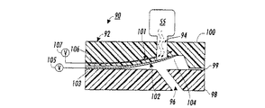
本発明の一実施形態に従うバルブ90の側断面図を図1に示す。バルブ90には、バルブハウジング92が含まれ、これは、流体の入り口または出口となるポート94と開口96を規定する。例示する実施形態においては、ポート94は、加圧空気を選択的に閉鎖できる入り口ポートとして最適に構成され、一方、開口96は、空気出口として構成される。しかし、最適動作に必要であれば、入り口と出口を交換または配置変更できることは、当業者には明らかである。
【0008】
バルブハウジング92は、開口板98(開口96を規定する)と、開口板98と間隔を空け平行に配置される対向ポート板100から形成される。ポート板100は、曲面101を持つ。例示する実施形態においては、板98と板100は、別の層として独立に形成され、後で接着層99により接合される。しかし、もちろん、ミクロ機械加工、プラスチック蒸着(plastic deposition)、その他の技術を使用し一体構造に形成することもできる。
【0009】
可撓性薄膜102は、板98と板100の間に挟み込まれる。示すように、薄膜102は、固定薄膜端103を持ち、これは、板98と板100の間に固定され、一方、固定されない薄膜端104は、板98と板100の間を自由に動く。
【0010】
可撓性薄膜102は、少なくとも一部は導電性とし、これに電圧を加え、ポート94が閉鎖されるポート閉鎖位置と、ポート94が閉鎖されないポート開放位置、またはこの逆、の間で、可撓性薄膜を正確にスイッチする。電極106は、板100の電極電圧電源107に取り付けられ、その上に誘電体層97が形成される。もちろん、可撓性薄膜102の一部として、可撓性誘電体層を組み入れることもできる。電極はスイッチ電極であり、電圧電源107から薄膜102と電極106の間にスイッチ電圧を加えると、固定されない薄膜端104を板100の方向に引きつける。薄膜電圧電源105は、固定薄膜端103に取り付けられ、バルブがアドレス可能なアレイの一部であるとき使用される。
【0011】
図2は、図1に示すバルブの平面図である。バルブのポート94と開口96の相対位置は、互いにずらして示すが、しかし、要求される任意の位置に配置することができる。この図において、薄膜102にオプションの開口95を判りやすく示している。開口95により、薄膜の弾性硬度が低減され、薄膜の運動と、薄膜が電極106に押圧/剥離されることの双方により生起される空気抵抗が低減される。薄膜の固体領域は、例えばパターン蒸着またはメッキにより穴と共に形成される。この替わりに、薄膜の形成後、例えば写真製版または打ち抜き加工により穴を形成することもできる。空気流に対するインピーダンスを比較的低く保つため、好ましい穴の直径は、ポート94の直径の約1/10とされる。図6に関連し以下で説明するように、バルブがパッシブマトリックス方式のアレイとして組み入れられる場合は、列アドレス線108と行アドレス線109が使用される。列アドレス線108は、薄膜電圧電源105に対応し、可撓性薄膜に取り付けられ、行アドレス線109は、電極電圧電源107に対応する。
【0012】
バルブ90は、多くの機械加工技術またはミクロ機械加工技術により形成され、これには、従来の集積回路製作またはプリント回路ボード製作に対応するものが含まれる。例えば、化学エッチング、電子ビーム製版、写真製版、その他標準の集積回路バッチ処理技術を使用し、必要な空気通路、制御用すなわち回路の通路、穴、オリフィス、開口を形成することができる。この替わりに、射出成形、高精密数値制御機械、立体製版を低コストのバルブバッチ形成に採用することもできる。この形成に使用される材料には、プラスチック、金属、ガラス、セラミックが含まれる。可能な一実施形態においては、プラスチック、エポキシ、ガラス、シリコン、ポリシリコン、窒化ケイ素、酸化ケイ素、オキシナイトライド(oxynitride)、プラスチックまたはアルミニウム、その他製版処理に適する可能な材料が、必要なバルブハウジング、バルブ機構、通路の形成に使用される。電極は、任意の導電性金属または導電性ポリマーから形成され、可撓性条片は、プラスチック薄膜、アルミニウム被覆のマイラー、メッキされたニッケル、ポリイミドが挟まれたアルミニウムから形成される。典型的な用途においては、各バルブのハウジングは、100立方mmの容積(10×10×1mm)より小さく、バルブハウジングの可撓性条片は、一般に、幅0.1〜10mm、長さ0.5〜50mm、厚さ1〜100μm程度の寸法を持つ。バルブの大きなアレイを形成することができ、メートル規模のアレイには、数万におよぶ個別バルブが含まれる。
【0013】
図1〜図3に示す片持ちバルブを製作する特定の処理には、開口基板(プラスチック、ガラス、FR4、等)の形成、例えば、開口アレイを含めるための射出成形、金属皮膜の付着または無電解メッキとこれに続く列アドレス線と片持ち薄膜のパターン形成が含まれる。図2に関連し説明したように、片持ち薄膜には、オプションとして穴が形成される。ポート基板も開口基板と同じ方法で製作される。金属を付着させパターンを形成し列アドレス線と電極を形成し、次いで、誘電体絶縁層、例えば電極の上にパリレンを付着させる。ポートの高さに比較し横構造の寸法が比較的大きいので、適当に大きな焦点深度の非平面写真製版パターンを形成することができる。基板または最上層のいずれかに接着層を付加し、開口基板とポート基板を揃え(光学的またはピンにより)、相互に圧着する。皮膜剥離層は取り除かれる。この後、オプションとして、水の吸収と浸透を軽減する疎水層を形成する処理を行うこともできる。
【0014】
図3、図4を参照すると、バルブ90の動作をよく説明できる。図3に見られるように、流体圧力源55はバルブに接続される。流体圧力源は、ファン、真空源、加圧された空気源、または使用される流体圧力の調整に適した任意の他の装置から提供される。流体圧力源が真空源の場合、図に示す特定のバルブ構成の開口96にそれを加える。図3の断面に見られるように、ポート94が薄膜102により閉鎖されていなければ、流体圧力源(一般には濾過された空気)は、バルブ90に入り、開口96を通り出る。電極106は電極電圧電源107に接続される。電圧107がスイッチ作動電圧まで増大されると、固定されない薄膜端104は、ポート板100の方向に動かされ、閉鎖位置に引きつけられる。薄膜の変位する部分と電極106が平行し近接することにより、容易に静電的な閉鎖が行われる。
【0015】
図4に示す閉鎖されないポート開放位置に薄膜を動かすため、電圧電源107は、固定されない薄膜端104をポート94に保持する電圧より低い電圧に下げられる。薄膜が、静電的に開放されると、ポート94が吹き開けられ、ポート開放状態になる。これにより、空気流は比較的大きな容量となり、バルブ通過高空気コンダクタンスを提供する。固定されない薄膜端の動きは、ポート94を通る加圧流体(空気)により付勢される。
【0016】
本発明の範囲には、別の薄膜構造と設計も含められる。例えば、図5に、同等部品には同一番号を付け、図1〜図4のバルブに類似するバルブ90’を示す。しかし、図5のポート板100’は、緩やかに曲がるポート板内面101ではなく、比較的平らで、直線のポート板内面101’を持つ。これによれば、平面薄膜の製作が容易である。誘電体層は、可撓性薄膜102’の上に形成される。誘電体層は、薄膜と電極の間の短絡を防ぐためのもので、電極106’と接触する可撓性薄膜の部分のみに形成すればよい。
【0017】
図5に示す片持ちバルブを製作する一つの処理には、開口基板(プラスチック、ガラス、FR4、等)の形成、例えば、開口アレイを含めるための射出成形、厚いキャストポリマー層による開口基板の充填とポリマー層の平面形成、金属皮膜の付着または無電解メッキと、これに続く列アドレス線とオプションの開口を持つ片持ち薄膜のパターン形成が含まれる。次いで、キャストポリマーが、見切りで取り除かれる。次いで、実施形態に示すように、誘電体層、例えばパリレンが片持ち薄膜に整合され付着される。ポート基板も開口基板と同じ方法で製作される。金属を付着させパターンを形成し電極を形成し、次いで、オプションとして追加される誘電体絶縁層(図示されない)を付着させる。基板または最上層のいずれかに接着層を付加し、開口基板とポート基板を揃え(光学的またはピンにより)、相互に圧着する。
【0018】
図6を参照すると、本発明の前述の実施形態に従う構造を持つバルブアレイのパッシブマトリクスアドレス指定によるスイッチ動作がよく示される。図6に、4バルブアレイ400の概略を示す。4個の片持ち薄膜バルブ410、420、430、440が、電圧アドレス線により制御される。各バルブは、同一構造であり、電極板(電極板411、421、431、441)を持つ。スイッチ作動前の開始位置(非閉鎖)にある片持ち薄膜(薄膜413、423、433、443)を点線で示し、一方、スイッチ作動後の位置を実線で示す(薄膜414、424、434、444)。アドレス線402は、板411、431に接続され、アドレス線404は、板421、441に接続され、アドレス線406は、片持ち薄膜413、423に接続され、アドレス線408は、片持ち薄膜433、443に接続される。
【0019】
図6に、バルブ410をスイッチし(ポート閉鎖位置に閉鎖)、同時に、残りのバルブ420、430、440をスイッチしない(開放)手順を示す。通常、全ての行(列)アドレス線は、持続電圧範囲にある同一電圧(この場合75(25)V)に維持され、従って、可動薄膜と板の間の電圧差は、開放されたバルブをスイッチするには小さ過ぎ、閉鎖されたバルブを開放するには大き過ぎる。バルブ410をスイッチするため、行アドレス線406の電圧が75Vから100Vに上げられ、列アドレス線402の電圧は25Vから0Vに下げられる。これは、電圧変化が全くないバルブ440の薄膜の最終位置444は変えない。バルブ420の薄膜の最終位置424も変更されない。薄膜電圧が先の75Vから100Vに上げられても、板421の電圧は依然として25Vであり、電圧差(75V)はスイッチ作動しきい値より小さく、静電スイッチを作動するには十分でない。同様に、板431と片持ち薄膜434の間の電圧差の大きさは75Vしかないので、バルブ430は、スイッチされないままである。しかし、特定のアドレスされたバルブ410はスイッチされる。バルブ410において、新しい電圧は100Vであり、薄膜をスイッチし、413の中立位置から新しい位置414に動かすのに十分である。同様にして、最初に閉鎖されている全てのバルブが開放される。多くの代替する電圧レベルが可能であり、電圧差がスイッチに適当であれば、例えば交流の電圧レベルを使用できることは、当業者には明らかである。ここに示す例は拡張することができ、簡単な電圧アドレス指定により、大きなバルブアレイの任意のバルブ素子をパッシブマトリクスアドレス指定することができる。
【0020】
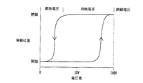
図7に、電圧を変え電極と薄膜の間に加えたときの、可撓性薄膜102の位置を示す。80〜90Vの間において、バルブは開放から閉鎖にスイッチされ、100V差において、薄膜位置は閉鎖位置にある。
【0021】
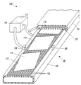
図6に関連し教示された加圧空気噴射を制御するバルブアレイが、紙のような可撓性対象が含まれる対象の操作に使用される。例えば、図8に、直接物理的に接触する必要なく、一枚の紙112を含む対象を操作するために最適化された処理システム110を一部示す。処理システム110は、コンベヤ120を持ち、これは、下部122と上部124に分割される。判りやすくするため、上部124を切り取り、紙の動きを示すが、上部124と下部122は、ほぼ同一の長さであることを理解する必要がある。部分122と部分124は、その間に通路123を規定するよう間隔が空けられ保持される。この通路は、紙112が接触しないで通過する大きさに設定される。部分122と部分124のそれぞれは、複数の独立にまたは準独立に制御される調整可能な空気噴射126を持ち、システム110を通過する紙112を動的に支持、移動、誘導する。図1〜図6のバルブの実施形態を参照し示すように、これら空気噴射126のいくつかは、本発明に従うバルブにより制御される。
【0022】
部分122と部分124に、対向する空気噴射を持つことにより、紙112の対向する側に空気流を調整可能に加え(空気噴射を向けることにより)、部分122と部分124の間に紙を動的に保持することができ、同時に、垂直、横、縦の力を加えることにより(これも、空気噴射を向けることにより)、紙の位置、速度、方向を正確に制御できる。さらに、追加の利点として、独立または準独立に制御される調整可能な空気噴射126を使用することにより、紙112の一部に向かう空気流を動的に増加または減少でき、紙の形状を、延ばし、平坦にし、曲げ、曲げの除去、その他要求される補正を行うことができ、同様に、紙の位置、方向、速度を調整できる。加えて、空気噴射126により加える空気流を適当に補正することにより、多様な重さ、寸法、機械的特性の紙を、容易に支持、加速することができる。例えば、重く、厚く、比較的可撓性の小さい厚紙類は、支持および誘導するため、噴射126から多くの空気流が必要であり、一方、軽量の紙シートは、全体としての空気流は少なくてよいが、フラッタ、または縁反り現象を補償するため、独立または準独立の空気噴射126により行う速くて頻繁な空気流の調整が必要である。
【0023】
可撓性対象のフラッタその他の動的な問題を補正するための可撓性対象の能動的な誘導(紙112の)は、少なくとも1つのセンシングユニット140を設けることにより可能となる。センシングユニット140は、紙112の動作状態を検知し、空間的動的情報(例えば光学画像形成システムまたは縁検出システムの用例において得られるような)を、動作解析システム150に与える。この動作解析システム150は、受信した情報から紙112の相対的または絶対的な動きを計算でき、この動作計算は、全体としての紙112の位置、方向、速度、同様に、紙112の小領域(紙112のたわみによる)の位置、方向、速度を与えるものである。一般に、動作解析ユニット150は、汎用コンピュータまたは専用ハードウェアシステムであり、対象の動きを求めるために必要な高速画像計算処理ができるものである。この計算された動作情報を使用し、動作解析ユニット150に接続される動作制御ユニット152が、制御信号をコンベア120に送り、紙112の小領域に向ける空気噴射の印加を選択的に増加または減少させることにより、紙112の動きを適当に補正し、フラッタ、座屈、巻き上がり、その他要求される運動状態からの望ましくない偏倚を減少させる。理解されるように、集積された動作解析と動作制御の組立体が考えられるので、独立のセンサ、動作解析ユニット、動作制御ユニットは必要でない。実際には、コンベヤ上に集積されるマイクロコントローラ組立体として、複数の集積されたセンサ、動作解析ユニット、動作制御ユニットを提供することができる。
【0024】
センシングユニット140がマイクロコントローラと独立または一体かの如何に関わらず、対象位置を適切に確定するため、センシングユニット140は、信頼性があり、正確であり、可撓性対象の比較的小さい領域を追跡するに十分な空間的、時間的解像度を持つ必要がある(一般的には少なくともこの領域は約1平方cmであり、しかし、もちろん、これより高いまたは低い解像度も使用できる)。さらに、多くの処理において対象は高速に動き、測定の追跡に100msより小さい値しか許容されない。幸いなことに、光学センサ、ビデオ画像形成システム、赤外線または光学縁検出器、その他特定の従来の検出器が、適当な空間的、時間的解像度を提供することができる。二次元光学センサ(例えば電荷結合素子(CCD's))、走査式一次元アレイ、連続位置検知検出器が使用され、よい結果が得られる。しかし、固定一次元センサアレイも使用される。理解されるように、光学センサではなく無接点センサも使用される。無接点センサには、これに限定されるものではないが、圧力センサ、音響センサ、静電センサが含まれる。
【0025】
動作においては、対象の動きをフィードバック制御するセンシングユニット140を使用することにより、対象の動作状態を精密に微細操作できる。例として図8に、コンベヤ120に沿う3つの異なる位置に、紙112を連続に示す。それぞれ、紙位置114、紙位置116、紙位置118の標識を付ける。位置114において、コンベヤ120に到達した紙112は向きがずれている。紙112が、空気噴射126により、コンベヤ120に沿い位置116に動かされると、センサ140は、紙112の瞬間ごとの位置に対応する不連続な空間的測定値を時間順に出力する。これらの空間的測定情報の時間順の要素は、動作解析ユニット150に連続的に渡される。動作解析ユニット150は、受け取った情報(センサが測定した一次元、二次元、三次元空間情報)を使用し、位置、速度、運動を含む、紙112の運動状態を正確に確定する。この情報(集約し“軌跡”と名付ける)は、動作制御ユニット152に渡され、これは、軌跡における誤差を最小にする補正応答を計算し、選択された空気噴射126に信号を送り、ずれを補正する。紙112は、位置116に示されるように正規位置に近付けられる。紙の軌跡にフィードバック制御の補正を行い、紙の向きを適当にフィードバック制御する処理を繰り返し、紙112の軌跡(紙112は、ここでは空間的に位置116に配置されている)を、最終的に位置118に示すように正確に揃える。理解されるように、可撓性対象の軌跡を補正するフィードバック制御処理は、ミリ秒のサイクルタイムで高速に繰り返される。これは、高速のセンサ、移動処理、空気噴射システムを採用すれば可能である。
【0026】
本発明に使用するのに適した一般的な空気噴射アーキテクチャを、図9に参照し示す。可撓性対象のコンベヤ320の一部には、可撓性対象(判りやすくするため可撓性対象は示さない)を横、縦、垂直に搬送する多様な空気噴射326が含まれる。空気噴射326には、コンベヤ面311に形成され、流れる空気360の出口または入り口となる溝354が含まれる。例えば、本発明に従う単一片持ち薄膜形式バルブ350(バルブの二次元アレイの一部)が、パッシブマトリクスアドレス指定により選択的に作動され、空間370の高圧空気が上方に流れ、可撓性対象に運動量を伝達し、下方にバルブ352を通過し、空間372に入る。
【0027】
図8に示すように、空間372は、仕切り371により空間370から分離され、空間372は、空間370より低い空気圧に維持される。
【0028】
可撓性対象の経路の制御は、複数の集積されたセンサ340を設けることにより行われる。このセンサ340には、これに制限するものではないが、光学、機械式、熱、静電、音響のセンサが含まれる。センサ340は、対象位置に関連するほぼ連続のセンサフィードバックを提供し、これにより、空気噴射326の近くを通過する可撓性対象の動きをほぼ連続的に制御する。理解されるように、センサ340から受ける情報は、図8に関連し説明した集中された動作解析ユニットと動作制御ユニットに渡される。替わりに、分散すなわちローカルの動作解析と動作制御を採用することもできる。例えば、センサ入力を解析し空気噴射の制御を指示するコンピュータマイクロ回路にセンサ340を組み込むことができる。
【0029】
図10は、可撓性対象コンベヤ220の側面図である。このコンベヤ220は、下部222と上部224に分割され、その間に通路223を持ち、各部分222と224は、複数の独立または準独立に制御される調整可能な空気噴射を持ち、システムを通過する紙212を、動的に支持、移動、誘導する。図8に関連し説明したように、部分222と部分224は対向する空気噴射を持ち、紙212の対向する側に調整可能な空気流を与え(空気流を向けることにより)、部分222と部分224の間に動的に紙を保持し、同時に、垂直、横、縦の力を加えることにより(これも空気噴射を向けることにより)、紙の位置、速度、方向を微細に制御する。例えば、紙212の縦の搬送は、それぞれ部分222と部分224に相互に対向し配置される空気噴射230と232を組み合わせ作動させることにより行われる。空気流260は、バルブ250とバルブ252により制御され、空気流は、縦方向の運動量を紙212に伝達する。紙212の位置を制御する別の例として、対向する空気噴射240と242を使用し、垂直に空気260を向け、コンベヤ220において要求される位置に紙212を浮遊させる。さらにこの機能は拡張することができ、一枚の紙の小領域に差分的な横または縦の張力を与え、曲がりの除去、巻き上げ、フラッタの除去、その他望ましい整紙機能を与える。
【図面の簡単な説明】
【図1】 開口閉鎖位置から開口非閉鎖位置に動く薄膜を示す本発明に従うバルブの側断面図である。
【図2】 上部開口板を取り除き、ポートに対する薄膜の位置を判りやすく示す図1のバルブの平面図である。
【図3】 開口閉鎖位置にある薄膜を示す図1と図2のバルブの側断面図である。
【図4】 開口非閉鎖位置にある薄膜を示す図1と図2のバルブの側断面図である。
【図5】 バルブの別の実施形態を示す側断面図である。
【図6】 1つのバルブがスイッチされ、残りのバルブがスイッチされていない状態の4つのバルブ位置の電圧アドレス指定を示す略図である。
【図7】 電圧差の変化に対する可撓性薄膜の位置を示す図である。
【図8】 紙の検出に使用されるセンサユニットと、センサユニットに接続され、適当な補正入力を空気噴射に与え、要求される経路、速度、方向に紙を保持する運動制御ユニットを持ち、本発明に従う可変流量バルブを使用し、空気噴射で支持される紙を正確高速に動かす紙操作システムを示す図である。
【図9】 バルブ制御される垂直、横、縦の空気噴射を持つ方向付き空気噴射システムと、可撓性対象の三次元の位置を正確にフィードバック制御する集積されたセンサシステムをあわせて示す図である。
【図10】 方向付けされる空気の流れのパターンを示す、図10に示すものに類似する有向空気システムの断面図である。
【符号の説明】
55 流体圧力源、90,90’ バルブ、92 バルブハウジング、94 ポート、95 オプションの開口、96 開口 、97 誘電体層、98 開口板、100 100’ 対向ポート板、101 曲面 内面、101’ 内面、102 102’ 可撓性薄膜、103 固定薄膜端、104 固定されない薄膜端、105 薄膜電圧電源、106 106’ 電極、107 電極電圧電源、108 列アドレス線、109 行アドレス線、110 処理システム、112 紙、114 116 118 紙位置、120 コンベヤ、122 下部、123 通路、124 上部、126 空気噴射、140 センサ、150 動作解析ユニット、152 動作制御ユニット、212 紙、220 コンベヤ、222 下部、223 通路、224 上部、230 232 空気噴射、240 242 空気噴射、250 252 バルブ、260 空気流、311 コンベヤ面、320 コンベヤ、326 空気噴射、340 センサ、354 溝、360 空気流、370 空間、371 仕切り、372 空間、400 4バルブアレイ、402 404 列アドレス線、406 408 行アドレス線、410 420 430 440 片持ち薄膜バルブ、411 421 431 441 電極板、413 423 433 443 薄膜の開始位置、414 424 434 444 薄膜の最終位置。[0001]
BACKGROUND OF THE INVENTION
The present invention relates to a cantilever valve that is electronically addressable and suitable for fluid flow control. In particular, the present invention relates to an addressable valve array that is particularly useful for applications that control the operation of air jets and manipulate paper.
[0002]
[Problems to be solved by the invention]
There are various applications for the technology to electrically control fluid at high speed using a group of inexpensive valve arrays, but it is difficult to economically manufacture a large two-dimensional valve array with the required tolerances. In addition, it is often difficult to accurately address and open and close valves in milliseconds.
[0003]
[Means for Solving the Problems]
The present invention provides an advanced valve. The valve is configured in a two-dimensional valve array, providing millisecond response time, high throughput collective array, and large pressure differential flow control. In addition, each valve in the array passive Or Active Matrix method Can be controlled by addressing. In a preferred embodiment, each valve includes a valve housing, which has an opening. Have The aperture plate is spaced from the aperture plate. Have a port Has an opposing plate. The first end of the flexible conductive thin film or strip is attached to the aperture plate or counterplate, and the second end is free to move between the plates. At least one switch electrode is used and the valve is activated. This switch electrode is a flexible thin film port Open position and port Move between closed positions. The dielectric layer between the flexible conductive thin film and the switch electrode prevents short circuit.
[0007]
DETAILED DESCRIPTION OF THE INVENTION
A side cross-sectional view of a
[0008]
The
[0009]
The flexible
[0010]
The
[0011]
FIG. 2 is a plan view of the valve shown in FIG. The relative positions of the
[0012]
Valve 90 is formed by a number of machining or micromachining techniques, including those corresponding to conventional integrated circuit fabrication or printed circuit board fabrication. For example, chemical etching, electron beam engraving, photoengraving, and other standard integrated circuit batch processing techniques can be used to form the required air passages, control or circuit passages, holes, orifices, openings. Alternatively, injection molding, high-precision numerical control machines, and three-dimensional plate making can be adopted for low-cost valve batch formation. Materials used for this formation include plastic, metal, glass and ceramic. In one possible embodiment, plastic, epoxy, glass, silicon, polysilicon, silicon nitride, silicon oxide, oxynitride, plastic or aluminum, or other possible materials suitable for plate making processes require a valve housing. Used to form valve mechanisms and passages. The electrode is formed from any conductive metal or conductive polymer, and the flexible strip is formed from a plastic thin film, aluminum coated mylar, plated nickel, aluminum sandwiched with polyimide. In a typical application, the housing of each valve is smaller than a volume of 100 cubic mm (10 × 10 × 1 mm), and the flexible strips of the valve housing are generally 0.1-10 mm wide and 0 length long. It has dimensions of about 5 to 50 mm and a thickness of about 1 to 100 μm. Large arrays of valves can be formed, and metric arrays include tens of thousands of individual valves.
[0013]
The specific process for fabricating the cantilevered valve shown in FIGS. 1-3 includes the formation of an aperture substrate (plastic, glass, FR4, etc.), for example, injection molding to include an aperture array, deposition of a metal coating, or no Electrolytic plating followed by column address line and cantilever patterning is included. As described in connection with FIG. 2, the cantilevered film is optionally formed with holes. The port substrate is also manufactured in the same way as the aperture substrate. Metal is deposited to form a pattern to form column address lines and electrodes, and then parylene is deposited over a dielectric insulating layer, such as an electrode. Since the dimensions of the lateral structure are relatively large compared to the height of the port, it is possible to form a non-planar photoengraving pattern having a suitably large depth of focus. An adhesive layer is added to either the substrate or the top layer, and the aperture substrate and port substrate are aligned (optically or by pins) and crimped together. The film release layer is removed. Thereafter, as an option, a treatment for forming a hydrophobic layer for reducing water absorption and permeation can be performed.
[0014]
3 and 4, the operation of the
[0015]
Not closed as shown in FIG. Port open In order to move the membrane to position, the
[0016]
Other thin film structures and designs are also within the scope of the present invention. For example, FIG. 5 shows a
[0017]
One process for making the cantilever valve shown in FIG. 5 includes forming an aperture substrate (plastic, glass, FR4, etc.), eg, injection molding to include an aperture array, filling the aperture substrate with a thick cast polymer layer. And planar formation of polymer layers, metal film deposition or electroless plating, followed by patterning of cantilevered films with column address lines and optional openings. The cast polymer is then removed by parting. Then, as shown in the embodiment, a dielectric layer, such as parylene, is aligned and deposited on the cantilevered film. The port substrate is also manufactured in the same way as the aperture substrate. A metal is deposited to form a pattern to form an electrode, and then an optional additional dielectric insulation layer (not shown) is deposited. An adhesive layer is added to either the substrate or the top layer, and the aperture substrate and port substrate are aligned (optically or by pins) and crimped together.
[0018]
Referring to FIG. 6, a valve array having a structure according to the above-described embodiment of the present invention. passive The switch operation with matrix addressing is well shown. FIG. 6 shows an outline of the 4-
[0019]
In FIG. 6, the
[0020]
FIG. 7 shows the position of the flexible
[0021]
The valve array that controls the pressurized air injection taught in connection with FIG. 6 is used to manipulate objects that include flexible objects such as paper. For example, FIG. 8 illustrates a portion of a
[0022]
Having opposing air jets in
[0023]
Active guidance (of the paper 112) of the flexible object to correct flutter and other dynamic problems of the flexible object is possible by providing at least one
[0024]
Whether or not the
[0025]
In operation, by using the
[0026]
A general air injection architecture suitable for use with the present invention is illustrated with reference to FIG. A portion of the
[0027]
As shown in FIG. 8, the
[0028]
Control of the path of the flexible object is performed by providing a plurality of
[0029]
FIG. 10 is a side view of the
[Brief description of the drawings]
FIG. 1 is a side cross-sectional view of a valve according to the present invention showing a membrane moving from an open closed position to an open non-closed position.
FIG. 2 is a plan view of the valve of FIG. 1 with the upper aperture plate removed and the position of the thin film relative to the port being easily understood.
FIG. 3 is a side cross-sectional view of the valve of FIGS. 1 and 2 showing the membrane in the open closed position.
4 is a side cross-sectional view of the valve of FIGS. 1 and 2 showing the membrane in the open non-closed position. FIG.
FIG. 5 is a side sectional view showing another embodiment of the valve.
FIG. 6 is a schematic diagram illustrating the voltage addressing of four valve positions with one valve switched and the remaining valves not switched.
FIG. 7 is a diagram showing the position of a flexible thin film with respect to a change in voltage difference.
FIG. 8 has a sensor unit used for paper detection and a motion control unit connected to the sensor unit, which gives an appropriate correction input to the air jet and holds the paper in the required path, speed and direction; It is a figure which shows the paper operation system which uses the variable flow valve according to this invention, and moves the paper supported by an air jet at high speed accurately.
FIG. 9 shows a directional air injection system with vertical, horizontal and vertical air injection controlled by a valve and an integrated sensor system that accurately feedback controls the three-dimensional position of a flexible object. It is.
FIG. 10 is a cross-sectional view of a directed air system similar to that shown in FIG. 10, showing the pattern of air flow directed.
[Explanation of symbols]
55 fluid pressure source, 90, 90 ′ valve, 92 valve housing, 94 port, 95 optional opening, 96 opening, 97 dielectric layer, 98 opening plate, 100 100 ′ counter port plate, 101 curved inner surface, 101 ′ inner surface, 102 102 'flexible thin film, 103 fixed thin film edge, 104 unfixed thin film edge, 105 thin film voltage power supply, 106 106' electrode, 107 electrode voltage power supply, 108 column address line, 109 row address line, 110 processing system, 112 paper 114 116 118 Paper position, 120 Conveyor, 122 Lower part, 123 Passage, 124 Upper part, 126 Air jet, 140 Sensor, 150 Motion analysis unit, 152 Motion control unit, 212 Paper, 220 Conveyor, 222 Lower part, 223 Passage, 224 Upper part , 230 232 Air injection, 240 242 Air , 250 252 Valve, 260 Air Flow, 311 Conveyor Surface, 320 Conveyor, 326 Air Injection, 340 Sensor, 354 Groove, 360 Air Flow, 370 Space, 371 Partition, 372 Space, 400 4 Valve Array, 402 404 Column Address Line , 406 408 row address line, 410 420 430 440 cantilever thin film valve, 411 421 431 441 electrode plate, 413 423 433 443 thin film starting position, 414 424 434 444 thin film final position.
Claims (4)
貫通する開口部を有すると共に前記開口部が開口する内面を有する開口板、および、前記開口板に対して間隔を空けて対向配置され、貫通するポートを有すると共に前記ポートが開口する内面を有するポート板を含むバルブハウジングと、
第1の端部が前記開口板と前記ポート板との間に取り付けられ、第2の端部が自由に移動自在な、導電性部分を有する可撓性薄膜と、
前記ポート板内面の近傍に配置され、前記可撓性薄膜を前記ポート板と前記開口板との間で縦方向に駆動することで前記可撓性薄膜の第2の端部を前記ポートを閉鎖する閉鎖位置と前記ポートを開放する開放位置との間で移動させるためのスイッチ電極と、
前記スイッチ電極と前記可撓性薄膜との間に配置される誘電体層と、を備え、
前記可撓性薄膜の第2の端部は、前記可撓性薄膜と前記スイッチ電極との間に形成される電位差による静電力によって前記ポートの閉鎖位置と前記ポートの開放位置との間を移動し、
前記可撓性薄膜の第2の端部が前記ポートの閉鎖位置へ移動するときの前記電位差は、前記可撓性薄膜の第2の端部が前記ポートの閉鎖位置から前記ポートの開放位置へ移動するときの電位差よりも大きいことを特徴とする片持ちバルブ。In a cantilever valve that controls fluid movement,
An opening plate having an opening that penetrates and having an inner surface through which the opening is opened, and a port that is disposed to face the opening plate with a space therebetween and has an inner surface through which the port opens. A valve housing including a plate;
A flexible thin film having a conductive portion with a first end attached between the aperture plate and the port plate and a second end freely movable;
Arranged near the inner surface of the port plate, the port is closed at the second end of the flexible thin film by driving the flexible thin film vertically between the port plate and the opening plate. A switch electrode for moving between a closed position to open and an open position to open the port;
A dielectric layer disposed between the switch electrode and the flexible thin film,
The second end of the flexible thin film is moved between the closed position of the port and the open position of the port by an electrostatic force generated by a potential difference formed between the flexible thin film and the switch electrode. And
The potential difference when the second end of the flexible membrane moves to the closed position of the port is such that the second end of the flexible membrane moves from the closed position of the port to the open position of the port. Cantilever valve characterized in that it is larger than the potential difference when moving.
前記流体を前記ポートに供給する流体圧力源をさらに備えることを特徴とする片持ちバルブ。The cantilever valve according to claim 1,
The cantilever valve further comprising a fluid pressure source for supplying the fluid to the port.
前記薄膜に流体抵抗を低減するための穴が形成され、
前記穴の直径は前記ポートの直径の約10分の1であり、前記穴は、前記ポートに接触する膜部分には穴がないように前記薄膜上に位置決めされていることを特徴とする片持ちバルブ。The cantilever valve according to claim 2,
A hole for reducing fluid resistance is formed in the thin film,
The diameter of the hole is about one tenth of the diameter of the port, and the hole is positioned on the thin film so that there is no hole in the membrane portion that contacts the port. Holding valve.
複数の開口部を有するとともに前記開口部が開口する内面を有する開口板、および、前記開口板に対して間隔を空けて対向配置され、複数のポートを有するとともに前記ポートが開口する内面を有するポート板を含む複数のバルブと、
それぞれが該複数のバルブのそれぞれに取り付けられた複数の導電性の可撓性膜であって、各可撓性膜がその第1の端部において前記開口板と前記ポート板の間に取り付けられ、第2の端部が移動自在であり、各可撓性膜が個別にアドレス指定可能であり、前記ポートを閉鎖する閉鎖位置と前記ポートを開放する開放位置との間で交互に切り替わる可撓性膜と、
前記複数のバルブの一部をアドレス指定により選択してスイッチ作動電圧と持続電圧のいずれかを印加するスイッチ電圧源と、
静電スイッチング力を作用させて前記複数の可撓性膜を前記ポートの閉鎖位置と前記ポートの開放位置との間で移動させるために各バルブにそれぞれ設けられ、前記スイッチ電圧源によって前記スイッチ作動電圧または持続電圧が印加される複数のスイッチ電極と、
前記スイッチ電極と前記可撓性膜との間に配置され、該可撓性膜とスイッチ電極との間の短絡を防ぐ複数の誘電体層と、を備え、
前記可撓性薄膜の第2の端部は、前記可撓性薄膜と前記スイッチ電極との間に形成される電位差による静電力によって前記ポートの閉鎖位置と前記ポートの開放位置との間を移動し、
前記可撓性薄膜の第2の端部が前記ポートの閉鎖位置へ移動するときの前記電位差は、前記可撓性薄膜の第2の端部が前記ポートの閉鎖位置から前記ポートの開放位置へ移動するときの電位差よりも大きい、ことを特徴とするバルブアレイ。A valve array that can be addressed in a passive matrix manner,
An opening plate having a plurality of openings and having an inner surface through which the opening is opened, and a port having a plurality of ports and an inner surface through which the ports are opened, spaced from the opening plate. A plurality of valves including a plate;
A plurality of conductive flexible membranes each attached to each of the plurality of valves, each flexible membrane being attached at a first end between the aperture plate and the port plate; Flexible membranes that are movable between two ends, each flexible membrane is individually addressable, and alternates between a closed position to close the port and an open position to open the port When,
A switch voltage source for selecting a part of the plurality of valves by addressing and applying either a switch operating voltage or a sustain voltage;
Each switch is provided to move the plurality of flexible membranes between a closed position of the port and an open position of the port by applying an electrostatic switching force, and the switch operation is performed by the switch voltage source. A plurality of switch electrodes to which a voltage or a sustained voltage is applied;
A plurality of dielectric layers disposed between the switch electrode and the flexible film to prevent a short circuit between the flexible film and the switch electrode,
The second end of the flexible thin film is moved between the closed position of the port and the open position of the port by an electrostatic force generated by a potential difference formed between the flexible thin film and the switch electrode. And
The potential difference when the second end of the flexible membrane moves to the closed position of the port is such that the second end of the flexible membrane moves from the closed position of the port to the open position of the port. A valve array characterized by being larger than the potential difference when moving.
Applications Claiming Priority (2)
| Application Number | Priority Date | Filing Date | Title |
|---|---|---|---|
| US09/004,639 US6032923A (en) | 1998-01-08 | 1998-01-08 | Fluid valves having cantilevered blocking films |
| US09/004,639 | 1998-01-08 |
Publications (2)
| Publication Number | Publication Date |
|---|---|
| JPH11270728A JPH11270728A (en) | 1999-10-05 |
| JP4262816B2 true JP4262816B2 (en) | 2009-05-13 |
Family
ID=21711748
Family Applications (1)
| Application Number | Title | Priority Date | Filing Date |
|---|---|---|---|
| JP2899A Expired - Lifetime JP4262816B2 (en) | 1998-01-08 | 1999-01-04 | Cantilever valves and valve arrays |
Country Status (2)
| Country | Link |
|---|---|
| US (2) | US6032923A (en) |
| JP (1) | JP4262816B2 (en) |
Families Citing this family (79)
| Publication number | Priority date | Publication date | Assignee | Title |
|---|---|---|---|---|
| US6345502B1 (en) * | 1997-11-12 | 2002-02-12 | California Institute Of Technology | Micromachined parylene membrane valve and pump |
| US6397880B1 (en) * | 1998-05-08 | 2002-06-04 | Festo Ag & Co. | Microvalve battery |
| US6792754B2 (en) * | 1999-02-15 | 2004-09-21 | Silverbrook Research Pty Ltd | Integrated circuit device for fluid ejection |
| AUPP869099A0 (en) * | 1999-02-15 | 1999-03-11 | Silverbrook Research Pty Ltd | A method and apparatus(IJ46P1E) |
| US6705345B1 (en) * | 1999-11-08 | 2004-03-16 | The Trustees Of Boston University | Micro valve arrays for fluid flow control |
| US6578816B1 (en) * | 2000-04-14 | 2003-06-17 | International Business Machines Corporation | Active micromechanical air valve for pressure control and method for making same |
| US6590267B1 (en) * | 2000-09-14 | 2003-07-08 | Mcnc | Microelectromechanical flexible membrane electrostatic valve device and related fabrication methods |
| US6340149B1 (en) | 2000-11-27 | 2002-01-22 | Xerox Corporation | Tethered fluid valve apparatus |
| US6676106B2 (en) | 2000-12-28 | 2004-01-13 | Xerox Corporation | Flap structure for electrostatic or magnetic applications and method for making same |
| US7280014B2 (en) * | 2001-03-13 | 2007-10-09 | Rochester Institute Of Technology | Micro-electro-mechanical switch and a method of using and making thereof |
| AU2002303933A1 (en) * | 2001-05-31 | 2002-12-09 | Rochester Institute Of Technology | Fluidic valves, agitators, and pumps and methods thereof |
| DE20116898U1 (en) * | 2001-10-15 | 2002-01-17 | Festo Ag & Co | microvalve |
| US7211923B2 (en) * | 2001-10-26 | 2007-05-01 | Nth Tech Corporation | Rotational motion based, electrostatic power source and methods thereof |
| US7378775B2 (en) * | 2001-10-26 | 2008-05-27 | Nth Tech Corporation | Motion based, electrostatic power source and methods thereof |
| US6670071B2 (en) * | 2002-01-15 | 2003-12-30 | Quallion Llc | Electric storage battery construction and method of manufacture |
| US6821347B2 (en) * | 2002-07-08 | 2004-11-23 | Micron Technology, Inc. | Apparatus and method for depositing materials onto microelectronic workpieces |
| US6955725B2 (en) * | 2002-08-15 | 2005-10-18 | Micron Technology, Inc. | Reactors with isolated gas connectors and methods for depositing materials onto micro-device workpieces |
| US6884296B2 (en) * | 2002-08-23 | 2005-04-26 | Micron Technology, Inc. | Reactors having gas distributors and methods for depositing materials onto micro-device workpieces |
| US20040040502A1 (en) * | 2002-08-29 | 2004-03-04 | Micron Technology, Inc. | Micromachines for delivering precursors and gases for film deposition |
| US20040040503A1 (en) * | 2002-08-29 | 2004-03-04 | Micron Technology, Inc. | Micromachines for delivering precursors and gases for film deposition |
| TW590982B (en) * | 2002-09-27 | 2004-06-11 | Agnitio Science & Technology I | Micro-fluid driving device |
| WO2004031630A1 (en) * | 2002-10-04 | 2004-04-15 | Pbt (Ip) Limited | Gas valve with proportional output |
| US6807892B2 (en) * | 2002-12-30 | 2004-10-26 | Xerox Corporation | Pneumatic actuator with elastomeric membrane and low-power electrostatic flap valve arrangement |
| US6846151B2 (en) * | 2003-02-21 | 2005-01-25 | Lockhead Martin Corporation | Non-contact aerodynamic diverter/stacker insertion system |
| US7335396B2 (en) * | 2003-04-24 | 2008-02-26 | Micron Technology, Inc. | Methods for controlling mass flow rates and pressures in passageways coupled to reaction chambers and systems for depositing material onto microfeature workpieces in reaction chambers |
| US7344755B2 (en) * | 2003-08-21 | 2008-03-18 | Micron Technology, Inc. | Methods and apparatus for processing microfeature workpieces; methods for conditioning ALD reaction chambers |
| US7235138B2 (en) | 2003-08-21 | 2007-06-26 | Micron Technology, Inc. | Microfeature workpiece processing apparatus and methods for batch deposition of materials on microfeature workpieces |
| US7422635B2 (en) * | 2003-08-28 | 2008-09-09 | Micron Technology, Inc. | Methods and apparatus for processing microfeature workpieces, e.g., for depositing materials on microfeature workpieces |
| US7217582B2 (en) * | 2003-08-29 | 2007-05-15 | Rochester Institute Of Technology | Method for non-damaging charge injection and a system thereof |
| US7287328B2 (en) * | 2003-08-29 | 2007-10-30 | Rochester Institute Of Technology | Methods for distributed electrode injection |
| US7056806B2 (en) | 2003-09-17 | 2006-06-06 | Micron Technology, Inc. | Microfeature workpiece processing apparatus and methods for controlling deposition of materials on microfeature workpieces |
| US7282239B2 (en) * | 2003-09-18 | 2007-10-16 | Micron Technology, Inc. | Systems and methods for depositing material onto microfeature workpieces in reaction chambers |
| US7323231B2 (en) * | 2003-10-09 | 2008-01-29 | Micron Technology, Inc. | Apparatus and methods for plasma vapor deposition processes |
| US7581511B2 (en) * | 2003-10-10 | 2009-09-01 | Micron Technology, Inc. | Apparatus and methods for manufacturing microfeatures on workpieces using plasma vapor processes |
| US7647886B2 (en) * | 2003-10-15 | 2010-01-19 | Micron Technology, Inc. | Systems for depositing material onto workpieces in reaction chambers and methods for removing byproducts from reaction chambers |
| GB0327093D0 (en) * | 2003-11-21 | 2003-12-24 | Koninkl Philips Electronics Nv | Active matrix displays and other electronic devices having plastic substrates |
| FR2862629B1 (en) * | 2003-11-25 | 2006-02-17 | St Microelectronics Sa | COOLING DEVICE OF AN INTEGRATED CIRCUIT |
| US7258892B2 (en) * | 2003-12-10 | 2007-08-21 | Micron Technology, Inc. | Methods and systems for controlling temperature during microfeature workpiece processing, e.g., CVD deposition |
| US6988706B2 (en) * | 2003-12-17 | 2006-01-24 | General Electric Company | Piezoelectric microvalve |
| US7472432B2 (en) * | 2003-12-30 | 2009-01-06 | Letty Ann Owen | Bathtub insert “Take-Five” |
| US7906393B2 (en) * | 2004-01-28 | 2011-03-15 | Micron Technology, Inc. | Methods for forming small-scale capacitor structures |
| US8581308B2 (en) * | 2004-02-19 | 2013-11-12 | Rochester Institute Of Technology | High temperature embedded charge devices and methods thereof |
| US7584942B2 (en) * | 2004-03-31 | 2009-09-08 | Micron Technology, Inc. | Ampoules for producing a reaction gas and systems for depositing materials onto microfeature workpieces in reaction chambers |
| US20050249873A1 (en) * | 2004-05-05 | 2005-11-10 | Demetrius Sarigiannis | Apparatuses and methods for producing chemically reactive vapors used in manufacturing microelectronic devices |
| US8133554B2 (en) | 2004-05-06 | 2012-03-13 | Micron Technology, Inc. | Methods for depositing material onto microfeature workpieces in reaction chambers and systems for depositing materials onto microfeature workpieces |
| US7699932B2 (en) * | 2004-06-02 | 2010-04-20 | Micron Technology, Inc. | Reactors, systems and methods for depositing thin films onto microfeature workpieces |
| WO2006012510A1 (en) * | 2004-07-23 | 2006-02-02 | Afa Controls, Llc | Microvalve assemblies and related methods |
| US7338475B2 (en) * | 2004-12-17 | 2008-03-04 | Cardinal Health 303, Inc. | Electret enhanced automatic IV drip chamber shutoff |
| US7328882B2 (en) * | 2005-01-06 | 2008-02-12 | Honeywell International Inc. | Microfluidic modulating valve |
| US20060165873A1 (en) * | 2005-01-25 | 2006-07-27 | Micron Technology, Inc. | Plasma detection and associated systems and methods for controlling microfeature workpiece deposition processes |
| US20060237138A1 (en) * | 2005-04-26 | 2006-10-26 | Micron Technology, Inc. | Apparatuses and methods for supporting microelectronic devices during plasma-based fabrication processes |
| US7438030B1 (en) | 2005-08-26 | 2008-10-21 | The United States Of America As Represented By The Administrator Of The National Aeronautics And Space Administration | Actuator operated microvalves |
| US20070074731A1 (en) * | 2005-10-05 | 2007-04-05 | Nth Tech Corporation | Bio-implantable energy harvester systems and methods thereof |
| DE102005062554A1 (en) * | 2005-12-27 | 2007-07-05 | Robert Bosch Gmbh | Micro-mechanical component used in the semiconductor industry comprises a cap having a membrane for closing an access opening |
| US8556227B2 (en) * | 2009-07-20 | 2013-10-15 | Burkhard Buestgens | Temperature-compensated piezoelectric flexural transducer |
| FR2948928B1 (en) * | 2009-08-06 | 2012-02-24 | Commissariat Energie Atomique | MICROCAVITE STRUCTURE AND ENCAPSULATION STRUCTURE OF A MICROELECTRONIC DEVICE |
| US20110073788A1 (en) * | 2009-09-30 | 2011-03-31 | Marcus Michael A | Microvalve for control of compressed fluids |
| DE112011102296B4 (en) * | 2010-07-08 | 2019-02-21 | Murata Manufacturing Co., Ltd. | Electronic surface mount component |
| JP5773666B2 (en) * | 2011-01-31 | 2015-09-02 | 三菱重工印刷紙工機械株式会社 | Counter ejector and box making machine |
| US20130314587A1 (en) * | 2011-02-07 | 2013-11-28 | DigitalOptics Corporation MEMS | Multi-State Electrostatic Actuator and Digital Camera Therewith |
| BR112014010426A2 (en) | 2011-11-01 | 2017-04-18 | Altria Client Services Inc | apparatus and method for packing loose product |
| CN103487959B (en) * | 2013-10-15 | 2015-12-02 | 深圳市华星光电技术有限公司 | The transcription roller that vacuum adsorption force is adjustable and the thin-film bonding method with this transcription roller |
| JP6287089B2 (en) * | 2013-11-13 | 2018-03-07 | 村田機械株式会社 | Substrate floating device, substrate transfer device, and substrate transfer device |
| US9636262B2 (en) * | 2014-06-26 | 2017-05-02 | The Procter & Gamble Company | Method and apparatus for transferring a discrete substrate |
| US9670616B2 (en) | 2014-12-11 | 2017-06-06 | Georgia-Pacific Consumer Products Lp | Active web spreading and stabilization shower |
| US10288191B2 (en) * | 2015-12-23 | 2019-05-14 | University Of Louisville Research Foundation, Inc. | Bilayer microvalve arrays for pneumatic and fluidic applications |
| US20190142111A1 (en) * | 2017-11-10 | 2019-05-16 | Head Technology Gmbh | Liner for sports shoes |
| US11548261B2 (en) | 2018-10-24 | 2023-01-10 | Toyota Motor Engineering & Manufacturing North America, Inc. | Structure with selectively variable stiffness |
| US11067200B2 (en) | 2018-10-24 | 2021-07-20 | Toyota Motor Engineering & Manufacturing North America, Inc. | Self-healing microvalve |
| US11041576B2 (en) * | 2018-10-25 | 2021-06-22 | Toyota Motor Engineering & Manufacturing North America, Inc. | Actuator with static activated position |
| US10946535B2 (en) | 2018-10-25 | 2021-03-16 | Toyota Motor Engineering & Manufacturing North America, Inc. | Earthworm-like motion of soft bodied structure |
| US11088635B2 (en) | 2018-10-25 | 2021-08-10 | Toyota Motor Engineering & Manufacturing North America, Inc. | Actuator with sealable edge region |
| US11081975B2 (en) | 2018-10-25 | 2021-08-03 | Toyota Motor Engineering & Manufacturing North America, Inc. | Somersaulting motion of soft bodied structure |
| US11498270B2 (en) | 2018-11-21 | 2022-11-15 | Toyota Motor Engineering & Manufacturing North America, Inc. | Programmable matter |
| US11195506B2 (en) | 2018-12-03 | 2021-12-07 | Toyota Motor Engineering & Manufacturing North America, Inc. | Sound-modulating windows |
| US11066016B2 (en) | 2018-12-18 | 2021-07-20 | Toyota Motor Engineering & Manufacturing North America, Inc. | Adjusting vehicle mirrors |
| US11479308B2 (en) | 2019-01-09 | 2022-10-25 | Toyota Motor Engineering & Manufacturing North America, Inc. | Active vehicle interface for crosswind management |
| US11192469B2 (en) | 2019-01-30 | 2021-12-07 | Toyota Motor Engineering & Manufacturing North America, Inc. | Vehicle seat with morphing bolsters |
| US11473567B2 (en) | 2019-02-07 | 2022-10-18 | Toyota Motor Engineering & Manufacturing North America, Inc. | Programmable surface |
Family Cites Families (22)
| Publication number | Priority date | Publication date | Assignee | Title |
|---|---|---|---|---|
| US3243181A (en) * | 1963-12-23 | 1966-03-29 | Pitney Bowes Inc | Sheet handling device |
| US3422411A (en) * | 1965-07-21 | 1969-01-14 | Ex Cell O Corp | Pneumatic movement of data member |
| US3405977A (en) * | 1966-08-04 | 1968-10-15 | Sperry Rand Corp | All-fluid unit record accelerator |
| US3414331A (en) * | 1967-02-09 | 1968-12-03 | Rapistan Inc | Valve for air film conveyors |
| US3437335A (en) * | 1967-06-16 | 1969-04-08 | Sperry Rand Corp | Fluid document transporter |
| US3550964A (en) * | 1969-03-14 | 1970-12-29 | Us Army | Flueric transport system |
| US3918706A (en) * | 1974-06-24 | 1975-11-11 | Ibm | Pneumatic sheet transport and alignment mechanism |
| US4618292A (en) * | 1977-02-28 | 1986-10-21 | International Business Machines Corporation | Controls for semiconductor wafer orientor |
| DD222187A3 (en) * | 1982-03-22 | 1985-05-08 | Textima Veb K | METHOD AND DEVICE FOR POSITIONING TEXTILE FLUID IMAGES |
| US4493548A (en) * | 1982-03-26 | 1985-01-15 | Eastman Kodak Company | Apparatus for supporting flexible members |
| US4874273A (en) * | 1987-03-16 | 1989-10-17 | Hitachi, Ltd. | Apparatus for holding and/or conveying articles by fluid |
| JPH01214554A (en) * | 1988-02-22 | 1989-08-28 | Canon Inc | Sheet positioning device |
| JPH0243418A (en) * | 1988-08-03 | 1990-02-14 | Kubota Ltd | Attitude control device for front loader |
| GB8823815D0 (en) * | 1988-10-11 | 1988-11-16 | Molins Plc | Pneumatic web feeding |
| DE69213340T2 (en) * | 1991-05-30 | 1997-03-27 | Hitachi Ltd | Valve and its use in a device made of semiconductor material |
| GB2275903A (en) * | 1992-04-30 | 1994-09-14 | Brian Edwin Jones | Load sensing and conveying system |
| US5441597A (en) * | 1992-12-01 | 1995-08-15 | Honeywell Inc. | Microstructure gas valve control forming method |
| DE4308276C2 (en) * | 1993-03-16 | 1997-09-04 | Heidelberger Druckmasch Ag | Guide device for an arch |
| KR970003620A (en) * | 1995-06-20 | 1997-01-28 | 김주용 | Insulating film planarization method of semiconductor device |
| US5634636A (en) * | 1996-01-11 | 1997-06-03 | Xerox Corporation | Flexible object handling system using feedback controlled air jets |
| US5897097A (en) * | 1996-09-06 | 1999-04-27 | Xerox Corporation | Passively addressable fluid valves having S-shaped blocking films |
| FR2757999B1 (en) * | 1996-12-30 | 1999-01-29 | Commissariat Energie Atomique | SELF-ALIGNMENT PROCESS THAT CAN BE USED IN MICRO-ELECTRONICS AND APPLICATION TO THE REALIZATION OF A FOCUSING GRID FOR FLAT SCREEN WITH MICROPOINTS |
-
1998
- 1998-01-08 US US09/004,639 patent/US6032923A/en not_active Expired - Lifetime
-
1999
- 1999-01-04 JP JP2899A patent/JP4262816B2/en not_active Expired - Lifetime
-
2000
- 2000-01-11 US US09/481,234 patent/US6120002A/en not_active Expired - Lifetime
Also Published As
| Publication number | Publication date |
|---|---|
| JPH11270728A (en) | 1999-10-05 |
| US6120002A (en) | 2000-09-19 |
| US6032923A (en) | 2000-03-07 |
Similar Documents
| Publication | Publication Date | Title |
|---|---|---|
| JP4262816B2 (en) | Cantilever valves and valve arrays | |
| JP3923625B2 (en) | Conveyance system and fluid jet array support system for moving flexible objects | |
| US6089534A (en) | Fast variable flow microelectromechanical valves | |
| JP4065043B2 (en) | Bistable valve passively addressable row and column array, paper handling system and normally closed bistable valve | |
| US6123316A (en) | Conduit system for a valve array | |
| JPH10169826A (en) | Valve and valve array | |
| US5897097A (en) | Passively addressable fluid valves having S-shaped blocking films | |
| US7465023B2 (en) | Micro-electromechanical ink ejection mechanism with electro-magnetic actuation | |
| US6807892B2 (en) | Pneumatic actuator with elastomeric membrane and low-power electrostatic flap valve arrangement | |
| EP1332547B1 (en) | Electrostatic/pneumatic actuators for active surfaces | |
| US5634636A (en) | Flexible object handling system using feedback controlled air jets | |
| JPH10176768A (en) | Microdevice supporting system and array of microdevice | |
| JP4253455B2 (en) | Continuous ink jet print head and method for transferring ink drops | |
| US6454260B1 (en) | Air jet board device | |
| US6505922B2 (en) | Continuous ink jet printhead and method of rotating ink drops | |
| US20020100889A1 (en) | Method and apparatus for high-speed fluid flow control | |
| JP2001339965A (en) | Piezoelectric actuator |
Legal Events
| Date | Code | Title | Description |
|---|---|---|---|
| A521 | Request for written amendment filed |
Free format text: JAPANESE INTERMEDIATE CODE: A523 Effective date: 20051129 |
|
| A621 | Written request for application examination |
Free format text: JAPANESE INTERMEDIATE CODE: A621 Effective date: 20051129 |
|
| RD04 | Notification of resignation of power of attorney |
Free format text: JAPANESE INTERMEDIATE CODE: A7424 Effective date: 20051129 |
|
| A131 | Notification of reasons for refusal |
Free format text: JAPANESE INTERMEDIATE CODE: A131 Effective date: 20080527 |
|
| A521 | Request for written amendment filed |
Free format text: JAPANESE INTERMEDIATE CODE: A523 Effective date: 20080708 |
|
| A131 | Notification of reasons for refusal |
Free format text: JAPANESE INTERMEDIATE CODE: A131 Effective date: 20081118 |
|
| A521 | Request for written amendment filed |
Free format text: JAPANESE INTERMEDIATE CODE: A523 Effective date: 20081210 |
|
| TRDD | Decision of grant or rejection written | ||
| A01 | Written decision to grant a patent or to grant a registration (utility model) |
Free format text: JAPANESE INTERMEDIATE CODE: A01 Effective date: 20090113 |
|
| A01 | Written decision to grant a patent or to grant a registration (utility model) |
Free format text: JAPANESE INTERMEDIATE CODE: A01 |
|
| A61 | First payment of annual fees (during grant procedure) |
Free format text: JAPANESE INTERMEDIATE CODE: A61 Effective date: 20090210 |
|
| FPAY | Renewal fee payment (event date is renewal date of database) |
Free format text: PAYMENT UNTIL: 20120220 Year of fee payment: 3 |
|
| R150 | Certificate of patent or registration of utility model |
Free format text: JAPANESE INTERMEDIATE CODE: R150 |
|
| FPAY | Renewal fee payment (event date is renewal date of database) |
Free format text: PAYMENT UNTIL: 20120220 Year of fee payment: 3 |
|
| FPAY | Renewal fee payment (event date is renewal date of database) |
Free format text: PAYMENT UNTIL: 20130220 Year of fee payment: 4 |
|
| FPAY | Renewal fee payment (event date is renewal date of database) |
Free format text: PAYMENT UNTIL: 20140220 Year of fee payment: 5 |
|
| R250 | Receipt of annual fees |
Free format text: JAPANESE INTERMEDIATE CODE: R250 |
|
| R250 | Receipt of annual fees |
Free format text: JAPANESE INTERMEDIATE CODE: R250 |
|
| R250 | Receipt of annual fees |
Free format text: JAPANESE INTERMEDIATE CODE: R250 |
|
| R250 | Receipt of annual fees |
Free format text: JAPANESE INTERMEDIATE CODE: R250 |
|
| R250 | Receipt of annual fees |
Free format text: JAPANESE INTERMEDIATE CODE: R250 |
|
| EXPY | Cancellation because of completion of term |