JP4236830B2 - Storage device with upload function - Google Patents
Storage device with upload function Download PDFInfo
- Publication number
- JP4236830B2 JP4236830B2 JP2001207211A JP2001207211A JP4236830B2 JP 4236830 B2 JP4236830 B2 JP 4236830B2 JP 2001207211 A JP2001207211 A JP 2001207211A JP 2001207211 A JP2001207211 A JP 2001207211A JP 4236830 B2 JP4236830 B2 JP 4236830B2
- Authority
- JP
- Japan
- Prior art keywords
- software
- module
- external
- external device
- flash memory
- Prior art date
- Legal status (The legal status is an assumption and is not a legal conclusion. Google has not performed a legal analysis and makes no representation as to the accuracy of the status listed.)
- Expired - Fee Related
Links
- 238000012545 processing Methods 0.000 claims description 79
- 238000000034 method Methods 0.000 claims description 37
- 230000008569 process Effects 0.000 claims description 24
- 238000006243 chemical reaction Methods 0.000 claims description 15
- 230000004044 response Effects 0.000 claims description 11
- 230000005540 biological transmission Effects 0.000 claims description 8
- 230000006870 function Effects 0.000 description 61
- 238000010586 diagram Methods 0.000 description 18
- 230000000694 effects Effects 0.000 description 4
- 238000012546 transfer Methods 0.000 description 4
- 230000008859 change Effects 0.000 description 2
- 230000007246 mechanism Effects 0.000 description 2
- 238000004364 calculation method Methods 0.000 description 1
- 238000004891 communication Methods 0.000 description 1
- 230000000295 complement effect Effects 0.000 description 1
- 238000005516 engineering process Methods 0.000 description 1
- 230000002093 peripheral effect Effects 0.000 description 1
- 239000004065 semiconductor Substances 0.000 description 1
- 238000013519 translation Methods 0.000 description 1
Images


Landscapes
- Stored Programmes (AREA)
Description
【0001】
【発明の属する技術分野】
本発明はセキュリティ機能を搭載した記憶装置及びその記憶装置が挿入可能なホスト機器及びその記憶装置が挿入されたホスト機器に係り、フラッシュメモリチップ及びコントローラを有するメモリカード及びメモリカードが挿入可能な装置及びメモリカードが挿入された端末装置に関する。
【0002】
【従来の技術】
MultiMediaCard(「MultiMediaCard」はInfineonTechnologiesAGの登録商標である。以下「MMC」と称する)は、外部端子に電源供給端子、クロック入力端子、コマンド入出力端子、データ入出力端子、グランド端子、CS端子を含み、記憶素子からなるフラッシュメモリとこれを制御するマイコンチップを有する。MMCは外部端子から電源が供給されることで動作し、外部端子を通じて、外部端子と接続される外部機器(以下、「ホスト機器」と称する)、例えば携帯電話などとの間で電気信号を送受信することにより、フラッシュメモリのデータの読み書き及び転送モード、データの転送単位の変換等をおこなう。現在、MMCは、音楽データや画像データ等の保存及び読み出しをおこなうための小型ストレージとして利用されている。
【0003】
【発明が解決しようとする課題】
MMCにモジュールもしくはチップを追加することで新たな機能を持たせることができる。従来、MMCに追加された新たな機能をホスト機器が利用する際は、ホスト機器は、MMCの新しい機能に対応するソフトウエア(ドライバ)を別の装置等からダウンロードする必要があった。また、ホスト機器は、ホスト機器に接続されるMMCごとにMMCに対応するドライバを格納・設定する必要があり、ホストにおいて多くのメモリ容量を消費するという問題があった。さらに、ホスト機器を有するユーザがMMCを利用する際に特別な操作が必要なため利便性は低いという問題があった。また、MMCに新たに追加された機能が、機能として同一であっても、MMCへの実装の仕方の違いにより、またMMCの仕様のバージョンの違いにより、ホスト機器が異なるドライバを要する必要があるという問題があった。
【0004】
本発明の目的は、新たな機能を有するMMCを動作させるモジュールを提供することである。
【0005】
【課題を解決するための手段】
上記の目的を達成するために、本発明では、データを記憶する記憶装置であって、外部機器と接続される外部端子と、外部機器が記憶装置を使用する際に用いるドライバが格納されたフラッシュメモリと、記憶装置の動作を制御する制御部とを有し、制御部は、外部機器の指示に応じて、フラッシュメモリに格納されているドライバを読み出し、外部端子を介して外部機器に送信する構成とする。
【0006】
又、本発明の別の実施態様として、データを記憶する記憶装置であって、外部機器と接続される外部端子と、不揮発性の記憶媒体で構成されたフラッシュメモリと、記憶装置の動作を制御する制御部とを有し、制御部は、外部機器が記憶装置を使用する際に用いるソフトウエアが格納されているフラッシュメモリの領域を示す情報を有し、外部機器の指示に応じて、フラッシュメモリの領域に格納されているソフトウエアを情報を用いて読み出し、外部端子を介して外部機器に送信する構成としても良い。
【0007】
さらに、制御部は、データの暗号化及び復号化を行う暗号処理部を有する構成とすることができる。
【0008】
また、暗号処理部は、ICカードチップであってもよい。
【0009】
さらに、本発明においては、ソフトウエアが暗号化されており、制御部は、外部機器の指示に応じて前記ソフトウエアを読み出すときに、暗号処理部を用いてソフトウエアを復号化して外部機器に送信する構成とすることができる。
【0010】
また、本発明の別の実施態様として、データを記憶する記憶装置であって、外部機器と接続される外部端子と、不揮発性の記憶媒体で構成されたフラッシュメモリと、記憶装置の動作を制御する制御部と、データの暗号化及び復号化を行う暗号処理部とを有し、制御部は、外部機器が記憶装置を使用する際に用いるソフトウエアが格納されている前記フラッシュメモリの領域を示す情報を有し、外部機器の指示に応じて、フラッシュメモリの領域に格納されているソフトウエアを情報を用いて読み出し、暗号処理部を用いて復号し、外部端子を介して外部機器に送信するという構成としてもよい。
【0011】
【発明の実施の形態】
図1は、本発明を適用したMMCの内部構成を示す図である。MMC120は、MMC仕様に準拠するのが好ましい。MMC120は、MMC120と接続されたホスト機器100が発行するMMC仕様に準拠したメモリカードコマンドにしたがって、機密データ保護や個人認証などに必要な暗号演算をおこなうセキュリティ処理機能を有する。ホスト機器100は、例えば、携帯電話、携帯情報端末(PDA)、パーソナルコンピュータ、音楽再生(及び録音)装置、カメラ、ビデオカメラ、自動預金預払器、街角端末、決済端末等が該当する。
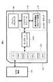
【0012】
MMC120は、MMC外部端子130、コントローラチップ150、及びフラッシュメモリチップ160を有する。MMC外部端子130は、ホスト機器100と接続される電源供給端子、クロック入力端子、コマンド入出力端子、データ入出力端子、グランド端子等を有する。フラッシュメモリチップ160は、不揮発性の半導体メモリを記憶媒体とするメモリチップであり、フラッシュメモリコマンドによりデータの読み書きがなされる。フラッシュメモリチップ160へのデータアクセスについてセキュリティ処理が伴う場合、そのセキュリティ処理は暗号処理機能付きメモリ装置170を介して行われる。
【0013】
コントローラチップ150は、アップロードモジュール140及び暗号処理機能付きメモリ装置170を有する。
【0014】
図12は、コントローラチップ150の構成を示す図である。MMCインターフェイス制御回路1210は、MMC外部端子130、アップロードモジュール140、及びコントローラモジュール1220と接続されており、MMC外部端子130の制御を行う。アップロードモジュール140は、MMC インターフェイス制御回路1210及びコントローラモジュール150と接続されている。アップロードモジュール140は、ホスト機器100とMMC120とが接続され、MMC120がホスト機器100から電源を供給される時に、ホスト機器100にプログラムをアップロードする機能を有する。アップロードされるプログラムは、インターフェイスドライバ、コマンド変換モジュール、及び並列化高速処理用ドライバ等が該当する。これらのプログラムは、MMC仕様と互換性のある外部端子を有し、かつMMC標準の仕様に基づくコマンド解釈機能又はフラッシュメモリアクセス機能又はモード変換機能等を有するホスト機器に対して、MMC内部に追加された機能の利用及びMMCの仕様変更等に適応するのに用いられる。
【0015】
アップロード作業を開始するアップロードモジュール140は、MMC インターフェイス制御回路1210と論理的に接続される。アップロードの作業終了後は、アップロードモジュール140とMMC インターフェイス制御回路1210との論理的接続は解除され、MMC インターフェイス 制御回路1210は、コントローラモジュール1220と論理的に接続される。この状態は、再び電源が入れられるまで有効である。コントローラモジュール1220は、アップロードモジュール140、MMC インターフェイス 制御回路1210、フラッシュメモリ制御回路1230、及び暗号処理機能付きメモリ装置インターフェイス制御回路1240と接続されており、これらを制御するモジュールである。暗号処理機能付きメモリ装置170は、暗号処理機能付きメモリ装置インターフェイス制御回路1240と接続されており、セキュリティ処理機能を備えたメモリ装置である。
【0016】
コントローラモジュール1220は、暗号処理機能付きメモリ装置インターフェイス制御回路1240に暗号処理用コマンドを発行することによって、ホスト機器100から要求されたセキュリティ処理に必要な演算の実行を暗号処理機能付きメモリ装置170に指示する。暗号処理機能付きメモリ装置170のインターフェイスの仕様がMMCの標準の仕様と異なる場合、ホスト機器100から送られてきたデータは、コントローラモジュール1220又は暗号処理機能付きメモリ装置インターフェイス制御回路1240が有する命令変換装置で変換されて暗号処理機能付きメモリ装置170へ送られる。
【0017】
図13は、暗号処理演算機能付きメモリ装置170の構成を示す図である。暗号処理演算機能付きメモリ装置170は、CPU1320、RAM1350、アプリケーション及びデータを格納するROM1330、及びEEPROM1440を有する。暗号演算の処理をおこなうためのコプロセッサ1360を有してもよい。これらの装置は内部バス1380で接続され、外部接続インターフェイス制御回路1370、及び外部接続インターフェイス1310を介して外部の機器と接続される。このような機能を有する暗号演算機能付きメモリ装置170としては、例えばICカードチップが該当する。ICカードチップは、外部機器を接続するためのシリアルインターフェイスを有する。シリアルインターフェースの電気的及び論理的仕様は、ISO7816において定められた仕様に準拠している。このようなホスト機器100より送られるMMCの標準命令と異なる命令を処理するモジュールは、演算機能付きメモリ装置1240に限らない。このような機器として、具体的には、暗号処理装置及びBluetooth端末モジュール等が該当する。暗号処理装置は暗号処理機能付きメモリ装置170からCPUを除き、複数の暗号処理命令を実行するための専用プロセッサを付加したものである。Bluetooth端末モジュールはBluetooth SIG(Special Interest Group)により標準化がなされている仕様に従ったモジュールである。
【0018】
MMC120は、MMC仕様に準拠した外部インターフェイスを有するのが好ましい。MMC120は、一種類の外部インターフェイスを通じて、標準メモリカードコマンド(フラッシュメモリチップ160へアクセスするためのコマンド)に加え、セキュリティ処理を実行するコマンドを受け付けることができる。コントローラチップ150は、MMC120の受信したコマンドが標準メモリカードコマンドであるか、セキュリティ処理を実行するコマンドであるかによって、アクセスすべきチップもしくはモジュールを選択し、コマンド処理を分配する機能を有する。標準メモリカードコマンドを受信したコントローラチップ150は、フラッシュメモリチップ160を選択し、これにフラッシュメモリコマンドを発行してホスト機器100とデータの読み書きをおこなう。また、セキュリティ処理を実行するコマンドを受信したコントローラチップ150は、暗号処理機能付きメモリ装置170を選択し、セキュリティ処理の実行を指示する。この時、受信したコマンドがICカードチップ170に適したフォーマットでない場合には、フォーマットの変換をおこなう。
【0019】
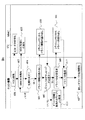
図2及び図3は、ホスト機器100へMMC120を挿入する際に行われる処理の流れを示すフローチャートである。
【0020】
まず、ホスト機器100は、MMC120を活性化するために電源供給を開始する(201)。電源供給が開始されたMMC120は、アップロードモジュール140を起動する(251)。起動されたアップロードモジュール140は、暗号処理機能付きメモリ装置170の初期化処理をおこない、ホスト機器100からCMD0が発行されるのを待つ(253)。CMD0はMMC標準メモリカードのコマンドの一つで、MMCをソフトウエアリセットするのに用い、MMCを初期化する際に発行されるコマンドである。
【0021】
ホスト機器100は、MMC120への電源供給開始後、MMC120に対してCMD0を発行する。このときホスト機器100は、MMC外部端子130のCSピンへ供給する信号をLOWにするかHIGHにするかによって、MMC120のモードを切り替える。CSピンがLOWの状態でCMD0が発行された場合、MMC120は、SPIモードとして初期化処理をおこなう(202)。MMC120は、CMD0を受け取るとCSピンの状態に基づいて、MMC120自身のモードを切り替える(252)。CSピンがLOWならば、SPIモードとして動作する(254)。CSピンがHIGHの場合、ホスト機器100は、MMC120の初期化を指示する(203)。ここでSPIはSerial Peripheral Interfaceの略である。MMCは通常、相対アドレスによりカードの選択をおこない、コマンド入出力端子でホスト機器からのコマンドの受信とレスポンスの送信を、データ入出力端子でデータの入出力をおこなう。これに対しSPIモードではCS端子をLOWにアサートすることでカードの選択を行い、MMCのコマンド入出力端子と同じ端子を用いるデータ入力端子でレスポンスとデータの送信を、MMCのデータ入出力端子と同じ端子を用いるデータ出力端子でコマンドとデータの受信をおこなう。またMMCとSPIモードはレスポンスのフォーマットや利用できるコマンドにおいても違いを持つ。ホスト機器100の指示を受けたアップロードモジュール140は、MMC120の初期化をおこなう。初期化処理が終了しなかった場合は初期化処理を繰り返し実行する(257)。初期化が成功した場合、アップロードモジュール140は、ホスト機器100からのコマンド受け待ち状態に入る(259)。
【0022】
ホスト機器100がアップロードモジュール140に対応していない場合(204)、ホスト機器100はMMC120の初期化を指示するコマンド、すなわちCMD0を発行する(205)。アップロードモジュール140は、CMD0を受け取ると(259)、アップロードモジュール140自身の動作を停止させ、MMC120は標準メモリカードコマンドに従いMMC120の動作を開始する(261)。この場合、ホスト機器100は、標準に搭載されたドライバを用いて動作する(207)。この初期化の手順は、ホスト機器100がアップロードモジュール140に対応していない場合に、MMC120を通常の標準コマンドフォーマットに従うMMCとして動作させたい場合に用いられる。
【0023】
ホスト機器100がアップロードモジュールに対応する端末なら(203)、ホスト機器100は初期化アプリケーションを起動する(209)。初期化アプリケーションは、MMC120に搭載されたドライバをダウンロード、もしくはホスト機器100内のライブラリに登録されたドライバを呼び出すため等の初期設定をおこなう。初期設定終了後、ホスト機器100は、MMC120に対しドライバ情報送信要求をおこなう(211)。MMC120は、コマンド受け待ち時にドライバ情報の要求を受け取ると(263)、フラッシュメモリ160よりドライバ情報を読み出し、ホスト機器100に送信する(351)。ホスト機器100は、MMC120から受け取ったドライバ情報の内容をホスト機器100に格納されたドライバ情報と照合し(301)、ドライバのダウンロードが必要かどうかを判断する(303)。この時、ホスト機器100は、ホスト機器100を使用するユーザにドライバのダウンロードをおこなうかどうかを確認してもよい。
【0024】
ドライバ情報には、ドライバ情報のサイズ、ドライバの種別、製造者名、登録日時、バージョンNo.、容量、プログラムの種類、対応端末、暗号化されている場合の鍵情報および対応するアプリケーション情報、ドライバデータのハッシュ値、シーケンスコマンドファイルのパス、及び格納場所へのパス等の情報が含まれている。ドライバ情報のサイズは、固定ビット長によって表されるドライバ情報のサイズである。ドライバの種別は、そのドライバが何のために用いられるかを示す。製造者名は、製造元の登録番号もしくは登録者を特定可能な文字列である。登録日時は、ドライバがカードに登録された日時を示す。バージョンNo.は、ドライバの改定番号を示す。容量は、ホストに要求されるドライバプログラムの容量を示す、プログラムの種類は、プログラムが配布される時の形式(バイナリコード、Javaアプレット、DLL、ソースプログラム等)を示す。対応端末は、対応するホスト機器のベンダー名(例えばNTT 503i シリーズ等)を示す。暗号化された場合の鍵情報及びアプリケーション情報は、ドライバが共通鍵もしくは秘密鍵等で暗号化されている場合に復号をおこなう暗号処理機能付きメモリ装置170に設定する鍵情報等が含まれたDF(Dedicated File)へのパス及び設定情報を指す。ドライバデータのハッシュ値は、ドライバのデータのハッシュを取った値である。ハッシュ値を計算するために用いるアルゴリズムとしては、SHA-1、MD5等が考えられる。シーケンスコマンドファイルのパスは、ドライバ読み出し手続きを記述したファイルで、オプショナルシーケンス等において図2及び図3とは異なるシーケンス処理を要求する場合にあらかじめ読み込んでおく。格納場所へのパスはURL(Uniform Resource Locator)でもよい。URLの場合、ホスト機器100は、インターネットを介してドライバのダウンロードをおこなう。
【0025】
ドライバ情報は、暗号処理機能付きメモリ装置170に格納されてもよい。この場合、アップロードモジュール140は、保存場所、及びファイルを開くためのPIN情報等を指定して、暗号処理機能付きメモリ装置170からドライバ情報の読み出しをおこなう。また、ドライバ情報に含まれるドライバの種類の数は複数個でも良く、含まれるデータは上記の種別に限られない。
【0026】
MMC120がドライバ情報を送った後、初期化アプリケーションはオプショナルシーケンスを実行しても良い(380)。オプショナルシーケンスは、ドライバ情報に含まれる暗号化された場合の鍵情報及びアプリケーション情報に基づき、暗号処理機能付きメモリ装置170を用いてフラッシュメモリチップ160に格納された暗号化されたドライバを認証及び復号し、ホスト機器100へ送信する場合に使用される。オプショナルシーケンスの開始と終了は、ホスト機器100がMMC120にREAD命令を送る際に、ドライバを指示するアドレスを送付するかどうかで決定される。ホスト機器100は、この段階でMMC120のセキュリティ機能を直接呼び出せない。この場合、ホスト機器100は、あるシーケンスな処理に基づいたWRITE命令とREAD命令をセキュリティ命令の代用として発行する。アップロードモジュール140は、ホスト機器100から発行されたWRITE命令及びREAD命令を処理手順に従って処理することで、セキュリティ命令と解釈して実行する。
【0027】
図14は、ドライバが暗号化されている場合のドライバ読み込み処理のフローチャートである。アップロードモジュール140は、フラッシュメモリチップ160よりドライバ情報を読み込み(1451)、ホスト機器100に送信する(1401)。ホスト機器100は、送信されたドライバ情報を元にドライバの保存場所のパスと復号のための鍵が保存されたファイルを認証するためのPINをWRITE命令で指定する(1403)。アップロードモジュール140は、ホスト機器100より送られてきた命令がWRITE命令であるか(1453)、パス及びPIN情報が正しいかどうかを判別し(1455)、正しいならばフラッシュメモリチップ160より暗号化されたドライバを読み出して復号を行う(1457)。パス及びPIN情報が正しくない場合、アップロードモジュール140は、エラー処理を実行してエラーをホスト機器100に通知する(1461)。エラー処理は、PINの認証失敗によるアクセス制限やWRITE−READシーケンスのリセット等が該当する。ホスト機器100は、ドライバが判読可能で正しいかどうかを判別し(1405)、正しい場合はドライバの登録ステップ309に移行する。正しくない場合、ホスト機器100は、再びドライバを指定しなおす。正しくない場合とは、ドライバが何らかの理由により書き変わっている場合、指定された鍵が正しくない場合、及びドライバが暗号化されていない場合等が該当する。これらの処理は、アップロードモジュール140の実装の仕方によって様々な手順が考えられるが、WRITE命令−READ命令の順で処理を行うことが望ましい。
【0028】
図3に戻って説明を続ける。
【0029】
ホスト機器100からドライバ送信要求が出されると(305)、アップロードモジュール140は、フラッシュメモリチップ160からドライバを読み出し(353)、ホスト機器100に送信する(355)。この時、ドライバは認証を通じてダウンロードされても良い。又、ドライバは種別、サイズ、ハッシュ値の情報を含んでも良い。次にホスト機器100は、ドライバの登録を行う(309)。その後、ホスト機器100は、ドライバのフォーマットに従った処理を開始する(313)。MMC120は、アップロードモジュール140の処理を終了する(357)。もし、ホスト機器100がドライバの登録に関して制限を設けているならば、ホスト機器100は、内部でその処理に適合した処理をおこなう。具体的には、ホスト機器100のサービスを提供するベンダーが認証したIDを有するアプリケーション(ドライバ)しかホスト機器100内で実行できない場合等が該当する。この場合、ホスト機器100は、ドライバの有する認証情報とホスト機器100内部又はインターネット上のサーバー等外部にある認証情報を用いて、このアプリケーション(ドライバ)が登録可能か判断をおこなう。
【0030】
図4は、ホスト機器100としてJava搭載の携帯端末を想定し、WAP(Wireless Application Protocol)のサービスをおこなう例を示した図である。
【0031】
ホスト機器100は、ホスト機器外部端子410 を介してMMC インターフェイスドライバ420を用いてMMC120と通信をおこなう。ここでMMC120はセキュリティ処理をおこなうWIM(WAP Identity Module)として動作する。WIMとは、ワイヤレス通信ネットワーク上でサービスをおこなうアプリケーションのために、WAP forumにおいて定められた仕様である。
【0032】
ホスト機器外部端子410は、MMC外部端子130と互換性のあるインターフェイスを有する。初期化アプリケーション430は、MMC インターフェイスドライバ420を介しMMC120とデータの送受信をおこなう機能を有する。初期化アプリケーション430は、アップロードモジュール140をサポートしていないMMC120と互換性を保ち、汎用のアップロードモジュールの処理手順で可能な範囲で、この初期化アプリケーション430とMMC インターフェイスドライバ420もしくはホスト外部端子410の間に初期設定ドライバを含んでもよい。初期設定ドライバには、コマンド変換ドライバ、インターフェイス変換ドライバ等が該当する。ホスト機器100がMMC120と互換性のないインターフェイス制御回路で動作している場合や、外部端子変換コネクターを用いて動作をおこなう場合等に上記機能を使用する。初期化アプリケーション430は単独で動作してもよく、他のアプリケーションの中に含まれてもよい。この場合、初期化アプリケーションはJava上で動作するアプレットであることが望ましい。初期化アプリケーション430は、WTLS470もしくはWAPアプリケーション460からWIM命令の送信もしくはWIM命令の応答を受信するためのドライバをMMC120から読み込む。この手順は前記の図2及び図3に述べたとおりである。
【0033】
アップロード作業終了後、ホスト機器100に含まれるアプリケーションは、ダウンロードされたドライバを用いてMMC120のセキュリティ処理を利用することが可能になる。この時ドライバがインターフェイスドライバを含むものであるなら、外部端子変換コネクターを利用することで任意の仕様の外部端子に対してこの仕組みを利用することができる。
【0034】
MMC120以外の外部端子の使用としては、SDメモリカード、及びメモリスティック(メモリスティックは、(株)ソニーの登録商標である)等が考えられる。SDメモリカードは、幅24ミリメートル、長さ32ミリメートル、厚さ2.1ミリメートルであり、9つの外部端子をもち、フラッシュメモリを搭載した小型メモリカードである。
【0035】
任意の仕様の外部端子を使用する場合、ホスト機器100は、初期化時にカードから送られてきたドライバ情報に基づき、自らの外部端子インターフェイスとカード側のインターフェイスの規格ならびに利用したいサービス、その他の情報に合致したドライバを選択し、選択したドライバの送信をカードに要求する。外部端子の形状、端子数、電圧、機能、及び位置等に相違がある場合は、変換アダプターを介して接続をおこなう。カードから受信したドライバは、ホスト機器100において、ドライバのプログラムの実行形式に応じて実行される。例えば、送信されたドライバがJavaアプレットの形式であるなら、JavaVM上でドライバを動作させる。送信されたドライバが、Cのソースコードであるなら、端末の仕様に基づいてソースコードをコンパイルして利用する。
【0036】
この機構により、MMC120がどのような仕様に従いWIM primitiveを解釈してセキュリティ処理を実行するかに関わらず、ホスト機器100はMMC120のセキュリティ機能と標準メモリカードコマンドを利用することができる。MMC120が複数の仕様を有する要因としては、WAP-WIMの仕様の変更、暗号処理機能付きメモリ装置170の仕様の変更、コントローラチップ150と通信する仕様の変更、及びMMC120と外部端子において互換性を有するメモリカードを利用する際に伴う各種変更等が該当する。
【0037】
図8は、アップロードモジュール140の内部構成を示した図である。アップロードモジュール140は、MMC インターフェイス制御回路1210及びコントローラモジュール1220と接続されている。モジュール制御装置820は、ホスト機器100と通信をおこない、ドライバのアップデートのためにシーケンスな処理を行う回路である。モジュール制御装置820は、処理ごとに一つ、もしくは複数のモジュールを呼び出して処理をおこなう。アップロードモジュール140は、ドライバ情報をホスト機器100に送る際に、ドライバ情報の一部、もしくは全部を格納するRAM850を有してもよい。RAM850に格納されたドライバ情報は、後の処理のために利用される。RAM850には、シーケンシャルファイルの一部を格納しても良い。ドライバ情報がRAM850内に収まらない場合、格納されないドライバ情報は、ドライバ情報を利用する際にフラッシュメモリチップ160を参照する。
【0038】
アップロードモジュール140は、電源投入時にアップロードモジュール初期化モジュール830を呼び出し(ステップ251に相当する)、以後、図2及び図3のフローチャートに従って、暗号処理機能付きメモリ装置初期化モジュール870(ステップ253に相当する)を実行する。アップロードモジュール初期化モジュール830は、アップロードモジュール140の初期化をおこなう。具体的には、アップロードモジュール140に格納されたシーケンス処理を行うためのプログラムの呼び出しや、初期値の設定などが該当する。
【0039】
暗号処理機能付きメモリ装置初期化モジュール870は、暗号処理機能付きメモリ装置170の環境設定等をおこなう。ドライバ情報又はドライバの送受信は、READ又はWRITE命令によって実行される(ステップ263、351、353、355等。ただし、MMCの初期化ステップ257より後のステップでは、初期化アプリケーション430又はシーケンシャルファイルの指示に従い、任意に利用される)。ここで、READ命令はMMC CMD17に、WRITE命令はMMC CMD24に対応するが、ホスト機器110及びMMC120が認める他の命令を用いても良い。この場合、1回の読み出し又は書き込みにおけるデータの長さ(ブロック長)は、初期化アプリケーション430によって指定される。また、読み出しデータ又は書き込みデータの総量がブロック長よりも長い場合、読み出し又は書き込みの処理は複数回実行される。
【0040】
ホスト機器100が、ドライバ情報が格納されているフラッシュメモリ160内の領域及びデータの総量がわからない場合、ホスト機器100は、ドライバ情報を要求するREAD命令を発行する際に、アドレス変換モジュール840によって、フラッシュメモリチップ160内のドライバ情報が保存されている領域へのアドレスの補完をおこなう。ドライバ情報は先頭64ビットにドライバ情報の格納領域へのアドレス及びサイズが記述され、ホスト機器100は、この情報に基づきドライバ情報の読み出しをおこなう。ただし、アドレス変換モジュール840に渡されるアドレスは、FFFFFFFFHのような特定の値を用いるか、最初に指定されたものか、指定された回数内に発行されたREAD命令を用いる等の適当な手段で実行される。後者の場合、リードブロックサイズは64ビット以上か、指定された回数内に64ビットのデータを読みこめるサイズを指定しなければならない。ドライバ情報及びドライバが格納された領域はカードによって不用意に書き込みができないようにプロテクトされていることが望ましい。
【0041】
一連の作業が終了するかMMC120が初期化された後にホスト機器100よりCMD0が発行された場合、アップロードモジュール140はアップロードモジュール終了モジュール880を実行する。アップロードモジュール終了モジュール880は、アップロードモジュール140の終了処理をおこなう。具体的には、暗号処理機能付きメモリ装置170の論理チャネルの解放、及びその他データ領域の解放等が該当する。
【0042】
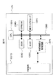
図9は、ホスト機器100が有するフラッシュ領域900内の構成を示した図である。
【0043】
ホスト機器100にダウンロードされたドライバのうち、一部分は使用後も破棄されずに、ホスト機器100内のフラッシュ領域900にドライバ情報とともに格納される。ホスト機器100は、図2のステップ303において、MMC120から送信されたドライバ情報のうち、ホスト機器100の構成、及び利用するアプリケーションの種別に合致する一つ、もしくは複数のドライバ情報と、ドライバライブラリ910に格納されたドライバ情報912とを照合する。同一のドライバがフラッシュ領域900に存在する場合、ホスト機器100は、ドライバライブラリ910内のドライバ領域914から該当するドライバを読み出して使用することが出来る。適当なドライバが見つからない場合、ホスト機器100は、MMC120を通常の仕様の下で利用する。尚、ドライバが暗号化されている場合は、ドライバの復号処理をおこなう。ドライバを利用する際はハッシュ値の計算をおこない、ドライバ情報が含むドライバのハッシュ値と一致しているかの確認をおこなうのが望ましい。ドライバ情報ファイルはカード内のドライバ情報ファイルに準ずる仕様を有する。
【0044】
MMC120においては、アップロードモジュール140及び暗号処理機能付きメモリ装置170は、コントローラチップ150の外に配置してもよく、フラッシュメモリ160は、コントローラチップ150の中に配置してもよい。またフラッシュメモリ160内にコントローラチップ150を配置してもよい。
【0045】
図5は、アップロードモジュール140を用いない場合で、かつ暗号処理機能付きメモリ装置170をICカードチップ520とし、コントローラチップ510の外部に配置した場合のMMC120の構成を示す図である。
【0046】
このような場合においてドライバアップデート機能を実行しようとすると、フラッシュメモリチップ160においてドライバ情報が格納されている場所をホスト機器100が保持するか、MMC120内のレジスタにドライバ情報を保持する等、ホスト機器100及びMMC120との間で、ドライバ情報の場所を特定する取り決めがなされている必要がある。この時、ホスト機器100は、MMC120からドライバ情報を読み出し、その中の情報に含まれるパスから目的のドライバを読み出す。
【0047】
図6は、図5に示すMMC120において、ホスト機器100がMMC120からドライバ情報を読み出す処理を示したフローチャートである。
【0048】
ホスト機器100は、MMC120を活性化するために電源供給をおこなう(601)。電源の供給が開始されたMMC120は、ICカードチップ520の起動をおこなう(651)。次にホスト機器100は、MMC120の初期化を指示する(603)。MMC120は、この命令に応じ自身の初期化を行う(655)。MMC120の初期化が成功しなかった場合(604)、ホスト機器100はMMC120の初期化を再試行する。
【0049】
MMC120の初期化が成功したら、ホスト機器100は、定められたアドレスからドライバ情報の読み出しをおこなう(605)。MMC120内のコントローラチップ510は、ホスト機器100の要求に従いフラッシュメモリチップ160からドライバ情報を読み出し、ホスト機器100に送信する(659)。ホスト機器100は、受信したドライバ情報をもとにドライバの選択をおこなう。この時、必要ならばシーケンスコマンドファイルを読みだし、MMC120とホスト機器100の間で定まった手順を要する処理をおこなっても良い。これは図3のオプショナルシーケンス380に相当するものである(607)。
【0050】
次いでホスト機器100は、MMC120に対しドライバの送信を要求する(609)。MMC120は、ホスト機器100が指定したアドレス及び容量に従ってフラッシュメモリチップ160からドライバの読み出しを行い、ホスト機器100に送信する(661)。尚、ホスト機器100が有するドライバライブラリ910にホスト機器100が使用するドライバが格納されているならば、ホスト機器100は、それを読み出して利用する(611)。ホスト機器100内のドライバライブラリ910もしくはMMC120から読み出されたドライバは、ホスト機器100に登録され(613)、以後このドライバの機能を用いるアプリケーションによって利用される(617)。
【0051】
本実施形態によれば、上述の構成を有することで、アップロードモジュール140を有する場合よりも低コストで、かつチップ面積を抑えてMMC120を作成することができる。
【0052】
また、ある特定の期間、特定の指示の下で特定の命令が発行された場合だけ、ドライバ情報を読み出す命令を発行するようなモジュールをMMC120に追加すれば、ホスト機器100から要求されるドライバ情報の位置に関する情報及び取り決めに対し、カード内のフラッシュメモリチップ160内のドライバ情報を配置する際の自由度が増す。具体的には、MMC120が転送モードに入って最初に発行されたREAD命令に応答して無条件でアドレスの変換をおこない特定の番地からドライバ情報を読み出す場合等が該当する。
【0053】
ドライバは、暗号化あるいは圧縮化されていたり、ID・ハッシュ値などの情報を含んでいても良い。MMC120が暗号処理機能付きメモリ装置170を含んでいない場合、認証等の作業はホスト機器100がおこなわなければならない。また、MMC120が暗号処理機能付きメモリ装置170を含んでいる場合でも、ホスト機器100が認証等の作業をやってもよい。
【0054】
図7は、アップロードモジュール140を有しないMMC120としてJava搭載の携帯端末を想定し、WAP(Wireless Application Protocol)のサービスを実現する構成を示した図である。ただし、本図の場合、図4で示した初期化アプリケーション430は、WAPアプリケーション760に含まれている。WAPアプリケーション760は、MMC120上のWIMの機能を利用するために、ICカードチップ520にアクセスするためのドライバをMMC120より読み出し利用する。
【0055】
MMC120に含まれるドライバ情報及びドライバは、MMC120の発行時に登録された後、ユーザによってその内容が変更されないほうが好ましい。ただし、新しいホスト機器に対応するため、又はドライバ情報の修正のためにドライバ情報及びドライバの内容を変更する必要がある。
【0056】
図10は、ドライバ情報及びドライバの内容を変更する処理を示したフローチャートである。はじめにホスト機器100は、MMC120からドライバを読み込み、MMC120のセキュリティ処理を利用可能な状態にする。ホスト機器100は、MMC120の暗号処理機能付きメモリ装置170に登録されたドライバ情報更新アプリケーションの起動をMMC120に指示する(1001)。暗号処理機能付きメモリ装置170は、ドライバ情報更新アプリケーションを起動し、ホスト機器100に応答を返す(1051)。
【0057】
応答を受けたホスト機器100は、暗号化された電子署名、ドライバ情報、及びドライバをMMC120に送信する(1003)。電子署名等の暗号化は、共通鍵又は公開鍵(秘密鍵)を用いておこなわれる。暗号処理機能付きメモリ装置170は、共通鍵又は秘密鍵(公開鍵)を用いて暗号化された電子署名等を復号する(1053)。ここで使用される暗号鍵の鍵情報は、いずれも発行者によって秘密に管理されていることが望ましい。暗号化されたドライバはネットワーク、CD−ROMなどを通じて配布される。また、配布されるドライバ等は、暗号化によりユーザが容易に改竄できないようにされている。
【0058】
ドライバ更新アプリケーションは、アプリケーション自身が有する平文の電子署名と復号化された電子署名と比較して、このドライバが正しい発行者によって提供された、又は正しい発行者によって認可を受けた製造者により提供されたものかどうかの確認をおこなう(1055)。電子署名が一致しない場合、ドライバ更新アプリケーションは、その旨をホスト機器100に伝え処理を終了する。電子署名が一致した場合、ドライバ更新アプリケーションは、復号化されたドライバをフラッシュメモリチップ160のドライバが格納されている領域に追加して登録・更新を行う。又復号化されたドライバ情報をフラッシュメモリチップ160のドライバ情報が格納されている領域に追加して登録・更新を行う。
【0059】
ドライバの登録は、同じドライバ情報をもつ(製造者、対応機種等)ドライバMMC120内に存在しない場合におこなわれ、ドライバの変更は同じドライバ情報をもつファイルが存在し、バージョンが古いものがある場合に適用される。登録・変更が終了するとMMC120はその旨をホスト機器100に送信する。
【0060】
図11は、アップロードモジュールチップ1140をコントローラチップ1110の外部に配置したMMC120の構成を示す図である。この場合も同様にアップロード機能を実現することが出来る。ただし、アップロードモジュール1140は、MMCインターフェイス制御回路1210を持ち、このMMCインターフェイス制御回路1210を介してホスト機器100と通信を行う。アップロード処理終了後、コントローラチップ1110は、アップロードモジュール1140を単にMMCインターフェイス 制御回路1210として用いてもよい。
【0061】
【発明の効果】
本発明によれば、ホスト機器は、必要なときに必要なドライバをMMC又はネットワーク等からダウンロードするだけでよく、ホスト機器の記憶領域を圧迫することなく、ホスト機器とMMC等の記憶装置の入出力の互換性を高めるという効果を奏することが出来る。
【図面の簡単な説明】
【図1】MMC120の内部構成を示す図である。
【図2】アップロード処理の手順を示すフローチャートである。
【図3】アップロード処理の手順を示すフローチャートである。
【図4】MMC120の具体的な使用例を表す図である。
【図5】暗号処理機能付きメモリ装置としてICカードを用い、アップロードモジュール140を用いないMMC120を示す図である。
【図6】図5に示すMMC120のアップロード処理の手順を示すフローチャートである。
【図7】MMCが120の具体的な使用例を示す図である。
【図8】アップロードモジュール140内部のモジュール構成を示した図である。
【図9】ホスト機器100内のフラッシュメモリ領域900の構成を表した図である。
【図10】ホスト機器100がMMC120にドライバ及びドライバ情報の登録、更新をおこなう手順を示したフローチャートである。
【図11】アップロードモジュールをコントローラチップの外部に配置したMMC120を示す図である。
【図12】MMC120の内部構成を示す図である。
【図13】暗号処理機能付きメモリ装置170の構成を示した図である。
【図14】標準メモリカードコマンドで復号処理をおこなう際の手順を示したフローチャートである。
【符号の説明】
100…ホスト機器、120…MMC、140…アップロードモジュール、150…コントローラチップ、160…フラッシュメモリチップ、170…暗号処理機能付きメモリ装置、410…ホスト端末外部端子、430…初期化アプリケーション、520…ICカードチップ。[0001]
BACKGROUND OF THE INVENTION
The present invention relates to a storage device having a security function, a host device into which the storage device can be inserted, and a host device into which the storage device is inserted, and a memory card having a flash memory chip and a controller and a device into which the memory card can be inserted And a terminal device in which a memory card is inserted.
[0002]
[Prior art]
MultiMediaCard (“MultiMediaCard” is a registered trademark of Infineon Technologies AG. Hereinafter referred to as “MMC”) includes external power supply terminals, clock input terminals, command input / output terminals, data input / output terminals, ground terminals, and CS terminals. And a flash memory including a memory element and a microcomputer chip for controlling the flash memory. The MMC operates when power is supplied from an external terminal, and transmits / receives electrical signals to / from an external device connected to the external terminal (hereinafter referred to as “host device”), such as a mobile phone, through the external terminal. By doing so, data read / write and transfer modes of the flash memory, conversion of data transfer units, and the like are performed. Currently, the MMC is used as a small storage for storing and reading out music data and image data.
[0003]
[Problems to be solved by the invention]
New functions can be provided by adding modules or chips to the MMC. Conventionally, when a host device uses a new function added to the MMC, the host device has to download software (driver) corresponding to the new function of the MMC from another device or the like. Further, the host device needs to store and set a driver corresponding to the MMC for each MMC connected to the host device, and there is a problem that a large memory capacity is consumed in the host. Furthermore, there is a problem in that convenience is low because a user having a host device needs a special operation when using the MMC. In addition, even if functions newly added to the MMC are the same as the functions, it is necessary for the host device to require a different driver due to a difference in the mounting method in the MMC and a difference in the version of the MMC specification. There was a problem.
[0004]
An object of the present invention is to provide a module for operating an MMC having a new function.
[0005]
[Means for Solving the Problems]
In order to achieve the above object, the present invention provides a storage device for storing data, an external terminal connected to an external device, and a flash that stores a driver used when the external device uses the storage device. The memory has a control unit that controls the operation of the storage device, and the control unit reads a driver stored in the flash memory in accordance with an instruction from the external device and transmits the driver to the external device via the external terminal. The configuration.
[0006]
As another embodiment of the present invention, a storage device for storing data, an external terminal connected to an external device, a flash memory composed of a nonvolatile storage medium, and an operation of the storage device are controlled. And a control unit having information indicating a flash memory area in which software used when the external device uses the storage device is stored, and in accordance with an instruction from the external device The software stored in the memory area may be read using information and transmitted to an external device via an external terminal.
[0007]
Furthermore, the control unit can be configured to include an encryption processing unit that encrypts and decrypts data.
[0008]
The encryption processing unit may be an IC card chip.
[0009]
Further, in the present invention, the software is encrypted, and when the control unit reads out the software in accordance with an instruction from the external device, the control unit decrypts the software using the encryption processing unit and transfers the software to the external device. It can be set as the structure which transmits.
[0010]
As another embodiment of the present invention, a storage device for storing data, an external terminal connected to an external device, a flash memory configured with a non-volatile storage medium, and an operation of the storage device are controlled. A control unit that performs encryption and decryption of data, and the control unit stores an area of the flash memory in which software used when an external device uses a storage device is stored. The software stored in the flash memory area is read using the information according to instructions from the external device, decrypted using the encryption processing unit, and transmitted to the external device via the external terminal. It is good also as composition to do.
[0011]
DETAILED DESCRIPTION OF THE INVENTION
FIG. 1 is a diagram showing an internal configuration of an MMC to which the present invention is applied. The
[0012]
The MMC 120 includes an MMC
[0013]
The
[0014]
FIG. 12 is a diagram illustrating the configuration of the
[0015]
The
[0016]
The
[0017]
FIG. 13 is a diagram showing a configuration of the
[0018]
The
[0019]
2 and 3 are flowcharts showing the flow of processing performed when the
[0020]
First, the
[0021]
The
[0022]
When the
[0023]
If the
[0024]
Driver information includes driver information size, driver type, manufacturer name, registration date, version number, capacity, program type, compatible terminal, encrypted key information and corresponding application information, driver Information such as the hash value of the data, the path of the sequence command file, and the path to the storage location is included. The size of the driver information is the size of the driver information represented by a fixed bit length. The type of driver indicates what the driver is used for. The manufacturer name is a registration number of the manufacturer or a character string that can specify the registrant. The registration date / time indicates the date / time when the driver was registered in the card. The version number indicates the revision number of the driver. The capacity indicates the capacity of the driver program required for the host, and the type of program indicates the format (binary code, Java applet, DLL, source program, etc.) when the program is distributed. The corresponding terminal indicates the vendor name (for example, NTT 503i series) of the corresponding host device. The key information and application information when encrypted include DF including key information set in the
[0025]
The driver information may be stored in the
[0026]
After
[0027]
FIG. 14 is a flowchart of the driver reading process when the driver is encrypted. The upload
[0028]
Returning to FIG. 3, the description will be continued.
[0029]
When a driver transmission request is issued from the host device 100 (305), the upload
[0030]
FIG. 4 is a diagram illustrating an example in which a WAP (Wireless Application Protocol) service is performed on the assumption that a Java-equipped mobile terminal is used as the
[0031]
The
[0032]
The host device
[0033]
After the uploading operation is completed, the application included in the
[0034]
As an external terminal other than the
[0035]
When using an external terminal of an arbitrary specification, the
[0036]
With this mechanism, the
[0037]
FIG. 8 is a diagram showing an internal configuration of the upload
[0038]
The upload
[0039]
The memory
[0040]
When the
[0041]
When the CMD0 is issued from the
[0042]
FIG. 9 is a diagram showing a configuration in the
[0043]
A part of the driver downloaded to the
[0044]
In the
[0045]
FIG. 5 is a diagram showing a configuration of the
[0046]
If an attempt is made to execute the driver update function in such a case, the
[0047]
FIG. 6 is a flowchart showing a process in which the
[0048]
The
[0049]
If the initialization of the
[0050]
Next, the
[0051]
According to the present embodiment, by having the above-described configuration, the
[0052]
Further, if a module that issues an instruction to read driver information is added to the
[0053]
The driver may be encrypted or compressed, and may include information such as an ID / hash value. If the
[0054]
FIG. 7 is a diagram illustrating a configuration for realizing a WAP (Wireless Application Protocol) service assuming a mobile terminal equipped with Java as the
[0055]
It is preferable that the driver information and the driver included in the
[0056]
FIG. 10 is a flowchart showing processing for changing driver information and driver contents. First, the
[0057]
Upon receiving the response, the
[0058]
The driver update application is provided by the manufacturer for which this driver was provided by or authorized by the correct issuer, as compared to the plaintext digital signature and the decrypted digital signature that the application itself has. It is confirmed whether it is a proper one (1055). If the electronic signatures do not match, the driver update application notifies the
[0059]
Driver registration is performed when the
[0060]
FIG. 11 is a diagram showing a configuration of the
[0061]
【The invention's effect】
According to the present invention, the host device need only download the necessary driver from the MMC or the network when necessary, and the host device and the storage device such as the MMC can be inserted without squeezing the storage area of the host device. The effect of improving the compatibility of output can be produced.
[Brief description of the drawings]
FIG. 1 is a diagram showing an internal configuration of an
FIG. 2 is a flowchart showing a procedure of upload processing.
FIG. 3 is a flowchart showing a procedure of upload processing.
4 is a diagram illustrating a specific usage example of
5 is a diagram showing an
6 is a flowchart showing a procedure of upload processing of the
FIG. 7 is a diagram illustrating a specific usage example where the MMC is 120;
FIG. 8 is a diagram showing a module configuration inside the upload
9 is a diagram showing a configuration of a
FIG. 10 is a flowchart showing a procedure in which the
FIG. 11 is a diagram showing an
12 is a diagram showing an internal configuration of an
FIG. 13 is a diagram showing a configuration of a memory device with an encryption processing function.
FIG. 14 is a flowchart showing a procedure for performing a decoding process using a standard memory card command.
[Explanation of symbols]
DESCRIPTION OF
Claims (7)
外部機器と接続される外部端子と、
不揮発性の記憶媒体で構成され、前記外部機器が該記憶装置を使用する際に用いるソフトウエアが格納されたフラッシュメモリと、
該記憶装置の動作を制御するコントローラチップとを有し、
前記コントローラチップは、
前記外部端子の制御を行う外部端子制御回路と、
前記ソフトウエアを前記外部機器に送信するアップロードモジュールと、
前記コントローラチップ内の各回路を制御するコントローラモジュールとを有し、
前記アップロードモジュールは、
前記外部端子制御回路と前記コントローラモジュールとに接続され、
前記外部機器と通信を行い、前記外部機器に対して前記ソフトウエアを送信するために1または複数のモジュールを呼び出して処理を行うモジュール制御装置と、
前記フラッシュメモリから読み出した前記ソフトウエアの一部もしくは全部を格納するRAMと、
前記アップロードモジュールの初期化を行う初期化モジュールと、
前記外部機器からの前記ソフトウエアの読み出し要求に対して、前記ソフトウエアが格納されている前記フラッシュメモリの領域へのアドレスの補完を行うアドレス変換モジュールと、
前記アップロードモジュールの終了処理を行う終了モジュールとを有して、
該記憶装置が前記外部機器から電源を供給された際に、前記外部機器の指示に応じて、前記フラッシュメモリに格納されている前記ソフトウエアを読み出し、前記外部端子を介して前記外部機器に送信し、
該記憶装置は、
前記アップロードモジュールによる前記ソフトウエアの送信終了後、前記アップロードモジュールと前記外部端子制御回路との接続を論理的に解除し、前記外部端子制御回路と前記コントローラモジュールとを論理的に接続することを特徴とする記憶装置。A storage device for storing data,
An external terminal connected to an external device;
A flash memory configured with a non-volatile storage medium and storing software used when the external device uses the storage device;
A controller chip for controlling the operation of the storage device,
The controller chip is
An external terminal control circuit for controlling the external terminal;
An upload module for transmitting the software to the external device;
A controller module for controlling each circuit in the controller chip,
The upload module
Connected to the external terminal control circuit and the controller module;
A module controller that communicates with the external device and calls and processes one or more modules to transmit the software to the external device;
RAM for storing a part or all of the software read from the flash memory;
An initialization module for initializing the upload module;
An address conversion module for complementing an address to the area of the flash memory in which the software is stored in response to a read request of the software from the external device;
An end module that performs an end process of the upload module,
When the power is supplied from the external device to the storage device, the software stored in the flash memory is read in accordance with an instruction from the external device and transmitted to the external device via the external terminal And
The storage device
After the transmission of the software by the upload module is completed, the connection between the upload module and the external terminal control circuit is logically disconnected, and the external terminal control circuit and the controller module are logically connected. A storage device.
外部機器と接続される外部端子と、An external terminal connected to an external device;
不揮発性の記憶媒体で構成され、前記外部機器が該記憶装置を使用する際に用いるソフトウエアが格納されたフラッシュメモリと、A flash memory configured with a non-volatile storage medium and storing software used when the external device uses the storage device;
該記憶装置の動作を制御するコントローラチップと、A controller chip for controlling the operation of the storage device;
前記ソフトウエアを前記外部機器に送信するアップロードモジュールチップとを有し、An upload module chip for transmitting the software to the external device;
前記アップロードモジュールチップは、The upload module chip is
前記コントローラチップに接続され、Connected to the controller chip,
前記外部端子の制御を行う外部端子制御回路と、An external terminal control circuit for controlling the external terminal;
前記外部機器と通信を行い、前記外部機器に対して前記ソフトウエアを送信するために1または複数のモジュールを呼び出して処理を行うモジュール制御装置と、A module control device that communicates with the external device and calls and processes one or more modules to transmit the software to the external device;
前記フラッシュメモリから読み出した前記ソフトウエアの一部もしくは全部を格納するRAMと、RAM for storing part or all of the software read from the flash memory;
前記アップロードモジュールチップの初期化を行う初期化モジュールと、An initialization module for initializing the upload module chip;
前記外部機器からの前記ソフトウエアの読み出し要求に対して、前記ソフトウエアが格納されている前記フラッシュメモリの領域へのアドレスの補完を行うアドレス変換モジュールと、An address conversion module that complements an address to the area of the flash memory in which the software is stored in response to a request to read the software from the external device;
前記アップロードモジュールチップの終了処理を行う終了モジュールとを有して、An end module that performs end processing of the upload module chip,
該記憶装置が前記外部機器から電源を供給された際に、前記外部機器の指示に応じて、前記フラッシュメモリに格納されている前記ソフトウエアを読み出し、前記外部端子を介しWhen the power is supplied from the external device to the storage device, the software stored in the flash memory is read in accordance with an instruction from the external device, via the external terminal て前記外部機器に送信し、送信終了後は前記外部端子制御回路として動作することを特徴とする記憶装置。The storage device is configured to transmit to the external device and operate as the external terminal control circuit after the transmission ends.
外部機器と接続される外部端子と、
不揮発性の記憶媒体で構成され、前記外部機器が該記憶装置を使用する際に用いるソフトウエアが格納されたフラッシュメモリと、
該記憶装置の動作を制御するコントローラチップとを有し、
前記フラッシュメモリには、前記ソフトウエアに関する情報および前記ソフトウエアが前記フラッシュメモリに格納されている領域を示す情報からなるソフトウエア情報が格納され、
前記コントローラチップは、
前記外部端子の制御を行う外部端子制御回路と、
前記ソフトウエアを前記外部機器に送信するアップロードモジュールと、
前記コントローラチップ内の各回路を制御するコントローラモジュールとを有し、
前記アップロードモジュールは、
前記外部端子制御回路と前記コントローラモジュールとに接続され、
前記外部機器と通信を行い、前記外部機器に対して前記ソフトウエア情報および前記ソフトウエアを送信するために1または複数のモジュールを呼び出して処理を行うモジュール制御装置と、
前記フラッシュメモリから読み出した前記ソフトウエア情報および前記ソフトウエアの一部もしくは全部を格納するRAMと、
前記アップロードモジュールの初期化を行う初期化モジュールと、
前記外部機器からの前記ソフトウエア情報の読み出し要求に対して、前記ソフトウエア情報が格納されている前記フラッシュメモリの領域へのアドレスの補完を行うアドレス変換モジュールと、
前記アップロードモジュールの終了処理を行う終了モジュールとを有して、
該記憶装置が前記外部機器から電源を供給された際に、前記ソフトウエア情報を前記外部端子を介して前記外部機器に送信し、前記外部機器の指示に応じて、前記フラッシュメモリの領域に格納されている前記ソフトウエアを前記ソフトウエア情報を用いて読み出し、前記外部端子を介して前記外部機器に送信し、
該記憶装置は、
前記アップロードモジュールによる前記ソフトウエアの送信終了後、前記アップロードモジュールと前記外部端子制御回路との接続を論理的に解除し、前記外部端子制御回路と前記コントローラモジュールとを論理的に接続することを特徴とする記憶装置。A storage device for storing data,
An external terminal connected to an external device;
A flash memory configured with a non-volatile storage medium and storing software used when the external device uses the storage device ;
A controller chip for controlling the operation of the storage device,
The flash memory stores software information including information about the software and information indicating an area where the software is stored in the flash memory.
The controller chip is
An external terminal control circuit for controlling the external terminal;
An upload module for transmitting the software to the external device;
A controller module for controlling each circuit in the controller chip,
The upload module
Connected to the external terminal control circuit and the controller module;
A module control device that communicates with the external device and calls and processes one or more modules to transmit the software information and the software to the external device;
RAM for storing the software information read from the flash memory and part or all of the software;
An initialization module for initializing the upload module;
In response to a request to read the software information from the external device, an address conversion module that complements an address to the area of the flash memory in which the software information is stored;
An end module that performs an end process of the upload module,
When the storage device is supplied with power from the external device, the software information is transmitted to the external device via the external terminal and stored in the flash memory area in accordance with an instruction from the external device. The software that is being read using the software information, transmitted to the external device via the external terminal ,
The storage device
After the transmission of the software by the upload module is completed, the connection between the upload module and the external terminal control circuit is logically disconnected, and the external terminal control circuit and the controller module are logically connected. A storage device.
外部機器と接続される外部端子と、An external terminal connected to an external device;
不揮発性の記憶媒体で構成され、前記外部機器が該記憶装置を使用する際に用いるソフトウエアが格納されたフラッシュメモリと、A flash memory configured with a non-volatile storage medium and storing software used when the external device uses the storage device;
該記憶装置の動作を制御するコントローラチップと、A controller chip for controlling the operation of the storage device;
前記ソフトウエアを前記外部機器に送信するアップロードモジュールチップとを有し、An upload module chip for transmitting the software to the external device;
前記フラッシュメモリには、前記ソフトウエアに関する情報および前記ソフトウエアが前記フラッシュメモリに格納されている領域を示す情報からなるソフトウエア情報が格納され、The flash memory stores software information including information about the software and information indicating an area in which the software is stored in the flash memory.
前記アップロードモジュールチップは、The upload module chip is
前記コントローラチップに接続され、Connected to the controller chip,
前記外部端子の制御を行う外部端子制御回路と、An external terminal control circuit for controlling the external terminal;
前記外部機器と通信を行い、前記外部機器に対して前記ソフトウエアを送信するために1または複数のモジュールを呼び出して処理を行うモジュール制御装置と、A module control device that communicates with the external device and calls and processes one or more modules to transmit the software to the external device;
前記フラッシュメモリから読み出した前記ソフトウエア情報および前記ソフトウエアの一部もしくは全部を格納するRAMと、RAM for storing the software information read from the flash memory and part or all of the software;
前記アップロードモジュールチップの初期化を行う初期化モジュールと、An initialization module for initializing the upload module chip;
前記外部機器からの前記ソフトウエアの読み出し要求に対して、前記ソフトウエアが格納されている前記フラッシュメモリの領域へのアドレスの補完を行うアドレス変換モジュールと、An address conversion module that complements an address to the area of the flash memory in which the software is stored in response to a request to read the software from the external device;
前記アップロードモジュールチップの終了処理を行う終了モジュールとを有して、An end module that performs end processing of the upload module chip,
該記憶装置が前記外部機器から電源を供給された際に、前記ソフトウエア情報を前記外部端子を介して前記外部機器に送信し、前記外部機器の指示に応じて、前記フラッシュメモリの領域に格納されている前記ソフトウエアを前記ソフトウエア情報を用いて読み出し、前記外部端子を介して前記外部機器に送信し、送信終了後は前記外部端子制御回路として動作することを特徴とする記憶装置。When the storage device is supplied with power from the external device, the software information is transmitted to the external device via the external terminal and stored in the flash memory area in accordance with an instruction from the external device. The storage device is characterized in that the software is read using the software information, transmitted to the external device via the external terminal, and operates as the external terminal control circuit after the transmission is completed.
データの暗号化及び復号化を行う暗号処理部を有することを特徴とする請求項1〜4のいずれか1項に記載の記憶装置。The controller chip is
Memory device according to claim 1, characterized in that it comprises an encryption unit for encrypting and decrypting data.
前記記憶装置を使用するためのソフトウエアを格納する記憶領域と、
前記記憶装置と接続される接続部と、
前記記憶装置に格納された前記ソフトウエアを読み出し、前記記憶領域に格納する手段とを有することを特徴とする機器。 A device connected to the storage device according to any one of claims 1 to 6 ,
A storage area for storing software for using the storage device;
A connection unit connected to the storage device;
An apparatus comprising: means for reading out the software stored in the storage device and storing the software in the storage area.
Priority Applications (1)
| Application Number | Priority Date | Filing Date | Title |
|---|---|---|---|
| JP2001207211A JP4236830B2 (en) | 2001-07-09 | 2001-07-09 | Storage device with upload function |
Applications Claiming Priority (1)
| Application Number | Priority Date | Filing Date | Title |
|---|---|---|---|
| JP2001207211A JP4236830B2 (en) | 2001-07-09 | 2001-07-09 | Storage device with upload function |
Publications (2)
| Publication Number | Publication Date |
|---|---|
| JP2003022427A JP2003022427A (en) | 2003-01-24 |
| JP4236830B2 true JP4236830B2 (en) | 2009-03-11 |
Family
ID=19043227
Family Applications (1)
| Application Number | Title | Priority Date | Filing Date |
|---|---|---|---|
| JP2001207211A Expired - Fee Related JP4236830B2 (en) | 2001-07-09 | 2001-07-09 | Storage device with upload function |
Country Status (1)
| Country | Link |
|---|---|
| JP (1) | JP4236830B2 (en) |
Families Citing this family (10)
| Publication number | Priority date | Publication date | Assignee | Title |
|---|---|---|---|---|
| JP4597568B2 (en) | 2003-07-15 | 2010-12-15 | パナソニック株式会社 | Secure device, information processing terminal, and information processing system |
| US20060059372A1 (en) * | 2004-09-10 | 2006-03-16 | International Business Machines Corporation | Integrated circuit chip for encryption and decryption having a secure mechanism for programming on-chip hardware |
| JP2006172122A (en) * | 2004-12-15 | 2006-06-29 | Toshiba Corp | Card storage device |
| KR100707308B1 (en) | 2005-06-13 | 2007-04-12 | 삼성전자주식회사 | Flash memory device having an MC interface and a memory system including the same |
| JP4852721B2 (en) * | 2007-01-25 | 2012-01-11 | 日本電産サンキョー株式会社 | Card reader and control method thereof |
| KR100823171B1 (en) | 2007-02-01 | 2008-04-18 | 삼성전자주식회사 | Computer system with partitioned flash translation layer and partitioning method of flash translation layer |
| US8862787B2 (en) | 2010-12-20 | 2014-10-14 | Intel Incorporation | Method and apparatus for integrating driver(s) of a portable device into the portable device |
| US9686460B2 (en) * | 2012-12-27 | 2017-06-20 | Intel Corporation | Enabling a metadata storage subsystem |
| JP2021163997A (en) | 2020-03-30 | 2021-10-11 | キヤノン株式会社 | Imaging devices, devices, communication methods, and programs |
| JP2021163998A (en) | 2020-03-30 | 2021-10-11 | キヤノン株式会社 | Imaging devices, devices, control methods, and programs |
-
2001
- 2001-07-09 JP JP2001207211A patent/JP4236830B2/en not_active Expired - Fee Related
Also Published As
| Publication number | Publication date |
|---|---|
| JP2003022427A (en) | 2003-01-24 |
Similar Documents
| Publication | Publication Date | Title |
|---|---|---|
| US7650503B2 (en) | Memory card | |
| US8176335B2 (en) | Removable computer with mass storage | |
| JP4391375B2 (en) | Information management apparatus and method, and program | |
| JP4308551B2 (en) | Memory card and host device | |
| US7213157B2 (en) | Integrated circuit for digital rights management | |
| TWI524275B (en) | Storage device and method of operating a storage device | |
| JP2002329180A (en) | Memory card having wireless communication function and data communication method thereof | |
| US11126753B2 (en) | Secure processor chip and terminal device | |
| JP3865629B2 (en) | Storage device | |
| US8032663B2 (en) | Information processing system, information processing apparatus and integrated circuit chip | |
| JP4236830B2 (en) | Storage device with upload function | |
| CN106056017A (en) | Intelligent card COS encrypting and downloading system | |
| US11907931B2 (en) | Method and system for managing virtual electronic card, secure chip, terminal and storage medium | |
| WO2007119594A1 (en) | Secure device and read/write device | |
| US9449453B2 (en) | Portable electronic entity and method for personalization of such an electronic entity | |
| US20150234646A1 (en) | Method for Installing Security-Relevant Applications in a Security Element of a Terminal | |
| CN116016168A (en) | Software function activation method, device, equipment and storage medium | |
| CN114499918B (en) | Security elements and methods | |
| CN114513294B (en) | Security elements and methods | |
| JPH10301854A (en) | Chip card and method for importing information on the same | |
| CN113704773A (en) | Relay protection safety chip operating system and communication method thereof | |
| JP4708754B2 (en) | Server client system, client, data processing method, and program | |
| JP2004334471A (en) | Information card | |
| CN114490108A (en) | Security element and method | |
| JP2022025986A (en) | Electronic information storage medium, program addition method, and program |
Legal Events
| Date | Code | Title | Description |
|---|---|---|---|
| A621 | Written request for application examination |
Free format text: JAPANESE INTERMEDIATE CODE: A621 Effective date: 20060112 |
|
| RD02 | Notification of acceptance of power of attorney |
Free format text: JAPANESE INTERMEDIATE CODE: A7422 Effective date: 20060112 |
|
| A977 | Report on retrieval |
Free format text: JAPANESE INTERMEDIATE CODE: A971007 Effective date: 20080408 |
|
| A131 | Notification of reasons for refusal |
Free format text: JAPANESE INTERMEDIATE CODE: A131 Effective date: 20080422 |
|
| A521 | Written amendment |
Free format text: JAPANESE INTERMEDIATE CODE: A523 Effective date: 20080623 |
|
| TRDD | Decision of grant or rejection written | ||
| A01 | Written decision to grant a patent or to grant a registration (utility model) |
Free format text: JAPANESE INTERMEDIATE CODE: A01 Effective date: 20081202 |
|
| A01 | Written decision to grant a patent or to grant a registration (utility model) |
Free format text: JAPANESE INTERMEDIATE CODE: A01 |
|
| A61 | First payment of annual fees (during grant procedure) |
Free format text: JAPANESE INTERMEDIATE CODE: A61 Effective date: 20081217 |
|
| R150 | Certificate of patent or registration of utility model |
Free format text: JAPANESE INTERMEDIATE CODE: R150 |
|
| FPAY | Renewal fee payment (event date is renewal date of database) |
Free format text: PAYMENT UNTIL: 20111226 Year of fee payment: 3 |
|
| FPAY | Renewal fee payment (event date is renewal date of database) |
Free format text: PAYMENT UNTIL: 20111226 Year of fee payment: 3 |
|
| S111 | Request for change of ownership or part of ownership |
Free format text: JAPANESE INTERMEDIATE CODE: R313111 |
|
| FPAY | Renewal fee payment (event date is renewal date of database) |
Free format text: PAYMENT UNTIL: 20111226 Year of fee payment: 3 |
|
| R350 | Written notification of registration of transfer |
Free format text: JAPANESE INTERMEDIATE CODE: R350 |
|
| FPAY | Renewal fee payment (event date is renewal date of database) |
Free format text: PAYMENT UNTIL: 20111226 Year of fee payment: 3 |
|
| FPAY | Renewal fee payment (event date is renewal date of database) |
Free format text: PAYMENT UNTIL: 20121226 Year of fee payment: 4 |
|
| FPAY | Renewal fee payment (event date is renewal date of database) |
Free format text: PAYMENT UNTIL: 20121226 Year of fee payment: 4 |
|
| FPAY | Renewal fee payment (event date is renewal date of database) |
Free format text: PAYMENT UNTIL: 20131226 Year of fee payment: 5 |
|
| S531 | Written request for registration of change of domicile |
Free format text: JAPANESE INTERMEDIATE CODE: R313531 |
|
| R350 | Written notification of registration of transfer |
Free format text: JAPANESE INTERMEDIATE CODE: R350 |
|
| LAPS | Cancellation because of no payment of annual fees |