JP4232065B2 - Electronics - Google Patents
Electronics Download PDFInfo
- Publication number
- JP4232065B2 JP4232065B2 JP36144399A JP36144399A JP4232065B2 JP 4232065 B2 JP4232065 B2 JP 4232065B2 JP 36144399 A JP36144399 A JP 36144399A JP 36144399 A JP36144399 A JP 36144399A JP 4232065 B2 JP4232065 B2 JP 4232065B2
- Authority
- JP
- Japan
- Prior art keywords
- case
- circuit board
- digital
- housing case
- reproduction
- Prior art date
- Legal status (The legal status is an assumption and is not a legal conclusion. Google has not performed a legal analysis and makes no representation as to the accuracy of the status listed.)
- Expired - Lifetime
Links
Images


Description
【0001】
【発明の属する技術分野】
本発明は電子機器に関し、例えば音楽データを再生し得る携帯型のディジタル再生装置に適用して好適なものである。
【0002】
【従来の技術】
近年、携帯型のディジタル再生装置として、半導体メモリを音楽データの記憶手段として用いるものが提案されており、当該半導体メモリから音楽データを再生して得られる音楽を楽しむようになされている。
【0003】
【発明が解決しようとする課題】
ところでかかるディジタル再生装置においては、携帯性を向上させるために、さらなる小型化が望まれている。
【0004】
本発明は以上の点を考慮してなされたもので、一段と小型化し得る電子機器を提案しようとするものである。
【0005】
【課題を解決するための手段】
かかる課題を解決するため本発明においては、円筒形状の筐体ケースと、筐体ケースの表面の所定部分に設けられた操作手段と、操作手段が操作されたときに当該操作手段と係合して操作信号を出力するための信号出力素子が配置され、当該信号出力素子が操作手段と対向して当該操作手段が操作されたときに係合するように、筐体ケース内に設けられた素子配置部材と、信号出力素子から出力される操作信号に基づいて所定の制御を行う制御素子が配置され、素子配置部材よりも筐体ケースの中心側に位置して素子配置部材が積層されるように筐体ケース内に設けられた回路基板とを設けるようにした。
【0006】
従って、筐体ケースの形状を損なうことなく、回路基板を容易に収納することができる。
【0007】
【発明の実施の形態】
以下図面について、本発明の一実施の形態を詳述する。
【0008】
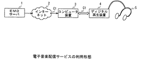
(1)電子音楽配信サービスの利用形態
近年、インターネットによるコンピュータネットワークを用いてディジタル音楽コンテンツを配信するEMD(Electric Music Distribution)と呼ばれる電子音楽配信サービスが提案されている。
【0009】
図1に示すように、この種の電子音楽配信サービスにおいては、コンテンツの供給を行うEMDサーバ1からインターネット2を介して家庭内のパーソナルコンピュータ(以下、これをコンピュータ装置と呼ぶ)3へディジタル音楽コンテンツC1を配信する。
【0010】
コンピュータ装置3では、EMDサーバ1から配信されたディジタル音楽コンテンツC1を内部のハードディスクにダウンロードし、これをユーザの操作に応じて再生することにより、ユーザが何時でも音楽を楽しめるようになされている。
【0011】
このような電子音楽配信サービスでは、EMDサーバ1からコンピュータ装置3へダウンロードしたディジタル音楽コンテンツC1をあたかもCD(Compact Disc)のように何時でも又何回でも再生し得る「買取」と呼ばれる購入方法が存在する一方で、料金設定を安くしたサービスとして再生可能期間や再生可能回数の再生制限を設けた「再生制限付」と呼ばれる新たな購入方法が存在する。
【0012】
従ってユーザは、EMDサーバ1からディジタル音楽コンテンツC1を「再生制限付」で購入した場合、当該購入したディジタル音楽コンテンツC1をコンピュータ装置3によって再生可能期間又は再生可能回数の範囲内で再生することができる。
【0013】
またコンピュータ装置3は、不揮発性の半導体フラッシュメモリを記憶手段として内蔵した携帯型のディジタル再生装置4とUSB(Universal Serial Bus)ケーブルを介して接続し得るようになされており、これによりディジタル音楽コンテンツC1をディジタルデータのままディジタル再生装置4の半導体フラッシュメモリにアップロードし得るようになされている。
【0014】
これによりユーザは、コンピュータ装置3のみならずディジタル再生装置4によっても「再生制限付」のディジタル音楽コンテンツC1を再生可能期間又は再生可能回数の範囲内で再生することができ、かくして高音質な音楽をヘッドフォン5を介して屋外でも気軽に楽しめるようになされている。
【0015】
実際上、図2(A)に示すように、EMDサーバ1からコンピュータ装置3にダウンロードされた「再生制限付」のディジタル音楽コンテンツC1は、ヘッダH1と音楽データD1とが一体となって構成され、当該ヘッダH1には再生可能期間、再生可能回数及び実際に再生した回数(以下、これを実再生回数と呼ぶ)等の再生制限に関する種々の情報が格納されている。
【0016】
次に図2(B)に示すように、コンピュータ装置3は、ディジタル音楽コンテンツC1をディジタルデータのままディジタル再生装置4の半導体フラッシュメモリにアップロードする。
【0017】
ディジタル再生装置4は、ユーザの再生操作に応じて再生処理を実行する際、必ずヘッダH1の再生制限情報を読み取った後に音楽データD1を再生するようになされており、これによりヘッダH1で管理される再生制限情報を有効に活用し、不正な再生処理を防止している。
【0018】
ところで本実施の形態におけるディジタル再生装置4においては、RTC回路を搭載しておらず、このままでは時計機能によって再生可能期間を管理し得ないことから、ヘッダH1の再生制限情報を読み出した場合でも、再生可能期間の範囲内であるか否かを判定し得ず、ディジタル音楽コンテンツC1を無制限に再生されることが考えられる。
【0019】
このようなことを防止するため、ディジタル再生装置4は例え再生可能期間の範囲内であっても、ヘッダH1の再生制限情報によって規定された「再生可能回数(例えば2回)」の範囲内でのみ再生処理することを許可し、実際に再生したときに更新される「実再生回数」が「再生可能回数」に達したときには、再生処理を制限するようなプロテクトをかけるようになされている。
【0020】
但し図2(C)に示すようにディジタル再生装置4は、このままでは再生可能期間の範囲内であるにも係わらず2回だけしか再生し得ないことになるので、再度コンピュータ装置3と接続して当該コンピュータ装置3に内蔵されたRTC回路3Aから現在の時刻情報T1の供給を受け、当該時刻情報T1に基づいて再生可能期間の範囲内であるか否かを判定し、再生可能期間の範囲内であると認識したときには、ヘッダH1の「実再生回数」を「0」に書き換えるようになされている。
【0021】
これによりディジタル再生装置4は、再生可能期間の範囲内であるときにはヘッダH1の再生制限情報によって規定された「再生可能回数(例えば2回)」の制限を繰り返し利用して上述の再生処理を何度でも実行し得るようになされている。
【0022】
またディジタル再生装置4は、時刻情報T1に基づいて再生可能期間が終了していると認識したときには、ヘッダH1の「再生回数」を「0」に書き換えることなく再生処理を実行しないようにしている。
【0023】
このようにディジタル再生装置4は、上述のような「再生可能回数」までの再生処理及びコンピュータ装置3と接続したことによる再生可能期間のチェックを繰り返すことにより、再生可能期間の範囲内であれば「再生可能回数(2回)」までの再生処理を何度でも繰り返し実行し得ると共に、再生可能期間が終了したときには再生処理を制限し得るようになされている。
【0024】
これに対してディジタル再生装置4は、再生可能回数の再生制限だけが付加されたディジタル音楽コンテンツC1の場合には、その再生可能回数の範囲内で再生処理を実行し、再生可能回数分を再生したときには、それ以降の再生処理を実行しないようになされている。
【0025】
(2)ディジタル再生装置の全体構成
(2−1)ディジタル再生装置の構造
図3に示すように、ディジタル再生装置4においては、ほぼ円筒形状でなる筐体ケース10を有し、当該筐体ケース10の周側面に各種操作スイッチや操作ボタン及び表示部用の表示窓11等が設けられている。
【0026】
ここで、ディジタル再生装置4の表示窓11が設けられた側を正面とした場合、筐体ケース10を軸中心に45度ずつ回転したときのそれぞれの周側面について図4(A)〜(D)を用いて説明する。
【0027】
図4(A)に示すように、筐体ケース10の左側面には、当該筐体ケース10の長手方向(以下、これをケース長手方向と呼ぶ)の一端側に音量の上限を固定するための音量上限固定スイッチ12がスライド自在に設けられると共に、USB(Universal Serial Bus)コネクタが収納された孔部(図示せず)を開閉するようにプラスチック製のUSBコネクタカバー13が設けられている。
【0028】
実際にUSBコネクタカバー13は、USBコネクタの未使用時に孔部を閉塞して筐体ケース10と一体化されることにより当該USBコネクタを保護し、USBコネクタの使用時には孔部を開放することにより当該USBコネクタをUSBケーブル(図示せず)を介してコンピュータ装置3に接続させ得るようになされている。
【0029】
また図4(B)に示すように、筐体ケース10の正面には、そのほぼ中央部から一端にかけて音量アップボタン14、音量ダウンボタン15、早送りボタン16、早戻しボタン17、表示窓11及びシフトボタン18が順次設けられている。また筐体ケース10の一端面には、再生命令及び停止命令を入力し得る再生/停止ボタン19が設けられている。
【0030】
そして筐体ケース10の正面においては、表示窓11の下部に設けられた表示部(図示せず)が各種操作に応じた表示を行うことにより、その表示内容を表示窓11を介して提示させることができるようになされている。
【0031】
因みに、シフトボタン18は、これが押下されたままの状態で早送りボタン16が押下されると、当該早送りボタン16と共に再生モードを切り換えるための操作ボタンとして機能する。またシフトボタン18は、これが押下されたままの状態で早戻しボタン17が押下されると、当該早戻しボタン17と共に音質モードを切り換えるための操作ボタンとしても機能する。
【0032】
さらに図4(C)に示すように、筐体ケース10の右側面には、その一端側にホールドスイッチ20がスライド自在に設けられ、当該ホールドスイッチ20を例えば筐体ケース10の一端側にスライドさせることにより各種操作ボタンの入力を無効にし、この状態を維持し得るようになされている。
【0033】
これに加えて図4(D)に示すように、筐体ケース10の背面には、その他端側に単3サイズの駆動用乾電池21を装填し得る乾電池収納部22が設けられると共に、当該乾電池収納部22を閉塞する蓋部23が着脱自在に取り付けられている。
【0034】
これにより乾電池収納部22においては、蓋部23が取り外されると、内部に駆動用乾電池21を装填し、又は当該内部から駆動用乾電池21を取り出すことができ、また内部に駆動用乾電池21が装填された状態で蓋部23が取り付けられると、当該蓋部23によって駆動用乾電池21を脱落することを防止して保持し得るようになされている。
【0035】
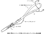
また筐体ケース10の背面には、その一端側にヘッドホンジャック24を保持するジャック保持部25と、当該筐体ケース10を上着の胸ポケット等に取り付けるためのクリップ部26とがケース長手方向に沿って並設されると共に、当該ジャック保持部25とクリップ部26との隣接部分で、かつディジタル再生装置4の重心からずれた所定位置に環状のストラップ金具27が設けられている。
【0036】
このストラップ金具27は、筐体ケース10の背面に対してジャック保持部25に接する姿勢からクリップ部26に接する姿勢までのほぼ180度の範囲内で自在に回動し得るようになされており、当該ストラップ金具27を起こすことにより各種ストラップを容易に取り付け、又は取り外すことができるようになされている。
【0037】
ここでディジタル再生装置4においては、ハードディスクドライブ等のように機械的な記録再生機構を有する記録再生装置とは異なり、図1について上述したように、内部の半導体フラッシュメモリに対してディジタル音楽コンテンツC1を記録再生することにより、振動が加えられるような環境下でも、音飛び等を生じさせることなくディジタル音楽コンテンツC1の音楽データD1を再生し得るようになされている。
【0038】
このため、かかるディジタル再生装置4においては、図5に示すように、通常、ヘッドホンコード28に設けられたプラグ29をヘッドホンジャック24に差し込むことにより、半導体フラッシュメモリから音楽データD1を再生して得られた音楽をヘッドホン5を介して聴くことができるようになされているものの、このときストラップ金具27に帯状の首掛け用のストラップ31を取り付けることにより首からぶら下げた状態で使用し得るようになされている。
【0039】
ところでディジタル再生装置4は、駆動用乾電池21を除くと25〔g〕程度の重量を有し、当該ディジタル再生装置4を構成する各種部品のほとんどがケース長手方向の一端側に設けられている。またディジタル再生装置4は、例えば23〔g〕程度の重量を有する駆動用乾電池21がケース長手方向の他端側に設けられた乾電池収納部22内に装填されるため、当該駆動用乾電池21が装填されたときには重心がケース長手方向のほぼ中央部となる。
【0040】
そしてディジタル再生装置4においては、図6に示すように、首掛け用のストラップ31が用いられて首からぶら下げられた場合、支点となるストラップ金具27の取付け位置が重心よりもケース長手方向に沿った一端側の所定位置にあるため、筐体ケース10の他端側がほぼ鉛直下方向を向き、その分、筐体ケース10の一端面に設けられた再生/停止ボタン19がほぼ鉛直上方向を向くような姿勢を維持するようになされている。
【0041】
これによりディジタル再生装置4においては、首からぶら下げられた場合、ユーザが筐体ケース10の周側面を握持するだけで、親指を再生/停止ボタン19に容易に触れさせて操作し得るようになされている。
【0042】
因みにディジタル再生装置4においては、図5からも明らかなように、首掛け用のストラップ31にヘッドホンコード28を保持する所定のコード保持部32が設けられており、当該首掛け用のストラップ31を用いて首からぶら下げて使用するとき、ヘッドホンコード28の引回しが煩雑になることを防止し得るようになされている。
【0043】
またディジタル再生装置4においては、図7に示すように、ジャック保持部25が楔状に形成され、ヘッドホンジャック24がその円筒状のプラグ差込み孔の軸をケース長手方向に対して傾斜させるようにしてジャック保持部25に保持されている。
【0044】
従ってディジタル再生装置4においては、プラグ29を筐体ケース10の一端側からケース長手方向に対して傾斜させてヘッドホンジャック24に差し込むことができ、これによりプラグ29とヘッドホンコード28との接続部分を再生/停止ボタン19から比較的遠ざけ、かくしてプラグ29とヘッドホンコード28との接続部分により再生/停止ボタン19の操作性が損なわれることを防止し得るようになされている。
【0045】
これに加えて、ディジタル再生装置4においては、図8に示すように、板状でなるクリップ部26の一端側がジャック保持部25に埋設された支軸(図示せず)に枢支され、当該クリップ部26の他端側を筐体ケース10の背面に対して所定角度範囲内で回動させるようになされている。
【0046】
これによりディジタル再生装置4においては、上着の胸ポケット33を筐体ケース10の他端側からその背面とクリップ部26との間に挟み込むようにして、当該胸ポケット33に取り付けることができる。
【0047】
そしてディジタル再生装置4においては、このように胸ポケット33に取り付けられた場合にも、再生/停止ボタン19を胸ポケット33から出した姿勢を維持し、かくして再生/停止ボタン19の操作性が損なわれることを防止し得るようになされている。
【0048】
ここで、筐体ケース10においては、図9に示すように、正面側の一端から他端までを構成する正面側ケース35と、背面の一端側を構成する背面側ケース36と、当該背面の他端側を構成する蓋部23と、再生/停止ボタン19を保持するボタン保持部37とから構築されている。
【0049】
正面側ケース35、背面側ケース36、蓋部23及びボタン保持部37は、それぞれPC(Polycarbonate)樹脂と、ABS(Acrylonitrile Butadiene Styrene)樹脂とを所定の割合で混合してなる合成樹脂によって成形されている。
【0050】
そして正面側ケース35は、その単一部材により図4(D)について上述した乾電池収納部22を他端側に形成している。また正面側ケース35の一端側と、背面側ケース36との間に形成される収納空間には、表示部保護部材40と、表示部41と、サブ回路基板42と、メイン回路基板43と、スイッチ回路基板44とが順次積層されて収納されている。因みに、スイッチ回路基板44は、音量上限固定スイッチ12及びホールドスイッチ20用のスイッチ回路素子44A及び44Bが実装されたフレキシブル基板でなり、背面側ケース36の内部に固定されている。
【0051】
実際上、乾電池収納部22においては、図10(A)及び(B)に示すように、駆動用乾電池21の外径に応じた内径を有する円筒形状の収納空間を有し、ケース長手方向に沿った一端には、導電性の金属線によりコイル状に形成された負極端子45が配置され、当該ケース長手方向に沿った他端には、導電性の金属材により例えば円板状に形成された正極端子46が配置されている。
【0052】
この場合、乾電池収納部22においては、負極端子45の一端がメイン回路基板43に直接電気的に接続され、正極端子46はこれと一体に形成された板状の導通板47を介してメイン回路基板43に電気的に接続されている。
【0053】
そして乾電池収納部22の底には、ケース長手方向の一端から他端に渡って溝部22Aが形成され、当該溝部22Aに導通板47が嵌合されている。この際、溝部22Aの深さは、導通板47の0.2〔mm〕程度の厚みに応じて選定されており、これにより導通板47を乾電池収納部22の内側面から収納空間に突出させないようになされている。
【0054】
また乾電池収納部22の底には、ケース長手方向に沿った一端から他端に渡って、0.1〔mm〕程度の厚みを有するシート状のシリアルラベル48が導体板47を覆うように貼着されている。
【0055】
シリアルラベル48は、図11(A)及び(B)に示すように、例えば、接着力の比較的強いアクリル系の感圧式接着剤層49と、アルミニウム層50と、PET(polyethylene terephthalate)でなる絶縁性の印刷用樹脂層51と、透明フィルム52とが順次積層されて形成され、当該アルミニウム層50の厚みが適宜選択されることにより、ある程度の硬性を有し、当該シリアルラベル48自体の破れ等の破損を防止し得るようになされている。
【0056】
因みにシリアルラベル48においては、印刷用樹脂層51の一面に駆動用乾電池21の装填方向を示す絵柄53と、シリアルラベル48が貼着されるディジタル再生装置4個々の製造番号を示す文字54及び2次元バーコード55とが印刷され、当該印刷用樹脂層51の一面に透明フィルム52がラミネートされていることにより絵柄53や文字54等が保護されている。
【0057】
従って乾電池収納部22(図10(A)及び(B))においては、シリアルラベル48の有する接着力及び硬性により、溝部22Aから導通板47が浮いて駆動用乾電池21の周側面に傷を付ける等して破損させることを防止し得ると共に、当該シリアルラベル48の有する絶縁性により駆動用乾電池21の周側面と、導通板47とを絶縁し得るようになされている。
【0058】
そして乾電池収納部22においては、このように、導通板47を溝部22Aに嵌合させると共に、当該導通板47と、駆動用乾電池21の周側面との絶縁に0.1〔mm〕程度の厚みを有するシリアルラベル48を用いることにより、乾電池収納部22の内径を駆動用乾電池21の14.5〔mm〕程度の外径とほぼ同程度に選定することができる。
【0059】
また乾電池収納部22においては、その肉厚を破損から保護し得るように選定することにより、内径及び肉厚に応じて当該乾電池収納部22の外径を17〔mm〕程度に選定することができ、かくして全体として小型化し得るようになされている。
【0060】
一方、表示部保護部材40は、図12に示すように、幅方向の両端がそれぞれ折り曲げられた導電性の金属板でなり、平面部40Aの一端にシフトボタン18に対応するダイヤフラム構成のスイッチ素子57が配置されると共に、当該平面部40Aの他端に音量アップボタン14、音量ダウンボタン15、早送りボタン16及び早戻しボタン17にそれぞれ対応するダイヤフラム構成のスイッチ素子58〜61が配置されている。
【0061】
また平面部40Aには、一端のスイッチ素子57と、他端のスイッチ素子58〜61との間に表示部41に対応する開口部40Bが設けられている。
【0062】
表示部41においては、図13に示すように、LCD(Liquid Crystal Display)63にコ字状の導光板64が積層されており、当該導光板64の幅方向の端部がバックライト(図示せず)によって照明されることにより、その導光板64を介してLCD63の背面全体をほぼ均一に照明し得るようになされている。
【0063】
また表示部41においては、シリコンゴム等の樹脂材からなる絶縁シートに複数のワイヤが所定ピッチで貫入されてなる異方性導電部材65を有し、各ワイヤの長手方向を導光板64の厚み方向とほぼ平行にして、当該異方性導電部材65を導光板64の腕部64A及び64Bの間に保持することにより、各ワイヤの一端がLCD63の複数の電極に電気的に接続されている。
【0064】
サブ回路基板42においては、図14(A)に示すように、一端が12.4〔mm〕程度の幅を有し、かつ他端が13.2〔mm〕程度の幅を有する台形状でなり、その一面に再生/停止ボタン19用のスイッチ回路素子67、LCDコントローラを構成するICパッケージ68、ディジタルアナログ変換回路及びアンプを構成する回路素子群69等の各種表面実装型電子部品が実装されると共に、導光板64に対応させてバックライト用の複数のLED(Light Emitting Diode)70A〜70Cが実装されている。
【0065】
またサブ回路基板42の一面には、LCD63の各電極に対応させた、導体パターンでなる複数のLCD用ランド71が形成されており、筐体ケース10内部への収納時、各LCD用ランド71が異方性導電部材65の各ワイヤを介してLCD63のそれぞれ対応する電極に電気的に接続される。
【0066】
さらに図14(B)に示すように、サブ回路基板42の他面には、EEPROM(Electrically Erasable ProgrammableRead−Only Memory)を構成するICパッケージ72I等の各種表面実装型電子部品が実装されると共に、所定部位に回路基板同士を直接接続するための一対のコネクタ(以下、これを基板間接続用コネクタと呼ぶ)のうちの例えばオス型の基板間接続用コネクタ73が実装されている。
【0067】
因みに、サブ回路基板42の他面には、導体パターンにより、表示部保護部材40に設けられた各スイッチ素子57〜61にフレキシブル基板(図示せず)を介して電気的に接続されるスイッチ用ランド74A及び74Bが形成されると共に、スイッチ回路基板44に電気的に接続される回路基板用ランド75が形成されている。
【0068】
メイン回路基板43においては、図15(A)に示すように、17.2〔mm〕程度の幅を有する長方形状でなり、その一面にフラッシュメモリコントローラを構成するICパッケージ77I、CPU(Central Processing Unit)を構成するIC(Integrated Circuit)パッケージ78I及びUSBコントローラを構成するICパッケージ79I等の各種表面実装型電子部品が実装されると共に、オス型の基板間接続用コネクタ73(図14(B))に対応させて所定部位にメス型の基板間接続用コネクタ80が実装されている。
【0069】
また図15(B)に示すように、メイン回路基板43の他面には、半導体フラッシュメモリを構成するICパッケージ81I、DSP(Digital Signal Processor)を構成するICパッケージ82I、USBコネクタ83、電源回路を構成する回路素子群84等のような各種表面実装型電子部品が実装されている。因みに電源回路を構成する回路素子群84には、乾電池収納部22の負極端子45及び導通板47が電気的に接続されている。
【0070】
そして図16(A)及び(B)に示すように、メイン回路基板43及びサブ回路基板42においては、互いをほぼ平行にした状態で、メス型の基板間接続用コネクタ80にオス型の基板間接続用コネクタ73を差し込むようにして機械的及び電気的に直接接続し得るようになされている。
【0071】
因みに、メイン回路基板43には、導体パターンによりバスが形成されており、当該バスに接続されるディジタル系の各種表面実装型電子部品が実装されると共に、サブ回路基板42には、アナログ系の各種表面実装型電子部品が実装され、これによりサブ回路基板42の各種表面実装型電子部品がメイン回路基板43の各種表面実装型電子部品の動作によって発生するノイズの影響を受けないようになされている。
【0072】
またメイン回路基板43の一面と、サブ回路基板42の対向する他面には、それぞれ互いに表面実装型電子部品が対向しないように実装されており、これにより基板間接続用コネクタ80及び73を介して接続されたときに、メイン回路基板43及びサブ回路基板42の間を表面実装型電子部品の厚み程度に近づけることができるようになされている。
【0073】
ところで、メイン回路基板43(図15(A))においては、その一面に各種表面実装型電子部品と共に、メス型の基板間接続用コネクタ80がはんだを介して位置決めされた後、例えば、リフロー炉を用いてそのはんだを溶融させるようにして実装されており、一面に塗布されるはんだの量の誤差や、基板間接続用コネクタ80の位置決め誤差等により、当該基板間接続用コネクタ80がはんだの溶融時にメイン回路基板43の一面と平行に回転した状態で実装される場合がある。
【0074】
またサブ回路基板42(図14(B))においても同様に、他面に各種表面実装型電子部品と共に、オス型の基板間接続用コネクタ73がはんだを介して位置決めされた後、リフロー炉を用いてそのはんだを溶融させるようにして実装されており、他面に塗布されるはんだの量の誤差や、基板間接続用コネクタ73の位置決め誤差等により当該基板間接続用コネクタ73がはんだの溶融時に当該サブ回路基板42の他面と平行に回転した状態で実装される場合がある。
【0075】
このため、サブ回路基板42(図16(B))は、メイン回路基板43への接続時、基板間接続用コネクタ73の実装位置を中心にして当該メイン回路基板43と平行に、最大で5度程度回転した状態で接続される場合がある。
【0076】
そして、メイン回路基板43の一面には、その他端側の所定部位に基板間接続用コネクタ80が実装されると共に、サブ回路基板42の他面にも、その他端側の所定部位に基板間接続用コネクタ73が実装されていることにより、サブ回路基板42がメイン回路基板43の一面と平行に回転した状態で接続された場合、当該サブ回路基板42の一端側において、メイン回路基板43の長手方向に対する振れ量が最も大きくなる。
【0077】
しかしながら、サブ回路基板42においては、一端の幅を他端の幅よりも狭くした台形状に形成されていることにより、当該サブ回路基板42の両側面がメイン回路基板43の対応する両側面とほぼ平行となるまでの角度範囲内に納まるようにメイン回路基板43に接続され、かくしてメイン回路基板43と接続された状態でも、正面側ケース35内部の円弧状の収納空間に容易に収納し得るようになされている。
【0078】
実際上、正面側ケース35(図9)においては、一端側の底の所定位置に、表示部保護部材40を位置決めするための位置決め用ピン86が設けられている。また表示窓11の周囲には、表示部41の四隅にそれぞれ対応させたL字状の支柱87A〜87Dが設けられると共に、表示部41の異方性導電部材65に対応させた板状部材88が設けられている。
【0079】
これに加えて、表示部保護部材40(図12)においては、平面部40Aのほぼ中央部に正面側ケース35の位置決め用ピン86に対応させた孔部40Cが穿設されると共に、開口部40Bの周囲には当該正面側ケース35の支柱87A〜87D及び板状部材88にそれぞれ対応させた孔部40D〜40Hが穿設されている。
【0080】
これにより正面側ケース35においては、図17に示すように、一端側において、支柱87A〜87D及び板状部材88を表示部保護部材40のそれぞれ対応する孔部40D〜40Hに貫通させると共に、位置決め用ピン86を対応する孔部40Cに貫通させることにより当該表示部保護部材40をケース長手方向に移動しないように位置決めし、かくして表示部保護部材40を開口部40Bと表示窓11とを対向させた状態で取り付けることができるようになされている。
【0081】
また正面側ケース35においては、図18に示すように、表示部41の四隅をそれぞれ対応する支柱87A〜87Dに嵌合させることにより、LCD63を開口部40Bと対向させて保持すると共に、この際、異方性導電部材65に板状部材88を近接させることにより導光板65の腕部64A及び64Bの間から脱落することを防止し得るようになされている。
【0082】
そして正面側ケース35においては、図19に示すように、一対の基板間接続用コネクタ80及び73を介して接続されたメイン回路基板43及びサブ回路基板42が当該サブ回路基板42の一面と表示部保護部材40(図18)の平面部40Aとを対向させて収納される。
【0083】
次いで正面側ケース35においては、図20に示すように、背面側ケース36が取り付けられ、この状態において、メイン回路基板43(図19)が背面側ケース36と共に固定用ネジ89A及び89Bによって固定される。
【0084】
ところで、メイン回路基板43及びサブ回路基板42に実装される基板間接続用コネクタ80及び73としては、外形が比較的小さく、かつ高さの比較的低い小型のものが選定されている。
【0085】
従って基板間接続用コネクタ80及び73は、その実装面積を小さくしてメイン回路基板43及びサブ回路基板42が大型化することを防止し得ると共に、当該メイン回路基板43及びサブ回路基板42同士を極力近づけるようにして筐体ケース10内における収納スペースを小さくし得るようになされている。
【0086】
しかしながら、かかる基板間接続用コネクタ80及び73においては、小型化されている分、当該基板間接続用コネクタ80及び73に設けられているコネクタピンが微細なものとなり、当該コネクタピン自体の弾性が格段的に小さくなる。
【0087】
このため、基板間接続用コネクタ80及び73においては、メイン回路基板43及びサブ回路基板42が筐体ケース10内に収納された場合、当該サブ回路基板42にメイン回路基板43の一面と平行に回転する方向に付加が加えられると、当該基板間接続用コネクタ80及び73の対応するコネクタピン同士において接続不良が発生すると考えられる。
【0088】
従ってサブ回路基板42においては、図21に示すように、正面側ケース35に固定されるメイン回路基板43(図19)の一面と平行に回転した状態で収納されても、当該正面側ケース35の内部において、その回転が許容されるように一端及び他端の幅が選定された台形状に形成されており、正面側ケース35には特に固定されないようになされている。
【0089】
これによりディジタル再生装置4においては、メイン回路基板43と共に収納されたサブ回路基板42が当該メイン回路基板43の一面と平行に回転している状態であっても、基板間接続用コネクタ80及び73の対応するコネクタピン同士に接続不良が発生することを防止し得るようになされている。
【0090】
またディジタル再生装置4においては、仮に、サブ回路基板42にメイン回路基板43の一面と平行に回転する方向の外力を加えた状態で当該ディジタル再生装置4に落下等による衝撃が加えられると、メイン回路基板43及びサブ回路基板42から基板間接続用コネクタ80及び73が剥離することが考えられるものの、当該サブ回路基板42を特に固定しないことにより、このような基板間接続用コネクタ80及び73の剥離が発生することも防止することができる。
【0091】
因みに正面側ケース35においては、内側面の一端側及び他端側にそれぞれ移動規制用突起部90A〜90Dが設けられ、サブ回路基板42の両側面の一端側及び他端側にはそれぞれ移動規制用突起部90A〜90Dに対応させ、かつ当該移動規制用突起部90A〜90Dよりも幅広な切欠き部91A〜91Dが設けられている。
【0092】
そしてサブ回路基板42は、メイン回路基板43に対する回転角度に応じて少なくとも他端側の切欠き部91A及び91Dをそれぞれ対応する移動規制用突起部90A及び90Dに係合させて正面側ケース35内に収納され、これによりケース長手方向に対しては移動しないように規制されている。
【0093】
またサブ回路基板42(図14(A))においては、LCD用ランド71がそれぞれ当該サブ回路基板42の幅方向に沿って所定の長さを有するように形成されている。これによりサブ回路基板42においては、メイン回路基板43と平行に回転した状態で収納された場合でも、当該LCD用ランド71に異方性導電部材65のワイヤを確実に電気的に接続させ得るようになされている。
【0094】
ところで筐体ケース10においては、17〔mm〕程度の外径を有する円筒形状を基準に形成されているものの、メイン回路基板43(図15(A)及び(B))においては、フラッシュメモリコントローラを構成するICパッケージ77Iや、CPUを構成するICパッケージ78Iがそれぞれ16〔mm〕程度の辺を有する正方形に形成されているため、これに応じて17.2〔mm〕程度の幅を有する長方形状に形成されている。
【0095】
このため、図22に示すように、正面側ケース35及び背面側ケース36の接合部分には、それぞれL字状のリブ35A及び35B並びに36A及び36Bがケース長手方向に沿って外部に突出するように設けられている。
【0096】
そして、正面側ケース35には、リブ35A及び35Bにおいて左右の側面とほぼ平行な嵌合部35AX及び35BXに、背面側ケース36のそれぞれ対応するリブ36A及び36Bにおいて左右の側面とほぼ平行な嵌合部36AX及び36BXが嵌合されている。
【0097】
これにより筐体ケース10においては、嵌合された一方のリブ35A及び36Aからなるコ字状の突出部の内部から、他方のリブ35B及び36Bからなるコ字状の突出部の内部に渡ってメイン回路基板43が収納され、かくして当該筐体ケース10のほぼ円筒形の形状をほとんど損なうことなく、表示部保護部材40、表示部41、サブ回路基板42及びスイッチ回路基板44と共に、メイン回路基板43を容易に収納し得るようになされている。
【0098】
また筐体ケース10においては、正面側ケース35及び背面側ケース36の対応するリブ35A及び35B並びに36A及び36B同士の嵌合部35AX及び35BX並びに36AX及び36BXを重ね合わせるようにして嵌合することにより、これら対応するリブ35A及び35B並びに36A及び36B同士を一体化し、かくして筐体ケース10の剛性を向上させ得るようになされている。
【0099】
ところで、メイン回路基板43の他面(図15(B))には、その長手方向の一端から他端に渡って、幅方向の両端部にそれぞれグランド用の導体パターン(以下、これをグランドパターンと呼ぶ)92が形成されており、当該両端部のグランドパターン92がそれぞれ対応する一対のリブ35A及び36A並びに35B及び36Bに近接されて配置されている。
【0100】
これにより筐体ケース10においては、図23に示すように、帯電している金属部材等に近づけられたときに、外部からリブ35A及び35B並びに36A及び36B同士の隙間を介して静電気が内部に飛び込んだ場合でも、当該静電気をメイン回路基板43の両端部の比較的大きなグランドパターン92に真先に取り込んで流すことができ、かくして内部の表面実装型電子部品が静電気の高電圧により損傷することを防止し得るようになされている。
【0101】
また表示部保護部材40(図12)においては、上述したように導電性の金属板でなり、両方の足部40I及び40Jの一端側及び他端側にそれぞれ突出部40K及び40Lが設けられている。
【0102】
これに加えて、サブ回路基板42(図14(A))の一面には、表示部保護部材40の突起部40K及び40Lに対応させて、幅方向の両端部にグランドパターン94が形成されている。
【0103】
そして図24及び図25に示すように、表示部保護部材40においては、筐体ケース10の内部に収納された場合、正面側ケース35内に位置決め用ピン86により位置決めされると共に、サブ回路基板42がケース長手方向に対して移動を規制されて収納されることにより、足部40I及び40Jに設けられた突起部40K及び40Lを当該サブ回路基板42の対応するグランドパターン94に電気的に接続させるようになされている。
【0104】
これにより筐体ケース10においては、帯電している金属部材等に近づけられたときに、外部から正面側ケース35と表示窓11との隙間95Aや、音量アップボタン14、音量ダウンボタン15、早送りボタン16、早戻しボタン17及びシフトボタン18と、これらを保持するために当該正面側ケース35に穿設された孔部との隙間95Bを介して静電気が内部に飛び込んだ場合でも、当該静電気をこれら隙間と近接する表示部保護部材40に取り込んでサブ回路基板42のグランドパターン94に流すことができ、かくしてLCD63やスイッチ素子57〜61が静電気の高電圧により損傷することを防止し得るようになされている。
【0105】
これに加えて、表示部保護部材40においては、サブ回路基板42に支持されていると共に、金属板によって形成されていることにより、平面部40Aに設けられたスイッチ素子57〜61がそれぞれ対応するシフトボタン18、音量ダウンボタン15、音量アップボタン14、早戻しボタン17及び早送りボタン16を介して押下された場合でも、変形せずに十分耐えるだけの剛性を有しており、かくして正面側ケース35の内側面と、平面部40Aとの隙間をスイッチ素子57〜61の収納スペースとして有効に活用させ得るようになされている。
【0106】
また表示部保護部材40は、このように金属板によって形成されていることにより、その厚みが比較的薄く選定された場合でも、各スイッチ素子57〜61の押下に対応し得るだけの十分な剛性を確保することができ、かくして筐体ケース10の内部において表示部保護部材40の専有する収納スペースを格段的に小さくし得るようになされている。
【0107】
(2−2)ディジタル再生装置の回路構成
次に、ディジタル再生装置4の回路構成について図26を用いて説明する。ディジタル再生装置4は、駆動用乾電池21から供給される電源電圧を電源回路102で所定電圧の内部電力に変換してCPU78や各種回路ブロックに供給することにより、装置全体を駆動するようになされている。
【0108】
このディジタル再生装置4は、USBコネクタ83を介してコンピュータ装置3とUSBケーブル103で接続された場合、当該コンピュータ装置3からバルク転送されたディジタル音楽コンテンツC1をUSBコントローラ79により内部バス104を介してCPU78へ供給する。
【0109】
ここでディジタル音楽コンテンツC1は、そのフレーム構成として1パケット当たり64[Byte]でなり、12[Mbit/sec]の転送レートでコンピュータ装置3から転送される。
【0110】
そしてディジタル音楽コンテンツC1は、図27に示すようにヘッダH1と音楽データD1とからなり、ヘッダH1には「ファイルID」、「ヘッダサイズ」、「コンテンツキー(暗号化用)」、「ファイルサイズ」、「コーデックID」、「ファイル名」及び「ファイル情報」が格納されていると共に、再生制限処理に必要な再生制限情報として「再生制限データ」、「再生開始日」、「再生終了日」、「再生可能回数」及び「実再生回数」が格納されている。
【0111】
実際上ヘッダH1においては、格納されている情報をそれぞれ16進数表示して示す図28のように、「ヘッダサイズ」はヘッダH1のデータ長(この場合33バイト)を表しており、「ファイルサイズ」は音楽データD1のファイルのデータ長(この場合33636138バイト)を表している。
【0112】
また「コンテンツキー」は、音楽データD1(図27)に対する暗号化を解くための暗号データであり、実際上コンピュータ装置3及びディジタル再生装置4の間でディジタル音楽コンテンツC1の授受が行われる際に、共通のセッションキーでさらに暗号化された状態で転送される。
【0113】
実際に、コンピュータ装置3とディジタル再生装置4とが接続された場合、当該ディジタル再生装置4はコンピュータ装置3によって認証を受ける必要があり、その場合コンピュータ装置3とディジタル再生装置4との間では、例えばチャレンジレスポンス方式の認証が行われる。因みにディジタル再生装置4では、DSP82がチャレンジレスポンス方式の認証を行う際の暗号解読処理を担っている。
【0114】
ここでチャレンジレスポンス方式とは、コンピュータ装置3が生成するある値(チャレンジ)に対して、ディジタル再生装置4がコンピュータ装置3と共有している秘密鍵を使って生成した値(レスポンス)で応答する方式であり、チャレンジが毎回変わるため、レスポンスを盗聴されても再利用される危険はなく安全に相互認証することができるというものである。
【0115】
「コーデックID」は、ディジタル再生装置4でディジタル音楽コンテンツC1の音楽データD1を再生する場合の伸長方式に対応したID番号であり、ID番号「1」に対してはATRAC(Adaptive Transform Acoustic Coding)3と呼ばれるデータ圧縮方法に応じた伸長方式が割り当てられ、ID番号「0」に対してはMP3(MPEG Audio Layer−3)と呼ばれるデータ圧縮方法に応じた伸長方式が割り当てられている。
【0116】
「ファイル名」は、ディジタル音楽コンテンツC1の例えばファイル名「ABCD.AC」をASCII(American National Standard Code for Information Interchange)コードに変換したデータであり、また「ファイル情報」は、ディジタル音楽コンテンツC1の曲名、アーティスト名、作詩家名及び作曲家名等をASCIIコードに変換したデータである。
【0117】
「再生制限データ」は、ディジタル再生装置4で再生するディジタル音楽コンテンツC1に再生可能期間又は再生可能回数の再生制限が付加されているか否かを示すデータであり、再生可能回数に制限があるときのみ「1」が割り当てられ、再生可能期間に制限があるときのみ「2」が割り当てられ、再生制限がない、すなわち「買取」で購入されたディジタル音楽コンテンツC1のときには「0」が割り当てられている。
【0118】
「再生開始日」及び「再生終了日」は、「再生制限データ」が「2」であるときに、再生可能期間の範囲を示すデータであり、「00040F」及び「00070F」のデータによって、「2000年4月15日」〜「2000年7月15日」が再生可能期間の範囲であることを示している。
【0119】
同様に「再生可能回数」及び「実再生回数」は、「再生制限データ」が「1」及び「2」であるときに、予め規定された再生可能な最多回数と、再生処理を実行したときにCPU78によって更新される実際の再生回数を示すデータであり、「02」及び「01」のデータによって、「再生可能回数」が「2」回で現時点での「実再生回数」が「1」回であることを示している。
【0120】
従ってヘッダH1の再生制限情報によれば、図2について上述したようにディジタル再生装置4は「2000年4月15日」〜「2000年7月15日」の範囲内であれば再生処理を2回づつ何度でも繰り返し実行し得るようになされている。
【0121】
因みに、再生可能回数にのみ再生制限が付加されたディジタル音楽コンテンツC1のヘッダH1は、例えば図29に示すように「再生制限データ」が「1」を示し、「再生開始日」及び「再生終了日」が「000000」及び「000000」で、「再生可能回数」及び「実再生回数」が「0a」及び「05」となる。すなわち、「再生開始日」及び「再生終了日」による再生可能期間の制限がなく、「再生可能回数」が「10」回でそのうち現在の「実再生回数」が「5」回であることを示している。
【0122】
ところでディジタル再生装置4(図26)は、コンピュータ装置3からディジタル音楽コンテンツC1と共に当該ディジタル音楽コンテンツC1の書込命令が転送されており、CPU78がRAM(Random Access Memory)105に書込命令を受け取ると、ROM(Read−Only Memory)106からRAM105に読み出したメインプログラムに従ってフラッシュメモリコントローラ77を制御することにより、ディジタル音楽コンテンツC1を半導体フラッシュメモリ80に書き込む。
【0123】
因みに半導体フラッシュメモリ80は、約64[MByte]の記憶容量を有し、CD(Compact Disc)アルバム1枚分以上の楽曲を記憶し得るようになされている。
【0124】
また半導体フラッシュメモリ80には、ディジタル音楽コンテンツC1のうち所定の圧縮方式でデータ圧縮された音楽データD1に対応した伸長方式で当該音楽データD1を再生するための再生用コードが予め格納されている。
【0125】
従ってディジタル再生装置4は、ユーザによる再生/停止ボタン19の押下操作に応じた再生命令が操作キーコントローラ107を介してCPU78に与えられると、当該CPU78によって半導体フラッシュメモリ80から再生用コードと、ディジタル音楽コンテンツC1の音楽データD1とを読み出して、DSP82のRAM(図示せず)へ転送する。
【0126】
DSP82は、半導体フラッシュメモリ80から転送された再生用コードに基づいてディジタル音楽コンテンツC1の音楽データD1をCRC(CyclicRedundancy Check)方式によって誤り検出した後に伸長して再生し、これをディジタルアナログ変換回路108に供給する。
【0127】
ここでDSP82は、内部に設けられた発振回路(図示せず)と共に一体構成されたICパッケージ82I(図15(B))であり、外付けされた水晶でなる発振子82AからのマスタークロックMCLKを基に音楽データD1を再生すると共に、当該マスタークロックMCLKと、マスタークロックMCLKを基に内部の発振回路で生成した所定周波数のビットクロックBCLKと、フレーム単位のLチャンネルクロックLCLKと、RチャンネルクロックRCLKとからなる動作クロックをディジタルアナログ変換回路108に送出するようになされている。
【0128】
この場合DSP82は、音楽データD1を再生しているときには再生用コードに従って上述の動作クロックをディジタルアナログ変換回路108に送出するが、音楽データD1の再生を行っていないときには再生用コードに従って動作クロックの供給を停止してディジタルアナログ変換回路108を動作させないことにより、ディジタル再生装置4全体の消費電力を低減し得るようになされている。
【0129】
同様にCPU78及びUSBコントローラ79についても、水晶でなる発振子78A及び79Aが外付けされており、当該発振子78A及び79Aから供給されるマスタークロックMCLKを用いて所定の処理を実行するようになされている。
【0130】
これによりディジタル再生装置4は、CPU78、DSP82、USBコントローラ79等の各回路ブロックに対してそれぞれクロック供給を行うためのクロック発生モジュールが不要となり、その分だけ回路構成を簡素化すると共に小型化を図ることができる。
【0131】
ディジタルアナログ変換回路108は、再生した音楽データD1をアナログの音声信号に変換し、これをアンプ109に送出する。アンプ109は、音声信号を所定レベルに増幅した後にヘッドホンジャック24からヘッドホン5へ出力することにより、当該ヘッドホン5を介して再生した音楽をユーザへ提供するようになされている。
【0132】
このようにディジタル再生装置4は、再生/停止ボタン19が押下操作されると、CPU78の制御に基づいて半導体フラッシュメモリ80に格納されたディジタル音楽コンテンツC1の音楽データD1を再生すると共に、当該再生中に再生/停止ボタン19が押下操作されると再生を停止する。
【0133】
またディジタル再生装置4は、停止後に再生/停止ボタン19が再度押下操作されると、CPU78の制御に基づいて停止した位置から音楽データD1の再生を再開し、再生/停止ボタン19の押下操作によって再生を停止してから無操作で数秒間以上経過したときには、自動的に電源をオフにして消費電力を低減するようになされている。
【0134】
因みにディジタル再生装置4は、電源がオフになった後には再生/停止ボタン19が押下操作されても、前回の停止した位置から音楽データD1を再生することはなく、1曲目から再生することになる。
【0135】
またディジタル再生装置4は、CPU78によってLCDコントローラ68を制御することにより、再生モード状態、イコライザ調整(音質モード)、曲番号、再生時間、再生、停止、早送り、早戻し等の処理状態、音量及び電池残量等の種々の情報を表示部41に表示するようになされている。
【0136】
さらにディジタル再生装置4では、EEPROM72に、半導体フラッシュメモリ80に書き込まれている全ディジタル音楽コンテンツC1の曲数、各ディジタル音楽コンテンツC1がそれぞれ格納されている半導体フラッシュメモリ80のブロック位置、及びその他種々のメモリ蓄積情報等のいわゆるFAT(File Allocation Table)が格納されている。
【0137】
因みに、本実施の形態においてはディジタル音楽コンテンツC1の64[KByte]を1ブロックとして扱うようになされており、1曲のディジタル音楽コンテンツC1に応じたブロック位置がFATに含まれることになる。
【0138】
ところで図30に示すように半導体フラッシュメモリ80にFATが格納される場合、例えば1曲目のディジタル音楽コンテンツC1がCPU78の制御によって書き込まれると、当該1曲目のディジタル音楽コンテンツC1におけるブロック位置がFATとして書き込まれ、次の2曲目のディジタル音楽コンテンツC1が書き込まれると、先程の1曲目のディジタル音楽コンテンツC1におけるブロック位置と、今回の2曲目のディジタル音楽コンテンツC1におけるブロック位置とが新たなFATとして同一領域に再度書き換えられる。
【0139】
このようにFATは、ディジタル音楽コンテンツC1を半導体フラッシュメモリ80に書き込む度に書き換えられるので、CPU78がFATを読み出すことにより所望のディジタル音楽コンテンツC1の格納場所であるブロック位置を認識することができる。
【0140】
その上FATは、同一のデータがリザーブ用に2重に書き込まれるようになされており、FATの書き込み中に駆動用乾電池21が抜かれた場合でもリザーブ用のFATによってデータを保護するようになされている。
【0141】
しかしながら半導体フラッシュメモリ80は、記憶したディジタル音楽コンテンツC1をコンピュータ装置3によって自由に書き換えられるようになされているものの、現状では書換回数が規定されている。
【0142】
このため半導体フラッシュメモリ80にFATが格納される場合には、ディジタル音楽コンテンツC1を記憶する度にFATが書き換えられると共に2重に書き換えられるので、当該FATの書換回数が非常に多くなってディジタル音楽コンテンツC1の書換回数を消費してしまう。
【0143】
すなわちCPU78は、半導体フラッシュメモリ80にFATを格納するようにしたのでは、FATの書換回数が膨大となってディジタル音楽コンテンツC1の書換回数が減少し、規定の書換回数を満足し得なくなる。
【0144】
これに対してEEPROM72は、FATの記憶用として専用に設けられており、CPU78は半導体フラッシュメモリ80にディジタル音楽コンテンツC1を記憶する度に、当該記憶したディジタル音楽コンテンツC1のFATをEEPROM72に追記するように記憶すれば良く、ディジタル音楽コンテンツC1が記憶される度に書き換える必要はない。
【0145】
このようにCPU78は、書換回数の多いFATをディジタル音楽コンテンツC1と共に半導体フラッシュメモリ80に格納するのではなく、ディジタル音楽コンテンツC1とは別にEEPROM72に書き込むようにしたことにより、半導体フラッシュメモリ80の規定されている書換回数を全てディジタル音楽コンテンツC1の書き換えに有効に使用することができる。
【0146】
実際上CPU78は、ディジタル音楽コンテンツC1を半導体フラッシュメモリ80に格納し、書換回数の多いFATをEEPROM72に書き込むようにしたことにより、FATとディジタル音楽コンテンツC1とを共に半導体フラッシュメモリ80に格納するようにした場合と比較して、半導体フラッシュメモリ80に対するディジタル音楽コンテンツC1の書換回数を数十倍以上に増加することができる。
【0147】
またCPU78は、FATをEEPROM72に追記するように書き込むようにしたことにより、FATの書換回数を極力減少させてEEPROM72が短期間で書換不能となることを防止し得るようになされている。
【0148】
ところでディジタル再生装置4は、USBケーブル103を介してコンピュータ装置3と接続されると(以下、これをUSB接続と呼ぶ)、USBコントローラ79からCPU78へ供給される割込信号に基づいてUSB接続されたことを認識する。
【0149】
そしてディジタル再生装置4は、USB接続されたことを認識すると、コンピュータ装置3からUSBケーブル103を介して規定電流値の外部電力の供給を受けると共に、電源回路102を制御して駆動用乾電池21による内部電力の供給を停止するようになされている。
【0150】
このときCPU78は、コンピュータ装置3からUSBケーブル103を介して外部電力の供給を受けると同時に、DSP82による音楽データD1の再生処理を停止するようになされている。これによりCPU78は、コンピュータ装置3から供給される外部電力が規定電流値を越えてしまうことを防止し、規定電流値の外部電力を常時受けられるように制御している。
【0151】
このようにCPU78は、USB接続されると、駆動用乾電池21により供給される内部電力からコンピュータ装置3により供給される外部電力に切り換えることにより、電力単価の安いコンピュータ装置3からの外部電力を使用して、電力単価の高い駆動用乾電池21の消費電力を低減し、かくして駆動用乾電池21の寿命を延ばし得るようになされている。
【0152】
なおCPU78は、コンピュータ装置3からUSBケーブル103を介して外部電力の供給を受けたときに、DSP82による音楽データD1の再生処理を停止することにより、DSP82が動作することによる輻射を低減させることができ、その結果としてコンピュータ装置3を含む全体の輻射を一段と低減し得るようになされている。
【0153】
またCPU78は、駆動用乾電池21により供給される内部電力からコンピュータ装置3により供給される外部電力に切り換えた場合、DSP82による音楽データD1の再生処理を停止すると共に、各種操作ボタン(音量上限固定スイッチ12、ホールドスイッチ20、音量アップボタン14、音量ダウンボタン15、再生/停止ボタン19、早送りボタン16及び早戻しボタン17等)の操作に応じた各種動作を実行することなく、コンピュータ装置3からの制御に基づいてディジタル音楽コンテンツC1を半導体フラッシュメモリ80に書き込むようにしたことにより、ディジタル音楽コンテンツC1の書き換え中に各種操作ボタンが押下された場合でも、装置自体の動作が不安定になることを確実に防止して、ディジタル音楽コンテンツC1を保護し得るようになされている。
【0154】
同時にCPU78は、駆動用乾電池21により供給される内部電力からコンピュータ装置3により供給される外部電力に切り換えたことにより、常時コンピュータ装置3から外部電力の供給を確実に受けることができる。
【0155】
これによりディジタル再生装置4は、コンピュータ装置3の制御によってディジタル音楽コンテンツC1を半導体フラッシュメモリ80に書き込み中に、駆動用乾電池21が抜かれたり、電池切れが生じた場合でも処理が中断されることを防止し、データ書込処理を確実に実行し得るようになされている。
【0156】
このときCPU78は、コンピュータ装置3により供給される外部電力を基にLCDコントローラ68を制御して表示部41に「PC」という表示を行うようになされており、これにより現在コンピュータ装置3と接続されて各種操作ボタンやスイッチによる操作を実行し得ないことをユーザに通知するようになされている。
【0157】
(3)本実施の形態の動作及び効果
以上の構成において、このディジタル再生装置4では、駆動用乾電池21の外径に応じてほぼ円筒形状に形成された筐体ケース10を構成する正面側ケース35と背面側ケース36との接合部分に、それぞれ対応するリブ35A及び35B並びに36A及び36Bをケース長手方向に沿って設けるようにした。
【0158】
そしてディジタル再生装置4では、正面側ケース35に背面側ケース36を取り付けた際に、これらリブ35A及び35B並びに36A及び36Bの対応する嵌合部35AX及び36AX並びに35BX及び36BX同士を嵌合させ、筐体ケース10の右側面及び左側面に、当該筐体ケース10の円筒形状の内部空間から突出するメイン回路基板43の端部を、当該内部空間と一体化して収納するための収納空間を有する突出部を形成するようにした。
【0159】
従って、ディジタル再生装置4では、メイン回路基板43が筐体ケース10の円筒形状の外径よりも幅広であるものの、当該筐体ケース10のほぼ円筒形の形状を損なうことなく、メイン回路基板43を一方の突出部から他方の突出部に渡って容易に収納することができ、かくしてメイン回路基板43により筐体ケース10全体が大型化することを防止することができる。
【0160】
また、ディジタル再生装置4では、正面側ケース35及び背面側ケース36にそれぞれリブ35A及び35B並びに36A及び36Bを形成したため、これら正面側ケース35及び背面側ケース36の剛性をそれぞれ向上させることができる。
【0161】
これに加えて、ディジタル再生装置4では、正面側ケース35に背面側ケース36を取り付ける場合、対応するリブ35A及び35B並びに36A及び36B同士の嵌合部35AX及び35BX並びに36AX及び36BXを重ね合わせて嵌合し、当該対応するリブ35A及び35B並びに36A及び36B同士を一体化することから、筐体ケース10の左右の側面に嵌合部35AX及び35BX並びに36AX及び36BXが2重構造でなる突出状のリブをケース長手方向に渡って対向させて形成し、かくして筐体ケース10の剛性も向上させることができる。
【0162】
この結果、ディジタル再生装置4では、筐体ケース10の剛性を向上させた分、当該筐体ケース10を薄型化することができ、かくして筐体ケース10をさらに小型化することができる。
【0163】
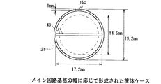
ところで、図31に示すように、例えば、14.5〔mm〕程度の外径を有する駆動用乾電池21と、17.2〔mm〕程度の幅を有するメイン回路基板43とを収納する筐体ケース150を、当該メイン回路基板43の幅に応じて円筒形状に形成すると、当該筐体ケース150の肉厚を1〔mm〕程度に選定しても、19.2〔mm〕程度の外径となる。
【0164】
これに対して、図32からも明らかなように、本実施の形態によるディジタル再生装置4では、駆動用乾電池21の外径に応じて筐体ケース10を形成することにより、筐体ケース10の肉厚を破損から保護し得るように選定し、かつ当該駆動用乾電池21と、筐体ケース10とのクリアランスを考慮しても、筐体ケース10の外径を17〔mm〕程度に選定することができる。
【0165】
そして、ディジタル再生装置4では、筐体ケース10にリブ35A及び35B並びに36A及び36Bにより、例えば4.5〔mm〕程度の幅を有する突出部を形成すれば、内部にメイン回路基板43を容易に収納することができ、かくして、メイン回路基板43の幅に応じて円筒形状に形成された筐体ケース150よりも格段的に小型化することができる。
【0166】
因みに、ディジタル再生装置4では、例えば、また当該筐体ケース10の対向する突出部を青色に塗装し、また、当該筐体ケース10の円筒状の部分を突出部よりも明るい銀色に塗装することにより、円筒状の部分を強調し、視覚的にも装置全体の小型化を強調することができる。
【0167】
以上の構成によれば、円筒形状の筐体ケース10の周側面にメイン回路基板43の幅方向の端部に応じた収納空間を有する突出部をケース長手方向に沿って対向させて設け、一方の突出部の内部から他方の突出部の内部に渡ってメイン回路基板43を収納するようにしたことにより、筐体ケース10の円筒形の形状を損なうことなく、当該円筒形の外径よりも幅広なメイン回路基板43を容易に収納することができ、かくして一段と小型化し得るディジタル再生装置を実現することができる。
【0168】
(4)他の実施の形態
なお上述の実施の形態においては、筐体ケース10の左右の側面にリブ35A及び35B並びに36A及び36Bにより、コ字状の突出部を設けるようにした場合について述べたが、本発明はこれに限らず、メイン回路基板43を収納することができれば、山状の突出部や、断面が水滴状となり筐体ケースに一体に形成された突出部等のように、この他種々の形状の突出部を設けるようにしても良い。
【0169】
また上述の実施の形態においては、筐体ケース10の左右の側面に突出部を設けるようにした場合について述べたが、本発明はこれに限らず、回路基板を収納することができれば、筐体ケース10の所定の1つの側面のみに突出部を設けたり、また回路基板の形状及び数に応じて2以上の突出部を種々の部位に設けるようにしても良い。
【0170】
さらに上述の実施の形態においては、所定の回路基板として、図15(A)及び(B)について上述したメイン回路基板43を適用するようにした場合について述べたが、本発明はこれに限らず、円盤状の回路基板や、サブ回路基板42と同様な台形状の回路基板等のように、この他種々の形状でなる回路基板に広く適用することができる。
【0171】
さらに上述の実施の形態においては、所定の内部空間を有する筐体ケースとして、ほぼ円筒状の筐体ケース10を適用するようにした場合について述べたが、本発明はこれに限らず、四角形の筒状のものや、箱状のもの等のように、この他種々の形状でなる筐体ケースを用いるようにしても良い。因みに、筐体ケースとして、例えば、薄型の箱状のものを用いる場合には、その一面及び又は他面に長手方向に沿って突出部を設ければ、回路基板を収納し得るのみならずに、当該筐体ケースの剛性を向上させることができる。
【0172】
さらに上述の実施の形態においては、筐体ケースに設けられ、内部空間から回路基板の突出する部分を、内部空間と一体化して収納するための収納空間が形成された内部空間拡張手段として、リブ35A及び35B並びに36A及び36Bを嵌合してなる突出部を適用するようにした場合について述べたが、本発明はこれに限らず、筐体ケースに設けられ、内部空間から回路基板の突出する部分を、内部空間と一体化して収納するための収納空間が形成されたものであれば、この他種々の形状及び構成でなる内部空間拡張手段を広く適用することができる。
【0173】
さらに上述の実施の形態においては、本発明による電子機器を図3について上述したディジタル再生装置4に適用するようにした場合について述べたが、本発明はこれに限らず、ディスク状記録媒体や、テープ状記録媒体を用いる記録及び又は再生装置、メモリーカードが着脱自在に装填される記録及び又は再生装置、ラジオ、また、携帯端末等のように、この他種々の電子機器に広く適用することができる。
【0174】
【発明の効果】
上述のように本発明によれば、円筒形状の筐体ケースと、筐体ケースの表面の所定部分に設けられた操作手段と、操作手段が操作されたときに当該操作手段と係合して操作信号を出力するための信号出力素子が配置され、当該信号出力素子が操作手段と対向して当該操作手段が操作されたときに係合するように、筐体ケース内に設けられた素子配置部材と、信号出力素子から出力される操作信号に基づいて所定の制御を行う制御素子が配置され、素子配置部材よりも筐体ケースの中心側に位置して素子配置部材が積層されるように筐体ケース内に設けられた回路基板とを設けるようにしたことにより、筐体ケースの形状を損なうことなく、回路基板を容易に収納することができ、かくして一段と小型化し得る電子機器を実現することができる。
【図面の簡単な説明】
【図1】ディジタル音楽コンテンツの利用形態の説明に供するブロック図である。
【図2】ディジタル音楽コンテンツの再生制限の説明に供する略線図である。
【図3】本実施の形態によるディジタル再生装置の構成を示す略線的斜視図である。
【図4】ディジタル再生装置の周側面の構成を示す左側面図、正面図、右側面図及び背面図である。
【図5】首掛け用のストラップが取り付けられたディジタル再生装置の説明に供する略線図である。
【図6】首掛け用のストラップが用いられて首からぶら下げられたディジタル再生装置の説明に供する略線図である。
【図7】ヘッドホンジャックへのプラグの差し込みの説明に供する略線的斜視図である。
【図8】胸ポケットに取り付けられたディジタル再生装置の説明に供する略線図である。
【図9】ディジタル再生装置の内部構成を示す略線的分解斜視図である。
【図10】乾電池収納部の構成を示す略線的断面図である。
【図11】シリアルラベルの構成を示す略線的斜視図及び略線的分解斜視図である。
【図12】表示部保護部材の構成を示す略線的斜視図である。
【図13】表示部の構成を示す略線的斜視図である。
【図14】サブ回路基板の構成を示す略線図正面図及び略線的背面図である。
【図15】メイン回路基板の構成を示す略線図正面図及び略線的背面図である。
【図16】サブ回路基板及びメイン回路基板の接続の説明に供する略線的側面図及び略線的上面図である。
【図17】正面側ケースへの表示部保護部材の取り付けの説明に供する略線的斜視図である。
【図18】表示部の取り付けの説明に供する略線的斜視図である。
【図19】筐体ケースへのメイン回路基板及びサブ回路基板の収納の説明に供する略線的斜視図である。
【図20】正面側ケースへの背面側ケースの取り付けの説明に供する略線的斜視図である。
【図21】正面側ケースへのサブ回路基板の収納の説明に供する略線的斜視図である。
【図22】筐体ケースへのメイン回路基板の収納の説明に供する略線的側面図である。
【図23】メイン回路基板への静電気の流れの説明に供する一部を断じた略線的断面図である。
【図24】表示部保護部材及びサブ回路基板の組み付けの説明に供する略線的側面図である。
【図25】表示部保護部材からサブ回路基板への静電気の流れの説明に供する一部を断じた略線的側面図である。
【図26】ディジタル再生装置の回路構成を示すブロック図である。
【図27】ディジタル音楽コンテンツのデータ構造を示す略線図である。
【図28】ヘッダのデータ構造(1)を示す略線図である。
【図29】ヘッダのデータ構造(2)を示す略線図である。
【図30】FATが格納された場合の半導体フラッシュメモリのデータ構造の説明に供する略線図である。
【図31】メイン回路基板の幅に応じて形成された筐体ケースの説明に供する略線的断面図である。
【図32】駆動用乾電池の外径に応じて形成された筐体ケースの説明に供する略線的断面図である。
【符号の説明】
4……ディジタル再生装置、10……筐体ケース、35……正面側ケース、35A、35B、36A、36B……リブ、35AX、35BX、36AX、36BX……嵌合部、36……背面側ケース、43……メイン回路基板。[0001]
BACKGROUND OF THE INVENTION
The present invention relates to an electronic device, and is suitable for application to, for example, a portable digital playback device capable of playing music data.
[0002]
[Prior art]
In recent years, as a portable digital playback device, a device using a semiconductor memory as music data storage means has been proposed, and music obtained by playing back music data from the semiconductor memory is enjoyed.
[0003]
[Problems to be solved by the invention]
By the way, in such a digital reproducing apparatus, further miniaturization is desired in order to improve portability.
[0004]
The present invention has been made in consideration of the above points, and intends to propose an electronic device that can be further miniaturized.
[0005]
[Means for Solving the Problems]
In order to solve this problem, in the present invention, Cylindrical shape Case case and case A predetermined part of the surface of Provided in Operating means When When the operation means is operated, a signal output element for engaging with the operation means and outputting an operation signal is disposed, and when the operation means is operated with the signal output element facing the operation means An element arrangement member provided in the housing case and a control element for performing predetermined control based on an operation signal output from the signal output element are arranged so as to engage with the housing, and the housing is arranged more than the element arrangement member. A circuit board provided in the housing case so that the element arrangement member is stacked on the center side of the case; It was made to provide.
[0006]
Therefore, the circuit board can be easily accommodated without impairing the shape of the housing case.
[0007]
DETAILED DESCRIPTION OF THE INVENTION
Hereinafter, an embodiment of the present invention will be described in detail with reference to the drawings.
[0008]
(1) Usage of electronic music distribution service
In recent years, an electronic music distribution service called EMD (Electric Music Distribution) that distributes digital music content using a computer network based on the Internet has been proposed.
[0009]
As shown in FIG. 1, in this type of electronic music distribution service, digital music is sent from an EMD
[0010]
In the
[0011]
In such an electronic music distribution service, there is a purchase method called “purchase” in which the digital music content C1 downloaded from the EMD
[0012]
Accordingly, when the user purchases the digital music content C1 from the EMD
[0013]
The
[0014]
As a result, the user can reproduce the digital music content C1 with “reproduction restriction” not only by the
[0015]
In practice, as shown in FIG. 2 (A), the digital music content C1 with “reproduction restriction” downloaded from the
[0016]
Next, as shown in FIG. 2B, the
[0017]
The
[0018]
By the way, in the digital reproducing
[0019]
In order to prevent such a situation, the
[0020]
However, as shown in FIG. 2C, the
[0021]
As a result, when the
[0022]
Further, when the
[0023]
In this way, the
[0024]
On the other hand, in the case of the digital music content C1 to which only the reproduction limit of the reproducible number of times is added, the
[0025]
(2) Overall configuration of digital playback device
(2-1) Structure of digital playback device
As shown in FIG. 3, the
[0026]
Here, when the side on which the
[0027]
As shown in FIG. 4A, on the left side surface of the
[0028]
Actually, the
[0029]
Further, as shown in FIG. 4B, the volume up
[0030]
Then, on the front surface of the
[0031]
Incidentally, the
[0032]
Further, as shown in FIG. 4C, a
[0033]
In addition to this, as shown in FIG. 4 (D), on the rear surface of the
[0034]
Thereby, in the dry
[0035]
In addition, on the rear surface of the
[0036]
The strap metal fitting 27 is configured to be freely rotatable within a range of approximately 180 degrees from the posture in contact with the
[0037]
Here, in the
[0038]
For this reason, as shown in FIG. 5, the
[0039]
By the way, the digital reproducing
[0040]
In the digital reproducing
[0041]
Thus, in the
[0042]
Incidentally, in the digital reproducing
[0043]
Further, in the digital reproducing
[0044]
Therefore, in the digital reproducing
[0045]
In addition to this, in the digital reproducing
[0046]
Thus, in the
[0047]
In the
[0048]
Here, in the
[0049]
The
[0050]
And the
[0051]
Actually, as shown in FIGS. 10A and 10B, the dry
[0052]
In this case, in the dry
[0053]
A
[0054]
Further, a sheet-like serial label 48 having a thickness of about 0.1 mm is attached to the bottom of the dry
[0055]
As shown in FIGS. 11A and 11B, the serial label 48 is made of, for example, an acrylic pressure-
[0056]
Incidentally, in the serial label 48, a
[0057]
Therefore, in the dry cell storage unit 22 (FIGS. 10A and 10B), the conductive plate 47 is lifted from the
[0058]
In the dry
[0059]
Moreover, in the dry
[0060]
On the other hand, as shown in FIG. 12, the display
[0061]
Further, in the
[0062]
In the
[0063]
In addition, the
[0064]
As shown in FIG. 14A, the
[0065]
Also, a plurality of LCD lands 71 made of a conductor pattern are formed on one surface of the
[0066]
Further, as shown in FIG. 14B, on the other surface of the
[0067]
Incidentally, on the other surface of the
[0068]
As shown in FIG. 15A, the
[0069]
As shown in FIG. 15B, on the other side of the
[0070]
As shown in FIGS. 16A and 16B, in the
[0071]
Incidentally, a bus is formed by a conductor pattern on the
[0072]
Further, the surface-mounted electronic components are mounted on one surface of the
[0073]
By the way, in the main circuit board 43 (FIG. 15A), after the female-type board-to-
[0074]
Similarly, in the sub circuit board 42 (FIG. 14B), after the male
[0075]
For this reason, the sub circuit board 42 (FIG. 16B), when connected to the
[0076]
A board-to-
[0077]
However, the
[0078]
Actually, in the front case 35 (FIG. 9), a
[0079]
In addition to this, in the display part protection member 40 (FIG. 12), a
[0080]
Accordingly, in the
[0081]
In the
[0082]
In the
[0083]
Next, as shown in FIG. 20, the
[0084]
By the way, as the
[0085]
Therefore, the board-to-
[0086]
However, in the board-to-
[0087]
Therefore, in the board-to-
[0088]
Accordingly, as shown in FIG. 21, even if the
[0089]
Thus, in the
[0090]
Further, in the digital reproducing
[0091]
Incidentally, in the
[0092]
The
[0093]
Further, in the sub circuit board 42 (FIG. 14A), the LCD lands 71 are formed to have a predetermined length along the width direction of the
[0094]
The
[0095]
Therefore, as shown in FIG. 22, L-shaped
[0096]
The
[0097]
As a result, in the
[0098]
Further, in the
[0099]
By the way, on the other surface of the main circuit board 43 (FIG. 15B), a conductor pattern for ground (hereinafter referred to as a ground pattern) is formed at both ends in the width direction from one end to the other end in the longitudinal direction. 92) is formed, and the
[0100]
As a result, as shown in FIG. 23, when the
[0101]
Moreover, in the display part protection member 40 (FIG. 12), it consists of an electroconductive metal plate as mentioned above, and the
[0102]
In addition, a
[0103]
As shown in FIGS. 24 and 25, in the display
[0104]
As a result, when the
[0105]
In addition to this, in the display
[0106]
Further, since the display
[0107]
(2-2) Circuit configuration of digital reproduction device
Next, the circuit configuration of the digital reproducing
[0108]
When the
[0109]
Here, the digital music content C1 has a frame structure of 64 [Bytes] per packet, and is transferred from the
[0110]
The digital music content C1 includes a header H1 and music data D1, as shown in FIG. 27. The header H1 includes “file ID”, “header size”, “content key (for encryption)”, “file size”. ”,“ Codec ID ”,“ File name ”, and“ File information ”are stored, and“ Reproduction restriction data ”,“ Reproduction start date ”, and“ Reproduction end date ”are included as reproduction restriction information necessary for the reproduction restriction process. , “Reproducible number of times” and “actual number of times of reproduction” are stored.
[0111]
Actually, in the header H1, as shown in FIG. 28 showing the stored information in hexadecimal notation, the “header size” represents the data length of the header H1 (33 bytes in this case). "Represents the data length of the file of the music data D1 (in this case, 3636138 bytes).
[0112]
The “content key” is encrypted data for decrypting the music data D1 (FIG. 27), and when the digital music content C1 is actually exchanged between the
[0113]
Actually, when the
[0114]
Here, the challenge-response method responds to a value (challenge) generated by the
[0115]
The “codec ID” is an ID number corresponding to the decompression method when the
[0116]
The “file name” is data obtained by converting, for example, the file name “ABCD.AC” of the digital music content C1 into an ASCII (American National Standard Code for Information Interchange) code, and the “file information” is the digital music content C1. This is data obtained by converting a song name, artist name, composer name, composer name, etc. into ASCII code.
[0117]
“Reproduction restriction data” is data indicating whether or not the reproduction limitation of the reproducible period or the reproducible number of times is added to the digital music content C1 reproduced by the
[0118]
The “reproduction start date” and “reproduction end date” are data indicating the range of the reproducible period when the “reproduction restriction data” is “2”, and “0640F” and “000000F” indicate “ “April 15, 2000” to “July 15, 2000” indicates the range of the reproducible period.
[0119]
Similarly, the “reproducible number of times” and “actual number of times of reproduction” are the maximum number of reproducible times specified in advance when “reproduction restriction data” is “1” and “2”, and the reproduction process is executed. Is the data indicating the actual number of reproductions updated by the
[0120]
Therefore, according to the reproduction restriction information in the header H1, as described above with reference to FIG. 2, the
[0121]
Incidentally, the header H1 of the digital music content C1 to which playback restriction is added only to the number of playbacks possible, for example, as shown in FIG. 29, “playback restriction data” indicates “1”, “playback start date” and “playback end”. “Day” is “000000” and “000000”, and “Number of reproducible times” and “Number of actual times of reproduction” are “0a” and “05”. That is, there is no restriction on the reproducible period by the “reproduction start date” and the “reproduction end date”, the “reproducible number” is “10” times, and the current “actual reproduction number” is “5” Show.
[0122]
By the way, in the digital reproduction device 4 (FIG. 26), a writing instruction for the digital music content C1 is transferred together with the digital music content C1 from the
[0123]
Incidentally, the
[0124]
The
[0125]
Accordingly, when a playback command corresponding to the user's pressing operation of the playback /
[0126]
The
[0127]
Here, the
[0128]
In this case, the
[0129]
Similarly,
[0130]
This eliminates the need for a clock generation module for supplying a clock to each circuit block such as the
[0131]
The digital-
[0132]
As described above, when the play /
[0133]
Further, when the playback /
[0134]
Incidentally, even if the playback /
[0135]
In addition, the
[0136]
Furthermore, in the
[0137]
Incidentally, in this embodiment, 64 [KBByte] of the digital music content C1 is handled as one block, and the block position corresponding to one piece of digital music content C1 is included in the FAT.
[0138]
When the FAT is stored in the
[0139]
Thus, since the FAT is rewritten every time the digital music content C1 is written to the
[0140]
In addition, the FAT is configured so that the same data is written twice for reserve, and even if the driving
[0141]
However, although the
[0142]
For this reason, when the FAT is stored in the
[0143]
That is, if the
[0144]
On the other hand, the
[0145]
As described above, the
[0146]
In practice, the
[0147]
Further, the
[0148]
By the way, when the
[0149]
When the
[0150]
At this time, the
[0151]
As described above, when the USB connection is established, the
[0152]
The
[0153]
When the
[0154]
At the same time, the
[0155]
As a result, the
[0156]
At this time, the
[0157]
(3) Operation and effect of the present embodiment
In the above configuration, in the digital reproducing
[0158]
In the
[0159]
Accordingly, in the
[0160]
Further, in the digital reproducing
[0161]
In addition to this, in the digital reproducing
[0162]
As a result, in the
[0163]
By the way, as shown in FIG. 31, for example, a housing for storing a driving
[0164]
On the other hand, as is clear from FIG. 32, in the
[0165]
In the digital reproducing
[0166]
Incidentally, in the digital reproducing
[0167]
According to the above configuration, the protruding portion having the storage space corresponding to the end portion in the width direction of the
[0168]
(4) Other embodiments
In the above-described embodiment, the case where the U-shaped protrusions are provided by the
[0169]
Moreover, in the above-described embodiment, the case where the protrusions are provided on the left and right side surfaces of the
[0170]
Furthermore, in the above-described embodiment, the case where the
[0171]
Furthermore, in the above-described embodiment, the case where the substantially
[0172]
Furthermore, in the above-described embodiment, ribs are provided as internal space expansion means provided in the housing case and formed with a storage space for storing a portion of the circuit board protruding from the internal space so as to be integrated with the internal space. Although the case where the projection part formed by fitting 35A and 35B and 36A and 36B is applied is described, the present invention is not limited to this, and the circuit board is provided from the internal space and protrudes from the internal space. As long as a storage space for storing the part in an integrated manner with the internal space is formed, internal space expansion means having various shapes and configurations can be widely applied.
[0173]
Furthermore, in the above-described embodiment, the case where the electronic apparatus according to the present invention is applied to the
[0174]
【The invention's effect】
As described above, according to the present invention, Cylindrical shape Case case and case A predetermined part of the surface of Provided in Operating means When When the operation means is operated, a signal output element for engaging with the operation means and outputting an operation signal is disposed, and when the operation means is operated with the signal output element facing the operation means An element arrangement member provided in the housing case and a control element for performing predetermined control based on an operation signal output from the signal output element are arranged so as to engage with the housing, and the housing is arranged more than the element arrangement member. A circuit board provided in the housing case so that the element arrangement member is stacked on the center side of the case; By providing the circuit board, it is possible to easily store the circuit board without impairing the shape of the housing case, and thus it is possible to realize an electronic device that can be further downsized.
[Brief description of the drawings]
FIG. 1 is a block diagram for explaining a usage form of digital music content.
FIG. 2 is a schematic diagram for explaining the restriction on reproduction of digital music content.
FIG. 3 is a schematic perspective view showing a configuration of a digital reproducing apparatus according to the present embodiment.
FIGS. 4A and 4B are a left side view, a front view, a right side view, and a rear view showing the configuration of the peripheral side surface of the digital playback device. FIGS.
FIG. 5 is a schematic diagram for explaining a digital reproduction apparatus to which a strap for hanging around a neck is attached.
FIG. 6 is a schematic diagram for explaining a digital reproducing apparatus that is hung from a neck using a strap for hanging around the neck.
FIG. 7 is a schematic perspective view for explaining the insertion of the plug into the headphone jack.
FIG. 8 is a schematic diagram for explaining a digital reproduction device attached to a breast pocket.
FIG. 9 is a schematic exploded perspective view showing the internal structure of the digital playback device.
FIG. 10 is a schematic cross-sectional view showing a configuration of a dry cell storage unit.
FIG. 11 is a schematic perspective view and a schematic exploded perspective view showing the configuration of a serial label.
FIG. 12 is a schematic perspective view illustrating a configuration of a display unit protection member.
FIG. 13 is a schematic perspective view showing a configuration of a display unit.
FIGS. 14A and 14B are a schematic diagram front view and a schematic rear view showing a configuration of a sub circuit board, respectively.
FIG. 15 is a schematic diagram front view and a schematic diagram rear view showing the configuration of the main circuit board;
FIG. 16 is a schematic side view and a schematic top view for explaining the connection between the sub circuit board and the main circuit board;
FIG. 17 is a schematic perspective view for explaining the attachment of the display unit protection member to the front case.
FIG. 18 is a schematic perspective view for explaining attachment of a display unit.
FIG. 19 is a schematic perspective view for explaining the storage of the main circuit board and the sub circuit board in the housing case.
FIG. 20 is a schematic perspective view for explaining the attachment of the rear case to the front case.
FIG. 21 is a schematic perspective view for explaining the storage of the sub circuit board in the front case.
FIG. 22 is a schematic side view for explaining the storage of the main circuit board in the housing case.
FIG. 23 is a schematic cross-sectional view with a part cut away for explaining the flow of static electricity to the main circuit board;
FIG. 24 is a schematic side view for explaining the assembly of the display unit protection member and the sub circuit board.
FIG. 25 is a schematic side view with a part cut away for explaining the flow of static electricity from the display unit protection member to the sub circuit board;
FIG. 26 is a block diagram illustrating a circuit configuration of a digital reproduction device.
FIG. 27 is a schematic diagram illustrating a data structure of digital music content.
FIG. 28 is a schematic diagram illustrating a data structure (1) of a header.
FIG. 29 is a schematic diagram illustrating a data structure (2) of a header.
FIG. 30 is a schematic diagram for explaining a data structure of a semiconductor flash memory when FAT is stored;
FIG. 31 is a schematic cross-sectional view for explaining a casing case formed according to the width of the main circuit board.
FIG. 32 is a schematic cross-sectional view for explaining a housing case formed according to the outer diameter of the driving dry battery.
[Explanation of symbols]
4. Digital reproduction device, 10 ... Housing case, 35 ... Front side case, 35A, 35B, 36A, 36B ... Rib, 35AX, 35BX, 36AX, 36BX ... Fitting part, 36 ... Back side Case, 43 …… Main circuit board.
Claims (6)
上記筐体ケースの表面の所定部分に設けられた操作手段と、
上記操作手段が操作されたときに当該操作手段と係合して操作信号を出力するための信号出力素子が配置され、当該信号出力素子が上記操作手段と対向して当該操作手段が操作されたときに係合するように、上記筐体ケース内に設けられた素子配置部材と、
上記信号出力素子から出力される上記操作信号に基づいて所定の制御を行う制御素子が配置され、上記素子配置部材よりも上記筐体ケースの中心側に位置して上記素子配置部材が積層されるように上記筐体ケース内に設けられた回路基板と
を具える電子機器。 A cylindrical housing case;
Operating means provided on a predetermined portion of the surface of the housing case ;
When the operation means is operated, a signal output element for engaging with the operation means and outputting an operation signal is disposed, and the operation means is operated with the signal output element facing the operation means. An element arrangement member provided in the housing case so as to be sometimes engaged;
A control element that performs predetermined control based on the operation signal output from the signal output element is disposed, and the element disposition member is stacked at a position closer to the center of the housing case than the element disposition member. the housing a circuit board and Ru electronic device comprising a provided in the case so as.
を具える請求項1に記載の電子機器。 In the upper Kikatamitai case, the display means provided in contact with said element mounting member
The electronic device according to claim 1, comprising:
上記表示手段は、上記素子配置部材の上記開口部と対向して、当該素子配置部材の上記信号出力素子が配置された一面の裏となる他面側に設けられた
請求項2に記載の電子機器。 The element arrangement member is provided with an opening corresponding to the display means,
The said display means was provided in the other surface side which becomes the back of one surface where the said signal output element of the said element arrangement | positioning member was arrange | positioned facing the said opening part of the said element arrangement | positioning member.
The electronic device according to 請 Motomeko 2.
上記他の操作手段が操作されたときに当該他の操作手段と係合して操作信号を出力するための他の信号出力素子が配置され、上記素子配置部材と上記回路基板との間に介在するように上記筐体ケース内に設けられた他の回路基板と
を具える請求項3に記載の電子機器。 Other operating means provided on the end surface of the casing case ,
When the other operation means is operated, another signal output element for engaging with the other operation means and outputting an operation signal is arranged, and interposed between the element arrangement member and the circuit board. And other circuit boards provided in the housing case
The electronic device according to claim 3, comprising:
上記スライドスイッチが操作されたときに当該スライドスイッチと係合して操作信号を出力するためのスイッチ回路素子が配置され、上記スイッチ回路素子が上記スライドスイッチと対向して当該スライドスイッチが操作されたときに係合するように、上記筐体ケース内に設けられたスイッチ回路基板と
を具える請求項4に記載の電子機器。 A slide switch slidably provided on a predetermined portion on the other surface side of the element arrangement member with respect to the surface of the housing case;
When the slide switch is operated, a switch circuit element for engaging with the slide switch and outputting an operation signal is disposed, and the switch circuit element is opposed to the slide switch and the slide switch is operated. A switch circuit board provided in the housing case so as to be engaged sometimes
The electronic device according to claim 4 comprising:
請求項5に記載の電子機器。 The element arrangement member is formed by bending both ends of the metal plate, and the signal output element is arranged on a flat plate portion between the bent both ends.
The electronic device according to 請 Motomeko 5.
Priority Applications (2)
| Application Number | Priority Date | Filing Date | Title |
|---|---|---|---|
| JP36144399A JP4232065B2 (en) | 1999-11-14 | 1999-11-14 | Electronics |
| TW89123880A TW487868B (en) | 1999-11-14 | 2000-11-10 | Portable record and/or reproduce device, method of reproducing, and method of recording and reproducing |
Applications Claiming Priority (1)
| Application Number | Priority Date | Filing Date | Title |
|---|---|---|---|
| JP36144399A JP4232065B2 (en) | 1999-11-14 | 1999-11-14 | Electronics |
Publications (3)
| Publication Number | Publication Date |
|---|---|
| JP2001144470A JP2001144470A (en) | 2001-05-25 |
| JP2001144470A5 JP2001144470A5 (en) | 2006-05-11 |
| JP4232065B2 true JP4232065B2 (en) | 2009-03-04 |
Family
ID=18473608
Family Applications (1)
| Application Number | Title | Priority Date | Filing Date |
|---|---|---|---|
| JP36144399A Expired - Lifetime JP4232065B2 (en) | 1999-11-14 | 1999-11-14 | Electronics |
Country Status (1)
| Country | Link |
|---|---|
| JP (1) | JP4232065B2 (en) |
Families Citing this family (2)
| Publication number | Priority date | Publication date | Assignee | Title |
|---|---|---|---|---|
| JP2007025988A (en) * | 2005-07-14 | 2007-02-01 | Kenwood Corp | Portable music appliance, power source control method and program |
| CN113138632A (en) | 2020-01-16 | 2021-07-20 | 华为技术有限公司 | Case and storage device |
-
1999
- 1999-11-14 JP JP36144399A patent/JP4232065B2/en not_active Expired - Lifetime
Also Published As
| Publication number | Publication date |
|---|---|
| JP2001144470A (en) | 2001-05-25 |
Similar Documents
| Publication | Publication Date | Title |
|---|---|---|
| JP4304558B2 (en) | Portable device | |
| US6976111B1 (en) | High-density removable expansion module having I/O and second-level removable expansion memory | |
| EP0689127B1 (en) | Recording and/or reproducing system and data backup system | |
| WO2001098879A1 (en) | Portable terminal equipped with a recording medium | |
| KR20010067408A (en) | A data reproducing apparatus | |
| KR100788045B1 (en) | Reproduction apparatus and reproduction method | |
| US20060232922A1 (en) | Portable digital storage device | |
| JP4232065B2 (en) | Electronics | |
| JP3519988B2 (en) | Battery insulation / display surface protection sheet and portable information terminal with battery insulation / display surface protection sheet | |
| JP2001142474A (en) | Data reproducing device, clock supply control method and program storage medium | |
| JP2001143674A (en) | Electronic equipment and battery housing device | |
| JP2001142580A (en) | Data reproducing device, power supplying method and program storing medium | |
| JP2001144469A (en) | Electronic apparatus | |
| JP2001143481A (en) | Data recording/reproducing apparatus | |
| JP2001144468A (en) | Electronic apparatus | |
| JP2001197659A (en) | Current route cut-off circuit and data regenerating apparatus | |
| JP2001144467A (en) | Electronic apparatus | |
| JP2001197681A (en) | Power supply switching circuit and data reproducing apparatus | |
| US20060075151A1 (en) | Mp3 walkman with a replaceable hard disk | |
| JP2816318B2 (en) | Electronics | |
| TW487868B (en) | Portable record and/or reproduce device, method of reproducing, and method of recording and reproducing | |
| WO1999041679A1 (en) | Portable electronic appliance | |
| KR200167123Y1 (en) | MP3 player which can connect with patable phone | |
| JP2001357359A (en) | Ic card recorder and/or reproducer | |
| KR20090011227A (en) | Portable media terminal |
Legal Events
| Date | Code | Title | Description |
|---|---|---|---|
| A521 | Written amendment |
Free format text: JAPANESE INTERMEDIATE CODE: A523 Effective date: 20060310 |
|
| A621 | Written request for application examination |
Free format text: JAPANESE INTERMEDIATE CODE: A621 Effective date: 20060310 |
|
| A521 | Written amendment |
Free format text: JAPANESE INTERMEDIATE CODE: A523 Effective date: 20060501 |
|
| A977 | Report on retrieval |
Free format text: JAPANESE INTERMEDIATE CODE: A971007 Effective date: 20080820 |
|
| A131 | Notification of reasons for refusal |
Free format text: JAPANESE INTERMEDIATE CODE: A131 Effective date: 20080828 |
|
| A521 | Written amendment |
Free format text: JAPANESE INTERMEDIATE CODE: A523 Effective date: 20081020 |
|
| TRDD | Decision of grant or rejection written | ||
| A01 | Written decision to grant a patent or to grant a registration (utility model) |
Free format text: JAPANESE INTERMEDIATE CODE: A01 Effective date: 20081113 |
|
| A01 | Written decision to grant a patent or to grant a registration (utility model) |
Free format text: JAPANESE INTERMEDIATE CODE: A01 |
|
| A61 | First payment of annual fees (during grant procedure) |
Free format text: JAPANESE INTERMEDIATE CODE: A61 Effective date: 20081126 |
|
| FPAY | Renewal fee payment (event date is renewal date of database) |
Free format text: PAYMENT UNTIL: 20111219 Year of fee payment: 3 |
|
| R151 | Written notification of patent or utility model registration |
Ref document number: 4232065 Country of ref document: JP Free format text: JAPANESE INTERMEDIATE CODE: R151 |
|
| FPAY | Renewal fee payment (event date is renewal date of database) |
Free format text: PAYMENT UNTIL: 20111219 Year of fee payment: 3 |
|
| FPAY | Renewal fee payment (event date is renewal date of database) |
Free format text: PAYMENT UNTIL: 20121219 Year of fee payment: 4 |
|
| R250 | Receipt of annual fees |
Free format text: JAPANESE INTERMEDIATE CODE: R250 |
|
| FPAY | Renewal fee payment (event date is renewal date of database) |
Free format text: PAYMENT UNTIL: 20121219 Year of fee payment: 4 |
|
| FPAY | Renewal fee payment (event date is renewal date of database) |
Free format text: PAYMENT UNTIL: 20131219 Year of fee payment: 5 |
|
| R250 | Receipt of annual fees |
Free format text: JAPANESE INTERMEDIATE CODE: R250 |
|
| R250 | Receipt of annual fees |
Free format text: JAPANESE INTERMEDIATE CODE: R250 |
|
| R250 | Receipt of annual fees |
Free format text: JAPANESE INTERMEDIATE CODE: R250 |
|
| R250 | Receipt of annual fees |
Free format text: JAPANESE INTERMEDIATE CODE: R250 |
|
| R250 | Receipt of annual fees |
Free format text: JAPANESE INTERMEDIATE CODE: R250 |
|
| R250 | Receipt of annual fees |
Free format text: JAPANESE INTERMEDIATE CODE: R250 |
|
| R250 | Receipt of annual fees |
Free format text: JAPANESE INTERMEDIATE CODE: R250 |
|
| EXPY | Cancellation because of completion of term |