JP4231663B2 - Semiconductor device - Google Patents
Semiconductor device Download PDFInfo
- Publication number
- JP4231663B2 JP4231663B2 JP2002165554A JP2002165554A JP4231663B2 JP 4231663 B2 JP4231663 B2 JP 4231663B2 JP 2002165554 A JP2002165554 A JP 2002165554A JP 2002165554 A JP2002165554 A JP 2002165554A JP 4231663 B2 JP4231663 B2 JP 4231663B2
- Authority
- JP
- Japan
- Prior art keywords
- wiring
- semiconductor device
- region
- layer wiring
- semiconductor
- Prior art date
- Legal status (The legal status is an assumption and is not a legal conclusion. Google has not performed a legal analysis and makes no representation as to the accuracy of the status listed.)
- Expired - Fee Related
Links
Images


Classifications
-
- H—ELECTRICITY
- H10—SEMICONDUCTOR DEVICES; ELECTRIC SOLID-STATE DEVICES NOT OTHERWISE PROVIDED FOR
- H10W—GENERIC PACKAGES, INTERCONNECTIONS, CONNECTORS OR OTHER CONSTRUCTIONAL DETAILS OF DEVICES COVERED BY CLASS H10
- H10W72/00—Interconnections or connectors in packages
- H10W72/90—Bond pads, in general
-
- H—ELECTRICITY
- H10—SEMICONDUCTOR DEVICES; ELECTRIC SOLID-STATE DEVICES NOT OTHERWISE PROVIDED FOR
- H10W—GENERIC PACKAGES, INTERCONNECTIONS, CONNECTORS OR OTHER CONSTRUCTIONAL DETAILS OF DEVICES COVERED BY CLASS H10
- H10W72/00—Interconnections or connectors in packages
- H10W72/50—Bond wires
- H10W72/59—Bond pads specially adapted therefor
-
- H—ELECTRICITY
- H10—SEMICONDUCTOR DEVICES; ELECTRIC SOLID-STATE DEVICES NOT OTHERWISE PROVIDED FOR
- H10W—GENERIC PACKAGES, INTERCONNECTIONS, CONNECTORS OR OTHER CONSTRUCTIONAL DETAILS OF DEVICES COVERED BY CLASS H10
- H10W72/00—Interconnections or connectors in packages
- H10W72/90—Bond pads, in general
- H10W72/931—Shapes of bond pads
- H10W72/932—Plan-view shape, i.e. in top view
-
- H—ELECTRICITY
- H10—SEMICONDUCTOR DEVICES; ELECTRIC SOLID-STATE DEVICES NOT OTHERWISE PROVIDED FOR
- H10W—GENERIC PACKAGES, INTERCONNECTIONS, CONNECTORS OR OTHER CONSTRUCTIONAL DETAILS OF DEVICES COVERED BY CLASS H10
- H10W72/00—Interconnections or connectors in packages
- H10W72/90—Bond pads, in general
- H10W72/981—Auxiliary members, e.g. spacers
- H10W72/983—Reinforcing structures, e.g. collars
Landscapes
- Semiconductor Integrated Circuits (AREA)
- Design And Manufacture Of Integrated Circuits (AREA)
Abstract
Description
【0001】
【発明の属する技術分野】
本発明は、半導体装置に関し、特に、高周波での信号伝送および広帯域での高速な信号伝送が要求される半導体装置に適用して有効な技術に関するものである。
【0002】
【従来の技術】
たとえば光通信用ICのような高速LSIが形成された半導体チップを搭載するパッケージに対しては、DCから実際に使用される高周波帯域までの広帯域の信号伝送が要求されている。特に、10Gbit/sec以上のビットレートにおいて、前記パッケージに対しては、高周波でのインピーダンス整合および低損失が要求されている。このような要求に対する対策として、信号伝送線路を形成したパッケージ基板の主面上に半導体チップをフェイスダウン方式で実装し、信号伝送線路の一端を半導体チップの主面に形成した電極パッドの直下まで延在することによって、信号伝送線路と電極パッドとがバンプ電極を介して電気的に接続するように実装する手段が考えられる。この手段によれば、信号伝送線路と半導体チップとを最短距離で接続することができるので、信号伝送線路から半導体チップの電極パッドに到るまでの伝送特性を良好に保存することができる。パッケージング材料としてセラミックを用いることにより、低損失でインピーダンス整合のとれた伝送線を形成することができる。また、パッケージング材料としてセラミックを用いて気密封止することによって半導体チップを外部環境から保護し、機械的強度、耐湿性、耐熱性および放熱性などに優れるパッケージを実現することができる。
【0003】
たとえば特開平7−147352号公報では、パッケージ基板上に形成された信号伝送線路の配線幅を半導体チップと重なる領域で狭くし、半導体チップと信号伝送線路との間に形成される容量に起因するインピーダンスの低下を補償することによって、パッケージ内の信号伝送線路の特性インピーダンス整合を図る技術について開示されている。また、セラミックから形成されたパッケージ基板を用いることにより、パッケージにおける伝送信号の損失を低減する技術についても開示されている。
【0004】
【発明が解決しようとする課題】
上記したようなパッケージ基板の主面上に半導体チップをフェイスダウン方式で実装する場合には、半導体チップの主面に形成した電極パッド上にバンプ電極(はんだボール)を形成する必要がある。このバンプ電極は、たとえば個々の半導体チップに切断する前の半導体ウェハの主面にフォトレジスト膜を形成およびパターニングした後、めっき法などを用いて電極パッド上に形成することになる。そのため、たとえば電極パッドとパッケージ基板とをワイヤボンディングすることで実装する手段に比べて、半導体ウェハに対しての処理工程数が増加してしまうこととなり、半導体ウェハの製造コストが高価になってしまうことになる。
【0005】
また、半導体チップをフェイスダウン方式で実装することから、実装工程時においては、バンプ電極とパッケージ基板との接続部分が視認できなくなる。そのため、たとえばワイヤボンディング法によって半導体チップをパッケージ基板に実装する場合に比べて実装が困難になってしまうことから、パッケージの製造コストが高価になってしまうことになる。
【0006】
また、パッケージング材料としてセラミックを用いた場合には、たとえばプラスチックを用いた場合に比べて材料コストが高くなることから、パッケージの製造コストが高価になってしまうことになる。
【0007】
そこで、本発明者は、ワイヤボンディング法およびエポキシ樹脂などのプラスチックをパッケージング材料としたパッケージング法を用い、高速LSIが形成された半導体チップを搭載するパッケージを形成する手段について検討している。その中で、本発明者は以下のような課題を見出した。
【0008】
すなわち、ワイヤボンディング法を用いることによって、ボンディングワイヤ部においてインピーダンスが増加することから、信号伝送線路から半導体チップの電極パッドに到るまでの伝送特性を良好に保存することができなくなってしまう問題が存在する。
【0009】
本発明の目的は、ワイヤボンディング法を用い、高速LSIが形成された半導体チップを搭載するパッケージを形成する手段を提供することにある。
【0010】
本発明の前記ならびにその他の目的と新規な特徴は、本明細書の記述および添付図面から明らかになるであろう。
【0011】
【課題を解決するための手段】
本願において開示される発明のうち、代表的なものの概要を簡単に説明すれば、次のとおりである。
【0012】
すなわち、本発明は、半導体基板上に形成され、接地電位と電気的に接続された第1配線と、前記第1配線上に形成された第1絶縁膜と、前記第1絶縁膜上に形成され、信号伝送線路である第2配線とを有し、前記第2配線は第1領域と第2領域と第3領域とを含み、前記第2配線の前記第1領域にはボンディングワイヤが接続され、前記第2配線の前記第2領域における配線幅は前記第3領域における配線幅よりも大きいものである。
【0013】
【発明の実施の形態】
以下、本発明の実施の形態を図面に基づいて詳細に説明する。なお、実施の形態を説明するための全図において、同一の機能を有する部材には同一の符号を付し、その繰り返しの説明は省略する。また、以下の実施の形態の説明に用いる図面においては、図面をわかりやすくするために平面図であってもハッチングを付す場合がある。
【0014】
(実施の形態1)
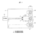
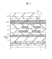
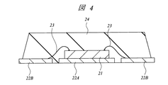
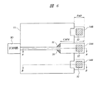
本実施の形態1の半導体装置は、たとえば光通信用IC(高速LSI)が形成された半導体チップを搭載するパッケージである。図1は本実施の形態1の半導体装置の要部平面図であり、図2は図1中のA−A線に沿った断面図であり、図3は図1中のB−B線に沿った断面図であり、図4は本実施の形態1の半導体装置の要部断面図である。
【0015】
図2および図3に示すように、本実施の形態1の半導体装置は、たとえば半導体素子が形成されるボンド基板となる単結晶シリコン(SOI(Silicon On Insulator)層)とベース基板となる単結晶シリコンとを酸化膜(BOX(Buried Oxide)層)を介して接着した後、ボンド基板を薄膜化することによって形成した半導体基板1を用いて形成される。図2および図3中での図示を省略したI/O(Input/Output)回路(第1回路)IO(図1参照)が形成される領域において、半導体基板1のSOI層には、たとえばnpn型バイポーラトランジスタおよびpnp型バイポーラトランジスタのうちの少なくとも一方が形成されている。
【0016】
半導体基板1上には、下層から順に第1層配線(第1配線)11を含む配線層(第1配線層)、第2層配線12を含む配線層、第3層配線13を含む配線層および第4層配線14A、14Bを含む配線層(第2配線層)が形成されている。これらの配線は、たとえばTi(チタン)膜、TiN(窒化チタン)膜およびTi膜を積層してなるバリア導体膜と、主導電層となるAl(アルミニウム)合金膜と、Ti膜およびTiN膜を積層してなるバリア導体膜との積層膜をパターニングすることで形成することができる。最上層配線となる第4層配線14A、14Bの主導電層のAl合金膜は、他の配線の主導電層のAl合金膜より相対的に厚い膜厚で形成されている。また、第1層配線11と半導体基板1との間および各配線間には、たとえば酸化シリコンからなる層間絶縁膜(第1絶縁膜)15が形成されている。第4層配線14Aを除く各配線間は、プラグ17を介して電気的に接続されている。このプラグ17は、たとえば層間絶縁膜15に形成した孔部内にTi膜とTiN膜とからなる積層膜およびW膜を順次堆積した後、その孔部の外部の積層膜およびW膜を除去することによって形成することができる。
【0017】
第4層配線(第2配線)14Aは、信号伝送線であり、I/O回路19と電気的に接続されている。また、第4層配線14Aおよび第1層配線11は、その間に誘電体(層間絶縁膜15)を挟むことにより、いわゆるマイクロストリップ線路(構造)を形成している。第4層配線14Bは、第3層配線13、第2層配線12および第1層配線11を介して接地(基準)電位(GND)と電気的に接続されている。また、第4層配線14A、14Bの端部の領域(パッド領域)PAD(図1参照)は、ワイヤボンディングのためのボンディングパッドとなっている。第4層配線14A、14Bの上部には、下層から酸化シリコン膜、窒化シリコン膜およびポリイミド膜を積層してなる保護膜18が形成されている。この保護膜18には、前記ボンディングパッド上において開口部19が形成されている。
【0018】
図4に示すように、本実施の形態1の光通信用ICが形成された半導体チップ21は、たとえばリードフレームのダイパッド22Aに接着され、第4層配線14A、14Bの端部の領域PAD(図1参照)とアウターリード22BとがAu(金)からなるワイヤ23によってワイヤボンディングされ、エポキシ樹脂24によって封止されることによってパッケージングされている。エポキシ樹脂24のようなプラスチックをパッケージング材料として用いることにより、たとえばセラミックをパッケージング材料として用いた場合よりも相対的にパッケージの製造コストを低減することができる。
【0019】
ところで、本実施の形態1のパッケージにおける線路インピーダンスZは、インダクタンスをLとし容量をCとすると、簡易的にZ=(L/C)1/2と表すことができる。線路インピーダンスZは、パッケージ内の信号伝送線路の特性インピーダンス整合を図るために、たとえば50Ωというように所定の値(第1の値)で規定される。上記したように、本実施の形態1においては、半導体チップ21とリードフレームとをワイヤボンディングする手段が用いられている。そのため、ワイヤ23におけるインダクタンス成分が加わることにより、線路インピーダンスZが変動してしまうことになる。そこで、本実施の形態1では、第4層配線14Aについて、領域PADを含む端部からの領域(第1領域)CAPAをI/O回路IOに向かって延在する領域(第3領域)に比べて配線幅を広く形成する。ここで、本実施の形態において、配線幅とは、配線の延在方向と直交する方向における配線の大きさのことを示すものとする。そして、第4層配線14Aの領域CAPAおよび第1層配線11を容量電極とし、第1層配線11と第4層配線14Aとの間の3層の層間絶縁膜15を容量絶縁膜とするキャパシタを形成する。また、第4層配線14Aについて、領域PADを含む端部からの領域CAPAの配線幅をボンディングパッドとなっている部分とすることにより、所定の容量値のキャパシタの設計を容易にすることが可能となる。このキャパシタを形成することにより、キャパシタにおける容量成分によってワイヤ23におけるインダクタンス成分を相殺することができる。それにより、ワイヤ23を用いたワイヤボンディング法によって半導体チップ21とアウターリード22Bとを電気的に接続した際に、線路インピーダンスZの変動を防ぎ、パッケージ内の信号伝送線路の特性インピーダンス整合を図ることが可能となる。第4層配線14Aを伝わる信号の伝送速度(周波数)が大きくなるに従って、信号の反射が懸念されるが、パッケージ内の信号伝送線路の特性インピーダンス整合をとることができるので、第4層配線14Aを伝わる信号が高周波(たとえば周波数1GHz程度以上)である場合においても、信号の反射を防ぐことが可能となる。
【0020】
また、第1層配線11および第4層配線14Aを用いて所定の容量値のキャパシタを形成する場合に、第1層配線11と第4層配線14Aとの間の層間絶縁膜15の膜厚が薄くなると、それに合わせて上記領域CAPAにおける第4層配線14Aの配線幅を狭くし、領域CAPAにおける第4層配線14Aの面積を小さくする必要がある。この場合、配線幅を狭くすることに伴って、第4層配線14Aの加工精度が低下してしまうことが懸念される。また、第4層配線14Aの配線幅が狭くなることによって、第4層配線14Aの抵抗成分が増加し、信号伝送線である第4層配線14Aを伝わる信号の品質が低下してしまうことも懸念される。一方、本実施の形態1においては、第1層配線11と第4層配線14Aとの間には3層の層間絶縁膜15が形成されていることから、そのような不具合を解消することができる。
【0021】
また、第4層配線14Aは、領域CAPAとそれ以外の領域とが平面で順テーパー状に形成された領域(第2領域)31を介して連続するように形成する。この領域31を設けずに領域CAPAのみで容量調整を行った場合には、上記線路インピーダンスZが低下してしまうことが懸念されるが、領域31を設けることによってそのような不具合を防ぐことが可能となる。
【0022】
また、前述したように、ボンディングパッドとなっている第4層配線14A、14Bの領域PADは、第4層配線14A、14Bの端部に配置されている。ここで、第4層配線14Aについては、その端部が半導体チップ21の外周部近くに達するようにパターニングすることによってワイヤ23の長さを短くすることが可能となる。すなわち、ワイヤ23の長さを短くできることによって、ワイヤ23のインダクタンス成分を低減することができる。それにより、上記キャパシタの容量値についても小さく設定することが可能となる。その結果、高周波信号を第4層配線14Aに伝送する場合でも、損失なく伝送することができる。
【0023】
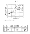
本発明者は、ワイヤ23のインダクタンスを1nHとし、第4層配線14Aの領域PADと領域31との間の距離L1(図1参照)を0μm、50μmおよび100μmの3通りに設定した場合における第4層配線14Aの信号反射特性の容量依存性について実験により調べた。図5に示すように、その距離L1が大きくなるに従って、第4層配線14Aを伝わる信号の周波数に対する電圧定在波比(Voltage Standing Wave Ratio;VSWR)は小さくなる。この電圧定在波比が小さくなるということは、上記第1層配線11(図1〜図3参照)、第4層配線14Aおよび層間絶縁膜15(図1〜図3参照)を用いて形成したキャパシタの容量値が大きくなり、伝送信号の損失が大きくなることになる。前述したように、本実施の形態1の半導体装置は光通信用ICであり、第4層配線14Aを伝わる信号の周波数は12GHz程度以下である。図5に示したように、上記距離L1が100μmである第4層配線14Aにこのような周波数帯の信号が伝わる場合には、伝送信号の損失が大きくなることから、距離L1を100μmで設計することは不適ということになる。一方、電圧定在波比が大きくなるということは、第4層配線14Aを伝わる信号の反射が大きくなるということになる。また前述したように、第4層配線14Aを伝わる信号の伝送速度(周波数)が大きくなるに従って伝送信号の反射は大きくなるものであり、本実施の形態1の半導体装置は光通信用ICであることから、第4層配線14Aには高周波(たとえば周波数1GHz程度以上)信号が伝わる。そのため、図5に示したように、距離L1が0μmである場合には、第4層配線14Aを伝わる信号の反射が大きくなり、距離L1を0μmで設計することは不適ということになる。そこで、距離L1を0μmと100μmとの間の50μmで設計すると、第4層配線14Aにおける伝送信号の損失および反射の双方を防ぐことが可能となる。なお、本発明者による実験においては、距離L1を50μmとすることで第4層配線14Aにおける伝送信号の損失および反射の双方を防ぐことが可能となったが、この距離L1は、第4層配線14A以外の部材の設計値に合わせて変更可能であることは言うまでもない。
【0024】
上記したように、本実施の形態1によれば、ワイヤ23を用いたワイヤボンディング法によって半導体チップ21とアウターリード22Bとを電気的に接続した場合において、パッケージ内の信号伝送線路の特性インピーダンス整合をとることができる。それにより、本実施の形態1の光通信用ICにおいては、信号の伝送速度を向上することができる。また、第4層配線14Aにおける伝送信号の損失および反射の双方を防ぐことができるので、伝送信号の波形が歪んでしまうことを防ぐことができる。それにより、本実施の形態1の半導体装置の信号の受信感度を向上することができる。
【0025】
(実施の形態2)
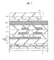
次に、本実施の形態2の半導体装置について説明する。図6は本実施の形態2の半導体装置の要部平面図であり、図7は図6中のA−A線に沿った断面図であり、図8は図6中のB−B線に沿った断面図である。
【0026】
本実施の形態2の半導体装置は、前記実施の形態1の半導体装置における第1層配線11(図1〜図3参照)の平面形状を変化させたものである。すなわち、図6〜図8に示すように、ボンディングパッドとなっている第4層配線14A、14Bの端部の領域PADの下部に、第1層配線11が配置されないように第1層配線11をパターニングするものである。これにより、領域PADにおいては、第4層配線14A、14Bと第1層配線11との間に第4層配線14A、14Bおよび第1層配線11より相対的に機械的強度の小さい層間絶縁膜15は存在しないことになるので、そのボンディングパッドにワイヤ23(図4参照)をボンディングする際の衝撃を緩和することができる。その結果、層間絶縁膜15にクラックが生じてしまうことを防ぐことができる。
【0027】
上記のような本実施の形態2の半導体装置によっても、前記実施の形態1の半導体装置と同様の効果を得ることができる。
【0028】
(実施の形態3)
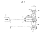
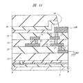
次に、本実施の形態3の半導体装置について説明する。図9は本実施の形態3の半導体装置の要部平面図であり、図10は図9中のA−A線に沿った断面図であり、図11は図9中のB−B線に沿った断面図である。
【0029】
本実施の形態3の半導体装置は、前記実施の形態3の半導体装置における第1層配線11(図1〜図3参照)の平面形状を変化させたものである。すなわち、平面において第1層配線11を領域PADに配置されるようにパターニングするものである。それにより、平面において前記実施の形態1の場合より小面積の第1層配線11と第4層配線14Aとを用いて容量成分を形成し、本実施の形態3のパッケージ内の信号伝送線路の特性インピーダンス整合をとることができる。
【0030】
上記のような本実施の形態3の半導体装置によっても、前記実施の形態1の半導体装置と同様の効果を得ることができる。
【0031】
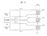
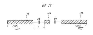
(実施の形態4)
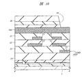
次に、本実施の形態4の半導体装置について説明する。図12は本実施の形態4の半導体装置の要部平面図であり、図13は図12中のC−C線に沿った断面図である。
【0032】
本実施の形態2の半導体装置は、前記実施の形態1の半導体装置における第4層配線(第3配線)14B(図1〜図3参照)の平面形状を変化させたものである。すなわち、図12および図13に示すように、本実施の形態4の半導体装置において第4層配線14A、14Bは、一定の間隔を隔てて配置されるコプレーナ構造を形成するものである。これにより、第4層配線14Aと第4層配線14Bとの間で、容量成分C1を形成することができる。このような容量成分C1を形成することによっても、パッケージ内の信号伝送線路の特性インピーダンス整合をとることができる。また、その容量成分C1は、第4層配線14A、14Bの厚さt、および第4層配線14Aと第4層配線14Bとの間隔sが要素となって決定されるものである。そのため、これらの値に比べて大きな3層の層間絶縁膜15(図2および図3参照)の膜厚の制御によって容量値を制御する前記実施の形態1に比べて、本実施の形態4における容量成分C1の容量値の制御を容易にすることができる。
【0033】
上記のような本実施の形態4の半導体装置によっても、前記実施の形態1の半導体装置と同様の効果を得ることができる。
【0034】
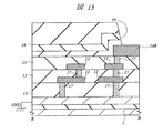
(実施の形態5)
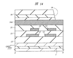
次に、本実施の形態5の半導体装置について説明する。図14および図15は、本実施の形態5の半導体装置の要部断面図である。
【0035】
本実施の形態5の半導体装置は、前記実施の形態1における第1層配線11(図1〜図3参照)を省略したものである。すなわち、図14および図15に示すように、半導体基板1のSOI層を接地(基準)電位(GND)と電気的に接続し、第4層配線14Bと電気的に接続する第2層配線12をプラグ17を介してそのSOI層と電気的に接続したものである。これにより、本実施の形態5においては、前記実施の形態1において第1層配線11と第4層配線14Aとの間で形成した容量成分と同様の容量成分を半導体基板(SOI層)と第4層配線14Aとの間で形成することができる。その結果、本実施の形態5によれば、第1層配線11を形成する工程を省略することができるので、本実施の形態5の半導体装置の製造工程数を低減することができる。すなわち、本実施の形態5の半導体装置の製造に要するTAT(Turn Around Time)を短縮することが可能となる。
【0036】
上記のような本実施の形態5の半導体装置によっても、前記実施の形態1の半導体装置と同様の効果を得ることができる。
【0037】
以上、本発明者によってなされた発明を発明の実施の形態に基づき具体的に説明したが、本発明は前記実施の形態に限定されるものではなく、その要旨を逸脱しない範囲で種々変更可能であることは言うまでもない。
【0038】
前記実施の形態においては、第1層配線と第4層配線との間に2層の配線が形成されている場合について例示したが、1層の配線または3層以上の配線としてもよい。
【0039】
【発明の効果】
本願によって開示される発明のうち、代表的なものによって得られる効果を簡単に説明すれば以下の通りである。
(1)接地電位と電気的に接続する第1配線およびボンディングワイヤが接続されるパッドとなる第2配線を容量電極とし、第1配線と第2配線との間の第1絶縁膜を容量絶縁膜とする容量成分を形成するので、高速LSIが形成された半導体チップを搭載するパッケージをワイヤボンディング法を用いて形成する場合においてもパッケージ内の信号伝送線路の特性インピーダンス整合をとることができる。
(2)高速LSIが形成された半導体チップが搭載されたパッケージにおいて、信号伝送線路の特性インピーダンス整合をとることができるので、信号伝送線路を伝わる信号が高周波であっても信号の反射を防ぐことができる。
【図面の簡単な説明】
【図1】本発明の実施の形態1である半導体装置の要部平面図である。
【図2】図1中のA−A線に沿った断面図である。
【図3】図1中のB−B線に沿った断面図である。
【図4】本発明の実施の形態1である半導体装置の要部断面図である。
【図5】本発明の実施の形態1である半導体装置における信号伝送線路の信号反射特性の容量依存性について示す説明図である。
【図6】本発明の実施の形態2である半導体装置の要部平面図である。
【図7】図6中のA−A線に沿った断面図である。
【図8】図6中のB−B線に沿った断面図である。
【図9】本発明の実施の形態3である半導体装置の要部平面図である。
【図10】図9中のA−A線に沿った断面図である。
【図11】図9中のB−B線に沿った断面図である。
【図12】本発明の実施の形態4である半導体装置の要部平面図である。
【図13】図12中のC−C線に沿った断面図である。
【図14】本発明の実施の形態5である半導体装置の要部断面図である。
【図15】本発明の実施の形態5である半導体装置の要部断面図である。
【符号の説明】
1 半導体基板
11 第1層配線(第1配線)
12 第2層配線
13 第3層配線
14A 第4層配線(第2配線)
14B 第4層配線(第3配線)
15 層間絶縁膜(第1絶縁膜)
17 プラグ
18 保護膜
19 開口部
21 半導体チップ
22A ダイパッド
22B アウターリード
23 ワイヤ
24 エポキシ樹脂
31 領域(第2領域)
32 領域
CAPA 領域(第1領域)
IO I/O回路(第1回路)
PAD 領域(パッド領域)[0001]
BACKGROUND OF THE INVENTION
The present invention relates to a semiconductor device, and more particularly to a technique effective when applied to a semiconductor device that requires high-frequency signal transmission and broadband high-speed signal transmission.
[0002]
[Prior art]
For example, a package mounting a semiconductor chip on which a high-speed LSI such as an optical communication IC is mounted is required to transmit a signal in a wide band from DC to a high frequency band actually used. In particular, at a bit rate of 10 Gbit / sec or higher, the package is required to have impedance matching and low loss at a high frequency. As a countermeasure against such a requirement, a semiconductor chip is mounted in a face-down manner on the main surface of the package substrate on which the signal transmission line is formed, and one end of the signal transmission line is directly below the electrode pad formed on the main surface of the semiconductor chip. By extending, a means for mounting the signal transmission line and the electrode pad so as to be electrically connected via the bump electrode is conceivable. According to this means, the signal transmission line and the semiconductor chip can be connected with the shortest distance, so that the transmission characteristics from the signal transmission line to the electrode pad of the semiconductor chip can be well preserved. By using ceramic as the packaging material, a transmission line with low loss and impedance matching can be formed. Further, by sealing hermetically using ceramic as a packaging material, the semiconductor chip can be protected from the external environment, and a package having excellent mechanical strength, moisture resistance, heat resistance, heat dissipation, and the like can be realized.
[0003]
For example, in Japanese Patent Application Laid-Open No. 7-147352, the wiring width of a signal transmission line formed on a package substrate is narrowed in a region overlapping with a semiconductor chip, resulting from a capacitance formed between the semiconductor chip and the signal transmission line. A technique for matching characteristic impedance of a signal transmission line in a package by compensating for a decrease in impedance is disclosed. Also disclosed is a technique for reducing transmission signal loss in a package by using a package substrate made of ceramic.
[0004]
[Problems to be solved by the invention]
When the semiconductor chip is mounted on the main surface of the package substrate as described above by the face-down method, it is necessary to form bump electrodes (solder balls) on the electrode pads formed on the main surface of the semiconductor chip. The bump electrode is formed on the electrode pad using a plating method or the like after forming and patterning a photoresist film on the main surface of the semiconductor wafer before cutting into individual semiconductor chips. Therefore, for example, the number of processing steps for the semiconductor wafer is increased as compared with the means for mounting by wire bonding the electrode pad and the package substrate, and the manufacturing cost of the semiconductor wafer is increased. It will be.
[0005]
Further, since the semiconductor chip is mounted by the face-down method, the connection portion between the bump electrode and the package substrate cannot be visually recognized during the mounting process. For this reason, for example, since it becomes difficult to mount the semiconductor chip on the package substrate by wire bonding, the manufacturing cost of the package becomes expensive.
[0006]
In addition, when ceramic is used as the packaging material, the material cost becomes higher than when plastic is used, for example, and the manufacturing cost of the package becomes high.
[0007]
Therefore, the present inventor is examining means for forming a package on which a semiconductor chip on which a high-speed LSI is formed is formed using a wire bonding method and a packaging method using plastic such as epoxy resin as a packaging material. Among them, the present inventors have found the following problems.
[0008]
In other words, the use of the wire bonding method increases the impedance in the bonding wire portion, so that the transmission characteristics from the signal transmission line to the electrode pad of the semiconductor chip cannot be well preserved. Exists.
[0009]
An object of the present invention is to provide means for forming a package for mounting a semiconductor chip on which a high-speed LSI is formed, using a wire bonding method.
[0010]
The above and other objects and novel features of the present invention will be apparent from the description of this specification and the accompanying drawings.
[0011]
[Means for Solving the Problems]
Of the inventions disclosed in the present application, the outline of typical ones will be briefly described as follows.
[0012]
That is, the present invention provides a first wiring formed on a semiconductor substrate and electrically connected to a ground potential, a first insulating film formed on the first wiring, and formed on the first insulating film. And a second wiring that is a signal transmission line, the second wiring including a first region, a second region, and a third region, and a bonding wire connected to the first region of the second wiring. The wiring width in the second region of the second wiring is larger than the wiring width in the third region.
[0013]
DETAILED DESCRIPTION OF THE INVENTION
Hereinafter, embodiments of the present invention will be described in detail with reference to the drawings. Note that components having the same function are denoted by the same reference symbols throughout the drawings for describing the embodiments, and the repetitive description thereof will be omitted. Further, in the drawings used for the description of the following embodiments, hatching may be given even in plan views for easy understanding of the drawings.
[0014]
(Embodiment 1)
The semiconductor device of the first embodiment is a package on which a semiconductor chip on which an optical communication IC (high speed LSI) is formed is mounted, for example. 1 is a plan view of a principal part of the semiconductor device according to the first embodiment, FIG. 2 is a cross-sectional view taken along line AA in FIG. 1, and FIG. 3 is taken along line BB in FIG. FIG. 4 is a cross-sectional view of a main part of the semiconductor device according to the first embodiment.
[0015]
As shown in FIGS. 2 and 3, the semiconductor device of the first embodiment includes, for example, a single crystal silicon (SOI (Silicon On Insulator) layer) serving as a bond substrate on which a semiconductor element is formed and a single crystal serving as a base substrate. The
[0016]
On the
[0017]
The fourth layer wiring (second wiring) 14 </ b> A is a signal transmission line and is electrically connected to the I /
[0018]
As shown in FIG. 4, the
[0019]
By the way, the line impedance Z in the package of the first embodiment can be simply expressed as Z = (L / C) 1/2 where L is the inductance and C is the capacitance. The line impedance Z is defined by a predetermined value (first value) such as 50Ω in order to match the characteristic impedance of the signal transmission line in the package. As described above, in the first embodiment, means for wire bonding the
[0020]
Further, when a capacitor having a predetermined capacitance value is formed using the
[0021]
Further, the fourth-
[0022]
Further, as described above, the region PAD of the
[0023]
The inventor sets the inductance of the
[0024]
As described above, according to the first embodiment, when the
[0025]
(Embodiment 2)
Next, the semiconductor device of the second embodiment will be described. 6 is a plan view of a principal part of the semiconductor device according to the second embodiment, FIG. 7 is a cross-sectional view taken along line AA in FIG. 6, and FIG. 8 is taken along line BB in FIG. FIG.
[0026]
The semiconductor device according to the second embodiment is obtained by changing the planar shape of the first layer wiring 11 (see FIGS. 1 to 3) in the semiconductor device according to the first embodiment. That is, as shown in FIGS. 6 to 8, the
[0027]
Also by the semiconductor device of the second embodiment as described above, the same effect as that of the semiconductor device of the first embodiment can be obtained.
[0028]
(Embodiment 3)
Next, the semiconductor device according to the third embodiment will be described. 9 is a plan view of a principal part of the semiconductor device according to the third embodiment, FIG. 10 is a cross-sectional view taken along line AA in FIG. 9, and FIG. 11 is taken along line BB in FIG. FIG.
[0029]
The semiconductor device of the third embodiment is obtained by changing the planar shape of the first layer wiring 11 (see FIGS. 1 to 3) in the semiconductor device of the third embodiment. That is, the first-
[0030]
Also by the semiconductor device of the third embodiment as described above, the same effect as that of the semiconductor device of the first embodiment can be obtained.
[0031]
(Embodiment 4)
Next, the semiconductor device according to the fourth embodiment will be described. 12 is a plan view of an essential part of the semiconductor device according to the fourth embodiment, and FIG. 13 is a cross-sectional view taken along the line CC in FIG.
[0032]
The semiconductor device of the second embodiment is obtained by changing the planar shape of the fourth layer wiring (third wiring) 14B (see FIGS. 1 to 3) in the semiconductor device of the first embodiment. That is, as shown in FIGS. 12 and 13, in the semiconductor device of the fourth embodiment, the
[0033]
Also by the semiconductor device of the fourth embodiment as described above, the same effect as that of the semiconductor device of the first embodiment can be obtained.
[0034]
(Embodiment 5)
Next, the semiconductor device of the fifth embodiment will be described. 14 and 15 are cross-sectional views of main parts of the semiconductor device according to the fifth embodiment.
[0035]
In the semiconductor device of the fifth embodiment, the first layer wiring 11 (see FIGS. 1 to 3) in the first embodiment is omitted. That is, as shown in FIGS. 14 and 15, the
[0036]
Also by the semiconductor device of the fifth embodiment as described above, the same effect as that of the semiconductor device of the first embodiment can be obtained.
[0037]
As mentioned above, the invention made by the present inventor has been specifically described based on the embodiments of the invention. However, the present invention is not limited to the above-described embodiments, and various modifications can be made without departing from the scope of the invention. Needless to say.
[0038]
In the above embodiment, the case where two layers of wiring are formed between the first layer wiring and the fourth layer wiring is illustrated, but one layer wiring or three or more layers wiring may be used.
[0039]
【The invention's effect】
Among the inventions disclosed by the present application, effects obtained by typical ones will be briefly described as follows.
(1) The first wiring electrically connected to the ground potential and the second wiring serving as a pad to which the bonding wire is connected are used as capacitive electrodes, and the first insulating film between the first wiring and the second wiring is capacitively insulated. Since the capacitive component that forms the film is formed, the characteristic impedance matching of the signal transmission line in the package can be achieved even when the package on which the semiconductor chip on which the high-speed LSI is formed is formed using the wire bonding method.
(2) In a package on which a semiconductor chip on which a high-speed LSI is formed is mounted, it is possible to match the characteristic impedance of the signal transmission line, thereby preventing signal reflection even if the signal transmitted through the signal transmission line is high frequency. Can do.
[Brief description of the drawings]
FIG. 1 is a plan view of an essential part of a semiconductor device according to a first embodiment of the present invention.
FIG. 2 is a cross-sectional view taken along line AA in FIG.
FIG. 3 is a cross-sectional view taken along line BB in FIG.
4 is a fragmentary cross-sectional view of the semiconductor device according to the first embodiment of the present invention; FIG.
FIG. 5 is an explanatory diagram showing capacitance dependency of signal reflection characteristics of a signal transmission line in the semiconductor device according to the first embodiment of the present invention;
6 is a plan view of relevant parts of a semiconductor device according to a second embodiment of the present invention; FIG.
7 is a cross-sectional view taken along the line AA in FIG.
8 is a cross-sectional view taken along line BB in FIG.
FIG. 9 is a fragmentary plan view of a semiconductor device according to a third embodiment of the present invention;
10 is a cross-sectional view taken along line AA in FIG.
11 is a cross-sectional view taken along line BB in FIG.
12 is a plan view of relevant parts of a semiconductor device according to a fourth embodiment of the present invention; FIG.
13 is a cross-sectional view taken along the line CC in FIG.
FIG. 14 is a fragmentary cross-sectional view of a semiconductor device according to a fifth embodiment of the present invention;
FIG. 15 is a fragmentary cross-sectional view of a semiconductor device according to a fifth embodiment of the present invention;
[Explanation of symbols]
12 Second-
14B Fourth layer wiring (third wiring)
15 Interlayer insulation film (first insulation film)
17
32 area CAPA area (first area)
IO I / O circuit (first circuit)
PAD area (pad area)
Claims (16)
前記第1配線上に形成された第1絶縁膜と、
前記第1絶縁膜上に形成され、信号伝送線路である第2配線と
を有し、
前記第2配線は第1領域と第2領域と第3領域とを含み、
前記第2配線の前記第2領域は、前記第1領域および前記第3領域の間に位置し、
前記第2配線の前記第1領域にはボンディングワイヤが接続され、
前記第2配線の前記第2領域における配線幅は前記第3領域における配線幅よりも大きく、
前記第1配線と前記第2配線とは、互いに該第1配線および該第2配線を容量電極とするキャパシタを構成し、
前記キャパシタは、前記ボンディングワイヤの有するインダクタンス成分に対して、前記信号伝送線路の特性インピーダンス整合を取るように作用することを特徴とする半導体装置。A first wiring formed on the semiconductor substrate and electrically connected to a ground potential;
A first insulating film formed on the first wiring;
A second wiring that is formed on the first insulating film and is a signal transmission line;
The second wiring includes a first region, a second region, and a third region,
The second region of the second wiring is located between the first region and the third region;
A bonding wire is connected to the first region of the second wiring,
Wiring width in the second region of the second wiring much larger than the wiring width of the third region,
The first wiring and the second wiring constitute a capacitor having the first wiring and the second wiring as capacitance electrodes,
The semiconductor device is characterized in that the capacitor acts to achieve characteristic impedance matching of the signal transmission line with respect to an inductance component of the bonding wire .
前記第2配線の前記第1領域は、下部に前記第1配線の存在しない位置に配置されていることを特徴とする半導体装置。The semiconductor device according to claim 1,
The semiconductor device according to claim 1, wherein the first region of the second wiring is arranged at a position where the first wiring does not exist in a lower portion.
前記第1配線は前記第2配線の前記第1領域の下部に配置されていることを特徴とする半導体装置。The semiconductor device according to claim 1,
The semiconductor device, wherein the first wiring is disposed below the first region of the second wiring.
前記第2配線を含む第2配線層は接地電位と電気的に接続された第3配線を含み、前記第2配線と前記第3配線とは一定の間隔を隔てて配置され、前記第2配線および前記第3配線を容量電極とする容量成分が形成されていることを特徴とする半導体装置。The semiconductor device according to claim 1,
The second wiring layer including the second wiring includes a third wiring electrically connected to a ground potential, and the second wiring and the third wiring are arranged at a predetermined interval, and the second wiring And a capacitance component having the third wiring as a capacitance electrode is formed.
前記第1配線を含む第1配線層と前記第2配線を含む第2配線層との間には、少なくとも1層の配線層が形成されていることを特徴とする半導体装置。The semiconductor device according to claim 1,
A semiconductor device, wherein at least one wiring layer is formed between a first wiring layer including the first wiring and a second wiring layer including the second wiring.
前記第2配線の前記第2領域は平面順テーパー形状で形成されていることを特徴とする半導体装置。The semiconductor device according to claim 1,
2. The semiconductor device according to claim 1, wherein the second region of the second wiring is formed in a planar forward tapered shape.
前記第2配線における前記第1領域は、前記第2配線の端部に配置されていることを特徴とする半導体装置。The semiconductor device according to claim 1,
The semiconductor device according to claim 1, wherein the first region of the second wiring is disposed at an end portion of the second wiring.
前記第2配線の前記第3領域は、前記半導体基板上に形成された第1回路に向かって延在し、前記第1回路と電気的に接続していることを特徴とする半導体装置。The semiconductor device according to claim 1,
The semiconductor device, wherein the third region of the second wiring extends toward the first circuit formed on the semiconductor substrate and is electrically connected to the first circuit.
前記第1配線および前記第2配線の前記第3領域は、マイクロストリップ構造を形成していることを特徴とする半導体装置。The semiconductor device according to claim 1,
The semiconductor device according to claim 1, wherein the third region of the first wiring and the second wiring forms a microstrip structure.
前記第2配線の線路インピーダンスは、所定の第1の値であることを特徴とする半導体装置。The semiconductor device according to claim 1,
The semiconductor device according to claim 1, wherein the line impedance of the second wiring is a predetermined first value.
前記半導体基板上に形成され、信号伝送線路である第2配線と
を有し、
前記第2配線は第1領域と第2領域と第3領域とを含み、
前記第2配線の前記第2領域は、前記第1領域および前記第3領域の間に位置し、
前記第2配線の前記第1領域にはボンディングワイヤが接続され、
前記第2配線の前記第2領域における配線幅は前記第3領域における配線幅よりも大きく、
前記半導体基板と前記第2配線とは、互いに該半導体基板および該第2配線を容量電極とするキャパシタを構成し、
前記キャパシタは、前記ボンディングワイヤの有するインダクタンス成分に対して、前記信号伝送線路の特性インピーダンス整合を取るように作用することを特徴とする半導体装置。A semiconductor substrate electrically connected to a ground potential;
A second wiring formed on the semiconductor substrate and serving as a signal transmission line;
The second wiring includes a first region, a second region, and a third region,
The second region of the second wiring is located between the first region and the third region;
A bonding wire is connected to the first region of the second wiring,
Wiring width in the second region of the second wiring much larger than the wiring width of the third region,
The semiconductor substrate and the second wiring constitute a capacitor having the semiconductor substrate and the second wiring as capacitance electrodes,
The semiconductor device is characterized in that the capacitor acts to achieve characteristic impedance matching of the signal transmission line with respect to an inductance component of the bonding wire .
前記半導体基板と前記第2配線を含む第2配線層との間には、少なくとも1層の配線層が形成されていることを特徴とする半導体装置。The semiconductor device according to claim 11.
A semiconductor device, wherein at least one wiring layer is formed between the semiconductor substrate and a second wiring layer including the second wiring.
前記第2配線の前記第2領域は平面順テーパー形状で形成されていることを特徴とする半導体装置。The semiconductor device according to claim 11.
2. The semiconductor device according to claim 1, wherein the second region of the second wiring is formed in a planar forward tapered shape.
前記第2配線の前記第3領域は、前記半導体基板上に形成された第1回路に向かって延在し、前記第1回路と電気的に接続していることを特徴とする半導体装置。The semiconductor device according to claim 11.
The semiconductor device, wherein the third region of the second wiring extends toward the first circuit formed on the semiconductor substrate and is electrically connected to the first circuit.
前記半導体基板および前記第2配線の前記第3領域は、マイクロストリップ構造を形成していることを特徴とする半導体装置。The semiconductor device according to claim 11.
The semiconductor device, wherein the third region of the semiconductor substrate and the second wiring forms a microstrip structure.
前記第2配線の線路インピーダンスは、所定の第1の値であることを特徴とする半導体装置。The semiconductor device according to claim 11.
The semiconductor device according to claim 1, wherein the line impedance of the second wiring is a predetermined first value.
Priority Applications (1)
| Application Number | Priority Date | Filing Date | Title |
|---|---|---|---|
| JP2002165554A JP4231663B2 (en) | 2002-06-06 | 2002-06-06 | Semiconductor device |
Applications Claiming Priority (1)
| Application Number | Priority Date | Filing Date | Title |
|---|---|---|---|
| JP2002165554A JP4231663B2 (en) | 2002-06-06 | 2002-06-06 | Semiconductor device |
Publications (2)
| Publication Number | Publication Date |
|---|---|
| JP2004014771A JP2004014771A (en) | 2004-01-15 |
| JP4231663B2 true JP4231663B2 (en) | 2009-03-04 |
Family
ID=30433364
Family Applications (1)
| Application Number | Title | Priority Date | Filing Date |
|---|---|---|---|
| JP2002165554A Expired - Fee Related JP4231663B2 (en) | 2002-06-06 | 2002-06-06 | Semiconductor device |
Country Status (1)
| Country | Link |
|---|---|
| JP (1) | JP4231663B2 (en) |
Families Citing this family (3)
| Publication number | Priority date | Publication date | Assignee | Title |
|---|---|---|---|---|
| JP2005302773A (en) * | 2004-04-06 | 2005-10-27 | Nippon Telegr & Teleph Corp <Ntt> | Tournament distribution and synthesis circuit |
| JP6149503B2 (en) * | 2013-05-17 | 2017-06-21 | 住友電気工業株式会社 | Semiconductor device |
| JP2021086916A (en) * | 2019-11-27 | 2021-06-03 | ソニーセミコンダクタソリューションズ株式会社 | Driver circuit |
-
2002
- 2002-06-06 JP JP2002165554A patent/JP4231663B2/en not_active Expired - Fee Related
Also Published As
| Publication number | Publication date |
|---|---|
| JP2004014771A (en) | 2004-01-15 |
Similar Documents
| Publication | Publication Date | Title |
|---|---|---|
| US6924549B2 (en) | Semiconductor device and a method of manufacturing the same | |
| US5317107A (en) | Shielded stripline configuration semiconductor device and method for making the same | |
| JP2601867B2 (en) | Semiconductor integrated circuit mounting substrate, method of manufacturing the same, and semiconductor integrated circuit device | |
| US5976911A (en) | Controlling impedances of an integrated circuit | |
| EP3732708A1 (en) | Wire bonding between isolation capacitors for multichip modules | |
| JP2507476B2 (en) | Semiconductor integrated circuit device | |
| JP2978533B2 (en) | Semiconductor integrated circuit device | |
| JP2004079579A (en) | Semiconductor device | |
| JP7601773B2 (en) | Electronic device flip chip package with exposed clips - Patents.com | |
| JPH08222657A (en) | Semiconductor integrated circuit device | |
| TWI771888B (en) | semiconductor device | |
| JP3357435B2 (en) | Semiconductor integrated circuit device | |
| US5426319A (en) | High-frequency semiconductor device including microstrip transmission line | |
| WO2020170650A1 (en) | Semiconductor module, power semiconductor module, and power electronic equipment using either of same | |
| JPH03195049A (en) | Semiconductor integrated circuit device | |
| US20080197503A1 (en) | Chip package | |
| JP2012039020A (en) | High-frequency switch | |
| CN105895614A (en) | Semiconductor device and method of manufacturing the same | |
| JP2003163310A (en) | High frequency semiconductor device | |
| JP4231663B2 (en) | Semiconductor device | |
| JP2004134450A (en) | Semiconductor integrated circuit | |
| US9905517B2 (en) | Semiconductor device | |
| US7091594B1 (en) | Leadframe type semiconductor package having reduced inductance and its manufacturing method | |
| TWI740569B (en) | Wiring board and semiconductor device | |
| JP2006332708A (en) | Semiconductor device |
Legal Events
| Date | Code | Title | Description |
|---|---|---|---|
| A621 | Written request for application examination |
Free format text: JAPANESE INTERMEDIATE CODE: A621 Effective date: 20050311 |
|
| A977 | Report on retrieval |
Free format text: JAPANESE INTERMEDIATE CODE: A971007 Effective date: 20080331 |
|
| A131 | Notification of reasons for refusal |
Free format text: JAPANESE INTERMEDIATE CODE: A131 Effective date: 20080812 |
|
| A521 | Request for written amendment filed |
Free format text: JAPANESE INTERMEDIATE CODE: A523 Effective date: 20081009 |
|
| TRDD | Decision of grant or rejection written | ||
| A01 | Written decision to grant a patent or to grant a registration (utility model) |
Free format text: JAPANESE INTERMEDIATE CODE: A01 Effective date: 20081111 |
|
| A01 | Written decision to grant a patent or to grant a registration (utility model) |
Free format text: JAPANESE INTERMEDIATE CODE: A01 |
|
| A61 | First payment of annual fees (during grant procedure) |
Free format text: JAPANESE INTERMEDIATE CODE: A61 Effective date: 20081208 |
|
| R150 | Certificate of patent or registration of utility model |
Free format text: JAPANESE INTERMEDIATE CODE: R150 |
|
| FPAY | Renewal fee payment (event date is renewal date of database) |
Free format text: PAYMENT UNTIL: 20111212 Year of fee payment: 3 |
|
| FPAY | Renewal fee payment (event date is renewal date of database) |
Free format text: PAYMENT UNTIL: 20111212 Year of fee payment: 3 |
|
| FPAY | Renewal fee payment (event date is renewal date of database) |
Free format text: PAYMENT UNTIL: 20121212 Year of fee payment: 4 |
|
| FPAY | Renewal fee payment (event date is renewal date of database) |
Free format text: PAYMENT UNTIL: 20131212 Year of fee payment: 5 |
|
| LAPS | Cancellation because of no payment of annual fees |