JP4230195B2 - Multi-resolution photodiode sensor array for optical encoders - Google Patents
Multi-resolution photodiode sensor array for optical encoders Download PDFInfo
- Publication number
- JP4230195B2 JP4230195B2 JP2002315285A JP2002315285A JP4230195B2 JP 4230195 B2 JP4230195 B2 JP 4230195B2 JP 2002315285 A JP2002315285 A JP 2002315285A JP 2002315285 A JP2002315285 A JP 2002315285A JP 4230195 B2 JP4230195 B2 JP 4230195B2
- Authority
- JP
- Japan
- Prior art keywords
- photodiodes
- resolution
- groups
- output signal
- phase
- Prior art date
- Legal status (The legal status is an assumption and is not a legal conclusion. Google has not performed a legal analysis and makes no representation as to the accuracy of the status listed.)
- Expired - Fee Related
Links
- 230000003287 optical effect Effects 0.000 title claims abstract description 57
- 238000001514 detection method Methods 0.000 claims abstract description 19
- 238000005259 measurement Methods 0.000 claims description 6
- 238000000034 method Methods 0.000 abstract description 11
- 238000003491 array Methods 0.000 description 20
- 239000004065 semiconductor Substances 0.000 description 20
- 239000004020 conductor Substances 0.000 description 9
- 230000008859 change Effects 0.000 description 7
- 238000012545 processing Methods 0.000 description 5
- 238000012360 testing method Methods 0.000 description 5
- 230000004913 activation Effects 0.000 description 4
- 230000008901 benefit Effects 0.000 description 4
- 238000006243 chemical reaction Methods 0.000 description 4
- 238000004891 communication Methods 0.000 description 4
- 230000033001 locomotion Effects 0.000 description 4
- 230000008569 process Effects 0.000 description 4
- 230000006978 adaptation Effects 0.000 description 3
- 230000005540 biological transmission Effects 0.000 description 3
- 229910052573 porcelain Inorganic materials 0.000 description 3
- 238000013461 design Methods 0.000 description 2
- 238000011156 evaluation Methods 0.000 description 2
- 239000000758 substrate Substances 0.000 description 2
- 241000669069 Chrysomphalus aonidum Species 0.000 description 1
- 230000003213 activating effect Effects 0.000 description 1
- 230000003044 adaptive effect Effects 0.000 description 1
- 238000013459 approach Methods 0.000 description 1
- 230000000295 complement effect Effects 0.000 description 1
- 238000004590 computer program Methods 0.000 description 1
- 238000000354 decomposition reaction Methods 0.000 description 1
- 230000008030 elimination Effects 0.000 description 1
- 238000003379 elimination reaction Methods 0.000 description 1
- 238000005516 engineering process Methods 0.000 description 1
- 238000004519 manufacturing process Methods 0.000 description 1
- 230000007246 mechanism Effects 0.000 description 1
- 239000002184 metal Substances 0.000 description 1
- 238000000465 moulding Methods 0.000 description 1
- 239000012811 non-conductive material Substances 0.000 description 1
- 238000012805 post-processing Methods 0.000 description 1
- 238000002310 reflectometry Methods 0.000 description 1
- 230000004044 response Effects 0.000 description 1
- 230000000630 rising effect Effects 0.000 description 1
Images


Classifications
-
- G—PHYSICS
- G01—MEASURING; TESTING
- G01D—MEASURING NOT SPECIALLY ADAPTED FOR A SPECIFIC VARIABLE; ARRANGEMENTS FOR MEASURING TWO OR MORE VARIABLES NOT COVERED IN A SINGLE OTHER SUBCLASS; TARIFF METERING APPARATUS; MEASURING OR TESTING NOT OTHERWISE PROVIDED FOR
- G01D5/00—Mechanical means for transferring the output of a sensing member; Means for converting the output of a sensing member to another variable where the form or nature of the sensing member does not constrain the means for converting; Transducers not specially adapted for a specific variable
- G01D5/26—Mechanical means for transferring the output of a sensing member; Means for converting the output of a sensing member to another variable where the form or nature of the sensing member does not constrain the means for converting; Transducers not specially adapted for a specific variable characterised by optical transfer means, i.e. using infrared, visible, or ultraviolet light
- G01D5/32—Mechanical means for transferring the output of a sensing member; Means for converting the output of a sensing member to another variable where the form or nature of the sensing member does not constrain the means for converting; Transducers not specially adapted for a specific variable characterised by optical transfer means, i.e. using infrared, visible, or ultraviolet light with attenuation or whole or partial obturation of beams of light
- G01D5/34—Mechanical means for transferring the output of a sensing member; Means for converting the output of a sensing member to another variable where the form or nature of the sensing member does not constrain the means for converting; Transducers not specially adapted for a specific variable characterised by optical transfer means, i.e. using infrared, visible, or ultraviolet light with attenuation or whole or partial obturation of beams of light the beams of light being detected by photocells
- G01D5/36—Forming the light into pulses
Abstract
Description
【0001】
【発明の属する技術分野】
本発明は、様々な光学的な分解能に対して使用されるフォトダイオード・センサに関する。特に、本発明は、様々な分解能に対して使用される光学エンコーダ用のフォトセンサアレイに関する。
【0002】
【従来の技術】
2つの可動物体間の相対位置を測定する光学エンコーダが周知である。回転運動方向に沿って相対位置を測定することが可能であるのと同様に、直線運動方向に沿って相対位置を測定することが可能である。このシステムでは、一方の物体が多くの場合に走査目盛に連結されている一方で、他方の物体は走査ユニットに連結されている。リニアエンコーダの場合には直線目盛付きのリニアスケールが使用される一方で、ロータリーエンコーダの場合には円目盛付きのコードディスクが使用される。直線運動又は回転運動に対して使用される走査ユニットは、1つ以上の光源及び1つ以上の光電式検出素子を有する。例えば、フォトダイオードが、検出素子として多くの場合に使用される。
【0003】
近年、検出素子としての多数のフォトダイオードを互いに組合わせたリニアエンコーダとロータリーエンコーダが益々一般になってきている。このような検出配置は、時には位相アレイ(phased array)とも呼ばれる。このようなエンコーダと検出器は、米国特許発明第6,175,109 号明細書中に記されている。この全体の内容は、本明細書中では引用例によって記されている。
【0004】
上述した検出器の配置の実施の形態では、複数のフォトダイオードが半導体チップ上でアレイ状に配置されている。これらのフォトダイオードの配置は、固有の方法でエンコーダの構成ごとに注文/設計されなければならない。このことは、フォトダイオードの幅や間隔のようなフォトダイオードに要求される幾何学的な配置が、走査配置、特に走査される走査目盛の目盛周期に依存することを意味する。或る特定の測定分解能に対して、フォトダイオードの良好に規定された配置が存在する。したがって、走査配置又はエンコーダの分解能を変更する必要がある場合は、フォトダイオードの配置を変更して、所望の走査配置又は分解能にする必要がある。この場合、多大な設計作業が、このフォトダイオードアレイのレイアウトを変更するために必要である。
【0005】
この問題を解決するため、ヨーロッパ特許発明第0 710 819 号明細書は、異なる目盛周期を呈する幾つかの異なる走査目盛用の複数のフォトダイオードを有する単一のフォトダイオード・アセンブリーを使用することを提唱する。この目的のために、入手可能なフォトダイオードのうちの或る特定の数のフォトダイオードだけが、走査目盛に応じて起動されなければならない。フォトダイオードのうちのどのフォトダイオードが、或る特定の走査目盛に対して起動されなければならないのかをその都度決定するために、適合処理が必要である。複雑なASICをこの適合処理を制御するために要する点が、このシステムの主要な欠点である。システムの起動位相(adaptation phase)が特別なツーリング・ ディスク(tooling discs) を必要とする点がもう1つの欠点である。さらに、大きなメモリ空間と関連する回路が、キャリア基板上に必要である。このキャリア基板は、システムの可能な小型化に反する。
【0006】
ヨーロッパ特許発明第0 710 819 号明細書中に記載のシステムのもう1つの欠点は、絶対位置を測定するシステムのインデックス・ センサである。特に、インデックス・ センサのパターンに一致する開口部のパターンを有するディスクが、光をこれらのインデックス・ センサに通過させることを可能にする。この光は、1回転当り一点だけでインデックス・ センサを照射する。インデックス・ センサの一部が照射されているときの信号は、インデックス・ センサの全体が同時に照射されているときよりも著しく小さい。
【0007】
【発明が解決しようとする課題】
本発明の課題は、検出器アレイを所望の小型の大きさにすることが可能である一方で、この検出器アレイの分解能を容易に変更することにある。
【0008】
本発明のもう1つの課題は、適合位相を使用することなしに検出器アレイの分解能を変更することにある。
【0009】
本発明のもう1つの課題は、多重分解能において検出器アレイによって生成される絶対位置信号と相対位置信号の強度を向上させることにある。
【0010】
本発明の第1の側面は、或る特定の測定方向に沿って移動する物体の位置情報を提供する光学エンコーダに関する。このエンコーダは、光を放出する光源、及びこの光源に対して相対運動する物体に付されたデータトラックを有する。このデータトラックは、光を受け、かつ特定の分解能の異なる光学特性を呈する複数の可変領域を有する。検出システムが、データトラックから変調された光を受けて、その受けた光から位置信号を生成する。この検出システムは、データトラックから変調された光を受けるフォトダイオードアレイ、及びこのフォトダイオードアレイに接続された分解能選択ユニットを有する。この分解能選択ユニットは、フォトダイオードアレイの分解能を制御する。この場合、フォトダイオードアレイに関連する全てのフォトダイオードが、分解能選択ユニットによって選択された分解能に関係なく起動している。
【0011】
本発明の第2の側面は、或る特定の測定方向に沿って移動する物体の位置情報を提供する光学エンコーダの分解能を制御する方法に関する。この場合、光学エンコーダは、光を放射する光源、及びこの光源に対して相対運動するデータトラックを有する。
【0012】
本発明の第3の側面は、物体の位置情報を提供する光学エンコーダに関する。この光学エンコーダは、光を放出する光源、及びこの光源に対して相対運動する物体に装着されたデータトラックを有する。データトラックは、光を受信し、かつ特定の分解能の異なる光学特性の交互になっている領域を有する。検出装置が、データトラックから光を受信して、この受信した光からインデックス信号を生成する。検出システムは、データトラックから光を受信してインデックス信号を生成するインデックス・フォトダイオードアレイ、及びこのインデックス・フォトダイオードアレイに接続された分解能選択ユニットを有する。この分解能選択ユニットは、インデックス信号を制御する。
【0013】
本発明の第4の側面は、所定の測定方向に沿って運動する物体の位置情報を提供する光学エンコーダのインデックス信号を制御する方法に関する。この場合、光学エンコーダは、光を放射する光源、及びこの光源に対して相対運動しかつ与えられた分解能を呈するデータトラックを有する。この方法は、インデックス・フォトダイオードアレイのフォトダイオードの配置を変更することなしに、データトラックからインデックス・フォトダイオードアレイの複数のフォトダイオードへの光を検出し、インデックス・フォトダイオードアレイの1つ以上のフォトダイオードの活性状態を変えて、インデックス信号を生成する。
【0014】
本発明の各側面は、検出器アレイの分解能を容易に変更する一方で、検出器アレイを適切に小型の大きさにすることが可能である。
【0015】
本発明の各側面は、特定の分解能に対するアレイ内で活性化すべきフォトダイオードを決定するための適合位相を要求しない利点を提供する。起動位相が不要であることは、ヨーロッパ特許発明第0 710 819 号明細書中に記されたシステムに対して必要であるような特別なツーリング・ディスクが要求されないという利点をさらに提供する。
【0016】
【発明の実施の形態】
以下に、これらの事項及び本発明のその他の特徴と利点を図面に基づいて詳しく説明する。
【0017】
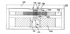
図1は、本発明の好適な実施例の光学エンコーダの断面を概略的に示す。特に、示された光学エンコーダは、回転している2つの物体の運動に関する位置情報を生成するロータリーエンコーダ100である。ロータリーエンコーダ100は、例えばブラシレス・モータを伴う用途で使用され得る。
【0018】
光学エンコーダ100は、図1−3,5,6,8,9,11中に示されたようにシングルデータトラック104を有するコード歯車102を含む。このコード歯車102は、軸線の周りで回転するシャフト(図示せず)上に設置されていて、かつ測定方向に沿って運動/回転する。回転シャフトは、ブラシレスDCモータの回転子でもよい。さらに、光学エンコーダ100は、データトラック104を光電式に走査する走査ユニット106を有する。図1中に示したように、走査ユニット106は、光源110及びレンズ112、好ましくは集光レンズ又は集束レンズを有する。機構的な構造の細部は当業者にとって周知であるので、エンコーダ100の構造は、概略的にしか示されていない。
【0019】
図1,2中に示したように、光源110によって放出された光114は、集光レンズ112によって平行にされ、光源110に対して回転するコード歯車102のデータトラック104を通じて伝送される。回転しているデータトラック104によって変調された光116は、検出システム120の光検出器アレイ118によって受信される。検出された信号が、図1,2中に示されていない評価ユニット内で処理される。
【0020】
図1−3,5,6,8,9,11中に示したように、データトラック104は、交互になっている透明なバー122と不透明なバー124のような、異なる光学特性の交互になっている領域の増分式のパターンを有する。光学エンコーダ100が入射光データトラックを使用するために構成されている場合には、このデータトラックを高反射度と低反射度が交互になっている領域で構成することが可能である。さらに、光検出器アレイ118は、1つの増分式フォトダイオードアレイ126と2つのインデックス・フォトダイオードアレイ128,130から構成される。フォトダイオードアレイ126,128,130はそれぞれ、複数のフォトダイオード132,134,136を有する。これらのフォトダイオード132,134,136は、オプト・ASIC半導体チップ138上に分離したアレイで配置されている。このオプト・ASIC半導体チップ138は、PCボード139上に搭載されている。
【0021】
図3−11中に示したように、増分式フォトダイオードアレイ126は、96個のフォトダイオード132を有する。この場合、隣合ったフォトダイオードは、互いに等角に配置されている。そして、グループとしてのこれらのフォトダイオードが、約9.2 °の角度、例えば9.22°の角度の範囲を定める。その結果、個々のフォトダイオードは、1012のような所望の最大分解能に相当するピッチを有する。隣合ったフォトダイオード132間の直線的な間隔は、一定である。隣合ったフォトダイオード132間の最小間隔は、フォトダイオードの最大幅を制限する成形プロセス設計規則に起因して約5μm である。4個のフォトダイオードのセット又はグループの各々は、コードディスクパターンの1つの格子周期内に配置されている。各セット内の隣合ったフォトダイオードは、相関的に配置されている。その結果、隣合ったフォトダイオードの出力信号間に90°の位相遅れをもたらす。したがって、4個の隣合ったフォトダイオードは、0°,90°,180 °,270 °の相対位相を有する。これらの位相の異なる信号は、図3,5,6,8,9,11中ではA!,B,A,B!と記されている。
【0022】
増分式フォトダイオードアレイ126は、16本の導線140を有する。これらの導線140は、フォトダイオード132及び3つの増分式データ分解能選択ユニット144,146,148から延びている導線142に内部接続されている。図3,4,6,7,9,10中に示したように、各増分式データ分解能選択ユニット144,146,148は、16本の導線150を有する。これらの導線150は、16本の導線140のグループに接続され、かつ4本の出力信号線152に接続されている。
【0023】
各増分式データ分解能選択ユニット144,146,148はそれぞれ、スイッチング信号線154,156,158を有する。スイッチング信号線154,156,158は、16本の半導体スイッチ160を介してこれらのスイッチング信号線に対応する増分式データ分解能選択ユニットに関連する導線150に選択的に接続される。半導体スイッチ160の各々は、常に導通状態か又は非導通状態である。半導体スイッチ160は、16本の導線140を4本の出力信号線152に異なる組合わせで接続するために使用される。出力信号線152の各々は、位相の異なる増分走査信号A,B,A!,B!を出力する。これらの上述したスイッチが半導体スイッチである一方で、メタルリンクを含むスイッチのようにその他のスイッチが可能である。
【0024】
図3,5,6,8,9,11,12A中に示したように、インデックス・フォトダイオードアレイ128とこのインデックス・フォトダイオードアレイ128に関連したフォトダイオード134が、第1インデックス信号Zを生成する。そして、インデックスフォトダイオードアレイ130とこのインデックスフォトダイオードアレイ130の14本のフォトダイオード136が、第2インデックス信号Z!を生成する。インデックス・フォトダイオードアレイ128,130の個々のフォトダイオードが、同一の信号によって許可される。この同一の信号は、フォトダイオードアレイ126の個々のフォトダイオード130を許可する。これらの個々のフォトダイオード130が、起動して所望のエンコーダ分解能を実現する。
【0025】
エンコーダが完全に回転すると、インデックス信号ZとZ!が特別なパターンを出力する。特に、インデックス信号Z,Z!が、電気的に比較され処理されて、エンコーダ100の1回転ごとに1つの出力パルスを出力する。このエンコーダ100は、エンコーダのその他の全ての信号の位置を絶対的に突き止める。
【0026】
ので、インデックス信号Z,Z!は、完全に差動である。Z!信号用のコードディスクパターンは、どの部分も不透明な領域を有する。Z信号用のコードディスクパターンは、反対に開口部を有する。このような差動特性は、コモンモードノイズを除去する。インデックス信号Z,Z!は、絶対情報を決定するために使用される。この特有なパターンは、特別な光学パターンによって生成される。単一光学サイクルと何時でも存在する「バックグラウンド」信号との間に最大コントラストを有するパルスを実現するため、この特別な光学パターンは最適化される。この定義は、この光学サイクルに依存する。本発明にしたがって検出すべき分解能の選択に柔軟性をもたせるためには、選択する分解能に基づいてインデックス信号を変更することが必要である。その結果、いろいろに最適化されたパターンが、各分解能に対して使用され得る。したがって、検出されるべき特有のパターンが出力信号を要求するかどうかに応じて、アレイ128,136の検出器からの信号が、この出力信号に送られる。
【0027】
インデックス・フォトダイオードアレイ128の14本のフォトダイオード136が配置されている。その結果、これらのフォトダイオード136が、データトラック104内の対応する開口部又はバー122を通じて十分に照射されるときに、単一の大きなインデックスパルスが生成されるか又は形成される。同様に、インデックス・フォトダイオードアレイ130のフォトダイオード134が配置されている。その結果、これらのフォトダイオード134が、データトラック104内の対応する開口部又はバー122を通じて十分に照射されるときに、単一の大きなインデックスパルスが生成されるか又は形成される。インデックス・フォトダイオードアレイ128,130によって受信された光は変調されない。インデックス信号間の良好なコントラストが、分解能の範囲に対して実現されるように、インデックス・フォトダイオードアレイ128,130の角度幅が選択されている。フォトダイオード134,136の各々が、約 68 μm の幅を有する。非伝導性の材料が、隣接するフォトダイオード134とフォトダイオード136との間に存在する。その結果、これらの隣接するフォトダイオードは、約5.8 μm の間隔である。インデックス・フォトダイオードアレイ128,130の各々は、1012のような希望する最高の分解能の1つのデータ領域(360 °e )に一致するピッチで配置されている。フォトダイオード134,136は、フォトダイオード132のピッチの4倍に等しい放射状のピッチを有する。コードディスク上でいろいろに走査される構造のために、様々なインデックス信号波形Z,Z!が発生する。複数の異なる分解能を有するコードディスクが使用可能であるために、14本のフォトダイオード134と14本のフォトダイオード136を選択的に作動させて、固有のコードディスク102に対して最も鮮明なインデックスパルスを実現する。しかしながら、これらの信号を発生させる一般的な原理は、両インデックス信号フォトダイオードアレイ128,130に対して共通である。
【0028】
図1−13A−B中に示したような角度光学エンコーダでは、フォトダイオードアレイ126,128,130が共通の1本の軸を有する必要がある。これらのフォトダイオードアレイ126,128,130間の角度関係は、特別な値である必要はないが、一定で既知の値でなければならない。
【0029】
インデックス・フォトダイオードアレイ128,130と増分式フォトダイオードアレイとの間の必然的な関係では、個々のインデックスアレイ素子134,136の半径方向のピッチが、増分式アレイ素子132のピッチの4倍であるか又は1データサイクルの幅である。全ての可能なエンコーダの分解能に対するインデックスアレイのパターンは、インデックス検出素子134,136の同じアレイから作る必要があるので、各分解能は、入手可能な検出素子から最大の単一信号を得るために異なる組合わせを要求する。
【0030】
図13A中に概略的に示したように、増分式フォトダイオードアレイ126からの信号A,A!,B,B!は、インピーダンス変換増幅器200によって増幅される。そして、相補信号A,A!及びB,B!が、比較器201を介して互いに比較される。同様に、インデックス・フォトダイオードアレイ128,130によって生成された信号Z,Z!が、インピーダンス変換増幅器202によって増幅され比較器203によって比較される。そして、比較器201,203からの信号が、データ処理素子204に入力される。検出された周波数1X,2X,4X,8Xに対して出力するため、このデータ処理素子204は、位相同期された16個のアナログ電圧信号から適切に位相同期された全ての16個の出力信号206を出力する。出力信号206は、デジタル論理部214に対して出力される。(選択された分解能にかかわらず)互いに 90 °ずれた4つの基本信号を組合わせることによって高周波信号を生成するため、このデジタル論理部214は、これらの出力信号206と補間部216からのプログラミングされた補間選択(interpolation choices) とを結合する。図13A中に示したように、幾つかの出力信号が、チップ138から発生する。例えば、デジタル 50 %デューティサイクルの2つのデータパルス218,220が、90°ずれて出力される。さらに、信号AB又はA!B!で出力される単一のデジタルインデックス・パルスが生成される。試験と評価の目的のため、デジタル出力,アナログ試験モード1及びアナログ試験モード2のような3つのプログラミングが、/によって分離された出力に関するラベルで示したように出力端子230,232,234で可能である。
【0031】
アレイ126,128,130の分解能の選択は、電子光学におけるその他の多くの選択可能なオプションと同様にシリアル試験及びプログラミングインターフェース212,138を通じて実行される。
【0032】
図13B中に示した単一終端通信部224は、全ての分解能に対して同じである。通信部224は、位相が電気的にそれぞれ 120°ずれた3つの信号を生成する。これらの3つの信号は、一般にインデックス信号の立上がりエッジに対して参照され、エンコーダが搭載されているモータ(のブラシの軸)を心合わせするために使用される。擬似コモンモード基準信号を3つの単一終端通信信号間で得る方法は、米国特許発明第 5,936,236及び 6,175,109号明細書中に記されている。これらの全ての内容は、ここでは引用によって記されている。コモンモード基準信号を生成する上述した方法は、CMOS技術を使用して実施され得る。
【0033】
フォトダイオードアレイ126,128,130の上述した説明を踏まえて、以下に同一のフォトダイオードアレイ126,128,130を使用しながら分解能を変更する能力を説明する。特に好ましくは、インデックス・信号フォトダイオード134,136の一定の数と配置が常に存在する。上述した説明と以下のN個の手段の分解能では、走査されるデータトラック104の完全な円周が、全部でN本の交互する透明なバー122と不透明なバー124とを有する。
【0034】
データトラックが 1012 の分解能を有するときに 1012 の分解能を実現する場合は、増分式データ分解能選択ユニット144が、ASIC半導体チップ138の分解能選択論理によって生成される起動信号を介して起動され、スイッチング信号線154に沿って送信する。起動信号を受取ると、増分式データ分解の選択ユニット144が、個のユニット144の半導体スイッチ160を開閉する。その結果、16本の導線140の特定の組合わせが、4本の出力信号線152に接続される。1012の分解能を実現する場合は、増分式データ分解能選択ユニット144がフォトダイオード132をグループにする。その結果、連続して隣合ったフォトダイオードが、4本ずつ1つのグループに形成される。図3,4中に示したように、4個のフォトダイオードから成る各グループが、出力信号線152に接続されている。その結果、グループの最初のフォトダイオードからの信号は、A!出力信号線152に送られ、このグループの2番目のフォトダイオードからの信号は、B出力信号線152に送られ、このグループの3番目のフォトダイオードからの信号は、An出力信号線152に送られ、このグループの4番目のフォトダイオードからの信号は、B!出力信号線152に送られる。図3,4中に示したように、このような接続の結果、多数のフォトダイオード132が、1つのフォトダイオードのグループとして作用する各々の4番目のフォトダイオード132とインターデジタルされ、単一出力信号線152に接続される。
【0035】
さらに、インデックス分解能選択ユニット153が、インデックス・フォトダイオードアレイ128、130のフォトダイオードのうちの特定のフォトダイオードを特定の分解能に対して選択する。この場合、全てのフォトダイオードが、選択時に起動している。このような選択は、スイッチング信号線154とスイッチ160′を介して実行される。起動しているフォトダイオード1,14,15は、全ての分解能に対してスイッチング信号線154,156,158に常に接続されている。残りの起動しているフォトダイオードに関しては、フォトダイオード2,12が、スイッチング信号線156,158に接続された2本の分離した線とスイッチ160′を有する。フォトダイオード3,8,10は、スイッチング信号線154,158に接続された分離した線とスイッチ160′を有する。フォトダイオード4は、スイッチ160を介してスイッチング信号線154に接続されている。フォトダイオード5,6,11は、スイッチ160′を介してスイッチング信号線156に接続されている。そして、フォトダイオード9は、スイッチ160′を介してスイッチング信号線158に接続されている。分解能 1012 が希望されると、インデックス選択ユニット153が、スイッチング信号線154を介して特定のスイッチ160′を起動させる。その結果、図3,5,12B中に示したように、インデックス・フォトダイオードアレイ128,130のフォトダイオードNo.1,3,4,9,10,13,14だけが選択される。スイッチング信号線154とスイッチ160′は、シリアルインターフェースを通じた外部的なコード供給を介して、特定の分解能に対してプログラミングされる。フォトダイオードアレイ128,130の分解能は、増分式フォトダイオードアレイ126の分解能を選択する同じコード化されたプログラミング信号によって同時に選択される。
【0036】
特定の分解能に対するインデックス・フォトダイオードアレイ中の分解能選択ユニット153を介して起動されるフォトダイオードは、特定の分解能に対するインデックス信号を最適化するフォトダイオードの組合わせを決定することによって決定される。換言すると、フォトダイオードは、特定の分解能に対してすぐ隣の最も小さい信号に対する大きな中心の信号の最も大きな比を与えるために選択される。適合するディスクパターンがフォトダイオードの上を通過するときに、これらのフォトダイオードの組合わせを比較し、最適な比の組合わせを選択するように、コンピュータプログラムが準備され得る。
【0037】
分解能が 1012 の場合は、図5中に示したように、1012カウントディスクが 14 個のフォトダイオードの上を通過する。できうる全ての組合わせを試験した後に、No.1,3,4,8,10,13,14の7個のフォトダイオードが起動するときに、最適な比が決定される。ディスクパターンとセンサーパターンとが重畳するときに、この組合わせは、7つのフォトダイオードからの中心信号になる。ディスクが中心位置に近づいて離れると、2つのダイオードとディスクパターンの最大が一致する。この結果は、信号対非信号の比7:2である。この差は、7個のダイオードの強度ではなくて、電子機器が単一データサイクルの所望の幅を有する中心信号だけを処理することを可能にする。
【0038】
506 の分解能の場合は、データサイクルが1024の個別のフォトダイオードの幅の2倍である。このデータサイクルの長さを補償するため、14個の個別のフォトダイオードの隣合ったフォトダイオードが対のグループにされる。グループにしたフォトダイオードの各対は、506 の分解能用の単一のフォトダイオードとして扱われる。したがって、最適なインデックス信号が、このような対の/グループの7個のフォトダイオードに対して決定されなければならない。最適な信号対非信号の比が、フォトダイオードの4つのグループ1&2,5&6,11&12,13&14の 506分解能の構成の選択になる。この結果は、信号対非信号の比4:1である。
【0039】
253 の分解能の場合は、データサイクルが 1024 の個別のフォトダイオードの幅の4倍である。しかしながら、14本の個別のフォトダイオードのアレイは、3.5 253 分解能サイクル幅だけである。互いに隣合った検出器を3.5 にグループ化することは不可能であるので、隣合った検出器をグループ化することによって妥協している。その結果、253 分解能の検出器は、253 分解能のピッチで離れている一方で、3つの 253分解能のサイクル幅である。その結果、4個の仮想フォトダイオードから成る4つのグループが形成される。この場合、個々の仮想フォトダイオードの幅は、実際のフォトダイオードの幅の3/4 に等しい。4つのグループのうちの3つが選択されるときに、最適なインデックス信号が、上述した構成に基づいて見つけられる。これらの3つのグループは、フォトダイオード1,2&3;8;9&10;12,13&14に一致する。結果は、信号対非信号の比3:1である。
【0040】
分解能は、分解能 1012,506,253 のうちの任意の1つからその他の分解能のうちのどれにへも変更できる。例えば、その他のコード歯車102が使用されたり、又はコード歯車102に対してその他の分解能が使用されるときに、その他の分解能が、増分式フォトダイオードアレイ126に対して可能である。このような分解能は、対応する増分式データ分解能選択ユニットの半導体スイッチ160を起動させ、これらのスイッチ全てを通電状態にすることによって必要な分解能を選択するだけで実現される。したがって、分解能が、フォトダイオードアレイ126のフォトダイオードの配置を変更することなしに変えられる。半導体スイッチ160は、分解能選択論理によって起動される。この分解能選択論理は、既に説明した同じオプト・ASIC半導体チップ138中で実行される。
【0041】
フォトダイオードアレイ126の分解能を変更する例が、図6−8中に示されている。この例では、506 の分解能が、分解能スイッチング信号線156に沿って起動信号を送ることによって起動される。このスイッチング信号線156は、増分式データ分解能選択ユニット146がこのユニット146の半導体スイッチ160を開閉させることを引き起こす。その結果、16本の導線140の特定の組合わせが、4本の出力信号線152に接続される。特に、増分式データ分解能選択ユニット146が、フォトダイオードアレイ126内のフォトダイオード132のグループを規定する。その結果、連続して隣合った8個のフォトダイオードの各々が1つのグループに形成される。したがって、8個のフォトダイオードから成る12のグループが形成される。図7中に示したように、8個のフォトダイオードから成る各グループが、出力信号線152に接続されている。その結果、グループの最初の2つのフォトダイオードからの信号は、A!出力信号線152に送られ、このグループの2番目のフォトダイオード対からの信号は、B出力信号線152に送られ、このグループの3番目のフォトダイオード対からの信号は、A出力信号線152に送られ、そしてこのグループの4番目のフォトダイオード対からの信号は、B!出力信号線152に送られる。本質的に、フォトダイオードを対にすると、出力信号A!,A,B!,Bを生成するフォトダイオードに対応する検出領域の有効な大きさが、2倍増大する。したがって、アレイの分解能が2倍増大する。さらに、図6,8,12C中に示したように、インデックス・アレイ128,130のフォトダイオードNo.1,2,5,6,11−14だけが、分解能スイッチング信号線156を介してインデックス分解能選択ユニットによって選択される。
【0042】
もう1つの例では、253 の分解能が、分解能スイッチング信号線158に沿って起動信号を送ることによって起動される。このスイッチング信号線158は、増分式データ分解能選択ユニット148がこのユニット148の半導体スイッチ160を開閉させることを引き起こす.その結果、16本の導線140の特定の組合わせが、4本の出力信号線152に接続される。特に、増分式データ分解能選択ユニット148が、フォトダイオードアレイ126内のフォトダイオード132のグループを規定する。その結果、連続して隣合った 16 個のフォトダイオードの各々が、1つのグループに形成される。したがって、16本のフォトダイオードから成る6つのグループが形成される。図9,10中に示したように、16個のフォトダイオードから成る各グループは、出力信号線152に接続されている。その結果、グループの最初の4つのフォトダイオードからの信号は、A!出力信号線152に送られ、このグループの2番目の4つのフォトダイオードからの信号は、B出力信号線152に送られ、このグループの3番目の4つのフォトダイオードからの信号は、A出力信号線152に送られ、そしてこのグループの4番目の4つのフォトダイオードからの信号は、B!出力信号線152に送られる。さらに、インデックス・フォトダイオードアレイ128,130のフォトダイオードNo.1−3,8−10,12−14だけが、インデックス分解能選択ユニット153を介してスイッチング信号線158とスイッチ160′を切替えることによって選択される。
【0043】
上述した例が増分式フォトダイオードアレイ126の分解能を変更することを実証する一方で、適切な分解能を有するインデックス信号を生成する入手可能なインデックス・フォトダイオード134,136の適切な組合わせを選択することも可能である。
【0044】
上述した例では、506, 253の低い分解能が、フォトダイオード132を2倍にグループ化することによって発生する。当然に、フォトダイオード132を整数Nでグループを形成することによって図1−13A−Bの例に関して上述した同じ原理を使用すると、その他の分解能が可能である。ここで、N=3,4,5,…, 等である。
【0045】
上述した例の利点は、4つの出力信号A, A!, B, B!の各々に接続されたフォトダイオードの総数が、光学エンコーダ100に対して選択された分解能に関係なく一定である点である。さらに、全てのフォトダイオード132が、光学エンコーダ100によって選択された各分解能に対して使用される。このことは、ヨーロッパ特許発明第 0 710 819号明細書中に記されたアレイ素子が適合位相に基づいて起動されるシステムとは対照的である。この適合位相では、フォトセルアセンブリーが走査され、フォトセルアセンブリーの出力が評価される。既に説明した例では、全部で 96 個のフォトダイオード132が使用されるときに、4つの出力信号の各々が、それに関連する24個のフォトダイオードを有する。どんな分解能に対しても信号当たりのフォトダイオードの数を一定に維持すれば、信号の後の処理を改善させる。
【0046】
さらに上述した光学エンコーダ100では、分解能の切替が、制御機構を使用することによって光学エンコーダ100の操作中に実施される。製造中のいつでも1回の決定として分解能を切替えることも可能である。切替モードに関係なく、本発明のこの例では、スイッチを通過する信号は速く作動し、スイッチ操作の速さは遅い。
【0047】
説明した本発明の形態は、好適な実施の形態であり、部品の形, 大きさ及び配置におけるいろいろな変更が、本発明の概念又は特許請求の範囲から離れることなしに許される。例えば、本発明は、ロータリーエンコーダに限定されない。直線状に配置されたデータトラックを有するリニアエンコーダに適用することも可能である。4つよりも大きいグループのように隣合ったフォトダイオードをいろいろにグループ化すれば、本発明はその他の分解能に対して適用できる。さらに、センサアレイは、オプト・ASICチップから分離された半導体チップの形態で実現してもよい。さらに、図1中に示した放たれる光の配置や図18中に示した反射する光の配置のように、いろいろな光学原理が、本発明に基づいて実現され得る。
【0048】
図14, 15中に概略的に示した別の例では、既に説明したエンコーダ100と同じ原理を有する磁器エンコーダ300が設けられるように、図1−13の光学エンコーダが変更されている。図14−17では、図1−13中に示したのと類似の素子に対しては類似の番号を使用している。磁器エンコーダ300では、光源が不要である。さらに、軸に設置されている回転可能なコード歯車302のデータトラック304が、異なる磁器特性を有する交互する領域を有する。検出器アレイ318, 増分式検出器アレイ326及びインデックス・検出器アレイ328, 330はそれぞれ、検出器アレイ132,134,136に類似する。この場合、フォトダイオード132,134,136は、磁場検出器332,334,336に交換してある。検出器アレイ326によって生成される信号が処理され、磁器エンコーダ300の分解能が、半導体チップ338によって処理されて制御される。そして、回路は、図13A−B中に示した回路と類似している。
【0049】
既に説明した反射する光の配置では、既に説明したエンコーダ100と同じ原理を有する光学エンコーダ400が設けられるように、図1−13の光学エンコーダが変更されている。図18では、図1−13中に示したのと類似の素子に対しては類似の番号を使用している。光学エンコーダ400では、走査ユニット106′が検出器アレイ118を有するように、光源100が半導体チップ138に対して設置されている。さらに、コード歯車102が光源110と反射レンズ402との間に位置決めされるように、反射レンズ402が設置されている。したがって、光が検出器アレイ118,増分式検出器アレイ126及びインデックス・検出器アレイ128,130に到達するように、回転可能なコード歯車102を通過する光源110からの光が、反射レンズ402によって反射されてコード歯車102へ戻る。検出器アレイ126によって生成される信号が処理され、光学エンコーダ400の分解能が、半導体チップ138によって処理されて制御される。そして、回路は、図13A−B中に示した回路と類似している。
【図面の簡単な説明】
【図1】 本発明のフォトダイオードアレイを有するエンコーダの実施例の概略的な側面図である。
【図2】 図1のフォトダイオードアレイを有するエンコーダの拡大図である。
【図3】 1012の分解能と 1012 の分解能ディスク・パターンを提供するために構成されたときの図1のエンコーダ及びフォトダイオードアレイを概略的に示す。
【図4】図3のエンコーダ及びフォトダイオードアレイの伝送ゲートの概略的な拡大図である。
【図5】図3のエンコーダ及びフォトダイオードアレイのインデックス・フォトダイオード及び増分式フォトダイオードの概略的な拡大図である。
【図6】 506 の分解能と506 の分解能ディスク・パターンを提供するために構成されたときの図1のエンコーダ及びフォトダイオードアレイを概略的に示す。
【図7】図6のエンコーダ及びフォトダイオードアレイの伝送ゲートの概略的な拡大図である。
【図8】図6のエンコーダ及びフォトダイオードアレイのインデックス・フォトダイオード及び増分式フォトダイオードの概略的な拡大図である。
【図9】 253 の分解能と253 の分解能ディスク・パターンを提供するために構成されたときの図1のエンコーダ及びフォトダイオードアレイを概略的に示す。
【図10】図10のエンコーダ及びフォトダイオードアレイの伝送ゲートの概略的な拡大図である。
【図11】図10のエンコーダ及びフォトダイオードのインデックス・フォトダイオードの概略的な拡大図である。
【図12】(A)図1−11のインデックスアレイの概略的な上面図である。
(B)1012,506及び 253のそれぞれの分解能ディスクパターンに対するインデックス信号を提供するために構成されたときの図1−11のインデックスアレイの作動したフォトダイオードの概略的な上面図である。
(C)1012,506及び 253のそれぞれの分解能ディスクパターンに対するインデックス信号を提供するために構成されたときの図1−11のインデックスアレイの作動したフォトダイオードの概略的な上面図である。
(D)1012,506及び 253のそれぞれの分解能ディスクパターンに対するインデックス信号を提供するために構成されたときの図1−11のインデックスアレイの作動したフォトダイオードの概略的な上面図である。
【図13】(A)図1−12,14−17のエンコーダで使用される処理電子回路の実施例を概略的に示す。
(B)図1−12,14−17のエンコーダで使用される処理電子回路の実施例を概略的に示す。
【図14】本発明の磁気エンコーダ及び検出器アレイの実施例の概略的な側面図である。
【図15】 1012の分解能及び 1012 の分解能ディスクパターンを提供するために構成されたときの図14の磁気エンコーダ及び検出器アレイを概略的に示す。
【図16】 506 の分解能及び 506の分解能ディスクパターンを提供するために構成されたときの図14の磁気エンコーダ及び検出器アレイを概略的に示す。
【図17】 253 の分解能及び 253の分解能ディスクパターンを提供するために構成されたときの図14の磁気エンコーダ及び検出器アレイを概略的に示す。
【図18】本発明の光学エンコーダ及び検出アレイの第2実施例の概略的な側面図である。
【符号の説明】
100 光学エンコーダ
102 コード歯車
104 データトラック
106 走査ユニット
110 光源
112 レンズ
114 光
116 変調された光
118 光検出器アレイ
120 検出システム
122 透明なバー
124 不透明なバー
126 増分式フォトダイオードアレイ
128 インデックス・ フォトダイオードアレイ
130 インデックス・ フォトダイオードアレイ
132 フォトダイオード
134 フォトダイオード
136 フォトダイオード
138 オプト・ ASIC半導体チップ
139 PCボード
140 導線
142 導線
144 増分式データ分解能選択ユニット
146 増分式データ分解能選択ユニット
148 増分式データ分解能選択ユニット
152 出力信号線
153 インデックス分解能選択ユニット
154 スイッチング信号線
156 スイッチング信号線
158 スイッチング信号線
160 半導体スイッチ
200 インピーダンス変換増幅器
201 比較器
202 インピーダンス変換増幅器
203 比較器
204 データ処理素子
206 出力信号
212 インターフェース
214 デジタル論理部
216 補間部
218 データパルス
220 データパルス
222 インデックス・ パルス
224 通信部
230 出力端子
232 出力端子
234 出力端子
300 磁気エンコーダ
302 コード歯車
304 データトラック
318 検出器アレイ
326 増分式検出器アレイ
328 インデックス・ 検出器アレイ
330 インデックス・ 検出器アレイ
332 磁場検出器
334 磁場検出器
336 磁場検出器
400 光学エンコーダ
402 反射レンズ[0001]
BACKGROUND OF THE INVENTION
The present invention relates to a photodiode sensor used for various optical resolutions. In particular, the present invention relates to photosensor arrays for optical encoders used for various resolutions.
[0002]
[Prior art]
Optical encoders that measure the relative position between two movable objects are well known. Just as it is possible to measure the relative position along the direction of rotational movement, it is possible to measure the relative position along the direction of linear movement. In this system, one object is often connected to a scanning scale while the other object is connected to a scanning unit. In the case of a linear encoder, a linear scale with a linear scale is used, while in the case of a rotary encoder, a code disk with a circular scale is used. A scanning unit used for linear or rotational movement has one or more light sources and one or more photoelectric sensing elements. For example, a photodiode is often used as a detection element.
[0003]
In recent years, linear encoders and rotary encoders in which a large number of photodiodes as detection elements are combined with each other have become increasingly popular. Such a detection arrangement is sometimes called a phased array. Such an encoder and detector are described in US Pat. No. 6,175,109. The entire contents of this are described herein by reference.
[0004]
In the above-described detector arrangement embodiment, a plurality of photodiodes are arranged in an array on a semiconductor chip. The arrangement of these photodiodes must be ordered / designed for each encoder configuration in a unique manner. This means that the geometrical arrangement required for the photodiodes, such as the width and spacing of the photodiodes, depends on the scanning arrangement, in particular the scale period of the scanning scale being scanned. There is a well-defined arrangement of photodiodes for a certain measurement resolution. Therefore, if it is necessary to change the scanning arrangement or the resolution of the encoder, it is necessary to change the arrangement of the photodiodes to a desired scanning arrangement or resolution. In this case, a great deal of design work is required to change the layout of the photodiode array.
[0005]
To solve this problem,
[0006]
Another disadvantage of the system described in
[0007]
[Problems to be solved by the invention]
An object of the present invention is to easily change the resolution of a detector array while allowing the detector array to have a desired small size.
[0008]
Another object of the present invention is to change the resolution of the detector array without using matched phase.
[0009]
Another object of the present invention is to improve the strength of the absolute and relative position signals generated by the detector array at multiple resolutions.
[0010]
A first aspect of the present invention relates to an optical encoder that provides position information of an object moving along a specific measurement direction. The encoder has a light source that emits light and a data track attached to an object that moves relative to the light source. This data track has a plurality of variable regions that receive light and exhibit different optical properties of a particular resolution. A detection system receives the modulated light from the data track and generates a position signal from the received light. The detection system has a photodiode array that receives the modulated light from the data track, and a resolution selection unit connected to the photodiode array. This resolution selection unit controls the resolution of the photodiode array. In this case, all photodiodes associated with the photodiode array are activated regardless of the resolution selected by the resolution selection unit.
[0011]
The second aspect of the present invention relates to a method for controlling the resolution of an optical encoder that provides position information of an object moving along a certain measurement direction. In this case, the optical encoder has a light source that emits light and a data track that moves relative to the light source.
[0012]
A third aspect of the present invention relates to an optical encoder that provides position information of an object. The optical encoder has a light source that emits light and a data track mounted on an object that moves relative to the light source. The data track has alternating regions of different optical properties that receive light and have a specific resolution. The detection device receives light from the data track and generates an index signal from the received light. The detection system has an index photodiode array that receives light from the data track and generates an index signal, and a resolution selection unit connected to the index photodiode array. This resolution selection unit controls the index signal.
[0013]
The fourth aspect of the present invention relates to a method for controlling an index signal of an optical encoder that provides position information of an object moving along a predetermined measurement direction. In this case, the optical encoder has a light source that emits light and a data track that moves relative to the light source and exhibits a given resolution. The method detects light from a data track to a plurality of photodiodes of the index photodiode array without changing the placement of the photodiodes of the index photodiode array, and includes detecting one or more of the index photodiode arrays. The index signal is generated by changing the active state of the photodiode.
[0014]
Each aspect of the present invention allows the detector array to be appropriately sized, while easily changing the resolution of the detector array.
[0015]
Each aspect of the present invention provides the advantage of not requiring a matching phase to determine the photodiodes to be activated in the array for a particular resolution. The elimination of the start phase further provides the advantage that no special tooling disk is required as is necessary for the system described in
[0016]
DETAILED DESCRIPTION OF THE INVENTION
Hereinafter, these items and other features and advantages of the present invention will be described in detail with reference to the drawings.
[0017]
FIG. 1 schematically shows a cross section of an optical encoder according to a preferred embodiment of the present invention. In particular, the illustrated optical encoder is a
[0018]
The
[0019]
As shown in FIGS. 1 and 2, the light 114 emitted by the
[0020]
As shown in FIGS. 1-3, 5, 6, 8, 9, and 11, the data track 104 alternates with different optical properties, such as alternating
[0021]
As shown in FIG. 3-11, the
[0022]
[0023]
Each incremental data
[0024]
As shown in FIGS. 3, 5, 6, 8, 9, 11, and 12 A, the
[0025]
When the encoder is fully rotated, the index signals Z and Z! Outputs a special pattern. In particular, the index signals Z, Z! Are electrically compared and processed to output one output pulse for each revolution of the
[0026]
So, index signals Z, Z! Is completely differential. Z! Every portion of the signal code disc pattern has an opaque region. On the other hand, the code disk pattern for the Z signal has an opening. Such differential characteristics eliminate common mode noise. Index signals Z, Z! Is used to determine absolute information. This unique pattern is generated by a special optical pattern. This special optical pattern is optimized to achieve a pulse with maximum contrast between a single optical cycle and the “background” signal that is always present. This definition depends on this optical cycle. In order to provide flexibility in selecting the resolution to be detected according to the present invention, it is necessary to change the index signal based on the resolution to be selected. As a result, various optimized patterns can be used for each resolution. Thus, depending on whether the particular pattern to be detected requires an output signal, signals from the detectors of
[0027]
Fourteen
[0028]
In the angle optical encoder as shown in FIGS. 1-13A-B, the
[0029]
The necessary relationship between the
[0030]
As shown schematically in FIG. 13A, the signals A, A! From the
[0031]
Selection of the resolution of the
[0032]
The single-ended
[0033]
Based on the above description of the
[0034]
In order to achieve 1012 resolution when the data track has 1012 resolution, the incremental data
[0035]
Further, the index
[0036]
The photodiodes activated via the
[0037]
When the resolution is 1012, the 1012 count disk passes over 14 photodiodes as shown in FIG. After testing all possible combinations, no. When seven
[0038]
For a resolution of 506, the data cycle is twice the width of 1024 individual photodiodes. To compensate for the length of this data cycle, adjacent photodiodes of 14 individual photodiodes are grouped in pairs. Each pair of photodiodes grouped is treated as a single photodiode for 506 resolution. Therefore, the optimal index signal must be determined for such a pair / group of seven photodiodes. The optimal signal to non-signal ratio is a choice of 506 resolution configurations for the four groups of
[0039]
For a resolution of 253, the data cycle is four times the width of 1024 individual photodiodes. However, an array of 14 individual photodiodes is only 3.5 253 resolution cycle width. Since it is impossible to group adjacent detectors to 3.5, a compromise is made by grouping adjacent detectors. As a result, a 253 resolution detector is three 253 resolution cycle widths apart while being separated by a 253 resolution pitch. As a result, four groups of four virtual photodiodes are formed. In this case, the width of each virtual photodiode is equal to 3/4 of the actual photodiode width. When three of the four groups are selected, the optimal index signal is found based on the configuration described above. These three groups correspond to
[0040]
The resolution can be changed from any one of the
[0041]
An example of changing the resolution of the
[0042]
In another example, a resolution of 253 is activated by sending an activation signal along the resolution switching
[0043]
While the example described above demonstrates changing the resolution of the
[0044]
In the example described above, a low resolution of 506, 253 is generated by grouping the
[0045]
The advantage of the above example is that four output signals A, A! , B, B! The total number of photodiodes connected to each of these is constant regardless of the resolution selected for the
[0046]
Further, in the
[0047]
The form of the invention described is a preferred embodiment, and various changes in the shape, size and arrangement of the parts are allowed without departing from the concept of the invention or the claims. For example, the present invention is not limited to a rotary encoder. The present invention can also be applied to a linear encoder having data tracks arranged in a straight line. The present invention can be applied to other resolutions by grouping adjacent photodiodes in various groups, such as groups larger than four. Furthermore, the sensor array may be realized in the form of a semiconductor chip separated from the opto-ASIC chip. Furthermore, various optical principles can be realized based on the present invention, such as the arrangement of emitted light shown in FIG. 1 and the arrangement of reflected light shown in FIG.
[0048]
In another example schematically shown in FIGS. 14 and 15, the optical encoder of FIGS. 1-13 is modified such that a
[0049]
In the arrangement of the reflected light already described, the optical encoder of FIG. 1-13 is modified so that the
[Brief description of the drawings]
FIG. 1 is a schematic side view of an embodiment of an encoder having a photodiode array of the present invention.
FIG. 2 is an enlarged view of an encoder having the photodiode array of FIG.
FIG. 3 schematically illustrates the encoder and photodiode array of FIG. 1 when configured to provide 1012 resolution and 1012 resolution disk patterns.
4 is a schematic enlarged view of a transmission gate of the encoder and photodiode array of FIG. 3;
5 is a schematic enlarged view of an index photodiode and an incremental photodiode of the encoder and photodiode array of FIG. 3;
FIG. 6 schematically illustrates the encoder and photodiode array of FIG. 1 when configured to provide a resolution of 506 and a resolution of 506 disk patterns.
7 is a schematic enlarged view of a transmission gate of the encoder and photodiode array of FIG. 6. FIG.
FIG. 8 is a schematic enlarged view of an index photodiode and an incremental photodiode of the encoder and photodiode array of FIG. 6;
FIG. 9 schematically illustrates the encoder and photodiode array of FIG. 1 when configured to provide 253 resolution and 253 resolution disk patterns.
10 is a schematic enlarged view of a transmission gate of the encoder and photodiode array of FIG.
FIG. 11 is a schematic enlarged view of the index photodiode of the encoder and photodiode of FIG. 10;
12A is a schematic top view of the index array of FIGS. 1-11. FIG.
FIG. 12B is a schematic top view of the activated photodiode of the index array of FIGS. 1-11 when configured to provide an index signal for each resolution disk pattern of 1012, 506, and 253;
(C) Schematic top view of the activated photodiode of the index array of FIGS. 1-11 when configured to provide an index signal for each resolution disk pattern of 1012, 506, and 253.
(D) Schematic top view of the activated photodiode of the index array of FIGS. 1-11 when configured to provide an index signal for each resolution disk pattern of 1012, 506, and 253.
13A schematically illustrates an example of processing electronics used in the encoders of FIGS. 1-12 and 14-17. FIG.
(B) schematically shows an embodiment of processing electronics used in the encoders of FIGS. 1-12 and 14-17.
FIG. 14 is a schematic side view of an embodiment of the magnetic encoder and detector array of the present invention.
FIG. 15 schematically illustrates the magnetic encoder and detector array of FIG. 14 when configured to provide 1012 resolution and 1012 resolution disk patterns.
FIG. 16 schematically illustrates the magnetic encoder and detector array of FIG. 14 when configured to provide a resolution of 506 and a resolution of 506 disc patterns.
17 schematically illustrates the magnetic encoder and detector array of FIG. 14 when configured to provide 253 resolution and 253 resolution disc patterns.
FIG. 18 is a schematic side view of a second embodiment of the optical encoder and detection array of the present invention.
[Explanation of symbols]
100 optical encoder
102 Code gear
104 Data track
106 Scanning unit
110 Light source
112 lenses
114 light
116 modulated light
118 Photodetector array
120 detection system
122 Transparent bar
124 Opaque Bar
126 Incremental photodiode array
128 index photodiode array
130 Index Photodiode Array
132 Photodiode
134 Photodiode
136 photodiode
138 Opto ASIC semiconductor chip
139 PC board
140 conductor
142 Conductor
144 Incremental data resolution selection unit
146 Incremental data resolution selection unit
148 Incremental data resolution selection unit
152 Output signal line
153 Index resolution selection unit
154 Switching signal line
156 Switching signal line
158 Switching signal line
160 Semiconductor switch
200 Impedance conversion amplifier
201 Comparator
202 Impedance conversion amplifier
203 comparator
204 Data processing element
206 Output signal
212 interface
214 Digital logic
216 Interpolator
218 Data pulse
220 data pulses
222 Index pulse
224 communication unit
230 Output terminal
232 output terminal
234 output terminal
300 Magnetic encoder
302 Code gear
304 data tracks
318 Detector array
326 Incremental detector array
328 Index detector array
330 Index detector array
332 Magnetic field detector
334 Magnetic field detector
336 Magnetic field detector
400 Optical encoder
402 reflective lens
Claims (16)
光を放出する光源;
この光源に対して相対運動する物体に装着されたデータトラック;
このデータトラックから変調された光を受信して、この受信した光から位置信号を生成する検出システムから構成され、
光を受信するこのデータトラックは、特定の分解能の異なる光学特性の交互する複数の領域から構成され、
この検出システムは:
このデータトラックからこの変調された光を受信するフォトダイオードアレイ;
このフォトダイオードアレイに接続された分解能選択ユニットから構成され、この分解能選択ユニットは、このフォトダイオードアレイの分解能を制御して選択し、この場合、このフォトダイオードアレイに関連する全てのフォトダイオードが、この分解能選択ユニットによって選択される分解能に関係なく起動する。In an optical encoder that provides position information of an object moving along a specific measurement direction, the optical encoder:
A light source that emits light;
A data track mounted on an object that moves relative to this light source;
It consists of a detection system that receives the modulated light from this data track and generates a position signal from this received light,
This data track that receives light is composed of alternating regions of different optical properties of a specific resolution,
This detection system is:
A photodiode array for receiving the modulated light from the data track;
It consists of a resolution selection unit connected to the photodiode array, the resolution selection unit controls and selects the resolution of the photodiode array, in which case all photodiodes associated with the photodiode array are It starts regardless of the resolution selected by this resolution selection unit.
分解能選択ユニットが、このインデックス・フォトダイオードアレイに接続されていて、この分解能選択ユニットは、このインデックス信号のコントラストを制御し、この場合、このインデックス・フォトダイオードアレイに関連する全てのフォトダイオードが、この分解能選択ユニットによって選択される分解能に関係なく起動する請求項1に記載の光学エンコーダ。The detection system further comprises an index photodiode array that receives light from the data track and generates an index signal;
A resolution selection unit is connected to the index photodiode array, and the resolution selection unit controls the contrast of the index signal, in which case all photodiodes associated with the index photodiode array are 2. The optical encoder according to claim 1, which is activated regardless of the resolution selected by the resolution selection unit.
Applications Claiming Priority (2)
| Application Number | Priority Date | Filing Date | Title |
|---|---|---|---|
| US09/992,542 US6727493B2 (en) | 2001-11-06 | 2001-11-06 | Multiple resolution photodiode sensor array for an optical encoder |
| US09/992542 | 2001-11-06 |
Publications (3)
| Publication Number | Publication Date |
|---|---|
| JP2003185474A JP2003185474A (en) | 2003-07-03 |
| JP2003185474A5 JP2003185474A5 (en) | 2005-12-02 |
| JP4230195B2 true JP4230195B2 (en) | 2009-02-25 |
Family
ID=25538440
Family Applications (1)
| Application Number | Title | Priority Date | Filing Date |
|---|---|---|---|
| JP2002315285A Expired - Fee Related JP4230195B2 (en) | 2001-11-06 | 2002-10-30 | Multi-resolution photodiode sensor array for optical encoders |
Country Status (5)
| Country | Link |
|---|---|
| US (1) | US6727493B2 (en) |
| EP (1) | EP1308700B1 (en) |
| JP (1) | JP4230195B2 (en) |
| CN (1) | CN1252533C (en) |
| AT (1) | ATE527522T1 (en) |
Families Citing this family (21)
| Publication number | Priority date | Publication date | Assignee | Title |
|---|---|---|---|---|
| US6963064B2 (en) * | 2002-06-14 | 2005-11-08 | Pem Management, Inc. | Multi-resolution reflective optical incremental encoder |
| DE102004019907A1 (en) * | 2003-04-25 | 2005-01-13 | Dr. Johannes Heidenhain Gmbh | Positional encoder assembly for use with light sensing electronic, has sensor generating electrical signal based on optical signal, where portion of sensor adjacent to external connector pads are coupled to external connectors |
| JP2005017116A (en) * | 2003-06-26 | 2005-01-20 | Sharp Corp | Photo detector for optical encoder |
| DE10338991A1 (en) * | 2003-08-18 | 2005-03-17 | Dr. Johannes Heidenhain Gmbh | Position measuring device |
| US20050238365A1 (en) * | 2004-04-22 | 2005-10-27 | Tan Boon K | Optical encoder providing a wide range of resolutions |
| US7199354B2 (en) * | 2004-08-26 | 2007-04-03 | Dr. Johannes Heidenhain Gmbh | Detector array for optical encoders |
| US20070024865A1 (en) * | 2005-07-26 | 2007-02-01 | Mitchell Donald K | Optical encoder having slanted optical detector elements for harmonic suppression |
| US7552873B2 (en) * | 2005-09-14 | 2009-06-30 | Avago Technologies Ecbu Ip (Singapore) Pte. Ltd. | Transmissive optical encoder |
| US7469839B2 (en) * | 2005-09-14 | 2008-12-30 | Avago Technologies Ecbu Ip (Singapore) Pte. Ltd. | Reflective optical encoder |
| EP1914525B1 (en) * | 2006-10-10 | 2019-01-02 | Fagor, S.Coop. | Configurable optoelectronic device |
| DE102007050253A1 (en) * | 2007-10-20 | 2009-04-23 | Dr. Johannes Heidenhain Gmbh | Detector element array for an optical position-measuring device |
| US8097842B2 (en) * | 2009-05-31 | 2012-01-17 | Avago Technologies Ecbu Ip (Singapore) Pte. Ltd. | High resolution single track optical encoder |
| JP5765968B2 (en) * | 2011-02-28 | 2015-08-19 | キヤノン株式会社 | Optical encoder |
| KR101341074B1 (en) * | 2012-01-10 | 2013-12-12 | 알에스오토메이션주식회사 | Encoder |
| CN103712643B (en) * | 2013-12-26 | 2015-12-16 | 南京埃斯顿自动化股份有限公司 | A kind of encoder verification mechanism |
| US10551223B2 (en) * | 2017-03-20 | 2020-02-04 | Tt Electronics Plc | Method and apparatus for configurable photodetector array patterning for optical encoders |
| US20190212172A1 (en) | 2018-01-09 | 2019-07-11 | Tt Electronics Plc | Absolute Optical Encoders Using Programmable Photodetector Array |
| US10612946B2 (en) | 2018-05-30 | 2020-04-07 | Rockwell Automation Technologies, Inc. | Encoder system for position determination with inclined scale |
| US10886932B2 (en) | 2018-09-11 | 2021-01-05 | Tt Electronics Plc | Method and apparatus for alignment adjustment of encoder systems |
| US11378422B2 (en) * | 2018-11-05 | 2022-07-05 | Tt Electronics Plc | Method and apparatus for improved performance in encoder systems by configuring a detector array using a partition map and assigning weights to output currents of the detector array |
| CN112556733A (en) * | 2020-11-12 | 2021-03-26 | 北京华大云感科技有限公司 | Multi-resolution output increment photoelectric encoder, chip and code disc |
Family Cites Families (6)
| Publication number | Priority date | Publication date | Assignee | Title |
|---|---|---|---|---|
| JP2754422B2 (en) * | 1990-07-18 | 1998-05-20 | 株式会社ニコン | Absolute encoder |
| DE4308462A1 (en) * | 1993-03-17 | 1994-09-22 | Vdo Schindling | Arrangement for signal processing for absolute-value sensors having periodic structures, particularly for position and angle sensors |
| DE4439693C2 (en) | 1994-11-05 | 1997-04-24 | Hengstler Gmbh | Sensor unit for a rotary encoder or linear encoder |
| US5920494A (en) | 1997-01-10 | 1999-07-06 | Renco Encoders, Inc. | Method and device for varying interpolation factors |
| US5936236A (en) | 1997-11-26 | 1999-08-10 | Renco Encoders, Inc. | Method for generating a synthetic reference signal for comparison with scanning signals of a position measuring device |
| US6175109B1 (en) | 1998-12-16 | 2001-01-16 | Renco Encoders, Inc. | Encoder for providing incremental and absolute position data |
-
2001
- 2001-11-06 US US09/992,542 patent/US6727493B2/en not_active Expired - Lifetime
-
2002
- 2002-10-15 EP EP02023105A patent/EP1308700B1/en not_active Expired - Lifetime
- 2002-10-15 AT AT02023105T patent/ATE527522T1/en not_active IP Right Cessation
- 2002-10-30 JP JP2002315285A patent/JP4230195B2/en not_active Expired - Fee Related
- 2002-11-06 CN CN02150257.9A patent/CN1252533C/en not_active Expired - Fee Related
Also Published As
| Publication number | Publication date |
|---|---|
| CN1252533C (en) | 2006-04-19 |
| US6727493B2 (en) | 2004-04-27 |
| CN1417633A (en) | 2003-05-14 |
| EP1308700B1 (en) | 2011-10-05 |
| US20030085345A1 (en) | 2003-05-08 |
| EP1308700A2 (en) | 2003-05-07 |
| EP1308700A3 (en) | 2005-05-18 |
| JP2003185474A (en) | 2003-07-03 |
| ATE527522T1 (en) | 2011-10-15 |
Similar Documents
| Publication | Publication Date | Title |
|---|---|---|
| JP4230195B2 (en) | Multi-resolution photodiode sensor array for optical encoders | |
| US7326919B2 (en) | Optical encoder | |
| US6355927B1 (en) | Interpolation methods and circuits for increasing the resolution of optical encoders | |
| EP1630528B1 (en) | Detector array for optical encoders | |
| US8772705B2 (en) | Interpolation circuitry for optical encoders | |
| US6175109B1 (en) | Encoder for providing incremental and absolute position data | |
| TW200804770A (en) | Optical encoder | |
| US6750445B1 (en) | Encoder | |
| JP3262842B2 (en) | Optical encoder | |
| US20120006976A1 (en) | High Resolution, High Speed, Miniaturized Optical Encoder | |
| JPH09145408A (en) | Encoder device | |
| JP6372522B2 (en) | Optical sensor and drive operation detection device | |
| US20070075233A1 (en) | Position-measuring device | |
| TWI687655B (en) | Absolute optical encoders using programmable photodetector array | |
| JP2002039797A (en) | Encoder | |
| JPH0996544A (en) | Optical absolute encoder | |
| US9354087B2 (en) | Single track three-channel encoder with differential index | |
| JP4138118B2 (en) | Encoder and rotational position detection device |
Legal Events
| Date | Code | Title | Description |
|---|---|---|---|
| A621 | Written request for application examination |
Free format text: JAPANESE INTERMEDIATE CODE: A621 Effective date: 20050929 |
|
| A521 | Request for written amendment filed |
Free format text: JAPANESE INTERMEDIATE CODE: A523 Effective date: 20050929 |
|
| TRDD | Decision of grant or rejection written | ||
| A01 | Written decision to grant a patent or to grant a registration (utility model) |
Free format text: JAPANESE INTERMEDIATE CODE: A01 Effective date: 20081118 |
|
| A01 | Written decision to grant a patent or to grant a registration (utility model) |
Free format text: JAPANESE INTERMEDIATE CODE: A01 |
|
| A61 | First payment of annual fees (during grant procedure) |
Free format text: JAPANESE INTERMEDIATE CODE: A61 Effective date: 20081203 |
|
| R150 | Certificate of patent or registration of utility model |
Ref document number: 4230195 Country of ref document: JP Free format text: JAPANESE INTERMEDIATE CODE: R150 Free format text: JAPANESE INTERMEDIATE CODE: R150 |
|
| FPAY | Renewal fee payment (event date is renewal date of database) |
Free format text: PAYMENT UNTIL: 20111212 Year of fee payment: 3 |
|
| FPAY | Renewal fee payment (event date is renewal date of database) |
Free format text: PAYMENT UNTIL: 20121212 Year of fee payment: 4 |
|
| R250 | Receipt of annual fees |
Free format text: JAPANESE INTERMEDIATE CODE: R250 |
|
| FPAY | Renewal fee payment (event date is renewal date of database) |
Free format text: PAYMENT UNTIL: 20131212 Year of fee payment: 5 |
|
| R250 | Receipt of annual fees |
Free format text: JAPANESE INTERMEDIATE CODE: R250 |
|
| R250 | Receipt of annual fees |
Free format text: JAPANESE INTERMEDIATE CODE: R250 |
|
| R250 | Receipt of annual fees |
Free format text: JAPANESE INTERMEDIATE CODE: R250 |
|
| R250 | Receipt of annual fees |
Free format text: JAPANESE INTERMEDIATE CODE: R250 |
|
| R250 | Receipt of annual fees |
Free format text: JAPANESE INTERMEDIATE CODE: R250 |
|
| R250 | Receipt of annual fees |
Free format text: JAPANESE INTERMEDIATE CODE: R250 |
|
| R250 | Receipt of annual fees |
Free format text: JAPANESE INTERMEDIATE CODE: R250 |
|
| R250 | Receipt of annual fees |
Free format text: JAPANESE INTERMEDIATE CODE: R250 |
|
| R250 | Receipt of annual fees |
Free format text: JAPANESE INTERMEDIATE CODE: R250 |
|
| LAPS | Cancellation because of no payment of annual fees |