JP4227596B2 - Pulse generation circuit, imaging device and camera - Google Patents
Pulse generation circuit, imaging device and camera Download PDFInfo
- Publication number
- JP4227596B2 JP4227596B2 JP2005054136A JP2005054136A JP4227596B2 JP 4227596 B2 JP4227596 B2 JP 4227596B2 JP 2005054136 A JP2005054136 A JP 2005054136A JP 2005054136 A JP2005054136 A JP 2005054136A JP 4227596 B2 JP4227596 B2 JP 4227596B2
- Authority
- JP
- Japan
- Prior art keywords
- delay
- signal
- clock
- circuit
- generation circuit
- Prior art date
- Legal status (The legal status is an assumption and is not a legal conclusion. Google has not performed a legal analysis and makes no representation as to the accuracy of the status listed.)
- Expired - Fee Related
Links
Images


Description
本発明は、固体撮像素子を駆動するためのパルスを生成するパルス生成回路およびそのパルス生成回路を備える撮像装置及びカメラに関する。 The present invention relates to a pulse generation circuit that generates a pulse for driving a solid-state imaging device, and an imaging apparatus and camera including the pulse generation circuit.
近年、デジタル・スチルカメラやカムコーダ等の撮像装置において、高画質な撮影画像を得るためにイメージャ(撮像素子)の多画素化が進んでいる。そのため、フレームレートを維持するためにはイメージャで検出した信号を読み出す時間を高速化することが求められている。この要求に対して、イメージャで検出した信号を複数の読み出しチャンネルに分割する手法や、イメージャで検出した信号を読み出す駆動パルスを高速化する手法が用いられてきた。このような撮像システムにおいて、イメージャを駆動するため駆動パルスや、イメージャから出力された画素信号をディジタル化するための制御パルスは、10MHz〜40MHzと高速な信号が用いられている。 In recent years, in an imaging apparatus such as a digital still camera or a camcorder, an increase in the number of pixels of an imager (imaging element) has been advanced in order to obtain a high-quality captured image. Therefore, in order to maintain the frame rate, it is required to speed up the time for reading the signal detected by the imager. In response to this requirement, a method of dividing a signal detected by an imager into a plurality of readout channels and a method of speeding up a drive pulse for reading a signal detected by an imager have been used. In such an imaging system, a high-speed signal of 10 MHz to 40 MHz is used as a drive pulse for driving the imager and a control pulse for digitizing a pixel signal output from the imager.
図12は、一般的なイメージャの駆動回路(タイミング発生器)を含む撮像装置の概略構成を示す図である。CPU(中央演算装置)1004からの指令によってタイミング発生器1003は、イメージャ1000に対して駆動パルス1011を供給する。イメージャ1000から出力されたアナログ画素データ1005は、AD(アナログ−ディジタル)コンバータ1001に入力される。ADコンバータ1001は、タイミング発生回路1003から供給されるAD制御パルス1008に応じて、入力されるアナログ画素データ1005をディジタル化したディジタル画素信号1006を出力する。このディジタル画素信号1006は、映像エンジン1002に供給される。映像エンジン1002は、入力されるディジタル画素信号1006に対して様々な画像処理を行い、画像データを生成、出力する。
FIG. 12 is a diagram illustrating a schematic configuration of an imaging apparatus including a general imager driving circuit (timing generator). In response to a command from a CPU (Central Processing Unit) 1004, the
一般的なイメージャ1000の駆動装置であるタイミング発生回路1003は、水平転送パルス、クランプパルス等の高速な水平駆動パルスと、垂直転送パルス等の低速な垂直駆動パルスを発生させる回路を具備している。高速な水平駆動パルスの形状・本数は、駆動するイメージャの種類によっても異なるが、複数の水平駆動パルス間の相対的な位相関係がイメージャから出力される画素信号の特性に大きな影響を与える。
A
図13は、一般的なCMOS型固体撮像装置の概略構成図と駆動信号と画素出力を表したタイミングチャートである。図13において2次元に配列された画素1107は、各々が入射光量に応じた電気信号、いわゆる画素信号を生成する。画素信号の読み出しは、まず垂直走査回路1106により読み出す行を選択し、行の奇数番目に配列された画素の画素信号がラインメモリ回路1104に読み出され、偶数版目に配列された画素の画素信号がラインメモリ回路1105に読み出される。続いて、水平走査回路1102はチップ外部もしくは内部より入力される水平シフトパルス1100によりラインメモリ回路1104に読み出された画素信号を順次選択し、増幅器1108によって増幅され、出力1112より出力される。
FIG. 13 is a schematic configuration diagram of a general CMOS solid-state imaging device, and a timing chart showing drive signals and pixel outputs. In FIG. 13, the
一方、水平走査回路1103はチップ外部もしくは内部より入力される水平シフトパルス1101によりラインメモリ回路1105に読み出された画素信号を順次選択肢、増幅器1109によって増幅され、出力1113より出力される。更に、出力1112、出力1113の各端子にスイッチ1110、スイッチ1111の一端がそれぞれ接続され、他端を互いに接続し、スイッチ1110、スイッチ1111を交互に選択することによって一線化し、出力バッファ1116を通して出力1117より画素信号を出力する。図13に示したタイミングチャートにおいて、水平シフトパルス1100、1101の周期はおよそ50ns〜100nsであり、マルチプレクスパルス1114、1115や図示していないADサンプリングパルスとの位相関係の変動は数ns以内に制御しなければならない。
On the other hand, the
以上に説明したように、イメージャの駆動信号の高速化に伴い、イメージャを駆動するために必要な複数の駆動パルス間の位相関係を緻密に制御しなければならなくなっている。特に、複数の水平駆動パルス間や、水平駆動パルスとADサンプリングパルス間の位相関係は高品質な画素信号を得るために重要である。従来は、複数の駆動パルス間の位相関係を制御するために、例えば、図14に示すようにイメージャ1200とタイミング発生器1204の間に可変遅延線1203を設けて位相調整を行ったり、イメージャ1205とタイミング発生器1209の間にローパスフィルタ1208を設けて位相調整を行ったり、イメージャ1210とタイミング発生器1214の間にゲート素子1213を設けて位相調整を行ったりしていた。
As described above, with the increase in the speed of the imager drive signal, the phase relationship between a plurality of drive pulses necessary for driving the imager must be precisely controlled. In particular, the phase relationship between a plurality of horizontal drive pulses or between a horizontal drive pulse and an AD sampling pulse is important for obtaining a high-quality pixel signal. Conventionally, in order to control the phase relationship between a plurality of drive pulses, for example, a
更に、例えば図14で示したゲート素子1203の伝播遅延を利用して位相調整を行う手法が開示されている(例えば、特許文献1参照。)。また、遅延回路が外部環境の影響を受けることを前提に、例えば温度が低い場合と高い場合とで可変遅延回路の遅延設定を変化させ一定の遅延量を得る手法が開示されている(例えば、特許文献2参照。)。
Further, for example, a method of performing phase adjustment using the propagation delay of the
上記図14に示すように、可変遅延線1203を用いて位相調整を行う場合には、遅延線と受端でのインピーダンスのミスマッチによって駆動パルス波形が乱れてしまうという問題がある。一方、ローパスフィルタ1208を用いて位相調整を行う場合には、可変抵抗とコンデンサの温度特性と、バッファアンプ1207における閾値電圧の温度特性の影響を受けるため、温度依存性が大きくなってしまうという問題がある。
As shown in FIG. 14, when the phase adjustment is performed using the
また、特許文献1のように図14で示したゲート素子1203の伝播遅延を利用して位相調整を行う場合には、ゲート素子の半導体プロセス変動や伝播遅延の温度依存性が大きいため、遅延量の安定性を確保するのが難しいという問題がある。
また、特許文献2の場合は温度や電圧の変化を検出する検出手段を必要とし、検出結果によって可変遅延回路の遅延設定を変化させるためにイメージャ駆動の動作制御が複雑化してしまうという問題がある。
Further, when the phase adjustment is performed using the propagation delay of the
In the case of
本発明は、上述した事情を考慮してなされたもので、従来に比べて温度や半導体プロセス変動などの外部環境の影響を受けずに位相調整を行うことができるパルス生成回路、撮像装置及びカメラを提供することを目的とする。 The present invention has been made in consideration of the above-described circumstances, and a pulse generation circuit, an imaging apparatus, and a camera that can perform phase adjustment without being affected by an external environment such as temperature and semiconductor process fluctuations as compared with the prior art. The purpose is to provide.
この発明は、上述した課題を解決すべくなされたもので、本発明によるパルス生成回路においては、複数の遅延素子が直列に接続されて構成されると共に入力されるクロックを制御信号に応じた遅延量で遅延させて出力する遅延手段と、前記クロックと前記遅延手段の出力との位相差を検出する位相比較手段と、前記位相比較手段が検出した前記位相差に応じて遅延量を制御するための前記制御信号を前記遅延手段へ出力する遅延制御手段と、前記遅延素子のいずれか一つの出力信号を選択して遅延クロックを出力する選択出力手段と、前記入力されるクロックに同期した信号を生成するタイミング発生回路と、前記タイミング発生回路が生成した信号を前記入力されるクロックに同期化して信号を出力するフリップフロップを具備する複数の同期化回路と、前記複数の同期化回路がそれぞれ出力した信号を前記遅延クロックに同期化させたパルス信号を出力する複数の同期出力手段と、前記フリップフロップに供給する信号のクロックを制御するエッジ設定手段とを具備することを特徴とする。 The present invention has been made to solve the above-described problems. In the pulse generation circuit according to the present invention, a plurality of delay elements are connected in series, and an input clock is delayed according to a control signal. Delay means for outputting after delaying by an amount, phase comparison means for detecting a phase difference between the clock and the output of the delay means, and controlling the delay amount according to the phase difference detected by the phase comparison means A delay control means for outputting the control signal to the delay means, a selection output means for selecting one output signal of the delay elements and outputting a delay clock, and a signal synchronized with the input clock. multiple comprising a timing generation circuit for generating for a flip-flop for outputting a signal in synchronization with a signal which the timing generating circuit has generated a clock that is the input A synchronization circuit, a plurality of synchronous output means said plurality of synchronizing circuit outputs a pulse signal where the signals respectively outputted to synchronize to the delay clock edges for controlling the clock signal supplied to the flip-flop And setting means .
また、本発明による撮像装置においては、撮像素子と、前記撮像素子が出力する信号をAD変換する変換手段と、請求項1乃至4のいずれか1項に記載のパルス生成回路とを具備し、前記パルス生成回路は、前記撮像素子及び前記変換手段の少なくとも一方に前記パルス信号を出力することを特徴とする。
Moreover, in the imaging device according to the present invention, the imaging device includes an imaging device, a conversion unit that performs AD conversion on a signal output from the imaging device, and the pulse generation circuit according to any one of
また、本発明によるカメラにおいては、請求項5に記載の撮像装置と、前記撮像素子へ光を結像する光学系とを具備することを特徴とする。
According to another aspect of the present invention, there is provided a camera comprising: the imaging apparatus according to
本発明によるパルス生成回路、撮像装置及びカメラは、従来に比べて温度や半導体プロセス変動などの外部環境の影響を受けずに位相調整を行うことができる。 The pulse generation circuit, the imaging apparatus, and the camera according to the present invention can perform phase adjustment without being affected by an external environment such as temperature and semiconductor process fluctuation, as compared with the conventional case.
以下に、図面を参照して、本発明の好適な実施の形態について説明する。
[第一の実施形態]
図1は、本発明の第一の実施形態における、可変遅延回路を用いた位相調整機能を持つ駆動パルス発生装置(パルス生成回路)の概略構成を示す図である。図1に示すように、可変遅延回路102は、入力されたマスタクロック101を基準として所望の遅延量を持った遅延クロック104を生成する。遅延クロック104の遅延量は、装置外部または内部から供給される遅延選択信号103によって設定される。一方、タイミング発生回路105は。マスタクロック101の立ち上がりに同期した信号106を生成し、出力する。この信号106がイメージャ(撮像素子)の駆動パルスのオリジナルとなるものである。
The preferred embodiments of the present invention will be described below with reference to the drawings.
[First embodiment]
FIG. 1 is a diagram showing a schematic configuration of a drive pulse generation device (pulse generation circuit) having a phase adjustment function using a variable delay circuit in the first embodiment of the present invention. As shown in FIG. 1, the
フリップフロップ107は、マスタクロック101の立ち上がりに同期化された信号106を遅延クロック104の立ち上がりで同期化することによって所望の遅延量を持ったセンサ駆動パルス108を生成する。
The flip-
次に、図1に示した可変遅延回路102の内部構成例について説明する。
図2は、図1に示した可変遅延回路102の内部構成例を示す図である。図2に示すように、可変遅延回路102の位相比較回路202は、入力信号であるマスタクロック101と可変ディレイライン205を通過した信号との位相を比較する。遅延制御回路203は、位相比較回路202で求める位相差が最小になるような遅延量制御信号209を出力し、可変ディレイライン205を構成する遅延素子204に供給する。
Next, an internal configuration example of the
FIG. 2 is a diagram showing an internal configuration example of the
遅延制御信号209は電圧値でも電流値のどちらでもよく、遅延素子204が電圧値によってその遅延量を変化させるのであれば電圧値を、電流によってその遅延量を変化させるのであれば電流値によって制御すればよい。また、遅延素子204を構成するゲート素子の段数によって遅延素子204が持つ遅延量を変化させる回路を用いた場合は、ゲート素子の段数を制御するセレクタ信号が遅延制御信号209の役割を果たす。
The
最終的には、入力信号であるマスタクロック101の周期と可変ディレイライン205の持つ遅延量が一致するように、可変ディレイライン205を構成する遅延素子204の遅延量を制御する。このように可変ディレイライン205を構成する遅延素子204が持つ遅延量を調整することによって、入力信号であるマスタクロック101の周期Pを遅延素子204の数Nで割った遅延量P/Nを制御単位とすることができる。
Finally, the delay amount of the
すなわち、可変遅延回路102は、各遅延素子204の出力を引き出し、セレクタ206によって所望の遅延素子の出力を選択することによって、マスタクロック101の周期Pを遅延素子204の数Nで割った遅延量P/N刻みの分解能で、遅延クロック104の遅延量を制御できる。図2に示す可変遅延回路102は、入力信号であるマスタクロック101の周期に依存した遅延量を生成するので、マスタクロック101の周期が変化しない限り周囲温度やプロセス変動の影響をほとんど受けないことを特徴としている。
That is, the
次に、図1の更に詳細な構成及びその動作について説明する。
図3は、図1の更に詳細な構成及びその動作を示す図である。図3に示すように、タイミング発生回路105内のフリップフロップ109は、マスタクロック101に同期して信号A(図1の信号106)を出力する。そして、フリップフロップ107が、その信号Aを遅延クロック104に同期して出力した信号がセンサ駆動パルス108である。
Next, a more detailed configuration and operation of FIG. 1 will be described.
FIG. 3 is a diagram showing a more detailed configuration of FIG. 1 and its operation. As shown in FIG. 3, the flip-
生成されたセンサ駆動パルス108は、図2で示した構成の可変遅延回路102によってマスタクロック101を所望の遅延量だけ遅延させた遅延クロック104の立ち上がりで同期化されているため、温度変動や電圧変動などの外部環境の変動の影響を受けにくい。尚、本実施形態は、イメージャを駆動する駆動パルスに対して適応しているが、ADコンバータに供給するADサンプリングパルスなどの制御信号に本実施形態の可変遅延回路102を適応することによっても同様の効果が得られる。
The generated
以上説明したように、本実施形態の駆動パルス発生装置は、従来に比べて温度や半導体プロセス変動などの外部環境の影響を受けずに位相調整を行うことができる。これにより、本駆動パルス発生装置を利用した撮像装置においては、外部環境の変動に依存しない高品質な画素信号を容易に得ることができる。 As described above, the drive pulse generator of the present embodiment can perform phase adjustment without being affected by the external environment such as temperature and semiconductor process fluctuations as compared with the conventional case. Thereby, in an imaging device using the present drive pulse generator, a high-quality pixel signal that does not depend on fluctuations in the external environment can be easily obtained.
[第二の実施形態]
次に、本発明の第二の実施形態における駆動パルス発生装置が備える可変遅延回路517(後述する図5を参照)の内部構成例について説明する。
図4は、第二の実施形態における可変遅延回路517の内部構成例を示す図である。図4に示すように、第一の実施形態の可変遅延回路102と比べて、出力用のセレクタを複数備えている点が異なる。本実施形態の可変遅延回路517は、入力信号401(図1のマスタクロック101)と可変ディレイライン405を通過した信号との位相を比較し、その位相差が最小になるような遅延量制御信号409を可変ディレイライン405を構成する遅延素子404に供給する。遅延制御信号409は電圧値でも電流値のどちらでもよく、遅延素子404が電圧値によってその遅延量を変化させるのであれば電圧値を、電流によってその遅延量を変化させるのであれば電流値によって制御すればよい。また、遅延素子404を構成するゲート素子の段数によって遅延素子404が持つ遅延量を変化させる回路を用いた場合は、ゲート素子の段数を制御するセレクタ信号が遅延制御信号409の役割を果たす。
[Second Embodiment]
Next, an example of the internal configuration of the variable delay circuit 517 (see FIG. 5 described later) provided in the drive pulse generator according to the second embodiment of the present invention will be described.
FIG. 4 is a diagram illustrating an internal configuration example of the
最終的には、入力信号401の周期と可変ディレイライン405の持つ遅延量が一致するように、可変ディレイラインを構成する遅延素子404の遅延量を制御する。このように可変ディレイライン405を構成する遅延素子404が持つ遅延量を調整することによって、入力信号の周期Pを遅延素子の数Nで割った遅延量P/Nを得ることができる。各遅延素子の出力を引き出し、セレクタ406によって所望の遅延素子の出力を選択することによって、入力信号の周期Pを遅延素子の数Nで割った遅延量P/N刻みの分解能を持つ可変遅延回路が構成される。この可変遅延回路は、入力信号401の周期に依存した遅延量を生成するので、入力信号401の周期が変化しない限り周囲温度やプロセス変動の影響をほとんど受けないことを特徴としている。図4に示した可変遅延回路517は、可変ディレイライン405を構成する各遅延素子404の出力を選択する複数のセレクタ406、409、412を設けることによって複数の遅延信号408、411、414を生成することができる。
Finally, the delay amount of the
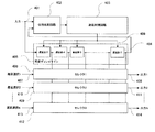
図5は、第二の実施形態における可変遅延回路517を用いた位相調整機能を持つ駆動パルス発生装置を示すブロック図である。図5に示すように、センサ駆動パルス1〜Nの遅延量は、駆動パルス発生装置外部より供給されるシリアル通信信号501、502、503をシリアル通信回路516で受信し、装置内の可変遅延回路517と同期化回路507、508、509にそれぞれ各駆動パルスの遅延制御信号と同期化制御信号を供給する。フリップフロップ510〜512のクロック端子には、可変遅延回路517が出力する3つの遅延クロック(上記遅延信号408、411、414)が入力される。
FIG. 5 is a block diagram showing a drive pulse generator having a phase adjustment function using the
図6は、図5に示した駆動パルス発生回路の詳細を示すブロック図である。また、図7(a)、図7(b)は、図6の駆動パルス発生回路の動作を示すタイミングチャートである。尚、図6は、以下の説明に必要な図5の一部のみを示す図である。 FIG. 6 is a block diagram showing details of the drive pulse generation circuit shown in FIG. FIGS. 7A and 7B are timing charts showing the operation of the drive pulse generation circuit of FIG. FIG. 6 is a diagram showing only a part of FIG. 5 necessary for the following description.
同期化回路509はマスタクロック506で同期化された信号Aを出力する。次に、任意の遅延をとり得る遅延クロック604の立ち上がりで動作するDフリップフロップ510のセットアップタイム、ホールドタイムを満足するために挿入されている。シリアル通信回路516は、排他的論理和素子603を利用して、設定された遅延量に応じて前段のDフリップフロップ602に供給するクロックを、マスタクロック506とマスタクロック506の反転クロックとのどちらか一方に制御する(エッジ設定)。すなわち、本実施形態では、エッジ設定は装置外部よりシリアル通信によって設定している。
The
本実施形態のように、遅延クロック604で同期化される前段のDフリップフロップ602において、マスタクロック506の正転・反転のいずれかで同期化することを切り替え可能とすることによって遅延クロック604がマスタクロック506に対して0度〜360度の遅延量(位相差)を持ったとしても、確実に遅延クロック604で同期化することが可能となる。図7(a)及び図7(b)は、エッジ設定に応じてセンサ駆動パルス1が変化することを示している。また、設定されたエッジ設定は遅延量が温度変動や電圧変動等の外部環境に依存しないことから、外部環境の変動によって設定を変更する必要はなく、遅延設定に対して一義的に決定することができる。
As in the present embodiment, in the preceding stage D flip-flop 602 synchronized with the delay clock 604, the synchronization can be switched by either normal rotation or inversion of the
以上説明したように、本実施形態の駆動パルス発生装置によれば、異なる遅延量を持つ複数のセンサ駆動パルスの相対的な位相関係は温度や電圧などの外部環境に依存しにくい構成である。例えば、本実施形態の駆動パルス発生装置により撮像素子を駆動する撮像装置であれば、外部環境の変動に影響されずに高品質な画素データを得ることができる。本実施形態の駆動パルス発生装置は、イメージャ(撮像素子)を駆動する駆動パルスを出力しているが、これに限定されるものではなく、ADコンバータに供給するADサンプリングパルスなどの制御信号を出力した場合にも、本実施形態と同様の効果が得られる。 As described above, according to the drive pulse generator of the present embodiment, the relative phase relationship between a plurality of sensor drive pulses having different delay amounts is less dependent on the external environment such as temperature and voltage. For example, an image pickup apparatus that drives an image pickup element using the drive pulse generator of this embodiment can obtain high-quality pixel data without being affected by fluctuations in the external environment. The drive pulse generator of this embodiment outputs a drive pulse for driving an imager (imaging device), but is not limited to this, and outputs a control signal such as an AD sampling pulse supplied to the AD converter. Even in this case, the same effect as the present embodiment can be obtained.
[第三の実施形態]
本発明の第三の実施形態に係る駆動パルス発生装置は、図5に示した第二の実施形態に係る駆動パルス発生装置と類似する実施形態であるが、可変遅延回路に供給される遅延設定情報から最適なエッジ選択信号を同期化回路に供給する同期化制御回路を設けた点が異なる。
[Third embodiment]
The drive pulse generator according to the third embodiment of the present invention is an embodiment similar to the drive pulse generator according to the second embodiment shown in FIG. 5, but the delay setting supplied to the variable delay circuit. The difference is that a synchronization control circuit for supplying an optimum edge selection signal from the information to the synchronization circuit is provided.
図8は、第三の実施形態における、可変遅延回路を用いた位相調整機能を持つ駆動パルス発生装置を示すブロック図である。センサ駆動パルス1〜Nの遅延量は、装置外部より供給されるシリアル通信信号701、702、703をシリアル通信回路716で受信し、装置内の可変遅延回路717と同期化制御回路718に供給される。同期化制御回路718では、可変遅延回路717に供給される遅延制御信号704にから最適な同期化制御信号を生成し、同期化回路708、709、710に供給する。
FIG. 8 is a block diagram showing a drive pulse generator having a phase adjustment function using a variable delay circuit in the third embodiment. As for the delay amount of the
図9は、図8の駆動パルス発生装置の詳細な構成及びエッジ設定例を示す図である。尚、図9は、図8の一部の構成のみを詳細に示している。同期化回路806はマスタクロック801で同期化された信号Aが、任意の遅延をとり得る遅延クロック802の立ち上がりで動作するDフリップフロップ809のセットアップタイム、ホールドタイムを満足するために挿入されている。
FIG. 9 is a diagram showing a detailed configuration and an edge setting example of the drive pulse generator of FIG. FIG. 9 shows only a part of the configuration of FIG. 8 in detail. The
設定された遅延量に応じて前段のDフリップフロップ808に供給されるクロックを、マスタクロック801とマスタクロック801の反転クロック802とのどちらか一方に選択する。本実施形態では、そのエッジ設定は、図8に示すように遅延設定に応じて同期化制御回路812より供給される。この同期化制御信号は可変遅延回路803に設定される遅延量に応じて自動的に変化し、例えば図9の下段に示すテーブルで示したような制御を行う。本実施形態のように、遅延クロック802で同期化される前段のDフリップフロップ808が、マスタクロック801の正転・反転のいずれかの切り替え機能を持たせることによって遅延クロック802がマスタクロック801に対して0度〜360度の遅延量(位相差)を持ったとしても、確実に遅延クロック802で同期化することが可能となる。
The clock supplied to the preceding D flip-
また、設定されたエッジ設定は遅延量が温度変動や電圧変動等の外部環境に依存しないことから、外部環境の変動によって設定を変更する必要はなく、遅延設定に対して一義的に決定することができる。 In addition, since the set edge settings do not depend on the external environment such as temperature fluctuations and voltage fluctuations, the delay setting does not need to be changed due to fluctuations in the external environment and should be determined uniquely with respect to the delay settings. Can do.
本実施形態の駆動パルス発生装置によれば、異なる遅延量を持つ複数のセンサ駆動パルスの相対的な位相関係は温度や電圧などの外部環境に依存しにくいため、外部環境に依らず高品質な画素データを得ることができる。本実施形態は、イメージャを駆動する駆動パルスに対して適応しているが、ADコンバータに供給するADサンプリングパルスなどの制御信号に本発明を適応することによっても同様の効果が得られる。 According to the drive pulse generation device of the present embodiment, the relative phase relationship between a plurality of sensor drive pulses having different delay amounts is less dependent on the external environment such as temperature and voltage, and therefore has high quality regardless of the external environment. Pixel data can be obtained. Although the present embodiment is adapted to the drive pulse for driving the imager, the same effect can be obtained by applying the present invention to a control signal such as an AD sampling pulse supplied to the AD converter.
[実施例1]
次に、図10を参照して、上記の第一〜第三の実施形態で示した駆動パルス発生装置を、撮像装置に適用した場合の実施例1について説明する。図10は、上記の第一〜第三の実施形態で示した駆動パルス発生装置を撮像装置である「スチルビデオカメラ」に適用した場合を示すブロック図である。尚、後述するタイミング発生部8に上記の第一〜第三の実施形態で示した駆動パルス発生装置が含まれている。
[Example 1]
Next, with reference to FIG. 10, Example 1 in the case where the drive pulse generator shown in the first to third embodiments is applied to an imaging device will be described. FIG. 10 is a block diagram showing a case where the drive pulse generator shown in the first to third embodiments is applied to a “still video camera” that is an imaging device. Note that the timing generator 8 described later includes the drive pulse generator shown in the first to third embodiments.
図10において、1はレンズのプロテクトとメインスイッチを兼ねるバリア、2は被写体の光学像を固体撮像素子4に結像させるレンズ、3はレンズ2を通った光量を可変するための絞り、4はレンズ2で結像された被写体を画像信号として取り込むための固体撮像素子、6は固体撮像素子4より出力される画像信号のアナログ−ディジタル変換を行うA/D変換器、7はA/D変換器6より出力された画像データに各種の補正を行ったりデータを圧縮する信号処理部、8は固体撮像素子4、撮像信号処理回路5、A/D変換器6、信号処理部7に、各種タイミング信号を出力するタイミング発生部、9は各種演算とスチルビデオカメラ全体を制御する全体制御・演算部、10は画像データを一時的に記憶する為のメモリ部、11は記録媒体に記録または読み出しを行うためのインターフェース部、12は画像データの記録または読み出しを行う為の半導体メモリ等の着脱可能な記録媒体、13は外部コンピュータ等と通信する為のインターフェース部である。
In FIG. 10, 1 is a barrier that serves as a lens protect and a main switch, 2 is a lens that forms an optical image of a subject on the solid-
次に、前述の構成における撮影時のスチルビデオカメラの動作について説明する。
バリア1がオープンされるとメイン電源がオンされ、次にコントロール系の電源がオンし、更にA/D変換器6などの撮像系回路の電源がオンされる。それから、露光量を制御する為に、全体制御・演算部9は絞り3を開放にし、固体撮像素子4から出力された信号はA/D変換器6で変換された後、信号処理部7に入力される。そのデータを基に露出の演算を全体制御・演算部9で行う。
Next, the operation of the still video camera at the time of shooting in the above configuration will be described.
When the
この測光を行った結果により明るさを判断し、その結果に応じて全体制御・演算部9は絞りを制御する。次に、固体撮像素子4から出力された信号をもとに、高周波成分を取り出し被写体までの距離の演算を全体制御・演算部9で行う。その後、レンズを駆動して合焦か否かを判断し、合焦していないと判断した時は、再びレンズを駆動し測距を行う。
そして、合焦が確認された後に本露光が始まる。
The brightness is determined based on the result of the photometry, and the overall control /
Then, after the in-focus state is confirmed, the main exposure starts.
露光が終了すると、固体撮像素子4から出力された画像信号はA/D変換器6でA/D変換され、信号処理部7を通り全体制御・演算部9によりメモリ部に書き込まれる。その後、メモリ部10に蓄積されたデータは、全体制御・演算部9の制御により記録媒体制御I/F部を通り半導体メモリ等の着脱可能な記録媒体12に記録される。また、外部I/F部13を通り直接コンピュータ等に入力して画像の加工を行ってもよい。
When the exposure is completed, the image signal output from the solid-state imaging device 4 is A / D converted by the A /
[実施例2]
次に、図11を参照して、上記の第一〜第三の実施形態で示した駆動パルス発生装置を、撮像装置に適用した場合の実施例2について説明する。図11は、上記の第一〜第三の実施形態で示した駆動パルス発生装置を撮像装置である「ビデオカメラ」に適用した場合を示すブロック図である。尚、後述する固体撮像素子3やサンプルホールド回路4に対して上記の第一〜第三の実施形態で示した駆動パルス発生装置が制御パルスを発信する構成である。ここでは、特に図11に上記の第一〜第三の実施形態で示した駆動パルス発生装置を示していない。
[Example 2]
Next, with reference to FIG. 11, Example 2 in the case where the drive pulse generator shown in the first to third embodiments is applied to an imaging device will be described. FIG. 11 is a block diagram showing a case where the drive pulse generator shown in the first to third embodiments is applied to a “video camera” that is an imaging device. Note that the drive pulse generator shown in the first to third embodiments transmits a control pulse to a solid-
図11において、1は撮影レンズで焦点調節を行うためのフォーカスレンズ1A、ズーム動作を行うズームレンズ1B、結像用のレンズ1Cを備えている。2は絞り、3は撮像面に結像された被写体像を光電変換して電気的な撮像信号に変換する固体撮像素子、4は固体撮像素子3より出力された撮像信号をサンプルホールドし、さらに、レベルをアンプするサンプルホールド回路(S/H回路)であり、映像信号を出力する。
In FIG. 11,
5はサンプルホールド回路4から出力された映像信号にガンマ補正、色分離、ブランキング処理等の所定の処理を施すプロセス回路で、輝度信号Yおよびクロマ信号Cを出力する。プロセス回路5から出力されたクロマ信号Cは、色信号補正回路21で、ホワイトバランス及び色バランスの補正がなされ、色差信号R−Y,B−Yとして出力される。
A
また、プロセス回路5から出力された輝度信号Yと、色信号補正回路21から出力された色差信号R−Y,B−Yは、エンコーダ回路(ENC回路)24で変調され、標準テレビジョン信号として出力される。そして、図示しないビデオレコーダ、あるいは電子ビューファインダ等のモニタEVFへと供給される。
Also, the luminance signal Y output from the
次いで、6はアイリス制御回路で有り、サンプルホールド回路4から供給される映像信号に基づいてアイリス駆動回路7を制御し、映像信号のレベルが所定レベルの一定値となるように、絞り2の開口量を制御すべくigメータを自動制御するものである。
Next,
13、14は、サンプルホールド回路4から出力された映像信号中より合焦検出を行うために必要な高周波成分を抽出する異なった帯域制限のバンドパスフィルタ(BPF)である。第一のバンドパスフィルタ13(BPF1)、及び第二のバンドパスフィルタ14(BPF2)から出力された信号は、ゲート回路15及びフォーカスゲート枠信号で各々でゲートされ、ピーク検出回路16でピーク値が検出されてホールドされると共に、論理制御回路17に入力される。
この信号を焦点電圧と呼び、この焦点電圧によってフォーカスを合わせている。また、18はフォーカスレンズ1Aの移動位置を検出するフォーカスエンコーダ、19はズームレンズ1Bの焦点距離を検出するズームエンコーダ、20は絞り2の開口量を検出するアイリスエンコーダである。これらのエンコーダの検出値は、システムコントロールを行う論理制御回路17へと供給される。
This signal is called a focus voltage, and the focus is adjusted by this focus voltage.
論理制御回路17は、設定された合焦検出領域内に相当する映像信号に基づいて、被写体に対する合焦検出を行い焦点調節を行う。即ち、各々のバンドパスフィルタ13、14より供給された高周波成分のピーク値情報を取り込み、高周波成分のピーク値が最大となる位置へとフォーカスレンズ1Aを駆動すべくフォーカス駆動回路9にフォーカスモータ10の回転方向、回転速度、回転/停止等の制御信号を供給し、これを制御する。
The logic control circuit 17 performs focus detection by performing focus detection on the subject based on a video signal corresponding to the set focus detection area. That is, the peak value information of the high frequency components supplied from the respective band pass filters 13 and 14 is taken in, and the
以上、この発明の実施形態について図面を参照して詳述してきたが、具体的な構成はこの実施形態に限られるものではなく、この発明の要旨を逸脱しない範囲の設計等も含まれる。 The embodiment of the present invention has been described in detail with reference to the drawings. However, the specific configuration is not limited to this embodiment, and includes designs and the like that do not depart from the gist of the present invention.
101、506、706、801・・・マスタクロック
102、517、718、803・・・可変遅延回路
103、407、410、413、504、704・・・遅延選択信号
104、604、802・・・遅延クロック
105、707、805・・・タイミング発生回路
106・・・内部信号
107、109、510、511、512、601、602、711、712、713、807、808、809・・・Dフリップフロップ
108、513、514、515、714、715、716、811、1011、1201、1206、1211・・・センサ駆動パルス
401・・・入力信号
202、402・・・位相比較回路
203、403・・・遅延制御回路
204、404・・・遅延素子
205、405・・・可変ディレイライン
206、406、409、412・・・セレクタ
408、411、414・・・出力信号
209、409・・・遅延制御信号
501、701・・・チップセレクト
502、702・・・シリアルクロック
503、703・・・シリアルデータ
505、705、・・・同期化制御信号
507、508、509、708、709、710、806・・・同期化回路
515、717、804・・・シリアル通信回路
603、810・・・EXORゲート
718、812・・・同期化制御回路
101, 506, 706, 801... Master clocks 102, 517, 718, 803...
Claims (6)
前記クロックと前記遅延手段の出力との位相差を検出する位相比較手段と、
前記位相比較手段が検出した前記位相差に応じて遅延量を制御するための前記制御信号を前記遅延手段へ出力する遅延制御手段と、
前記遅延素子のいずれか一つの出力信号を選択して遅延クロックを出力する選択出力手段と、
前記入力されるクロックに同期した信号を生成するタイミング発生回路と、
前記タイミング発生回路が生成した信号を前記入力されるクロックに同期化して信号を出力するフリップフロップを具備する複数の同期化回路と、
前記複数の同期化回路がそれぞれ出力した信号を前記遅延クロックに同期化させたパルス信号を出力する複数の同期出力手段と、
前記フリップフロップに供給する信号のクロックを制御するエッジ設定手段と
を具備することを特徴とするパルス生成回路。 A delay unit configured by connecting a plurality of delay elements in series and delaying an input clock by a delay amount according to a control signal; and
Phase comparison means for detecting a phase difference between the clock and the output of the delay means;
Delay control means for outputting the control signal for controlling the delay amount according to the phase difference detected by the phase comparison means to the delay means;
Selection output means for selecting any one output signal of the delay elements and outputting a delay clock;
A timing generation circuit for generating a signal synchronized with the input clock;
A plurality of synchronization circuits comprising flip-flops for synchronizing the signal generated by the timing generation circuit with the input clock and outputting the signal;
A plurality of synchronization output means for outputting a pulse signal obtained by synchronizing a signal output from each of the plurality of synchronization circuits with the delay clock ;
An edge setting means for controlling a clock of a signal supplied to the flip-flop .
前記撮像素子が出力する信号をAD変換する変換手段と、Conversion means for AD converting a signal output from the image sensor;
請求項1乃至4のいずれか1項に記載のパルス生成回路とA pulse generation circuit according to any one of claims 1 to 4,
を具備し、Comprising
前記パルス生成回路は、前記撮像素子及び前記変換手段の少なくとも一方に前記パルス信号を出力することを特徴とする撮像装置。The image pickup apparatus, wherein the pulse generation circuit outputs the pulse signal to at least one of the image pickup device and the conversion unit.
前記撮像素子へ光を結像する光学系とを具備することを特徴とするカメラ。An optical system for imaging light onto the image sensor.
Priority Applications (1)
| Application Number | Priority Date | Filing Date | Title |
|---|---|---|---|
| JP2005054136A JP4227596B2 (en) | 2005-02-28 | 2005-02-28 | Pulse generation circuit, imaging device and camera |
Applications Claiming Priority (1)
| Application Number | Priority Date | Filing Date | Title |
|---|---|---|---|
| JP2005054136A JP4227596B2 (en) | 2005-02-28 | 2005-02-28 | Pulse generation circuit, imaging device and camera |
Publications (2)
| Publication Number | Publication Date |
|---|---|
| JP2006245632A JP2006245632A (en) | 2006-09-14 |
| JP4227596B2 true JP4227596B2 (en) | 2009-02-18 |
Family
ID=37051624
Family Applications (1)
| Application Number | Title | Priority Date | Filing Date |
|---|---|---|---|
| JP2005054136A Expired - Fee Related JP4227596B2 (en) | 2005-02-28 | 2005-02-28 | Pulse generation circuit, imaging device and camera |
Country Status (1)
| Country | Link |
|---|---|
| JP (1) | JP4227596B2 (en) |
Families Citing this family (2)
| Publication number | Priority date | Publication date | Assignee | Title |
|---|---|---|---|---|
| JP2008206763A (en) * | 2007-02-27 | 2008-09-11 | Olympus Corp | Clock supply circuit and electronic endoscope system |
| JP6334946B2 (en) * | 2014-02-19 | 2018-05-30 | キヤノン株式会社 | Imaging apparatus and control method thereof |
-
2005
- 2005-02-28 JP JP2005054136A patent/JP4227596B2/en not_active Expired - Fee Related
Also Published As
| Publication number | Publication date |
|---|---|
| JP2006245632A (en) | 2006-09-14 |
Similar Documents
| Publication | Publication Date | Title |
|---|---|---|
| KR100666290B1 (en) | Image pick up device and image pick up method | |
| JP3664123B2 (en) | Imaging apparatus and image quality correction method | |
| WO2010001517A1 (en) | Still image and dynamic image capturing device | |
| JP2007020156A (en) | Imaging apparatus and imaging system | |
| US7880789B2 (en) | Solid-state image pick-up apparatus capable of remarkably reducing dark current and a drive method therefor | |
| JP4616429B2 (en) | Image processing device | |
| US20090021628A1 (en) | Ccd solid-state imaging device, drive method thereof and imaging apparatus | |
| JP4298685B2 (en) | Shift register, and solid-state imaging device and camera using the shift register | |
| CN101931745A (en) | Digital camera apparatus | |
| JP4227596B2 (en) | Pulse generation circuit, imaging device and camera | |
| JP4724400B2 (en) | Imaging device | |
| JP2007134806A (en) | Solid-state imaging element | |
| JP4745677B2 (en) | Imaging device | |
| JP5340374B2 (en) | Imaging apparatus and imaging system | |
| JP3777901B2 (en) | Video information processing device | |
| JP2009105852A (en) | Video signal processing device, solid-state imaging apparatus and electronic information device | |
| JP2007110639A (en) | Solid-state imaging element, drive method thereof, and imaging apparatus | |
| JP2005286470A (en) | Imaging unit | |
| JP2007074363A (en) | Imaging apparatus | |
| JP2010062902A (en) | Pulse phase adjusting device for imaging apparatus, method of manufacturing imaging apparatus, and imaging apparatus | |
| JP4824467B2 (en) | Solid-state imaging device | |
| JP4401858B2 (en) | Imaging device | |
| JP6334946B2 (en) | Imaging apparatus and control method thereof | |
| JP2007036332A (en) | Imaging apparatus and drive method thereof | |
| JP4810566B2 (en) | Imaging device |
Legal Events
| Date | Code | Title | Description |
|---|---|---|---|
| A977 | Report on retrieval |
Free format text: JAPANESE INTERMEDIATE CODE: A971007 Effective date: 20080131 |
|
| A131 | Notification of reasons for refusal |
Free format text: JAPANESE INTERMEDIATE CODE: A131 Effective date: 20080219 |
|
| A521 | Request for written amendment filed |
Free format text: JAPANESE INTERMEDIATE CODE: A523 Effective date: 20080418 |
|
| A131 | Notification of reasons for refusal |
Free format text: JAPANESE INTERMEDIATE CODE: A131 Effective date: 20080826 |
|
| A521 | Request for written amendment filed |
Free format text: JAPANESE INTERMEDIATE CODE: A523 Effective date: 20081027 |
|
| TRDD | Decision of grant or rejection written | ||
| A01 | Written decision to grant a patent or to grant a registration (utility model) |
Free format text: JAPANESE INTERMEDIATE CODE: A01 Effective date: 20081125 |
|
| A01 | Written decision to grant a patent or to grant a registration (utility model) |
Free format text: JAPANESE INTERMEDIATE CODE: A01 |
|
| A61 | First payment of annual fees (during grant procedure) |
Free format text: JAPANESE INTERMEDIATE CODE: A61 Effective date: 20081128 |
|
| FPAY | Renewal fee payment (event date is renewal date of database) |
Free format text: PAYMENT UNTIL: 20111205 Year of fee payment: 3 |
|
| R150 | Certificate of patent or registration of utility model |
Ref document number: 4227596 Country of ref document: JP Free format text: JAPANESE INTERMEDIATE CODE: R150 Free format text: JAPANESE INTERMEDIATE CODE: R150 |
|
| FPAY | Renewal fee payment (event date is renewal date of database) |
Free format text: PAYMENT UNTIL: 20121205 Year of fee payment: 4 |
|
| FPAY | Renewal fee payment (event date is renewal date of database) |
Free format text: PAYMENT UNTIL: 20131205 Year of fee payment: 5 |
|
| LAPS | Cancellation because of no payment of annual fees |