JP4209097B2 - Semiconductor photo detector - Google Patents
Semiconductor photo detector Download PDFInfo
- Publication number
- JP4209097B2 JP4209097B2 JP2001266930A JP2001266930A JP4209097B2 JP 4209097 B2 JP4209097 B2 JP 4209097B2 JP 2001266930 A JP2001266930 A JP 2001266930A JP 2001266930 A JP2001266930 A JP 2001266930A JP 4209097 B2 JP4209097 B2 JP 4209097B2
- Authority
- JP
- Japan
- Prior art keywords
- layer
- receiving element
- conductive layer
- light receiving
- underlayer
- Prior art date
- Legal status (The legal status is an assumption and is not a legal conclusion. Google has not performed a legal analysis and makes no representation as to the accuracy of the status listed.)
- Expired - Lifetime
Links
- 239000004065 semiconductor Substances 0.000 title claims description 137
- 239000010410 layer Substances 0.000 claims description 253
- 150000004767 nitrides Chemical class 0.000 claims description 59
- 239000000758 substrate Substances 0.000 claims description 50
- 239000013078 crystal Substances 0.000 claims description 37
- 229910052594 sapphire Inorganic materials 0.000 claims description 23
- 239000010980 sapphire Substances 0.000 claims description 23
- 238000004519 manufacturing process Methods 0.000 claims description 14
- 238000005121 nitriding Methods 0.000 claims description 13
- 238000002488 metal-organic chemical vapour deposition Methods 0.000 claims description 10
- 238000000034 method Methods 0.000 claims description 6
- 239000002344 surface layer Substances 0.000 claims description 2
- 238000010586 diagram Methods 0.000 description 10
- 239000007789 gas Substances 0.000 description 8
- 238000001514 detection method Methods 0.000 description 7
- QGZKDVFQNNGYKY-UHFFFAOYSA-N Ammonia Chemical compound N QGZKDVFQNNGYKY-UHFFFAOYSA-N 0.000 description 6
- IJGRMHOSHXDMSA-UHFFFAOYSA-N Atomic nitrogen Chemical compound N#N IJGRMHOSHXDMSA-UHFFFAOYSA-N 0.000 description 6
- 229910002704 AlGaN Inorganic materials 0.000 description 5
- 230000015572 biosynthetic process Effects 0.000 description 5
- 230000035945 sensitivity Effects 0.000 description 5
- 230000000052 comparative effect Effects 0.000 description 4
- 229910000069 nitrogen hydride Inorganic materials 0.000 description 4
- 238000010438 heat treatment Methods 0.000 description 3
- 229910052757 nitrogen Inorganic materials 0.000 description 3
- 229910001218 Gallium arsenide Inorganic materials 0.000 description 2
- 239000000654 additive Substances 0.000 description 2
- 230000000996 additive effect Effects 0.000 description 2
- 230000000694 effects Effects 0.000 description 2
- 239000000463 material Substances 0.000 description 2
- 230000003287 optical effect Effects 0.000 description 2
- 239000002994 raw material Substances 0.000 description 2
- UFHFLCQGNIYNRP-UHFFFAOYSA-N Hydrogen Chemical compound [H][H] UFHFLCQGNIYNRP-UHFFFAOYSA-N 0.000 description 1
- 229910010093 LiAlO Inorganic materials 0.000 description 1
- 229910010936 LiGaO2 Inorganic materials 0.000 description 1
- 229910026161 MgAl2O4 Inorganic materials 0.000 description 1
- 238000004833 X-ray photoelectron spectroscopy Methods 0.000 description 1
- 229910007948 ZrB2 Inorganic materials 0.000 description 1
- 229910021529 ammonia Inorganic materials 0.000 description 1
- 238000004458 analytical method Methods 0.000 description 1
- 239000000969 carrier Substances 0.000 description 1
- 239000012159 carrier gas Substances 0.000 description 1
- 238000004140 cleaning Methods 0.000 description 1
- 238000000151 deposition Methods 0.000 description 1
- 230000008021 deposition Effects 0.000 description 1
- 238000005530 etching Methods 0.000 description 1
- 239000001257 hydrogen Substances 0.000 description 1
- 229910052739 hydrogen Inorganic materials 0.000 description 1
- 239000012535 impurity Substances 0.000 description 1
- WPYVAWXEWQSOGY-UHFFFAOYSA-N indium antimonide Chemical compound [Sb]#[In] WPYVAWXEWQSOGY-UHFFFAOYSA-N 0.000 description 1
- QJGQUHMNIGDVPM-UHFFFAOYSA-N nitrogen group Chemical group [N] QJGQUHMNIGDVPM-UHFFFAOYSA-N 0.000 description 1
- 229910052596 spinel Inorganic materials 0.000 description 1
- 230000002195 synergetic effect Effects 0.000 description 1
- 235000013619 trace mineral Nutrition 0.000 description 1
- 239000011573 trace mineral Substances 0.000 description 1
- 230000007704 transition Effects 0.000 description 1
Images


Classifications
-
- H—ELECTRICITY
- H01—ELECTRIC ELEMENTS
- H01L—SEMICONDUCTOR DEVICES NOT COVERED BY CLASS H10
- H01L31/00—Semiconductor devices sensitive to infrared radiation, light, electromagnetic radiation of shorter wavelength or corpuscular radiation and specially adapted either for the conversion of the energy of such radiation into electrical energy or for the control of electrical energy by such radiation; Processes or apparatus specially adapted for the manufacture or treatment thereof or of parts thereof; Details thereof
- H01L31/18—Processes or apparatus specially adapted for the manufacture or treatment of these devices or of parts thereof
- H01L31/184—Processes or apparatus specially adapted for the manufacture or treatment of these devices or of parts thereof the active layers comprising only AIIIBV compounds, e.g. GaAs, InP
- H01L31/1852—Processes or apparatus specially adapted for the manufacture or treatment of these devices or of parts thereof the active layers comprising only AIIIBV compounds, e.g. GaAs, InP comprising a growth substrate not being an AIIIBV compound
-
- H—ELECTRICITY
- H01—ELECTRIC ELEMENTS
- H01L—SEMICONDUCTOR DEVICES NOT COVERED BY CLASS H10
- H01L21/00—Processes or apparatus adapted for the manufacture or treatment of semiconductor or solid state devices or of parts thereof
- H01L21/02—Manufacture or treatment of semiconductor devices or of parts thereof
- H01L21/02104—Forming layers
- H01L21/02365—Forming inorganic semiconducting materials on a substrate
- H01L21/02367—Substrates
- H01L21/0237—Materials
- H01L21/0242—Crystalline insulating materials
-
- H—ELECTRICITY
- H01—ELECTRIC ELEMENTS
- H01L—SEMICONDUCTOR DEVICES NOT COVERED BY CLASS H10
- H01L21/00—Processes or apparatus adapted for the manufacture or treatment of semiconductor or solid state devices or of parts thereof
- H01L21/02—Manufacture or treatment of semiconductor devices or of parts thereof
- H01L21/02104—Forming layers
- H01L21/02365—Forming inorganic semiconducting materials on a substrate
- H01L21/02436—Intermediate layers between substrates and deposited layers
- H01L21/02439—Materials
- H01L21/02455—Group 13/15 materials
- H01L21/02458—Nitrides
-
- H—ELECTRICITY
- H01—ELECTRIC ELEMENTS
- H01L—SEMICONDUCTOR DEVICES NOT COVERED BY CLASS H10
- H01L21/00—Processes or apparatus adapted for the manufacture or treatment of semiconductor or solid state devices or of parts thereof
- H01L21/02—Manufacture or treatment of semiconductor devices or of parts thereof
- H01L21/02104—Forming layers
- H01L21/02365—Forming inorganic semiconducting materials on a substrate
- H01L21/02518—Deposited layers
- H01L21/02521—Materials
- H01L21/02538—Group 13/15 materials
- H01L21/0254—Nitrides
-
- H—ELECTRICITY
- H01—ELECTRIC ELEMENTS
- H01L—SEMICONDUCTOR DEVICES NOT COVERED BY CLASS H10
- H01L31/00—Semiconductor devices sensitive to infrared radiation, light, electromagnetic radiation of shorter wavelength or corpuscular radiation and specially adapted either for the conversion of the energy of such radiation into electrical energy or for the control of electrical energy by such radiation; Processes or apparatus specially adapted for the manufacture or treatment thereof or of parts thereof; Details thereof
- H01L31/0248—Semiconductor devices sensitive to infrared radiation, light, electromagnetic radiation of shorter wavelength or corpuscular radiation and specially adapted either for the conversion of the energy of such radiation into electrical energy or for the control of electrical energy by such radiation; Processes or apparatus specially adapted for the manufacture or treatment thereof or of parts thereof; Details thereof characterised by their semiconductor bodies
- H01L31/0256—Semiconductor devices sensitive to infrared radiation, light, electromagnetic radiation of shorter wavelength or corpuscular radiation and specially adapted either for the conversion of the energy of such radiation into electrical energy or for the control of electrical energy by such radiation; Processes or apparatus specially adapted for the manufacture or treatment thereof or of parts thereof; Details thereof characterised by their semiconductor bodies characterised by the material
- H01L31/0264—Inorganic materials
- H01L31/0304—Inorganic materials including, apart from doping materials or other impurities, only AIIIBV compounds
-
- H—ELECTRICITY
- H01—ELECTRIC ELEMENTS
- H01L—SEMICONDUCTOR DEVICES NOT COVERED BY CLASS H10
- H01L31/00—Semiconductor devices sensitive to infrared radiation, light, electromagnetic radiation of shorter wavelength or corpuscular radiation and specially adapted either for the conversion of the energy of such radiation into electrical energy or for the control of electrical energy by such radiation; Processes or apparatus specially adapted for the manufacture or treatment thereof or of parts thereof; Details thereof
- H01L31/08—Semiconductor devices sensitive to infrared radiation, light, electromagnetic radiation of shorter wavelength or corpuscular radiation and specially adapted either for the conversion of the energy of such radiation into electrical energy or for the control of electrical energy by such radiation; Processes or apparatus specially adapted for the manufacture or treatment thereof or of parts thereof; Details thereof in which radiation controls flow of current through the device, e.g. photoresistors
- H01L31/10—Semiconductor devices sensitive to infrared radiation, light, electromagnetic radiation of shorter wavelength or corpuscular radiation and specially adapted either for the conversion of the energy of such radiation into electrical energy or for the control of electrical energy by such radiation; Processes or apparatus specially adapted for the manufacture or treatment thereof or of parts thereof; Details thereof in which radiation controls flow of current through the device, e.g. photoresistors characterised by at least one potential-jump barrier or surface barrier, e.g. phototransistors
- H01L31/101—Devices sensitive to infrared, visible or ultraviolet radiation
- H01L31/102—Devices sensitive to infrared, visible or ultraviolet radiation characterised by only one potential barrier or surface barrier
- H01L31/105—Devices sensitive to infrared, visible or ultraviolet radiation characterised by only one potential barrier or surface barrier the potential barrier being of the PIN type
-
- H—ELECTRICITY
- H01—ELECTRIC ELEMENTS
- H01L—SEMICONDUCTOR DEVICES NOT COVERED BY CLASS H10
- H01L33/00—Semiconductor devices with at least one potential-jump barrier or surface barrier specially adapted for light emission; Processes or apparatus specially adapted for the manufacture or treatment thereof or of parts thereof; Details thereof
- H01L33/005—Processes
- H01L33/0062—Processes for devices with an active region comprising only III-V compounds
- H01L33/0066—Processes for devices with an active region comprising only III-V compounds with a substrate not being a III-V compound
- H01L33/007—Processes for devices with an active region comprising only III-V compounds with a substrate not being a III-V compound comprising nitride compounds
-
- Y—GENERAL TAGGING OF NEW TECHNOLOGICAL DEVELOPMENTS; GENERAL TAGGING OF CROSS-SECTIONAL TECHNOLOGIES SPANNING OVER SEVERAL SECTIONS OF THE IPC; TECHNICAL SUBJECTS COVERED BY FORMER USPC CROSS-REFERENCE ART COLLECTIONS [XRACs] AND DIGESTS
- Y02—TECHNOLOGIES OR APPLICATIONS FOR MITIGATION OR ADAPTATION AGAINST CLIMATE CHANGE
- Y02E—REDUCTION OF GREENHOUSE GAS [GHG] EMISSIONS, RELATED TO ENERGY GENERATION, TRANSMISSION OR DISTRIBUTION
- Y02E10/00—Energy generation through renewable energy sources
- Y02E10/50—Photovoltaic [PV] energy
- Y02E10/544—Solar cells from Group III-V materials
-
- Y—GENERAL TAGGING OF NEW TECHNOLOGICAL DEVELOPMENTS; GENERAL TAGGING OF CROSS-SECTIONAL TECHNOLOGIES SPANNING OVER SEVERAL SECTIONS OF THE IPC; TECHNICAL SUBJECTS COVERED BY FORMER USPC CROSS-REFERENCE ART COLLECTIONS [XRACs] AND DIGESTS
- Y02—TECHNOLOGIES OR APPLICATIONS FOR MITIGATION OR ADAPTATION AGAINST CLIMATE CHANGE
- Y02E—REDUCTION OF GREENHOUSE GAS [GHG] EMISSIONS, RELATED TO ENERGY GENERATION, TRANSMISSION OR DISTRIBUTION
- Y02E10/00—Energy generation through renewable energy sources
- Y02E10/50—Photovoltaic [PV] energy
- Y02E10/548—Amorphous silicon PV cells
Description
【0001】
【発明の属する技術分野】
本発明は、半導体受光素子の製造方法に関し、詳しくはフォトダイオードなどとして好適に用いることのできる半導体受光素子の製造方法に関する。
【0002】
【従来の技術】
近年においては、自動制御器、光計測器、光通信のみならず、テレビ、ビデオ、ステレオ、エアコンなどの日用品の中にも、光検出器としてのフォトダイオードなどの半導体受光素子が組み込まれている。このような半導体受光素子としては、直接遷移型で大きなバンド間ギャップを有するとともに、組成制御によってバンド間ギャップを自在に変化させることができることから、Ga系の窒化物半導体が用いられていた。
【0003】
図1は、従来のいわゆるPIN型の半導体受光素子の一例を示す構成図である。
【0004】
図1に示す半導体受光素子10においては、サファイア、ZnO、SiC、Si、GaAs、及びGaNなどの単結晶からなる基板1上において、AlNからなるバッファ層6、i−GaNからなる下地層2、n−AlGaNからなるn型導電層3、i−AlGaNからなる受光層4、p−GaNからなるp型導電層5がこの順に形成されている。n型導電層3の一部は露出しており、この露出した部分にAl/Tiなどのn型電極7が形成されるとともに、p型導電層5上にはAu/Niなどのp型電極8が形成されている。
【0005】
そして、半導体受光素子10に対して検出すべきカットオフ波長以下の波長の光が入射すると、この光によって受光層4が励起され、n型電極7及びp型電極8を介して、半導体受光素子10を含む所定の電気回路中を所定の電流が流れるようになる。そして、この電流を検出することによって前記受光した光を検出するように構成されている。
【0006】
【発明が解決しようとする課題】
図1に示す半導体受光素子10において、バッファ層6は、基板1と下地層2との格子定数差を補完して、基板1上に下地層2や導電層3及び5、受光層4をエピタキシャル成長させるべく、緩衝層としての作用を果たすものである。したがって、通常はその結晶性を無視して500〜700℃の低温において、アモルファス状に形成される。
【0007】
この結果、バッファ層6中には比較的多量の転位が含有されてしまい、この転位の一部が貫通転位として下地層2、n型導電層3、受光層4及びp型導電層5中に伝搬する。結果としてこれらの層中にも1010/cm2を超える量の転位が含まれていまい、結晶性が劣化してしまっていた。特に、短波長用の半導体受光素子、すなわちn型導電層3及び受光層4がAlをより多く含む場合において上記傾向は顕著になる。
【0008】
このような高転位で低結晶性の層から半導体受光素子を構成すると、各層の転位を通じていわゆる比較的大きな暗電流が流れることになる。したがって、前記半導体受光素子に光を入射させ、受光層を励起して得た電流を検出した場合に、検出電流の誤差が前記暗電流に起因して大きくなってしまい、S/N比あるいは検出感度が著しく劣化してしまうという問題があった。
【0009】
本発明は、暗電流を低減し、高い検出感度を有する半導体受光素子を提供することを目的とする。
【0010】
【課題を解決するための手段】
上記目的を達成すべく、本発明の受光素子構造の製造方法は、サファイア単結晶基板上にMOCVD法を用いて窒化物半導体からなる受光素子構造を製造する方法であって、前記サファイア単結晶基板に表面窒化処理を施す第1の工程と、表面窒化処理を施したサファイア単結晶基板を1100℃以上に昇温し、転位密度が1011/cm2以下であり、Al含有量が50原子%以上である窒化物半導体からなる膜厚が0.5〜3μmの下地層を形成する第2の工程と、前記下地層上に、転位密度が下地層よりも少なくかつ1010/cm2以下であり、前記下地層を構成する窒化物半導体よりも少ない含有量でAlを含む受光素子構造を構成する窒化物半導体層群を形成する第3の工程とを有することを特徴とする。
【0011】
本発明者らは、上記目的を達成するべく鋭意検討を実施した。上述した暗電流は、半導体受光素子を構成する各層の低結晶性に基づく高転位の結果として生じるものであることから、本発明者らは、半導体受光素子を構成する各層の転位量を減らして結晶性を向上させることを試みた。
【0012】
上述したように、半導体受光素子を構成する各層中における転位は、低結晶性のバッファ層に起因するものである。しかしながら、図1に示す従来の半導体受光素子においては、基板1としてはサファイア単結晶が用いられ、下地層2としてはGaNが用いられていたため、下地層上に形成した導電層に転位が貫通してしまうという問題があった。特に、Alを含む導電層を成膜するとその界面で転位が増加し、さらにはクラックを発生させてしまうという問題もあった。これは、導電層がAlを含むことによってその格子定数が縮小されるため、導電層内に引張応力が発生することに起因する。
【0013】
そこで、バッファ層のみならず、下地層についても種々検討を行った。図1に示す従来の半導体受光素子においては、その構成から明らかなように、導電層及び受光層ともにGaを主とした窒化物半導体から構成されている。したがって、これら各層に対する下地層についてもGa系を主とした、例えばGaNから構成することが当然と考えられていた。その結果、基板との格子不整合が生じ、これを緩和するために低温形成のバッファ層が必要とされていた。
【0014】
しかしながら、本発明者らは、当然と思われていた下地層の組成に着目し、この組成を変化させることを試みた。その結果、下地層を低転位で大きな結晶性のAlを主とする窒化物半導体から構成することを想到した。この下地層はバッファ層が存在しない場合においても、サファイアなどの基板上に大きな格子定数差を補完してエピタキシャル成長することができる。また、下地層の高い結晶性に基づいて、下地層上に形成された導電層及び受光層の結晶性も改善され、それらの転位量が低減される。
【0015】
結果として、半導体受光素子を構成する各層中に転位量が低減され、高い転位量に基づく高い暗電流の生成を効果的に抑制することができる。このため、暗電流に基づく検出電流値の誤差が低減され、前記半導体受光素子の検出感度を向上させることができる。
【0016】
【発明の実施の形態】
以下、本発明を発明の実施の形態に即して詳細に説明する。
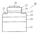
図2は、本発明の半導体受光素子の一例を示す構成図である。
図2に示す半導体受光素子20は、基板11上において、下地層12、n型導電層13、受光層14、p型導電層15を順次具えている。そして、図1に示す従来の半導体受光素子10と同様に、p型導電層15上には例えばAu/Niからなるp型電極18を有しており、n型導電層13の露出した部分においては例えばAl/Tiからなるn型電極17を有し、PIN型の半導体受光素子を構成している。
【0017】
図2において、n型導電層13、受光層14、p型導電層15は半導体受光素子における窒化物半導体層群を構成し、この窒化物半導体層群と、n型電極17及びp型電極18とから受光素子構造が構成される。
【0018】
下地層12は、本発明にしたがって、Alを含み、転位密度が1011/cm2以下の窒化物半導体から構成されていることが必要であり、さらには1010/cm2以下であることが好ましい。この場合においては、基板11との格子定数差を補完して、自らエピタキシャル成長されることができるとともに、その結果、下地層12上においてn型導電層13、受光層14、及びp型導電層15をもエピタキシャル成長させることができる。
【0019】
また、窒化物半導体層群を構成するn型導電層13、受光層14、及びp型導電層15は、下地層2よりも少ない含有量でAlを含み、転位密度が1010/cm2以下の窒化物半導体から構成されていることが必要である。これによって、半導体受光素子20の暗電流を効果的に抑制することができる。
【0020】
これは、下地層12とn型導電層13との間のAl組成差に起因して貫通転位の割合が減少し、n型導電層13、受光層14、及びp型導電層15中の転位密度を低減することができ、これによって、n型導電層13などの結晶性が向上するためである。
【0021】
上述した効果は、下地層12を構成する前記窒化物半導体におけるAlの含有量が多いほど、具体的には50原子%以上で顕著になる。特に、下地層12を構成する前記窒化物半導体は、AlNから構成することが好ましい。
【0022】
このように、下地層12を上述した高Al含有量の窒化物半導体から構成することによって、n型導電層13の結晶性をさらに向上させることができる。その結果、下地層12上に形成されたn型導電層13、受光層14、及びp型導電層15の結晶性を向上させて、さらなる低転位化を達成することもできる。
【0023】
例えば、下地層12がAlNから構成され、下地層12上に直接的に形成されたn型導電層13がGaを比較的多く含有するAlGaNなどから構成される場合などにおいては、下地層12とn型導電層13との間の組成差が増大するために、下地層12の転位量に比較してn型導電層13の転位量をより低減することができる。例えば、109/cm2以下の転位密度を比較的簡易に得ることができ、現状においては1×108/cm2まで転位密度を低減することができる。
【0024】
この結果、n型導電層13上に形成された受光層14及びp型導電層15中の転位量も当然に低減され、これらの層中においてもその転位密度を109/cm2以下にまで比較的簡易に低減することができる。さらに、現状においては、1×108/cm2まで低減することができる。
【0025】
Alを含み、低転位密度の高結晶性の窒化物半導体からなる下地層12は、例えば、MOCVD法により、その成膜温度を制御することによって得ることができる。具体的には、成膜温度を1100℃以上、好ましくは1250℃以下に設定することによって、目的とする高結晶性の窒化物半導体からなる下地層12を簡易に得ることができる。なお、本特許の成膜温度は、基板温度を意味する。
【0026】
なお、結晶性向上の観点から、下地層12の膜厚は大きいほど好ましいが、膜厚が大きくなり過ぎるとクラックの発生や剥離などが生じる。したがって、下地層12の膜厚は0.5〜3μmとし、さらには1〜3μmであることが好ましい。
【0027】
このような低転位密度で高い結晶性のn型導電層13などは、前述したような低転位で高結晶性の下地層12上に、例えばMOCVD法などによってエピタキシャル成長させることにより、必然的に得ることができる。
【0028】
基板11は、サファイア単結晶、ZnO単結晶、LiAlO2単結晶、LiGaO2単結晶、MgAl2O4単結晶、MgO単結晶などの酸化物単結晶、Si単結晶、SiC単結晶などのIV族あるいはIV−IV族単結晶、GaAs単結晶、AlN単結晶、GaN単結晶、及びAlGaN単結晶などのIII−V族単結晶、ZrB2などのホウ化物単結晶などの、公知の基板材料から構成することができるが、本発明では、サファイア単結晶基板を用いる。
【0029】
本発明では、サファイア単結晶基板上に、下地層12を形成するに先立って表面窒化処理を施す。前記表面窒化処理は、前記サファイア単結晶基板をアンモニアなどの窒素含有雰囲気中に配置し、所定時間加熱することによって実施する。そして、窒素濃度や窒化温度、窒化時間を適宜に制御することによって、前記主面に形成される窒化層の厚さを制御する。
【0030】
このようにして表面窒化層が形成されたサファイア単結晶基板を用いれば、その主面上に直接的に形成される下地層12の結晶性をさらに向上させることができる。さらに、より厚く、例えば上述した適正厚さの上限値である3μmまで、特別な成膜条件を設定することなく簡易に厚くすることができる。したがって、n型導電層13、さらにはこのn型導電層13上に形成される受光層14、及びp型導電層15の高結晶化を図ることができ、それらの層中の転位量をさらに低減することができる。
【0031】
また、この場合において、下地層12を形成する際の温度を、上記好ましい温度範囲において1200℃以下、あるいは1150℃程度まで低減しても、その結晶性を十分に高く維持することができ、例えば、1010/cm2以下の転位密度を簡易に実現することができる。
【0032】
さらに、上述した表面窒化層上に下地層12を形成することにより、その厚さを大きくしても剥離やクラックが発生しにくくなる。このため、成膜条件などに依存することなく、例えば上述したような3μm程度まで簡易に厚く形成することができる。したがって、下地層12の、表面窒化層に起因した結晶性の向上と、厚さ増大による結晶性の向上との相乗効果によって、その結晶性はさらに向上し、転位密度をより低減させることができる。
【0033】
前記表面窒化層は、比較的に薄く、例えば1nm以下に形成する、又は比較的厚く、例えば、前記主面から1nmの深さにおける窒素含有量が2原子%以上となるように厚く形成することが好ましい。
【0034】
なお、図2に示す本発明の半導体受光素子においては、受光層4下側の導電層をn型とし、上側の導電層をp型としているが、両者を逆転させて形成することもできる。
【0035】
図3は、本発明の半導体受光素子の他の例を示す構成図である。
【0036】
図3に示す半導体受光素子30は、基板21上において、下地層22、導電層23、及び受光層24を順次具えている。そして、受光層24上においては、InSbの酸化物などからなるショットキー電極27及び28が設けられて、いわゆるMIS型の半導体受光素子30を構成している。
【0037】
図3においては、導電層23及び受光層24が窒化物半導体層群を構成し、この窒化物半導体層群と、ショットキー電極27及び28とから受光素子構造が構成される。
【0038】
下地層22は、上述したように、Alを50原子%以上含み、転位密度が1011/cm2以下の窒化物半導体から構成されていることが必要であり、さらには1010/cm2以下であることが好ましい。さらに、下地層22は、AlNから構成されていることが好ましい。
【0039】
また、Alを含む高結晶性の窒化物半導体からなる上記下地層22は、図2に示す半導体受光素子の場合と同様に、MOCVD法などによって、1100℃以上、好ましくは1250℃以下に加熱して基板21上に成膜することによって簡易に得ることができる。また、図2に示すPIN型の半導体受光素子20の場合と同様の理由から、下地層22の膜厚は0.5〜3μmであり、好ましくは1μm〜3μmとする。
【0040】
また、窒化物半導体層群を構成する導電層23及び受光層24は、本発明にしたがって、下地層22を構成する窒化物半導体よりも少ない含有量でAlを含み、転位密度が1010/cm2以下の窒化物半導体から構成されていることが必要である。なお、図2に示す半導体受光素子の場合と同様に、下地層22と導電層23との間の組成差が大きくなることによって、導電層23中の転位密度が低減され、その結果、受光層24中の転位密度も低減することができる。具体的には、109/cm2以下にまで転位密度を低減することができる。
【0041】
図3に示すMIS型の半導体受光素子30においては、カットオフ波長以下の波長の光が入射することによって受光層24が励起され、ショットキー電極27及び28を介して、半導体受光素子30を含む所定の電気回路に電流が流れるようになる。したがって、この電流値を計測することによって入射した光の検出を行うことができる。
【0042】
なお、図3に示すMIS型の半導体受光素子30においても、基板21は、上述したサファイア単結晶から構成する。サファイア単結晶は、図2に示すPIN型の半導体受光素子20の場合と同様の理由から、下地層22を形成するに先立って、表面窒化処理を施す。
【0043】
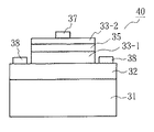
図4は、本発明の半導体発光素子のその他の例を示す構成図である。
【0044】
図4に示す半導体発光素子40は、基板31上において、下地層32、n型導電層33−1及び33−2、並びにこれらn型導電層で挟まれるようにしてp型導電層35を具えている。下地層32の表面は部分的に露出しており、この露出した表面部分に電極37が設けられているとともに、n型導電層33−1上においてn型電極38が形成され、いわゆるヘテロ接合バイポーラ型トランジスタ構成の半導体受光素子を構成している。
【0045】
n型導電層33−1及び33−2、並びにp型導電層35は窒化物半導体層群を構成しており、この窒化物半導体層群と、電極37及びn型電極38とから受光素子構造が構成される。
【0046】
下地層32は、上述したように、Alを50原子%以上含み、転位密度が1011/cm2以下の窒化物半導体から構成されていることが必要であり、さらには1010/cm2以下であることが好ましい。下地層22は、AlNから構成されていることが好ましい。
【0047】
また、Alを含む高結晶性の窒化物半導体からなる上記下地層32は、図2及び図3に示す半導体受光素子の場合と同様に、MOCVD法などによって、1100℃以上、好ましくは1250℃以下に加熱して基板32上に成膜することによって簡易に得ることができる。また、図2に示すPIN型の半導体受光素子20の場合と同様の理由から、下地層32の膜厚は0.5〜3μmであり、好ましくは1μm〜3μmとする。
【0048】
また、窒化物半導体層群を構成するn型導電層33−1及び33−2、並びにp型導電層35は、本発明にしたがって、下地層32を構成する窒化物半導体よりも少ない含有量でAlを含み、転位密度が1010/cm2以下の窒化物半導体から構成されていることが必要である。なお、図2及び図3に示す半導体受光素子の場合と同様に、下地層32とn型導電層33−1との間の組成差が大きくなることによって、n型導電層33−1中の転位密度が低減され、その結果、その上方に位置するp型導電層35及びn型導電層33−2中の転位密度も低減することができる。具体的には、109/cm2以下にまで転位密度を低減することができる。
【0049】
図4に示すヘテロ接合バイポーラ型トランジスタ構成の半導体受光素子40においては、カットオフ波長以下の波長の光が受光素子構造に入射することによってn型導電層33−1及び33−2、並びにp型導電層35が励起され、電極37及び38を介して、半導体受光素子40を含む所定の電気回路に電流が流れるようになる。したがって、この電流値を計測することによって入射した光の検出を行うことができる。
【0050】
なお、図4に示すように、p型導電層をn型導電層で挟むような構成とする代わりに、n型導電層をp型導電層で挟むような構成とすることもできる。
【0051】
また、図4に示すヘテロ接合バイポーラ型トランジスタ構成の半導体受光素子40においても、基板31は、上述したサファイア単結晶から構成する。サファイア単結晶は、図2に示すPIN型の半導体受光素子20の場合と同様の理由から、下地層32を形成するに先立って、表面窒化処理を施す。
【0052】
図5は、本発明の半導体発光素子のさらに他の例を示す構成図である。
【0053】
図5に示す半導体発光素子50は、基板41上において、下地層42、導電層43、及び半導体層44を具えている。導電層43の表面は部分的に露出しており、この露出した表面部分に電極47が設けられているとともに、半導体層44上において電極48が形成され、いわゆるヘテロ接合FET型トランジスタ構成の半導体受光素子を構成している。
【0054】
導電層43及び半導体層44は窒化物半導体層群を構成しており、この窒化物半導体層群と、電極47及48とから受光素子構造が構成される。
【0055】
下地層42は、上述したように、Alを50原子%以上含み、転位密度が1011/cm2以下の窒化物半導体から構成されていることが必要であり、さらには1010/cm2以下であることが好ましい。下地層22は、AlNから構成されていることが好ましい。
【0056】
また、Alを含む高結晶性の窒化物半導体からなる上記下地層42は、図2〜図4に示す半導体受光素子の場合と同様に、MOCVD法などによって、1100℃以上、好ましくは1250℃以下に加熱して基板42上に成膜することによって簡易に得ることができる。また、図2に示すPIN型の半導体受光素子20の場合と同様の理由から、下地層42の膜厚は0.5〜3μmであり、好ましくは1μm〜3μmとする。
【0057】
また、窒化物半導体層群を構成する導電層43及びキャリア層44は、本発明にしたがって、下地層42を構成する窒化物半導体よりも少ない含有量でAlを含み、転位密度が1010/cm2以下の窒化物半導体から構成されていることが必要である。なお、図2〜図4に示す半導体受光素子の場合と同様に、下地層42と導電層43との間の組成差が大きくなることによって、導電層43中の転位密度が低減され、その結果、その上方に位置するキャリア層44中の転位密度も低減することができる。具体的には、109/cm2以下にまで転位密度を低減することができる。
【0058】
図5に示すヘテロ接合FET型トランジスタ構成の半導体受光素子50においては、受光素子構造にカットオフ波長以下の波長の光が入射することによってキャリア層44が励起され、キャリア層44から導電層43中に所定量のキャリアが注入される。すると、この注入されたキャリアは、導電層43の、キャリア層44との界面近傍に形成されたキャリア易動性の表面層43Aを通って流れ、電極47及び48を介して、半導体受光素子50を含む所定の電気回路に電流が流れるようになる。したがって、この電流値を計測することによって入射した光の検出を行うことができる。
【0059】
また、図5に示すヘテロ接合FET型トランジスタ構成の半導体受光素子50においても、基板41は、上述したサファイア単結晶から構成する。サファイア単結晶は、図2に示すPIN型の半導体受光素子20の場合と同様の理由から、下地層42を形成するに先立って、表面窒化処理を施す。
【0060】
図2〜図4に示す半導体受光素子においては、基板がサファイア単結晶から構成され、下地層がAlNから構成され、導電層がGaを比較的多く含むAlGaNから構成されている場合においては、下地層中におけるAlの含有量を基板側から導電層側に向けて連続的又はステップ状に減少させることが好ましい。
【0061】
この場合、下地層中において、基板側のAl含有量は高く、導電層側のAl含有量は低くなるので、下地層の基板との格子定数差、並びに下地層の導電層との格子定数差が小さくなる。これによって、下地層を比較的厚く形成した場合においても、前記下地層内に発生する引張応力を補完して、下地層内におけるクラックの発生を抑制することができるようになる。
【0062】
また、高結晶性の窒化物半導体層から構成される本発明の半導体受光素子においては、その反り量が5cm当たり100μm以下にまで低減される。したがって、素子内における残留応力は極めて低くなり、上記半導体受光素子を長期間使用した場合においても、前記残留応力に起因した破損や特性変化を抑制することができる。
【0063】
【実施例】
本実施例においては、図2に示すPIN型の半導体受光素子を作製した。
【0064】
基板11として2インチ径の厚さ500μmのサファイア単結晶を用い、これをMOCVD装置の中に設置した。MOCVD装置には、ガス系としてH2、N2、TMA、TMG、Cp2Mg、NH3、SiH4が取り付けてある。圧力を15Torrに設定した後、H2を平均流速3m/secで流しながら、基板11を1150℃まで昇温した。
【0065】
そして、アンモニアガス(NH3)を水素キャリアガスとともに5分間流し、基板11の主面を窒化させた。なお、ESCAによる分析の結果、この表面窒化処理によって、前記主面には窒化層が形成されており、前記主面から深さ1nmにおける窒素含有量が7原子%であることが判明した。
【0066】
その後、TMAとNH3とを、供給ガスモル比が450対1となるようにして、下地層12としてのAlN層を厚さ1μmまで成長させた。この際、成膜速度を1μm/hrとなるように、TMA及びNH3の供給量を設定した。このAlN層中の転位密度をTEMによって観察したところ、8×109/cm2であった。
【0067】
次いで、基板温度を1120℃に設定した後、TMA、TMG、NH3、SiH4を全ガス平均流速3m/secで流して、n型導電層13としてSiをドープしたn−Al0.4Ga0.6N層を厚さ2μm成長させた。この際、NH3、TMA、及びTMGの平均供給ガスモル比は、600対2対8となるようにし、供給量は成膜速度が1.5μm/hrとなるように設定した。なお、SiH4は、キャリア濃度が3×1017/cm3となるように供給した。
【0068】
次いで、SiH4ガスの供給を停止し、前記n−Al0.4Ga0.6N層上に、受光層14としてのi−Al0.4Ga0.6N層を厚さ0.005μmに形成した。ここでTMAの供給を停止するとともに、Cp2Mgをキャリア濃度が3×10¹⁷/cm3となるようにして供給し、p型導電層15としてのMgをドープしたp−GaN層を厚さ0.5μmに形成した。
【0069】
n−Al0.4Ga0.6N層、i−Al0.4Ga0.6N層及びp−GaN層の転位密度をTEMによって観察したところ、それぞれ5×10⁸/cm2、5×108/cm2及び3×108/cm2であった。
【0070】
さらに、これらの各層を部分的にエッチング除去することによって、n型導電層13を構成するn−Al0.4Ga0.6N層の一部を露出させ、この露出部分に対してAl/Tiからなるn型電極17を形成した。また、p型導電層15を構成するp−GaN層上にAu/Niからなるp型電極18を形成した。
【0071】
このようにして作製した半導体受光素子20の暗電流を調べたところ、10pA/mm2であることが判明した。
【0072】
(比較例)
本比較例においては、図1に示すPIN型の半導体受光素子を作製した。
最初に、基板1としてのサファイア単結晶基板を実施例と同様の前処理を施した後、実施例と同様のMOCVD装置内に設置した。
【0073】
圧力を100Torrに設定した後、H2を平均ガス流速1.5m/secで流しながら、基板1の表面クリーニングを行うため、基板1を1100℃まで昇温した後、10分間保持し、その後600℃まで下げた。その後、TMGとNH3を供給ガスモル比が1500対1となるように供給して、バッファ層6としてのGaN層を厚さ0.03μmに形成した。
【0074】
その後、一旦、TMG及びNH3の供給を中断し、基板温度を1050℃に設定して、新たにバッファ層成膜時と同条件でTMG及びNH3を供給し、下地層2としてのi−GaN層を、成膜速度2μm/hrで厚さ3μmに形成した。このi−GaN層中の転位密度をTEM観察によって測定したところ、2×1010/cm2であることが判明した。
【0075】
次いで、実施例と同様にして、厚さ0.5μmのn−Al0.4Ga0.6N層、厚さ0.005μmのi−Al0.4Ga0.6N層、及び厚さ0.5μmのp−GaN層を、実施例と同様の条件で、それぞれn型導電層3、受光層4、及びp型導電層5として形成し、さらにAl/Tin型電極7、Au/Nip型電極8を形成することによって、半導体受光素子10を作製した。
【0076】
n型導電層3、受光層4、及びp型導電層5を構成するn−Al0.4Ga0.6N層、i−Al0.4Ga0.6N層、及びp−GaN層中における転位密度をTEM観察によって測定したところ、それぞれ8×10¹⁰/cm2、8×1010/cm2及び3×1010/cm2であった。
【0077】
このようにして作製した半導体受光素子10の暗電流を測定したところ、30pA/mm2であることが判明した。
【0078】
以上、実施例及び比較例から明らかなように、本発明に従って作製された半導体受光素子20は、下地層の高結晶性に起因して各層の結晶性も改善され、転位量が低減されているため、これによって暗電流が減少していることが分かる。したがって、実施例に示す半導体受光素子は、比較例に示す半導体受光素子と比較して、実際の光検出装置などとして用いた場合に、極めて良好な検出感度を呈することが分かる。
【0079】
以上、具体例を挙げながら、本発明を発明の実施の形態に即して詳細に説明してきたが、本発明は上記内容に限定されるものではなく、本発明の範疇を逸脱しない限りにおいてあらゆる変形や変更が可能である。例えば、導電層や受光層などの結晶性をさらに向上させる目的で、下地層と導電層との間などにバッファ層やひずみ超格子などの多層積層構造を温度、流量、圧力、原料供給量、及び添加ガスなどの成長条件を変化させることにより、挿入することもできる。
【0080】
また、上記下地層は、Ge、Si、Mg、Zn、Be、P、及びBなどの添加元素を含有することもできる。さらに、意識的に添加した元素に限らず、成膜条件などに依存して必然的に取り込まれる微量元素、並びに原料、反応管材質に含まれる微量不純物を含むこともできる。
【0081】
また、本発明の半導体受光素子は、上述したPIN型やMIS型などの半導体受光素子のみならず、あらゆる型の半導体受光素子に対して用いることができる。
【0082】
【発明の効果】
以上説明したように、本発明の半導体受光素子の製造方法は、特に、表面窒化処理を施したサファイア単結晶基板を1100℃以上に昇温し、転位密度が10 11 /cm 2 以下であり、Al含有量が50原子%以上である窒化物半導体からなる膜厚が0.5〜3μmの下地層を形成しているため、従来のようなバッファ層を必要とせずに、基板との格子定数差を補完して導電層や受光層などのエピタキシャル成長を可能とする。さらには、下地層の高結晶性に基づいて前記導電層や前記受光層などの結晶性を改善し、低転位化することができる。
【0083】
この結果、本発明の半導体受光素子は、低転位密度の窒化物半導体層群から構成される受光素子構造を有するようになるため、実際の使用において、暗電流を抑制して光検出感度を向上させることができる。
【図面の簡単な説明】
【図1】従来の半導体発光素子の一例を示す構成図である。
【図2】本発明の半導体発光素子の一例を示す構成図である。
【図3】本発明の半導体発光素子の他の例を示す構成図である。
【図4】本発明の半導体発光素子のその他の例を示す構成図である。
【図5】本発明の半導体発光素子のさらに他の例を示す構成図である。
【符号の説明】
1、11、21、31、41 基板、2、12、22、32、42 下地層、3、13、33−1、33−2 n型導電層、4、14、24 受光層、5、15、35 p型導電層、6 バッファ層、7、17、37 n型電極、8、18p型電極、10、20、30、40、50 半導体受光素子、23、43 導電層、27、28 ショットキー電極、38、47、48 電極、44 キャリア層[0001]
BACKGROUND OF THE INVENTION
The present invention relates to a semiconductor light receiving element.Manufacturing methodIn detail, a semiconductor light receiving element that can be suitably used as a photodiode or the likeManufacturing methodAbout.
[0002]
[Prior art]
In recent years, not only automatic controllers, optical measuring instruments, optical communications, but also daily goods such as televisions, videos, stereos, air conditioners, etc., have been incorporated semiconductor light-receiving elements such as photodiodes as photodetectors. . As such a semiconductor light-receiving element, a Ga-based nitride semiconductor has been used because it is a direct transition type and has a large inter-band gap, and the inter-band gap can be freely changed by composition control.
[0003]
FIG. 1 is a configuration diagram showing an example of a conventional so-called PIN type semiconductor light receiving element.
[0004]
In the semiconductor
[0005]
When light having a wavelength equal to or shorter than the cutoff wavelength to be detected is incident on the semiconductor
[0006]
[Problems to be solved by the invention]
In the semiconductor
[0007]
As a result, a relatively large amount of dislocations are contained in the buffer layer 6, and some of the dislocations are threading dislocations in the underlayer 2, the n-type
[0008]
When a semiconductor light-receiving element is formed from such a high dislocation and low crystalline layer, a so-called relatively large dark current flows through the dislocation of each layer. Therefore, when a current obtained by making light incident on the semiconductor light receiving element and exciting the light receiving layer is detected, an error in the detected current becomes large due to the dark current, and the S / N ratio or the detection is detected. There was a problem that the sensitivity deteriorated remarkably.
[0009]
An object of this invention is to provide the semiconductor light receiving element which reduces a dark current and has high detection sensitivity.
[0010]
[Means for Solving the Problems]
In order to achieve the above object, a method for manufacturing a light receiving element structure of the present invention is a method for manufacturing a light receiving element structure made of a nitride semiconductor on a sapphire single crystal substrate using MOCVD,A first step of performing surface nitriding treatment on the sapphire single crystal substrate and surface nitriding treatment were performed.Sapphire single crystal substrateTo 1100 ° C. or higher,Dislocation density is 1011/ Cm2Is,AlThe content is 50 atomic% or moreMade of nitride semiconductorThe film thickness is 0.5-3μmUnderlayerTheForming first2And the dislocation density on the underlayer is less than that of the underlayer and 1010/ Cm2Forming a nitride semiconductor layer group constituting a light receiving element structure containing Al with a smaller content than the nitride semiconductor constituting the underlying layer.3It has the process of this.
[0011]
The present inventors have intensively studied to achieve the above object. Since the dark current described above is generated as a result of high dislocation based on the low crystallinity of each layer constituting the semiconductor light receiving element, the present inventors reduced the amount of dislocation in each layer constituting the semiconductor light receiving element. Attempts were made to improve crystallinity.
[0012]
As described above, the dislocation in each layer constituting the semiconductor light receiving element is caused by the low crystalline buffer layer. However, in the conventional semiconductor light receiving element shown in FIG. 1, since a sapphire single crystal is used as the substrate 1 and GaN is used as the base layer 2, dislocation penetrates the conductive layer formed on the base layer. There was a problem that. In particular, when a conductive layer containing Al is formed, dislocations increase at the interface, and further cracks are generated. This is because tensile stress is generated in the conductive layer because the lattice constant is reduced when the conductive layer contains Al.
[0013]
Therefore, various studies were made not only on the buffer layer but also on the underlayer. In the conventional semiconductor light receiving element shown in FIG. 1, the conductive layer and the light receiving layer are both composed of a nitride semiconductor mainly containing Ga, as is apparent from the structure. Accordingly, it has been naturally considered that the underlayer for each of these layers is also composed of, for example, GaN mainly composed of Ga. As a result, lattice mismatch with the substrate occurs, and a low-temperature buffer layer is required to alleviate this.
[0014]
However, the present inventors paid attention to the composition of the underlayer, which was supposed to be natural, and tried to change this composition. As a result, the inventors have conceived that the underlayer is composed of a nitride semiconductor mainly composed of low crystalline dislocations and large crystalline Al. Even when the buffer layer is not present, the underlayer can be epitaxially grown on a substrate such as sapphire while complementing a large lattice constant difference. Further, based on the high crystallinity of the underlayer, the crystallinity of the conductive layer and the light receiving layer formed on the underlayer is also improved, and the amount of dislocations thereof is reduced.
[0015]
As a result, the dislocation amount is reduced in each layer constituting the semiconductor light receiving element, and generation of a high dark current based on the high dislocation amount can be effectively suppressed. For this reason, the error of the detection current value based on the dark current is reduced, and the detection sensitivity of the semiconductor light receiving element can be improved.
[0016]
DETAILED DESCRIPTION OF THE INVENTION
Hereinafter, the present invention will be described in detail according to embodiments of the invention.
FIG. 2 is a configuration diagram showing an example of the semiconductor light receiving element of the present invention.
A semiconductor
[0017]
In FIG. 2, an n-
[0018]
[0019]
Further, the n-
[0020]
This is because the ratio of threading dislocations is reduced due to the Al composition difference between the
[0021]
The above-described effect is that as the content of Al in the nitride semiconductor constituting the
[0022]
Thus, the crystallinity of the n-
[0023]
For example, in the case where the
[0024]
As a result, the amount of dislocations in the light-receiving layer 14 and the p-
[0025]
The
[0026]
In addition, from the viewpoint of improving crystallinity, it is preferable that the film thickness of the
[0027]
Such a low dislocation density and high crystalline n-
[0028]
The substrate 11 is made of sapphire single crystal, ZnO single crystal, LiAlO.2Single crystal, LiGaO2Single crystal, MgAl2O4Single crystal, oxide single crystal such as MgO single crystal, Si single crystal, group IV-IV single crystal such as SiC single crystal, GaAs single crystal, AlN single crystal, GaN single crystal, and AlGaN single crystal III-V single crystal, ZrB2It can be constructed from known substrate materials, such as boride single crystals such asIn the present invention, a sapphire single crystal substrate is used..
[0029]
In the present invention,Sapphire single
[0030]
If the sapphire single crystal substrate having the surface nitride layer formed in this way is used, the crystallinity of the
[0031]
In this case, the crystallinity can be kept sufficiently high even when the temperature at which the
[0032]
Furthermore, by forming the
[0033]
The surface nitride layer is relatively thin, for example, formed to be 1 nm or less, or relatively thick, for example, thick so that the nitrogen content at a depth of 1 nm from the main surface is 2 atom% or more. Is preferred.
[0034]
In the semiconductor light-receiving element of the present invention shown in FIG. 2, the lower conductive layer of the light-receiving layer 4 is n-type and the upper conductive layer is p-type. However, they can be formed by reversing them.
[0035]
FIG. 3 is a block diagram showing another example of the semiconductor light receiving element of the present invention.
[0036]
A semiconductor
[0037]
In FIG. 3, the
[0038]
As described above, the
[0039]
Further, the
[0040]
Further, according to the present invention, the
[0041]
In the MIS type semiconductor
[0042]
In the MIS type semiconductor
[0043]
FIG. 4 is a block diagram showing another example of the semiconductor light emitting device of the present invention.
[0044]
4 includes a
[0045]
The n-type conductive layers 33-1 and 33-2 and the p-
[0046]
As described above, the
[0047]
The
[0048]
In addition, the n-type conductive layers 33-1 and 33-2 and the p-
[0049]
In the semiconductor
[0050]
As shown in FIG. 4, instead of a configuration in which the p-type conductive layer is sandwiched between the n-type conductive layers, a configuration in which the n-type conductive layer is sandwiched between the p-type conductive layers may be employed.
[0051]
Also in the semiconductor
[0052]
FIG. 5 is a block diagram showing still another example of the semiconductor light emitting device of the present invention.
[0053]
A semiconductor
[0054]
The conductive layer 43 and the
[0055]
As described above, the
[0056]
In addition, the
[0057]
Further, according to the present invention, the conductive layer 43 and the
[0058]
In the semiconductor
[0059]
Also in the semiconductor
[0060]
2 to 4, when the substrate is made of sapphire single crystal, the base layer is made of AlN, and the conductive layer is made of AlGaN containing a relatively large amount of Ga, It is preferable to reduce the content of Al in the formation continuously or stepwise from the substrate side toward the conductive layer side.
[0061]
In this case, in the underlayer, the Al content on the substrate side is high and the Al content on the conductive layer side is low, so that the lattice constant difference between the underlayer and the substrate and the lattice constant difference between the underlayer and the conductive layer Becomes smaller. As a result, even when the underlayer is formed to be relatively thick, the tensile stress generated in the underlayer can be supplemented and the occurrence of cracks in the underlayer can be suppressed.
[0062]
Further, in the semiconductor light receiving element of the present invention constituted by a highly crystalline nitride semiconductor layer, the amount of warpage is reduced to 100 μm or less per 5 cm. Therefore, the residual stress in the element becomes extremely low, and even when the semiconductor light receiving element is used for a long period of time, damage and characteristic changes due to the residual stress can be suppressed.
[0063]
【Example】
In this example, the PIN type semiconductor light receiving element shown in FIG. 2 was produced.
[0064]
A sapphire single crystal having a diameter of 2 inches and a thickness of 500 μm was used as the substrate 11, and this was placed in an MOCVD apparatus. For MOCVD equipment, the gas system is H2, N2, TMA, TMG, Cp2Mg, NHThree, SiHFourIs attached. After setting the pressure to 15 Torr,2The substrate 11 was heated to 1150 ° C. while flowing at an average flow rate of 3 m / sec.
[0065]
And ammonia gas (NH3) With a hydrogen carrier gas for 5 minutes to nitride the main surface of the substrate 11. As a result of analysis by ESCA, it was found that a nitride layer was formed on the main surface by this surface nitriding treatment, and the nitrogen content at a depth of 1 nm from the main surface was 7 atomic%.
[0066]
Then TMA and NHThreeThe AlN layer as the
[0067]
Next, after setting the substrate temperature to 1120 ° C., TMA, TMG, NH3, SiH4N-Al doped with Si as the n-
[0068]
Next, SiH4The gas supply is stopped and the n-Al0.4Ga0.6On the N layer, i-Al as the light receiving layer 140.4Ga0.6The N layer was formed to a thickness of 0.005 μm. Here, the supply of TMA is stopped and Cp2
[0069]
n-Al0.4Ga0.6N layer, i-Al0.4Ga0.6When the dislocation densities of the N layer and the p-GaN layer were observed by TEM, 5 × 10 5 respectively.8/
[0070]
Further, by partially etching away each of these layers, n-Al constituting the n-
[0071]
When the dark current of the semiconductor light-receiving
[0072]
(Comparative example)
In this comparative example, the PIN type semiconductor light receiving element shown in FIG. 1 was produced.
First, a sapphire single crystal substrate as the substrate 1 was subjected to the same pretreatment as in the example, and then placed in the same MOCVD apparatus as in the example.
[0073]
After setting the pressure to 100 Torr,2In order to perform surface cleaning of the substrate 1 while flowing at an average gas flow rate of 1.5 m / sec, the substrate 1 was heated to 1100 ° C., held for 10 minutes, and then lowered to 600 ° C. Then TMG and NHThreeWas supplied so that the supply gas molar ratio was 1500 to 1, and a GaN layer as the buffer layer 6 was formed to a thickness of 0.03 μm.
[0074]
Then, once TMG and NH3Is interrupted, the substrate temperature is set to 1050 ° C., and TMG and NH are newly formed under the same conditions as when the buffer layer is formed3And an i-GaN layer as the underlayer 2 was formed to a thickness of 3 μm at a deposition rate of 2 μm / hr. When the dislocation density in the i-GaN layer was measured by TEM observation, 2 × 10¹⁰/ Cm2It turned out to be.
[0075]
Then, in the same manner as in the example, n-Al having a thickness of 0.5 μm0.4Ga0.6N-layer, i-Al with a thickness of 0.005 μm0.4Ga0.6An N layer and a p-GaN layer having a thickness of 0.5 μm are formed as an n-type
[0076]
n-Al constituting n-type
[0077]
When the dark current of the semiconductor light-receiving
[0078]
As described above, as is clear from the examples and comparative examples, the semiconductor light-receiving
[0079]
As mentioned above, the present invention has been described in detail according to the embodiments of the present invention with specific examples. However, the present invention is not limited to the above-described contents, and is not limited to the scope of the present invention. Variations and changes are possible. For example, for the purpose of further improving the crystallinity of the conductive layer and the light receiving layer, a multilayer laminated structure such as a buffer layer and a strained superlattice is formed between the base layer and the conductive layer, such as temperature, flow rate, pressure, raw material supply amount, Further, it can be inserted by changing the growth conditions such as the additive gas.
[0080]
The underlayer can also contain additive elements such as Ge, Si, Mg, Zn, Be, P, and B. Furthermore, it is possible to include not only elements added intentionally but also trace elements that are inevitably taken in depending on the film forming conditions and the like, as well as trace impurities contained in the raw materials and reaction tube materials.
[0081]
In addition, the semiconductor light receiving element of the present invention can be used not only for the semiconductor light receiving elements such as the PIN type and the MIS type described above but also for all types of semiconductor light receiving elements.
[0082]
【The invention's effect】
As described above, the semiconductor light receiving element of the present inventionManufacturing methodIsIn particular, the sapphire single crystal substrate subjected to surface nitriding treatment is heated to 1100 ° C. or higher, and the dislocation density is 10 11 / Cm 2 Since an underlayer having a film thickness of 0.5 to 3 μm made of a nitride semiconductor having an Al content of 50 atomic% or more is formed.Without the need for a buffer layer as in the prior art, the lattice constant difference from the substrate is complemented to enable epitaxial growth of a conductive layer, a light receiving layer, or the like. Furthermore, based on the high crystallinity of the base layer, the crystallinity of the conductive layer, the light-receiving layer, etc. can be improved and the dislocation can be reduced.
[0083]
As a result, the semiconductor light-receiving element of the present invention has a light-receiving element structure composed of a nitride semiconductor layer group having a low dislocation density. Therefore, in actual use, the dark current is suppressed and the light detection sensitivity is improved. Can be made.
[Brief description of the drawings]
FIG. 1 is a configuration diagram illustrating an example of a conventional semiconductor light emitting device.
FIG. 2 is a configuration diagram showing an example of a semiconductor light emitting device of the present invention.
FIG. 3 is a configuration diagram showing another example of the semiconductor light emitting device of the present invention.
FIG. 4 is a configuration diagram showing another example of the semiconductor light emitting device of the present invention.
FIG. 5 is a configuration diagram showing still another example of the semiconductor light emitting device of the present invention.
[Explanation of symbols]
1, 11, 21, 31, 41
Claims (8)
前記サファイア単結晶基板に表面窒化処理を施す第1の工程と、
表面窒化処理を施したサファイア単結晶基板を1100℃以上に昇温し、転位密度が1011/cm2以下であり、Al含有量が50原子%以上である窒化物半導体からなる膜厚が0.5〜3μmの下地層を形成する第2の工程と、
前記下地層上に、転位密度が下地層よりも少なくかつ1010/cm2以下であり、前記下地層を構成する窒化物半導体よりも少ない含有量でAlを含む受光素子構造を構成する窒化物半導体層群を形成する第3の工程と
を有することを特徴とする受光素子の製造方法。A method for manufacturing a light receiving element structure made of a nitride semiconductor on a sapphire single crystal substrate using MOCVD,
A first step of surface nitriding the sapphire single crystal substrate;
The sapphire single crystal substrate subjected to the surface nitriding treatment is heated to 1100 ° C. or higher, the dislocation density is 10 11 / cm 2 or lower, and the film thickness of the nitride semiconductor having an Al content of 50 atomic% or higher is 0. a second step of forming an underlying layer of .5~3Myuemu,
On the underlayer, the dislocation density is less than that of the underlayer and 10 10 / cm 2 or less, and the nitride constituting the light receiving element structure containing Al with a smaller content than the nitride semiconductor constituting the underlayer the manufacturing method of the light-receiving element and having a third step of forming a semiconductor layer group.
Priority Applications (3)
| Application Number | Priority Date | Filing Date | Title |
|---|---|---|---|
| JP2001266930A JP4209097B2 (en) | 2001-05-24 | 2001-09-04 | Semiconductor photo detector |
| US10/147,046 US6597023B2 (en) | 2001-05-24 | 2002-05-17 | Semiconductor light-detecting element |
| EP02011379.1A EP1263057B1 (en) | 2001-05-24 | 2002-05-23 | Nitride light-detector with a low dislocation density |
Applications Claiming Priority (3)
| Application Number | Priority Date | Filing Date | Title |
|---|---|---|---|
| JP2001-155134 | 2001-05-24 | ||
| JP2001155134 | 2001-05-24 | ||
| JP2001266930A JP4209097B2 (en) | 2001-05-24 | 2001-09-04 | Semiconductor photo detector |
Publications (2)
| Publication Number | Publication Date |
|---|---|
| JP2003046111A JP2003046111A (en) | 2003-02-14 |
| JP4209097B2 true JP4209097B2 (en) | 2009-01-14 |
Family
ID=26615623
Family Applications (1)
| Application Number | Title | Priority Date | Filing Date |
|---|---|---|---|
| JP2001266930A Expired - Lifetime JP4209097B2 (en) | 2001-05-24 | 2001-09-04 | Semiconductor photo detector |
Country Status (3)
| Country | Link |
|---|---|
| US (1) | US6597023B2 (en) |
| EP (1) | EP1263057B1 (en) |
| JP (1) | JP4209097B2 (en) |
Families Citing this family (11)
| Publication number | Priority date | Publication date | Assignee | Title |
|---|---|---|---|---|
| JP4327339B2 (en) * | 2000-07-28 | 2009-09-09 | 独立行政法人物質・材料研究機構 | Semiconductor layer forming substrate and semiconductor device using the same |
| JP3831322B2 (en) * | 2001-12-25 | 2006-10-11 | 日本碍子株式会社 | Group III nitride film manufacturing method, epitaxial growth substrate, group III nitride film, group III nitride element epitaxial substrate, and group III nitride element |
| FR2853141A1 (en) * | 2003-03-26 | 2004-10-01 | Kyocera Corp | Semiconductor device comprises monocrystalline diboride substrate, semiconductor stopper layer and nitride semiconductor layer, for light emitting and receiving and other electronic devices |
| JP2005136200A (en) * | 2003-10-30 | 2005-05-26 | Univ Nagoya | Nitride semiconductor crystalline layer, manufacturing method therefor, and substrate for manufacturing the same |
| US7951617B2 (en) * | 2005-10-06 | 2011-05-31 | Showa Denko K.K. | Group III nitride semiconductor stacked structure and production method thereof |
| US20090166674A1 (en) * | 2006-05-24 | 2009-07-02 | Meijo University | Ultraviolet light receiving element |
| US7498645B2 (en) * | 2006-10-04 | 2009-03-03 | Iii-N Technology, Inc. | Extreme ultraviolet (EUV) detectors based upon aluminum nitride (ALN) wide bandgap semiconductors |
| WO2011048809A1 (en) * | 2009-10-21 | 2011-04-28 | パナソニック株式会社 | Solar cell and method for manufacturing the same |
| ITUB20155862A1 (en) | 2015-11-24 | 2017-05-24 | St Microelectronics Srl | NORMALLY OFF TYPE TRANSISTOR WITH REDUCED RESISTANCE IN THE STATE ON AND RELATIVE MANUFACTURING METHOD |
| DE102017124596A1 (en) * | 2017-10-20 | 2019-04-25 | Osram Opto Semiconductors Gmbh | Optoelectronic semiconductor component and method for producing an optoelectronic semiconductor component |
| WO2019225112A1 (en) * | 2018-05-23 | 2019-11-28 | 株式会社Sumco | Group iii nitride semiconductor substrate and method of producing same |
Family Cites Families (6)
| Publication number | Priority date | Publication date | Assignee | Title |
|---|---|---|---|---|
| US5679152A (en) | 1994-01-27 | 1997-10-21 | Advanced Technology Materials, Inc. | Method of making a single crystals Ga*N article |
| US5670798A (en) | 1995-03-29 | 1997-09-23 | North Carolina State University | Integrated heterostructures of Group III-V nitride semiconductor materials including epitaxial ohmic contact non-nitride buffer layer and methods of fabricating same |
| US5741724A (en) | 1996-12-27 | 1998-04-21 | Motorola | Method of growing gallium nitride on a spinel substrate |
| US6104074A (en) * | 1997-12-11 | 2000-08-15 | Apa Optics, Inc. | Schottky barrier detectors for visible-blind ultraviolet detection |
| US6064078A (en) * | 1998-05-22 | 2000-05-16 | Xerox Corporation | Formation of group III-V nitride films on sapphire substrates with reduced dislocation densities |
| US6495894B2 (en) | 2000-05-22 | 2002-12-17 | Ngk Insulators, Ltd. | Photonic device, a substrate for fabricating a photonic device, a method for fabricating the photonic device and a method for manufacturing the photonic device-fabricating substrate |
-
2001
- 2001-09-04 JP JP2001266930A patent/JP4209097B2/en not_active Expired - Lifetime
-
2002
- 2002-05-17 US US10/147,046 patent/US6597023B2/en not_active Expired - Lifetime
- 2002-05-23 EP EP02011379.1A patent/EP1263057B1/en not_active Expired - Lifetime
Also Published As
| Publication number | Publication date |
|---|---|
| EP1263057B1 (en) | 2013-10-09 |
| EP1263057A1 (en) | 2002-12-04 |
| US20020175389A1 (en) | 2002-11-28 |
| JP2003046111A (en) | 2003-02-14 |
| US6597023B2 (en) | 2003-07-22 |
Similar Documents
| Publication | Publication Date | Title |
|---|---|---|
| US6524932B1 (en) | Method of fabricating group-III nitride-based semiconductor device | |
| US7199408B2 (en) | Semiconductor multilayer structure, semiconductor device and HEMT device | |
| US6630692B2 (en) | III-Nitride light emitting devices with low driving voltage | |
| US8486807B2 (en) | Realizing N-face III-nitride semiconductors by nitridation treatment | |
| CN105428482B (en) | A kind of LED epitaxial structure and production method | |
| US20180308940A1 (en) | Semiconductor wafer, semiconductor device, and method for manufacturing nitride semiconductor layer | |
| US9190268B2 (en) | Method for producing Ga-containing group III nitride semiconductor | |
| CN107195736B (en) | Gallium nitride-based light emitting diode epitaxial wafer and growth method thereof | |
| JPH06232451A (en) | Growing method of p-type gallium nitride | |
| US8536565B2 (en) | Nitride-based light-emitting device | |
| US20180047868A1 (en) | Iii-nitride led with tunnel junction | |
| JP4209097B2 (en) | Semiconductor photo detector | |
| JPH05283744A (en) | Semiconductor element | |
| US20150084163A1 (en) | Epitaxial substrate, semiconductor device, and method for manufacturing semiconductor device | |
| US8222639B2 (en) | Nitride based semiconductor device and method of manufacturing the same | |
| EP2525417A2 (en) | Nitride semiconductor device, nitride semiconductor wafer and method for manufacturing nitride semiconductor layer | |
| CN101289173B (en) | Method for preparing p-typed III-nitride material impured at superlattice positions | |
| US7135347B2 (en) | Method for manufacturing nitride film including high-resistivity GaN layer and epitaxial substrate manufactured by the method | |
| CN216450669U (en) | Epitaxial wafer and semiconductor light-emitting device | |
| WO1999059195A1 (en) | Crystal growth method for group-iii nitride and related compound semiconductors | |
| CN105870278A (en) | Gallium nitride based light emitting diode and preparation method therefor | |
| US20200144451A1 (en) | Nitride semiconductor crystal and method of fabricating the same | |
| US8562738B2 (en) | Nitride-based light-emitting device | |
| JP2002359390A (en) | Semiconductor light reception element | |
| Parish et al. | AlGaN/GaN solar-blind ultraviolet photodiodes on SiC substrate |
Legal Events
| Date | Code | Title | Description |
|---|---|---|---|
| A977 | Report on retrieval |
Free format text: JAPANESE INTERMEDIATE CODE: A971007 Effective date: 20060104 |
|
| A131 | Notification of reasons for refusal |
Free format text: JAPANESE INTERMEDIATE CODE: A131 Effective date: 20061003 |
|
| A521 | Request for written amendment filed |
Free format text: JAPANESE INTERMEDIATE CODE: A523 Effective date: 20061114 |
|
| A131 | Notification of reasons for refusal |
Free format text: JAPANESE INTERMEDIATE CODE: A131 Effective date: 20061219 |
|
| A521 | Request for written amendment filed |
Free format text: JAPANESE INTERMEDIATE CODE: A523 Effective date: 20070209 |
|
| RD03 | Notification of appointment of power of attorney |
Free format text: JAPANESE INTERMEDIATE CODE: A7423 Effective date: 20070209 |
|
| A02 | Decision of refusal |
Free format text: JAPANESE INTERMEDIATE CODE: A02 Effective date: 20070313 |
|
| A01 | Written decision to grant a patent or to grant a registration (utility model) |
Free format text: JAPANESE INTERMEDIATE CODE: A01 |
|
| A61 | First payment of annual fees (during grant procedure) |
Free format text: JAPANESE INTERMEDIATE CODE: A61 Effective date: 20081022 |
|
| R150 | Certificate of patent or registration of utility model |
Free format text: JAPANESE INTERMEDIATE CODE: R150 Ref document number: 4209097 Country of ref document: JP Free format text: JAPANESE INTERMEDIATE CODE: R150 |
|
| FPAY | Renewal fee payment (event date is renewal date of database) |
Free format text: PAYMENT UNTIL: 20111031 Year of fee payment: 3 |
|
| FPAY | Renewal fee payment (event date is renewal date of database) |
Free format text: PAYMENT UNTIL: 20121031 Year of fee payment: 4 |
|
| S201 | Request for registration of exclusive licence |
Free format text: JAPANESE INTERMEDIATE CODE: R314201 |
|
| FPAY | Renewal fee payment (event date is renewal date of database) |
Free format text: PAYMENT UNTIL: 20121031 Year of fee payment: 4 |
|
| R350 | Written notification of registration of transfer |
Free format text: JAPANESE INTERMEDIATE CODE: R350 |
|
| FPAY | Renewal fee payment (event date is renewal date of database) |
Free format text: PAYMENT UNTIL: 20121031 Year of fee payment: 4 |
|
| FPAY | Renewal fee payment (event date is renewal date of database) |
Free format text: PAYMENT UNTIL: 20131031 Year of fee payment: 5 |
|
| EXPY | Cancellation because of completion of term |