JP4208761B2 - Plasma display device - Google Patents
Plasma display device Download PDFInfo
- Publication number
- JP4208761B2 JP4208761B2 JP2004132809A JP2004132809A JP4208761B2 JP 4208761 B2 JP4208761 B2 JP 4208761B2 JP 2004132809 A JP2004132809 A JP 2004132809A JP 2004132809 A JP2004132809 A JP 2004132809A JP 4208761 B2 JP4208761 B2 JP 4208761B2
- Authority
- JP
- Japan
- Prior art keywords
- electrode
- display
- discharge
- display discharge
- discharge electrode
- Prior art date
- Legal status (The legal status is an assumption and is not a legal conclusion. Google has not performed a legal analysis and makes no representation as to the accuracy of the status listed.)
- Expired - Fee Related
Links
Images


Description
本発明は平面型テレビジョン及び情報表示ディスプレイ等に利用されるプラズマ表示装置に関し、特に高精細で明るい表示のAC面放電型のプラズマ表示装置に関する。 The present invention relates to a plasma display device used for a flat-screen television, an information display, and the like, and more particularly to a high-definition and bright display AC surface discharge plasma display device.
プラズマディスプレイはガス放電により発生した紫外線によって、蛍光体を励起発光させることにより表示を行う表示装置であり、大画面テレビ及び情報表示装置等への応用が期待されている。カラープラズマディスプレイには各種の方式が開発されているが、AC面放電型プラズマディスプレイが輝度及びパネル製造のしやすさ等の点で優れている。図18は代表的な反射型のAC面放電型カラープラズマディスプレイパネルの構造を示す模式図である。また、図19(a)は、同じく、従来のカラープラズマディスプレイパネルにおける面放電電極を構成する走査電極、維持電極及びバス電極の間の位置関係を示す模式図、(b)は隔壁とデータ電極との間の位置関係を示す模式図である。 A plasma display is a display device that performs display by exciting and emitting phosphors with ultraviolet rays generated by gas discharge, and is expected to be applied to large-screen televisions and information display devices. Various types of color plasma displays have been developed, but the AC surface discharge type plasma display is superior in terms of brightness and ease of panel manufacture. FIG. 18 is a schematic diagram showing the structure of a typical reflective AC surface discharge type color plasma display panel. FIG. 19A is a schematic diagram showing the positional relationship among scan electrodes, sustain electrodes, and bus electrodes that constitute surface discharge electrodes in a conventional color plasma display panel, and FIG. 19B shows barrier ribs and data electrodes. It is a schematic diagram which shows the positional relationship between these.
表示側基板となる前面基板100においては、ガラス基板1上に面放電電極として帯状の透明電極膜3及び幅の狭い帯状のバス電極4が多数本平行に形成されている。透明電極膜3としては、ITO薄膜又は酸化錫薄膜が使用可能であるが、大面積パネルの発光に十分な放電電流を流すには、これらの薄膜の電気抵抗は大きい。このため、高い導電性を有する金属製のバス電極4が設けられている。このようなバス電極4としては、例えば厚膜銀又は銅、アルミニウム若しくはクロム等の金属薄膜からなる電極が使用されている。バス電極4上に誘電体層7が形成されている。一般的に、誘電体層7は、以下のようにして形成される。先ず、低融点ガラスペーストをバス電極4が形成された透明電極膜3上に塗布し、これを高温で焼成することにより、厚さが20乃至40μm程度の透明で絶縁耐圧が高いガラス層を形成する。その後、ガラス層の上に表面保護層として2次電子放出係数が大きく、且つ、耐スパッタ性にも優れた酸化マグネシウム薄膜を形成する。
In a
一方、前面基板100と平行に配設される背面基板200においては、ガラス基板2上に、帯状の複数本のデータ電極5及びこれらのデータ電極5を覆う誘電体層10が形成されている。誘電体層10は低融点ガラスを主成分としている。誘電体層10上に垂直方向(列方向)に延びる帯状の隔壁6が形成されている。隔壁6は、その幅が30乃至120μm程度、その高さは80乃至150μm程度の構造物であり、一般にアルミナ等の酸化物粉末と低融点ガラスとの混合物から構成されている。隔壁6により区画された複数本の溝の底部及び側面に粉末の蛍光体からなり赤色、緑色又は青色に発光する蛍光体層9が塗布されている。蛍光体層9の発光色は上述の順で水平方向(行方向)に並んでいる。
On the other hand, in the
そして、背面基板200と前面基板100とが組み合わされ、両基板の周囲がフリットガラスで封着され、加熱排気された後に希ガスを主成分とする放電ガスが封入されている。このようにして、カラープラズマディスプレイパネルが構成されている。
The
なお、隔壁6により、放電空間が確保されると共に、放電時のクロストーク及び発光色のにじみが防止されている。
The
前面基板100では、面放電電極が面放電ギャップ11を挟んで対になっている。即ち、一方が面放電電極(走査電極)13、他方が面放電電極(維持電極)14となっている。そして、従来のカラープラズマディスプレイパネルにおいては、これらの電極13及び14に背面基板200に設けられたデータ電極5を加えた3種類の電極に各種の電圧波形を印加することにより駆動表示される。
In the
図22は第n行目の走査電極をSn、維持電極をCnとして、各電極に印加される駆動波形を示すタイミングチャートである。 FIG. 22 is a timing chart showing drive waveforms applied to the respective electrodes with Sn as the scan electrode in the nth row and Cn as the sustain electrode.
走査電極Sn、Sn+1、Sn+2、Sn+3、…には、走査パルスが順次印加される。このタイミングに合わせて、データ電極Djに当該走査電極上の表示セルの表示データに応じて、走査パルスとは逆極性のデータパルスが印加される。これにより、走査電極Sn、…とデータ電極Djとの間に対向放電が発生する。この対向放電による書込み動作により、走査電極Sn、…の表面に正電荷の壁電荷が生成される。壁電荷が生成された表示セルでは、その後に維持電極Cmと走査電極Sn、…との間に印加される維持パルスにより面放電が発生する。 Scan pulses are sequentially applied to the scan electrodes Sn, Sn + 1, Sn + 2, Sn + 3,. In synchronization with this timing, a data pulse having a polarity opposite to that of the scan pulse is applied to the data electrode Dj in accordance with the display data of the display cell on the scan electrode. As a result, a counter discharge is generated between the scan electrodes Sn,... And the data electrode Dj. By the address operation by this counter discharge, positive wall charges are generated on the surface of the scan electrodes Sn,. In the display cell in which the wall charges are generated, surface discharge is generated by the sustain pulse applied between the sustain electrode Cm and the scan electrodes Sn,.
一方、データパルスが印加されず、データ電極と走査電極との間で放電が発生しなかったため、壁電荷が生成されずに書込みがなされなかった表示セルでは、壁電荷による電場の重畳効果がないため、維持パルスが印加されても維持放電は発生しない。 On the other hand, since no data pulse is applied and no discharge is generated between the data electrode and the scan electrode, there is no effect of superposition of the electric field due to the wall charge in the display cell in which the wall charge is not generated and writing is not performed. Therefore, no sustain discharge occurs even when a sustain pulse is applied.
そして、壁電荷が生成された表示セルに維持パルスを所定の回数印加することにより、発光表示が行われる。 Then, a sustaining pulse is applied a predetermined number of times to the display cell where the wall charges are generated, thereby performing light emission display.
なお、維持電極Cmには走査パルスのように1本ごとに選択されるパルスを印加する必要がないため、各維持電極Cmは共通接続され、図22に示すように、同じ電圧波形が印加されている。また、実用パネルでは書込み動作性向上のために、書込み動作に先だって全てのセルに高電圧が印加され、強制的に放電が行われる予備放電動作等により、セル内の活性化及び適当な壁電荷生成を目的とした準備シーケンスが採用されている。 Since it is not necessary to apply a pulse selected for each sustain electrode to the sustain electrode Cm, each sustain electrode Cm is connected in common, and the same voltage waveform is applied as shown in FIG. ing. In practical panels, in order to improve the write operability, activation in the cells and appropriate wall charges are performed by a pre-discharge operation in which a high voltage is applied to all cells prior to the write operation and the discharge is forced. A preparation sequence for the purpose of generation is employed.
AC型プラズマディスプレイの階調表示には、サブフィールド法が採用されている。これは、AC型プラズマディスプレイでは、発光表示輝度の電圧変調は困難であり、輝度変調には発光回数を変える必要があるためである。サブフィールド法は多階調画像を複数の2値表示画像に分解し、高速で連続表示することにより、視覚の積分効果により多階調画像を再現するものである。 The subfield method is adopted for gradation display of the AC plasma display. This is because voltage modulation of light emission display luminance is difficult in the AC type plasma display, and it is necessary to change the number of times of light emission for luminance modulation. In the subfield method, a multi-gradation image is decomposed into a plurality of binary display images and continuously displayed at a high speed to reproduce the multi-gradation image by visual integration effect.
しかしながら、このような従来の面放電型ACプラズマディスプレイは優れた特性を有しているものの、図18に示した面放電電極の構造から分かるように、1表示行の発光に対を構成する2本の面放電電極が必要である。このような面放電電極における面放電ギャップは50乃至100μm程度と比較的狭いが、垂直方向で隣接する表示行間に設けられる非放電のギャップは、放電のクロストークを避けるために、面放電ギャップの3倍程度以上の幅が必要とされている。また、金属製のバス電極4には、材料の比抵抗及び大面積パネルの製造技術の限界から100μm程度の幅が必要とされている。このような制限のため、画素ピッチが狭くなって解像度が高くなるにつれて、面放電電極の面積及び開口率が小さくなり、高輝度を実現することが困難となるという問題点がある。
However, although such a conventional surface discharge AC plasma display has excellent characteristics, as can be seen from the structure of the surface discharge electrode shown in FIG. A surface discharge electrode is required. The surface discharge gap in such a surface discharge electrode is relatively narrow, about 50 to 100 μm. However, the non-discharge gap provided between the adjacent display rows in the vertical direction is a surface discharge gap in order to avoid discharge crosstalk. A width of about three times or more is required. Further, the
また、高解像度化に伴い走査本数が多くなるため、1行当たりの書込みに要する走査時間を短くする必要がある。通常のテレビジョン及び480行のVGAクラスでは、サブフィールド法によるフルカラー表示は可能であるが、1000行程度の走査本数となるHDTV(高密度テレビジョン)及び高解像度ディスプレイでは、走査時間が極めて短くなるため、確実な動作が困難となり、書込み不良及び誤点灯が発生して良好な表示ができなくなることも大きな課題となっている。 Further, since the number of scans increases as the resolution is increased, it is necessary to shorten the scan time required for writing per row. In a normal television and a 480-line VGA class, full-color display by the subfield method is possible. However, in an HDTV (high-density television) and a high-resolution display having about 1000 lines, the scanning time is extremely short. Therefore, it is difficult to perform reliable operation, and writing failure and erroneous lighting occur to prevent a good display from occurring.
そこで、面放電電極の面積及び開口率の改善を目的として、水平方向に延びる隔壁を設けその上にバス電極を設けたカラープラズマディスプレイパネルが提案されている。以下、このようなカラープラズマディスプレイパネルを第2の従来例といい、前述の従来のカラープラズマディスプレイパネルを第1の従来例という。図20(a)は面放電電極を構成する走査電極、維持電極及びバス電極の間の第2の従来例における位置関係を示す模式図、(b)は隔壁とデータ電極との間の第2の従来例における位置関係を示す模式図である。 Therefore, for the purpose of improving the area of the surface discharge electrode and the aperture ratio, a color plasma display panel has been proposed in which a partition wall extending in the horizontal direction is provided and a bus electrode is provided thereon. Hereinafter, such a color plasma display panel is referred to as a second conventional example, and the above-described conventional color plasma display panel is referred to as a first conventional example. FIG. 20A is a schematic diagram showing the positional relationship in the second conventional example among the scan electrode, sustain electrode, and bus electrode constituting the surface discharge electrode, and FIG. 20B is the second diagram between the barrier rib and the data electrode. It is a schematic diagram which shows the positional relationship in the prior art example.
第2の従来例においては、図20(a)に示すように、前面基板に設けられた面放電電極が水平方向に延びる幅広の透明電極15及びこの透明電極15の中央部に配置されたバス電極16から構成されている。また、図20(b)に示すように、隔壁17は、水平方向に延びる水平隔壁17a及びこの水平隔壁17aに区画された溝を更に複数個の表示セルに区画する垂直隔壁17bから構成されている。但し、隣接する1表示行間において、垂直隔壁17bの位置は表示セルの半分ずつずれている。即ち、隣接する1表示行間において、表示セルは三角配列となっている。そして、バス電極16が平面視で水平隔壁17aと重なるように組み立てられている。
In the second conventional example, as shown in FIG. 20A, the surface discharge electrode provided on the front substrate has a wide
このように構成された第2の従来例においては、1個の面放電電極が上下に隣接する2行に跨るいわゆる両側面放電電極構造となっており、図19(a)に示した第1の従来例と比較すると、バス電極による遮光及び非放電ギャップがない。従って、有効な面放電電極の面積及び開口率が大きくなっている。 In the second conventional example configured as described above, a single surface discharge electrode has a so-called double-sided surface discharge electrode structure extending over two adjacent rows, and the first surface discharge electrode shown in FIG. Compared with the conventional example, there is no light shielding and non-discharge gap by the bus electrode. Therefore, the effective area and aperture ratio of the surface discharge electrode are increased.
また、図20(b)に示すように、データ電極18が1個毎に交互に表示セルの間を縫っているので、両側面放電電極構造であるにも拘わらず、図22と同様の波形の駆動によっても、各表示セルを独立に選択し、書込みを行うことができる。
Further, as shown in FIG. 20 (b), since the
しかし、表示セルを三角配列とした場合、第1の従来例のようなストライプ配列と比して、混色がやや悪いこと及び文字表示の鮮鋭感がやや劣る等の問題点がある。また、第2の従来例においても、行数を、例えば480行とすると、480本の走査電極と480+1本の維持電極が必要となり、HDTV等の高精細高解像度プラズマディスプレイパネルの実現には困難が伴う。更に、放電のクロストークを防止するために表示セルが隔壁17a及び17bにより完全に仕切られているため、製造工程における排気コンダクタンスが極めて小さい。このため、排気処理に長時間を要したり、残留不純物によるパネル特性の悪化が生じやすい。特に、大面積かつ高精細のパネルにおいてこの問題点はより深刻になる。
However, when the display cells are arranged in a triangular pattern, there are problems such as slightly mixed colors and slightly inferior sharpness of character display as compared with the stripe array as in the first conventional example. In the second conventional example, if the number of rows is 480, for example, 480 scan electrodes and 480 + 1 sustain electrodes are required, which is difficult to realize a high-definition high-resolution plasma display panel such as an HDTV. Is accompanied. Further, since the display cell is completely partitioned by the
また、駆動方法に変更を加えることにより構造を簡素化したカラープラズマディスプレイパネルが提案されている(例えば、特許文献1(特開平11−65518号公報)参照。)。以下、この従来のカラープラズマディスプレイパネルを第3の従来例という。図21(a)は面放電電極を構成する走査電極、維持電極及びバス電極の間の第3の従来例における位置関係を示す模式図、(b)は隔壁とデータ電極との間の第3の従来例における位置関係を示す模式図である。 A color plasma display panel having a simplified structure by changing the driving method has been proposed (see, for example, Patent Document 1 (Japanese Patent Laid-Open No. 11-65518)). Hereinafter, this conventional color plasma display panel is referred to as a third conventional example. FIG. 21A is a schematic diagram showing the positional relationship in the third conventional example among the scan electrode, the sustain electrode, and the bus electrode constituting the surface discharge electrode, and FIG. 21B is a third diagram between the barrier rib and the data electrode. It is a schematic diagram which shows the positional relationship in the prior art example.
第3の従来例においては、第2の従来例において維持電極Cn、…を構成する透明電極及びバス電極が除かれて、走査電極Sn、Sn+1、Sn+2、Sn+3、…を構成する透明電極19の垂直方向の寸法が大きくなっている。また、隔壁22は井桁状となっており、この隔壁22により区画された表示セルの配列は、ストライプ配列である。
In the third conventional example, the transparent electrodes and bus electrodes constituting the sustain electrodes Cn,... In the second conventional example are removed, and the
このように構成された第3の従来例においては、行数を、例えば480行とすると、必要な面放電電極の数は、480+1個である。また、図21(a)及び(b)からも容易に分かるように、単位表示面積当たりの発光輝度に直接関係する面放電電極の面積を第1及び第2の従来例のものよりも広くとることができる。このように、面放電電極の個数を少なくし、面放電電極の面積を広くとることができるので、特に走査線数が多い高解像度かつ高精細のプラズマディスプレイパネルにおいて、第3の従来例は極めて有効である。 In the third conventional example configured as described above, if the number of rows is 480, for example, the number of necessary surface discharge electrodes is 480 + 1. Further, as can be easily understood from FIGS. 21A and 21B, the area of the surface discharge electrode that is directly related to the light emission luminance per unit display area is larger than that of the first and second conventional examples. be able to. Thus, since the number of surface discharge electrodes can be reduced and the area of the surface discharge electrodes can be increased, the third conventional example is extremely important in a high-resolution and high-definition plasma display panel having a large number of scanning lines. It is valid.
しかしながら、第3の従来例は、所期の目的を達成することはできたものの、特殊なインターレース駆動法で動作させる必要があり、動作マージンが狭いという問題点がある。また、図20(b)に示す第2の従来例と同様に、各表示セルが隔壁22で仕切られているため、製造工程における排気に極めて長時間を要し、パネル特性の面内均一性を得にくいという問題点もある。このため、実用化が困難である。
However, although the third conventional example can achieve the intended purpose, it needs to be operated by a special interlace driving method and has a problem that the operation margin is narrow. Further, as in the second conventional example shown in FIG. 20B, since each display cell is partitioned by the
本発明はかかる問題点に鑑みてなされたものであって、大きい面放電電極の面積及び開口率を得ることにより高解像度かつ高精細の表示を行うことができると共に、広い動作マージンを確保することができるプラズマ表示装置を提供することを目的とする。 The present invention has been made in view of such problems, and by obtaining a large surface discharge electrode area and aperture ratio, it is possible to perform high-resolution and high-definition display and ensure a wide operating margin. An object of the present invention is to provide a plasma display device capable of performing
本発明に係る第1のプラズマ表示装置は、行方向に延び相互に独立して駆動される複数のバス電極と、前記バス電極から見て第1の列方向に隣接するセル内に延出する第1の表示放電電極と、前記バス電極から見て前記第1の列方向と反対の第2の列方向に隣接するセル内に延出する第2の表示放電電極と、列方向に延びるデータ電極と、を有し、夫々行方向で隣接する表示セル間において前記第1の表示放電電極及び第2の表示放電電極は分離され、前記第1の表示放電電極の行方向の幅が前記第2の表示放電電極の行方向の幅より広いことにより、又は前記第1の表示放電電極の前記第1の方向の先端部における行方向の幅が前記第2の表示放電電極の前記第2の方向の先端部における行方向の幅より広いことにより、又は前記第1の表示放電電極の前記第1の方向の先端部の断面積が前記第2の表示放電電極の前記第2の方向の先端部の断面積より広いことにより、前記第1の表示放電電極と前記データ電極との間の放電開始電圧が前記第2の表示放電電極と前記データ電極との間の放電開始電圧より小さいものとされたことを特徴とする。 A first plasma display device according to the present invention extends to a plurality of bus electrodes extending in a row direction and driven independently from each other, and cells adjacent to each other in a first column direction as viewed from the bus electrodes. A first display discharge electrode; a second display discharge electrode extending into a cell adjacent to the second column direction opposite to the first column direction when viewed from the bus electrode; and data extending in the column direction And the first display discharge electrode and the second display discharge electrode are separated between display cells adjacent in the row direction, and the width of the first display discharge electrode in the row direction is the first display discharge electrode. The width of the second display discharge electrode in the row direction, or the width of the first display discharge electrode in the first direction in the row direction is the second of the second display discharge electrode. The first table by being wider than the width in the row direction at the tip of the direction; By cross-sectional area of the distal end portion of the first direction of the discharge electrodes is wider than the cross-sectional area of the distal end portion of the second direction of the second display discharge electrodes, the data electrode and the first display discharge electrodes The discharge start voltage between the second display discharge electrode and the data electrode is smaller than the discharge start voltage between the second display discharge electrode and the data electrode.
本発明に係る第2のプラズマ表示装置は、行方向に延び相互に独立して駆動される複数のバス電極と、前記バス電極から見て第1の列方向に隣接するセル内に延出する第1の表示放電電極と、前記バス電極から見て前記第1の列方向と反対の第2の列方向に隣接するセル内に延出する第2の表示放電電極と、列方向に延びるデータ電極と、を有し、前記第1の表示放電電極上に、電気伝導性を備えた突起部分が形成されていることにより、又は前記第1の表示放電電極上に形成された誘電体膜の厚さが、前記第2の表示放電電極上に形成された誘電体膜の厚さよりも薄いことにより、前記第1の表示放電電極と前記データ電極との間の放電開始電圧が前記第2の表示放電電極と前記データ電極との間の放電開始電圧より小さいものとされたことを特徴とする。 The second plasma display device according to the present invention extends in a cell adjacent to the plurality of bus electrodes extending in the row direction and driven independently from each other and in the first column direction as viewed from the bus electrodes. A first display discharge electrode; a second display discharge electrode extending into a cell adjacent to the second column direction opposite to the first column direction when viewed from the bus electrode; and data extending in the column direction And a dielectric film formed on the first display discharge electrode by forming a projecting portion having electrical conductivity on the first display discharge electrode. Since the thickness is smaller than the thickness of the dielectric film formed on the second display discharge electrode, the discharge start voltage between the first display discharge electrode and the data electrode is changed to the second display discharge electrode. this, which is a discharge starting voltage smaller ones between the data electrodes and the display discharge electrodes The features.
本発明に係る第3のプラズマ表示装置は、行方向に延び相互に独立して駆動される複数のバス電極と、前記バス電極から見て第1の列方向に隣接するセル内に延出する第1の表示放電電極と、前記バス電極から見て前記第1の列方向と反対の第2の列方向に隣接するセル内に延出する第2の表示放電電極と、列方向に延びるデータ電極と、を有し、前記第1の表示放電電極に対向する部分の前記データ電極の行方向の幅が前記第2の表示放電電極に対向する部分の前記データ電極の行方向の幅より狭いことにより、前記第1の表示放電電極と前記データ電極との間の放電開始電圧が前記第2の表示放電電極と前記データ電極との間の放電開始電圧より小さいものとされたことを特徴とする。 A third plasma display device according to the present invention includes a plurality of bus electrodes extending in the row direction and driven independently of each other, and extending into cells adjacent in the first column direction as viewed from the bus electrodes. A first display discharge electrode; a second display discharge electrode extending into a cell adjacent to the second column direction opposite to the first column direction when viewed from the bus electrode; and data extending in the column direction And the width in the row direction of the data electrode at the portion facing the first display discharge electrode is narrower than the width in the row direction at the portion facing the second display discharge electrode. Thus, the discharge start voltage between the first display discharge electrode and the data electrode is made smaller than the discharge start voltage between the second display discharge electrode and the data electrode. To do.
本発明に係る第4のプラズマ表示装置は、行方向に延び相互に独立して駆動される複数のバス電極と、前記バス電極から見て第1の列方向に隣接するセル内に延出する第1の表示放電電極と、前記バス電極から見て前記第1の列方向と反対の第2の列方向に隣接するセル内に延出する第2の表示放電電極と、列方向に延びるデータ電極と、を有し、前記データ電極の前記第2の表示放電電極に対向する部分は、前記セルの中心から行方向にずれて配置され、前記データ電極の前記第1の表示放電電極に対向する部分は、前記セルの中心と重なるように配置されていることにより、又は前記データ電極の前記第1の表示放電電極に対向する部分と前記第1の表示放電電極との間の距離が、前記データ電極の前記第2の表示放電電極に対向する部分と前記第2の表示放電電極との間の距離より短いことにより、前記第1の表示放電電極と前記データ電極との間の放電開始電圧が前記第2の表示放電電極と前記データ電極との間の放電開始電圧より小さいものとされたことを特徴とする。 The fourth plasma display device according to the present invention extends in a cell adjacent to each other in the first column direction when viewed from the bus electrodes, and a plurality of bus electrodes extending in the row direction and driven independently of each other. A first display discharge electrode; a second display discharge electrode extending into a cell adjacent to the second column direction opposite to the first column direction when viewed from the bus electrode; and data extending in the column direction And a portion of the data electrode facing the second display discharge electrode is arranged in a row direction away from the center of the cell and faces the first display discharge electrode of the data electrode The portion to be arranged so as to overlap the center of the cell, or the distance between the portion of the data electrode facing the first display discharge electrode and the first display discharge electrode is A portion of the data electrode facing the second display discharge electrode And by less than the distance between said second display discharge electrodes, and said data electrode discharge starting voltage and the second display discharge electrodes between the data electrode and the first display discharge electrodes It is characterized by being smaller than the discharge start voltage between.
本発明に係る第5のプラズマ表示装置は、行方向に延び相互に独立して駆動される複数のバス電極と、前記バス電極から見て第1の列方向に隣接するセル内に延出する第1の表示放電電極と、前記バス電極から見て前記第1の列方向と反対の第2の列方向に隣接するセル内に延出する第2の表示放電電極と、列方向に延びるデータ電極と、を有し、前記第1の表示放電電極の一部分と前記データ電極の前記第1の表示放電電極の一部分に対向する部分との間に存在する誘電体層の厚さは、前記第2の表示放電電極の一部分と前記データ電極の前記第2の表示放電電極の一部分に対向する部分との間に存在する誘電体層の厚さより薄くすることにより、又は前記第1の表示放電電極の一部分と前記データ電極の前記第1の表示放電電極の一部分に対向する部分との間に存在する誘電体層の誘電率は、前記第2の表示放電電極の一部分と前記データ電極の前記第2の表示放電電極の一部分に対向する部分との間に存在する誘電体層の誘電率より大きくすることにより、前記第1の表示放電電極と前記データ電極との間の放電開始電圧が前記第2の表示放電電極と前記データ電極との間の放電開始電圧より小さいものとされたことを特徴とする。
本発明に係る第6のプラズマ表示装置は、行方向に延び相互に独立して駆動される複数のバス電極と、前記バス電極から見て第1の列方向に隣接するセル内に延出する第1の表示放電電極と、前記バス電極から見て前記第1の列方向と反対の第2の列方向に隣接するセル内に延出する第2の表示放電電極と、列方向に延びるデータ電極と、を有し、前記第1の表示放電電極を覆う誘電体層の表面の2次電子放出係数が前記第2の表示放電電極を覆う誘電体層の表面の2次電子放出係数より大きいことにより、前記第1の表示放電電極と前記データ電極との間の放電開始電圧が前記第2の表示放電電極と前記データ電極との間の放電開始電圧より小さいものとされたことを特徴とする。
本発明に係る第7のプラズマ表示装置は、対向して配置された第1及び第2の基板と、前記第1の基板上に配置され行方向に延び相互に独立して駆動される複数のバス電極と、前記バス電極から見て第1の列方向に隣接するセル内に延出する第1の表示放電電極と、前記バス電極から見て前記第1の列方向と反対の第2の列方向に隣接するセル内に延出する第2の表示放電電極と、前記第2の基板上に配置され列方向に延びるデータ電極と、を有し、夫々行方向で隣接する表示セル間において前記第1の表示放電電極及び第2の表示放電電極は分離され、前記第1の表示放電電極の行方向の幅が前記第2の表示放電電極の行方向の幅より広いことにより、又は前記第1の表示放電電極の前記第1の方向の先端部における行方向の幅が前記第2の表示放電電極の前記第2の方向の先端部における行方向の幅より広いことにより、又は前記第1の表示放電電極の前記第1の方向の先端部の断面積が前記第2の表示放電電極の前記第2の方向の先端部の断面積より広いことにより、前記第1の表示放電電極と前記データ電極との間の放電開始電圧が前記第2の表示放電電極と前記データ電極との間の放電開始電圧より小さいものとされたことを特徴とする。
A fifth plasma display device according to the present invention includes a plurality of bus electrodes extending in the row direction and driven independently from each other, and extending into cells adjacent in the first column direction as viewed from the bus electrodes. A first display discharge electrode; a second display discharge electrode extending into a cell adjacent to the second column direction opposite to the first column direction when viewed from the bus electrode; and data extending in the column direction A dielectric layer existing between a portion of the first display discharge electrode and a portion of the data electrode facing a portion of the first display discharge electrode. by thinner than the thickness of the dielectric layer present between the portion and the portion facing the portion of the second display discharge electrodes of the data electrodes of the second display discharge electrodes, or the first display discharge A portion of the electrode and a portion of the first display discharge electrode of the data electrode The dielectric constant of the dielectric layer existing between the opposing portions exists between a portion of the second display discharge electrode and a portion of the data electrode facing a portion of the second display discharge electrode. By making the dielectric constant greater than the dielectric constant of the dielectric layer, the discharge start voltage between the first display discharge electrode and the data electrode is greater than the discharge start voltage between the second display discharge electrode and the data electrode. It is characterized by being made small.
A sixth plasma display device according to the present invention includes a plurality of bus electrodes extending in the row direction and driven independently from each other, and extending into cells adjacent in the first column direction when viewed from the bus electrodes. A first display discharge electrode; a second display discharge electrode extending into a cell adjacent to the second column direction opposite to the first column direction when viewed from the bus electrode; and data extending in the column direction a and the electrode, the two larger electron emission coefficient of the first display secondary electron emission coefficient covering said second display discharge electrodes dielectric layer surface of the surface of the discharge electrode covering the dielectric layer Thus, the discharge start voltage between the first display discharge electrode and the data electrode is made smaller than the discharge start voltage between the second display discharge electrode and the data electrode. To do.
A seventh plasma display device according to the present invention includes a plurality of first and second substrates disposed opposite to each other, and a plurality of substrates disposed on the first substrate and extending in a row direction and independently driven. A bus electrode; a first display discharge electrode extending into a cell adjacent in the first column direction as viewed from the bus electrode; and a second electrode opposite to the first column direction as viewed from the bus electrode A second display discharge electrode extending in a cell adjacent in the column direction; and a data electrode disposed on the second substrate and extending in the column direction, each between adjacent display cells in the row direction. The first display discharge electrode and the second display discharge electrode are separated, and the width of the first display discharge electrode in the row direction is wider than the width of the second display discharge electrode in the row direction, or The width in the row direction at the tip of the first display discharge electrode in the first direction is the second width. When the display discharge electrode is wider than the width in the row direction at the tip portion in the second direction, or the sectional area of the tip portion in the first direction of the first display discharge electrode is the second display discharge electrode. The discharge start voltage between the first display discharge electrode and the data electrode is between the second display discharge electrode and the data electrode. It is characterized by being smaller than the discharge start voltage.
また、前記複数のバス電極は、2本おきに前記走査パルスが印加される第1のグループ、前記第1の電圧が印加される第2のグループ及び前記第2の電圧が印加される第3のグループに分けられていてもよく、3本以上おきに前記走査パルスが印加される第1のグループ、前記第1の電圧が印加される第2のグループ、前記第2の電圧が印加される第3のグループ及びこれらの第1乃至第3のグループに属するバス電極を含まない1又は2以上のグループに分けられていてもよい。 The plurality of bus electrodes may include a first group to which the scan pulse is applied every second, a second group to which the first voltage is applied, and a third group to which the second voltage is applied. The first group to which the scan pulse is applied every three or more, the second group to which the first voltage is applied, and the second voltage are applied. You may divide into the 3rd group and the 1 or 2 or more group which does not contain the bus electrode which belongs to these 1st thru | or 3rd group.
更に、前記複数のバス電極は配列順に第1電極、第2電極、第3電極、・・・、第(n×3+1)電極、第(n×3+2)電極、第(n×3+3)電極を有し(nは自然数)、前記複数のバス電極は第1電極及び第(n×3+1)電極からなる第1グループ、第2電極及び第(n×3+2)電極からなる第2グループ、第3電極及び第(n×3+3)電極からなる第3グループに分けられ、走査期間は第1グループのバス電極に順次走査パルスを印加する第1の走査期間と、第2グループのバス電極に順次走査パルスを印加する第2の走査期間と、第3グループのバス電極に順次走査パルスを印加する第3の走査期間とを有していてもよい。 Further, the plurality of bus electrodes include a first electrode, a second electrode, a third electrode,..., An (n × 3 + 1) electrode, an (n × 3 + 2) electrode, and an (n × 3 + 3) electrode in order of arrangement. (N is a natural number), the plurality of bus electrodes are a first group consisting of a first electrode and an (n × 3 + 1) electrode, a second group consisting of a second electrode and an (n × 3 + 2) electrode, a third The scan group is divided into a third group of electrodes and (n × 3 + 3) electrodes, and the scan period sequentially scans the first group of bus electrodes to the first group of bus electrodes and the second group of bus electrodes. You may have the 2nd scanning period which applies a pulse, and the 3rd scanning period which applies a scanning pulse sequentially to the 3rd group bus electrode.
又は、前記複数のバス電極は配列順に第1電極、第2電極、第3電極、・・・、第(n×m+1)電極、第(n×m+2)電極、第(n×m+3)電極を有し(nは自然数、mは4以上の整数)、前記複数のバス電極は第1電極及び第(n×m+1)電極からなる第1グループ、第2電極及び第(n×m+2)電極からなる第2グループ、第3電極及び第(n×m+3)電極からなる第3グループ、及びこれらの第1乃至第3のグループに属するバス電極を含まない1又は2以上のグループに分けられ、走査期間は各グループ毎に順次走査されてもよい。 Alternatively, the plurality of bus electrodes include a first electrode, a second electrode, a third electrode,..., An (n × m + 1) electrode, an (n × m + 2) electrode, and an (n × m + 3) electrode in the arrangement order. (N is a natural number, m is an integer of 4 or more), and the plurality of bus electrodes are from a first group including a first electrode and an (n × m + 1) electrode, a second electrode, and an (n × m + 2) electrode. Divided into a second group, a third group consisting of a third electrode and an (n × m + 3) electrode, and one or more groups not including bus electrodes belonging to the first to third groups, and scanning The period may be sequentially scanned for each group.
又は、前記プラズマ表示装置は、走査期間において、前記複数のバス電極の夫々に前記走査パルス印加前には前記第1の電圧を印加し、前記走査パルスの印加後には前記第2の電圧を印加してもよい。 Alternatively, the plasma display device applies the first voltage before applying the scan pulse to each of the plurality of bus electrodes during the scan period, and applies the second voltage after applying the scan pulse. May be.
本発明によれば、プラズマ表示装置において、高解像度かつ高精細の表示を行うことができると共に、広い動作マージンを確保することができる。また、高い発光輝度及び発光効率を実現することができる。特に、高解像度高精細パネルにおける効果は特に大きく、優れた性能のHDTV及び高解像度ディスプレイを低コストで作製することができる。 According to the present invention, a high-resolution and high-definition display can be performed in a plasma display device, and a wide operation margin can be secured. In addition, high light emission luminance and light emission efficiency can be realized. In particular, the effect in a high-resolution high-definition panel is particularly great, and an HDTV and a high-resolution display with excellent performance can be manufactured at low cost.
以下、本発明の実施例に係るプラズマディスプレイパネル及びプラズマディスプレイ装置について、添付の図面を参照して具体的に説明する。先ず、実施例に係るプラズマディスプレイパネルの構造について説明し、次いで、これらのパネルを組み込んだ実施例に係る表示装置の実施例の駆動方法について説明する。なお、以下の説明において、垂直方向及び水平方向とは、プラズマディスプレイ装置が壁等に掛けられて使用される状況での垂直方向及び水平方向をいい、夫々特許請求の範囲等における列方向及び行方向に相当するものであり、単に上下方向というときは、ガラス基板等の厚さ方向の上下方向を示す。また、上下方向の基準としては、製造工程においてガラス基板に積層物が積層される方向を上方向とする。 Hereinafter, a plasma display panel and a plasma display apparatus according to embodiments of the present invention will be described in detail with reference to the accompanying drawings. First, the structure of the plasma display panel according to the embodiment will be described, and then the driving method of the embodiment of the display device according to the embodiment incorporating these panels will be described. In the following description, the vertical direction and the horizontal direction refer to the vertical direction and the horizontal direction when the plasma display device is used while being hung on a wall or the like, respectively, and the column direction and the row in the claims. It corresponds to the direction, and when simply referred to as the vertical direction, it indicates the vertical direction in the thickness direction of the glass substrate or the like. Moreover, as a reference | standard of an up-down direction, let the direction in which a laminated body is laminated | stacked on a glass substrate in a manufacturing process be an upward direction.
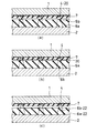
図1は本発明の第1の実施例に係るプラズマディスプレイパネルの構造を示す模式図である。 FIG. 1 is a schematic diagram showing the structure of a plasma display panel according to a first embodiment of the present invention.
ガラス基板1上に矩形の複数個の透明電極膜3がマトリクス状に配設されている。透明電極膜3は、例えばITO透明導電体薄膜を細長く短冊状にパタン化することにより形成される。本実施例における水平及び垂直方向の画素ピッチはいずれも、例えば0.81mmであり、矩形の透明電極膜3の寸法は、例えば垂直方向で0.74mm、水平方向で0.19mmであり、そのピッチは、例えば垂直方向で0.81mm、水平方向で0.27mmであるが、本発明はこれらに限定されるものではない。
A plurality of rectangular
また、行をなす複数個の透明電極膜3の中央部を連ねるように水平方向に延びる複数本のバス電極4が設けられている。透明電極膜3のバス電極4の両側にはみ出した部分が表示放電電極8となっている。このようにして、バス電極4からその両側に表示放電電極8が延出した構造の両側面放電電極300が構成されている。バス電極4を介して外部から表示放電電極8に電力が供給される。なお、バス電極4は、例えば感光性銀厚膜から形成されており、その幅は、例えば0.1mmである。また、バス電極4は、表示のコントラストを高めるため、例えば表示側に設けられた黒色層とその上に設けられた低抵抗の白色層とからなる黒白2層の積層構造を有している。
A plurality of
更に、ガラス基板1上には、透明電極膜3及びバス電極4からなる両側面放電電極300を被覆しグレーズ層及びMgO表面保護層からなる透明な誘電体層7が形成されている。このようにして、前面基板100が構成されている。
Further, a
一方、前面基板100と平行に配設される背面基板200においては、ガラス基板2上に垂直方向に延びる複数本のデータ電極5が形成されている。データ電極5は、例えばガラス基板2上にアルミニウム薄膜をスパッタリングにより形成し、これをエッチングでパタン化することにより形成することができる。データ電極5の幅は、例えば0.09mmであり、そのピッチは、例えば0.27mmである。
On the other hand, in the
また、ガラス基板2上には、データ電極5を被覆する誘電体層7が形成され、誘電体層7上に垂直方向に延びる垂直隔壁6a及び水平方向に延びる水平隔壁6bからなる井桁状の隔壁が形成されている。誘電体層10は低融点ガラスを主成分としている。また、垂直隔壁6a及び水平隔壁6bは、例えばサンドブラスト法により形成され、垂直隔壁6aの上部の幅は、例えば約40μm、隔壁6bの上部の幅は、例えば約100μmであるが、本発明はこれらに限定されるものではない。
A
更に、隔壁6a及び6bにより区画された複数個の凹状部の底部及び側面に蛍光体粉末からなり赤色、緑色又は青色に発光する蛍光体層9が塗布されている。蛍光体層9の発光色は上述の順で水平方向に並んでいる。このようにして、背面基板200が構成されている。
Further, a
そして、背面基板200と前面基板100とが組み合わされ、両基板の周囲がフリットガラスで封着され、加熱排気された後に希ガスを主成分とする放電ガスが封入されている。このようにして、カラープラズマディスプレイパネルが構成されている。なお、背面基板200と前面基板100とは、図1に示すように、平面視でバス電極4が水平隔壁6bに重なり、且つ、水平方向で隣接する表示放電電極8間の隙間が垂直隔壁6aに重なるように、垂直方向及び水平方向の目合わせを行って組み立てられている。
The
このように構成された第1の実施例においては、表示放電電極8に電力を供給するバス電極4が平面視で水平隔壁6bと重なり、水平方向で隣接する表示セル間において表示放電電極8が分離されているので、後述の簡単な駆動方法により、広い駆動マージンを確保することができる。また、開口率が高く、表示放電電極8の面積を広くとることができるため、高輝度が得られる。
In the first embodiment configured as described above, the
なお、水平方向で隣接する表示セル間において表示放電電極が実効的に分離されていれば、その形状は特に矩形に限定されるものではない。以下、第1の実施例における表示放電電極を変形した第2乃至第5の実施例について説明する。図2(a)は第2の実施例における表示放電電極を示す模式的平面図、(b)は第3の実施例における表示放電電極を示す模式的平面図、(c)は第4の実施例における表示放電電極を示す模式的平面図、(d)は第5の実施例における表示放電電極を示す模式的平面図である。 Note that the shape is not particularly limited to a rectangle as long as the display discharge electrodes are effectively separated between display cells adjacent in the horizontal direction. Hereinafter, second to fifth embodiments in which the display discharge electrodes in the first embodiment are modified will be described. 2A is a schematic plan view showing the display discharge electrode in the second embodiment, FIG. 2B is a schematic plan view showing the display discharge electrode in the third embodiment, and FIG. 2C is the fourth implementation. FIG. 5D is a schematic plan view showing a display discharge electrode in an example, and FIG. 6D is a schematic plan view showing a display discharge electrode in a fifth embodiment.
第2の実施例においては、図2(a)に示すように、形状が櫛歯状の透明電極膜3−2が設けられており、この櫛歯の軸部から突出する部分が表示放電電極8−2となっている。そして、櫛歯の軸部にバス電極4が整合している。
In the second embodiment, as shown in FIG. 2A, a comb-like transparent electrode film 3-2 is provided, and a portion protruding from the comb-shaped shaft portion is a display discharge electrode. 8-2. The
このように構成された第2の実施例においては、第1の実施例と比して、バス電極4と表示放電電極8−2を構成する透明電極膜3−2との接触面積が広いので、これらの間の電気的接続が改善され、暗点の防止に有効である。
In the second embodiment configured as described above, the contact area between the
第3の実施例においては、図2(b)に示すように、透明電極膜3−3の両端部の幅が中央部の幅よりも広くなるように形成されている。つまり、バス電極4との接続部の幅よりも先端部の幅が広くなるように形成された表示放電電極8−3が設けられている。
In the third embodiment, as shown in FIG. 2 (b), the transparent electrode film 3-3 is formed such that the width of both end portions is wider than the width of the central portion. In other words, the display discharge electrode 8-3 formed so that the width of the tip end portion is wider than the width of the connection portion with the
パネル製造工程において、透明電極とバス電極との相対位置がずれたり、水平隔壁がバス電極又は透明電極の中央部からずれることがあるが、図1に示す第1の実施例のような単純な矩形電極では、ずれに応じて表示放電電極の面積がバス電極の上側と下側とで不均等になる。面放電の強さは面積が狭い方の電極により影響を受けるため、ずれの大きさと共に輝度が低下する。これに対し、図2(b)に示す第3の実施例のように、バス電極4との接続部の近傍で表示放電電極8−3の幅が狭くなっている場合は、ずれが生じても電極面積の変化は少なくなる。例えば、バス電極4近傍の表示放電電極8−3の幅が先端の幅広部の3分の1となっている場合には、同じずれに対して、輝度の変化量は3分の1に低減され、ずれに対するマージンを大きくすることができる。また、バス電極4及び水平隔壁6bに近い領域への放電の広がりが少ないため、発光効率が改善されるという効果もある。
In the panel manufacturing process, the relative position between the transparent electrode and the bus electrode may be displaced, or the horizontal partition may be displaced from the central portion of the bus electrode or the transparent electrode. However, as in the first embodiment shown in FIG. In the rectangular electrode, the area of the display discharge electrode becomes uneven between the upper side and the lower side of the bus electrode according to the shift. Since the intensity of the surface discharge is affected by the electrode having the smaller area, the luminance decreases with the magnitude of the deviation. On the other hand, when the width of the display discharge electrode 8-3 is narrow in the vicinity of the connection portion with the
第4の実施例においては、図2(c)に示すように、表示放電電極8−4がバス電極4に接続され幅が狭く導電性が高い金属パタン3−4b及びこれに接続された矩形の透明電極膜3−4aから構成されている。金属パタン3−4bは、例えばバス電極4のパタン化と同時にパタン化すればよい。
In the fourth embodiment, as shown in FIG. 2C, the display discharge electrode 8-4 is connected to the
このように構成された第4の実施例においても、第3の実施例と同様に、ずれマージンの増大が可能であり、発光効率の改善が実現される。 Also in the fourth embodiment configured as described above, as in the third embodiment, the deviation margin can be increased, and the light emission efficiency can be improved.
第5の実施例においては、図2(d)に示すように、表示放電電極8−5がメッシュ状にパタン化して形成されている。 In the fifth embodiment, as shown in FIG. 2D, the display discharge electrode 8-5 is formed in a mesh pattern.
このように構成された第5の実施例においては、表示放電電極8−5に透明電極が使用されていないので、製造工程を簡略化することができる。即ち、バス電極4のパタン化と同時に金属薄膜をパタン化すればよい。
In the fifth embodiment configured as described above, since the transparent electrode is not used for the display discharge electrode 8-5, the manufacturing process can be simplified. That is, the metal thin film may be patterned simultaneously with the patterning of the
なお、表示放電電極の形状は、図1及び図2(a)乃至(d)に示した第1乃至第5の実施例のものよりも更に複雑な形状としてもよい。 The shape of the display discharge electrode may be more complicated than that of the first to fifth embodiments shown in FIGS. 1 and 2A to 2D.
次に、本発明の第6乃至第10の実施例について説明する。第6乃至第10の実施例においては、バス電極に接続された表示放電電極の形状が当該バス電極の垂直上側と垂直下側とで互いに異なっている。以下、第1乃至第5の実施例に係るプラズマディスプレイパネルを対称パネルといい、第6乃至第10の実施例に係るプラズマディスプレイパネルを非対称パネルという。図3(a)は第6の実施例における表示放電電極を示す模式的平面図、(b)は第7の実施例における表示放電電極を示す模式的平面図、(c)は第8の実施例における表示放電電極を示す模式的平面図、(d)は第9の実施例における表示放電電極を示す模式的平面図、(e)は第10の実施例における表示放電電極を示す模式的平面図である。 Next, sixth to tenth embodiments of the present invention will be described. In the sixth to tenth embodiments, the shape of the display discharge electrode connected to the bus electrode is different between the vertical upper side and the vertical lower side of the bus electrode. Hereinafter, the plasma display panels according to the first to fifth embodiments are referred to as symmetric panels, and the plasma display panels according to the sixth to tenth embodiments are referred to as asymmetric panels. 3A is a schematic plan view showing the display discharge electrode in the sixth embodiment, FIG. 3B is a schematic plan view showing the display discharge electrode in the seventh embodiment, and FIG. 3C is the eighth implementation. The schematic plan view which shows the display discharge electrode in an example, (d) is a schematic plan view which shows the display discharge electrode in a 9th Example, (e) is the schematic plane which shows the display discharge electrode in a 10th Example. FIG.
第6の実施例においては、図3(a)に示すように、パネルの垂直方向において幅が2段階に変化している透明電極膜3−6が設けられている。具体的には、各透明電極膜3−6の上半分の幅が下半分の幅よりも広くなっている。そして、第1の実施例と同様に、バス電極4が行をなす複数個の透明電極膜3−6の中央部分に接続されている。このような透明電極膜3−6から、バス電極4からその垂直上側に延出する表示放電電極8−6a及び垂直下側に延出する表示放電電極8−6bが形成され、表示放電電極8−6aの幅が表示放電電極8−6bの幅よりも広くなっている。
In the sixth embodiment, as shown in FIG. 3A, a transparent electrode film 3-6 whose width changes in two stages in the vertical direction of the panel is provided. Specifically, the width of the upper half of each transparent electrode film 3-6 is wider than the width of the lower half. As in the first embodiment, the
このように構成された第6の実施例においては、1個の表示セルに関して、垂直上側に位置する表示放電電極8−6bの幅が垂直下側に位置する表示放電電極8−6aの幅よりも狭くなる。このため、表示放電電極8−6aの方が対向放電開始電圧が低く、背面基板に設けられたデータ電極との間での対向放電が発生しやすい。このため、1個の表示セル内に設けられた2個の表示放電電極8−6a及び8−6bの対向放電開始電圧の中間電圧のパルスを印加すれば、垂直下側に位置する表示放電電極8−6aとデータ電極との間でのみ対向放電を生じさせることができる。従って、後述の簡単な駆動方法により、広い駆動マージンを確保することができる。 In the sixth embodiment configured as described above, the width of the display discharge electrode 8-6b positioned vertically above the width of the display discharge electrode 8-6a positioned vertically below is related to one display cell. Becomes narrower. For this reason, the counter discharge start voltage is lower in the display discharge electrode 8-6a, and a counter discharge is easily generated between the display discharge electrode 8-6a and the data electrode provided on the back substrate. For this reason, if a pulse of an intermediate voltage of the counter discharge start voltage of the two display discharge electrodes 8-6a and 8-6b provided in one display cell is applied, the display discharge electrode positioned vertically downward A counter discharge can be generated only between 8-6a and the data electrode. Therefore, a wide driving margin can be secured by a simple driving method described later.
第7の実施例においては、図3(b)に示すように、パネルの垂直方向において幅が4段階に変化している透明電極膜3−7が設けられている。具体的には、各透明電極膜3−7は垂直方向の中央部で2分割され、更にこれらが2分割され、最上部の幅よりもその下の部分の幅が狭く、最下部の幅よりもその上の部分の幅が広く、最上部と最下部とを比較すると、最上部の幅の方が最下部の幅よりも広くなっている。そして、第1の実施例と同様に、バス電極4が行をなす複数個の透明電極膜3−7の中央部分に接続されている。このような透明電極膜3−7から、バス電極4からその垂直上側に延出する表示放電電極8−7a及び垂直下側に延出する表示放電電極8−7bが形成され、表示放電電極8−7aの端部の幅が表示放電電極8−7bの端部の幅よりも広くなっている。
In the seventh embodiment, as shown in FIG. 3B, a transparent electrode film 3-7 whose width changes in four steps in the vertical direction of the panel is provided. Specifically, each transparent electrode film 3-7 is divided into two at the central portion in the vertical direction, and further divided into two, the width of the lower portion is narrower than the width of the uppermost portion, and the width of the lowermost portion. Also, the width of the upper part is wide, and when the uppermost part and the lowermost part are compared, the width of the uppermost part is wider than the width of the lowermost part. As in the first embodiment, the
このように構成された第7の実施例においては、1個の表示セルに関して、垂直上側に位置する表示放電電極8−7bの端部の幅が垂直下側に位置する表示放電電極8−7aの端部の幅よりも狭くなる。このため、表示放電電極8−7aの方が対向放電開始電圧が低く、背面基板に設けられたデータ電極との間での対向放電が発生しやすい。従って、第6の実施例と同様に、後述の簡単な駆動方法により、広い駆動マージンを確保することができる。 In the seventh embodiment thus configured, the display discharge electrode 8-7a in which the width of the end portion of the display discharge electrode 8-7b positioned on the upper vertical side is positioned on the lower vertical side with respect to one display cell. It becomes narrower than the width of the end of the. For this reason, the counter discharge start voltage is lower in the display discharge electrode 8-7a, and the counter discharge is easily generated between the display electrode 8-7a and the data electrode provided on the back substrate. Therefore, similarly to the sixth embodiment, a wide driving margin can be ensured by a simple driving method described later.
第8の実施例においては、図3(c)に示すように、下端部に開口部が形成された透明電極膜3−8が設けられている。そして、第1の実施例と同様に、バス電極4が行をなす複数個の透明電極膜3−8の中央部分に接続されている。このような透明電極膜3−8から、バス電極4からその垂直上側に延出する表示放電電極8−8a及び垂直下側に延出しその端部に開口部が設けられた表示放電電極8−8bが形成されている。
In the eighth embodiment, as shown in FIG. 3C, a transparent electrode film 3-8 having an opening formed at the lower end is provided. As in the first embodiment, the
このように構成された第8の実施例においては、1個の表示セルに関して、垂直上側に位置する表示放電電極8−8bの先端部の断面積が、開口部の分だけ垂直下側に位置する表示放電電極8−8aの先端部の断面積よりも狭くなる。このため、表示放電電極8−8aの方が対向放電開始電圧が低く、背面基板に設けられたデータ電極との間での対向放電が発生しやすい。従って、第6の実施例と同様に、後述の簡単な駆動方法により、広い駆動マージンを確保することができる。 In the eighth embodiment configured as described above, with respect to one display cell, the cross-sectional area of the tip of the display discharge electrode 8-8b positioned on the vertical upper side is positioned on the vertical lower side by the amount corresponding to the opening. It becomes narrower than the cross-sectional area of the tip of the display discharge electrode 8-8a. For this reason, the counter discharge start voltage is lower in the display discharge electrode 8-8a, and the counter discharge between the data electrodes provided on the rear substrate is likely to occur. Therefore, similarly to the sixth embodiment, a wide driving margin can be ensured by a simple driving method described later.
第9の実施例においては、図3(d)に示すように、メッシュ状の金属薄膜からなる部分とその上端に設けられメッシュが形成されていない金属薄膜からなる部分とにより構成された網状金属膜3−9が設けられている。そして、第1の実施例と同様に、バス電極4が行をなす複数個の網状金属膜3−9の中央部分に接続されている。このような網状金属膜3−9から、バス電極4からその垂直上側に延出し端部にメッシュが設けられていない表示放電電極8−9a及び垂直下側に延出する表示放電電極8−8bが形成されている。
In the ninth embodiment, as shown in FIG. 3 (d), a net-like metal composed of a portion made of a mesh-like metal thin film and a portion made of a metal thin film provided at the upper end of which is not formed with a mesh. A membrane 3-9 is provided. As in the first embodiment, the
このように構成された第9の実施例においては、1個の表示セルに関して、垂直上側に位置する表示放電電極8−9bの先端部の断面積が、メッシュが形成された分だけ垂直下側に位置する表示放電電極8−9aの先端部のメッシュが形成されていない部分の断面積よりも狭くなる。このため、表示放電電極8−9aの方が対向放電開始電圧が低く、背面基板に設けられたデータ電極との間での対向放電が発生しやすい。従って、第6の実施例と同様に、後述の簡単な駆動方法により、広い駆動マージンを確保することができる。 In the ninth embodiment configured as described above, the cross-sectional area of the tip portion of the display discharge electrode 8-9b positioned on the vertical upper side of one display cell is vertically lower by the amount of the mesh formed. It becomes narrower than the cross-sectional area of the part in which the mesh of the front-end | tip part of the display discharge electrode 8-9a located in is not formed. For this reason, the counter discharge start voltage is lower in the display discharge electrode 8-9a, and the counter discharge is easily generated between the display electrode 8-9a and the data electrode provided on the back substrate. Therefore, similarly to the sixth embodiment, a wide driving margin can be ensured by a simple driving method described later.
第10の実施例においては、図3(e)に示すように、第7の実施例における表示放電電極8−7の上下方向の向きが1列毎に反転している。この場合にも、第7の実施例と同様の効果が得られる。但し、第10の実施例のための駆動方法は、第7の実施例のための駆動方法と相違することになる。 In the tenth embodiment, as shown in FIG. 3E, the vertical direction of the display discharge electrode 8-7 in the seventh embodiment is reversed for each column. In this case, the same effect as that of the seventh embodiment can be obtained. However, the driving method for the tenth embodiment is different from the driving method for the seventh embodiment.
なお、1個の表示セルに関し、2個の表示放電電極間の形状が相違し、それらの対向放電特性が互いに異なっていれば、表示放電電極の形状は、図3(a)乃至(e)に示した第6乃至第10の実施例のものよりも更に複雑な形状としてもよい。 If one display cell has a different shape between the two display discharge electrodes and their opposite discharge characteristics are different from each other, the shape of the display discharge electrode is as shown in FIGS. The shape may be more complicated than those of the sixth to tenth embodiments shown in FIG.
また、表示放電電極の長さも異なっていてもよい。 Further, the lengths of the display discharge electrodes may be different.
次に、本発明の第11及び第12の実施例について説明する。第6乃至第10の実施例においては、1個の表示セルに関して2個の表示放電電極の形状を互いに異なるものとすることにより、それらの対向放電特性を異なるものとしているが、第11及び第12の実施例においては、前面基板側の誘電体膜の形状を2個の表示放電電極上で互いに異なるものとしている。図4は本発明の第11の実施例に係るプラズマディスプレイパネルを示す図であって、(a)は模式的平面図であり、(b)は(a)のA−A線に沿った断面図である。また、図5は本発明の第12の実施例に係るプラズマディスプレイパネルを示す図であって、(a)は模式的平面図であり、(b)は(a)のB−B線に沿った断面図である。但し、図4(a)及び(b)並びに図5(a)及び(b)では、所望の構成物を明確に表すために、一部の構成物を省略しているため、一方に記載されていても、他方に記載されていないものもある。 Next, eleventh and twelfth embodiments of the present invention will be described. In the sixth to tenth embodiments, the shape of the two display discharge electrodes for one display cell is made different from each other, so that their counter discharge characteristics are different. In the twelfth embodiment, the shape of the dielectric film on the front substrate side is different from each other on the two display discharge electrodes. 4A and 4B are views showing a plasma display panel according to an eleventh embodiment of the present invention, in which FIG. 4A is a schematic plan view, and FIG. 4B is a cross section taken along line AA in FIG. FIG. FIG. 5 is a view showing a plasma display panel according to a twelfth embodiment of the present invention, wherein (a) is a schematic plan view, and (b) is taken along line BB in (a). FIG. However, in FIGS. 4 (a) and 4 (b) and FIGS. 5 (a) and 5 (b), some components are omitted in order to clearly represent the desired components. Some of them are not listed on the other.
第11の実施例においては、図4(a)及び(b)に示すように、ITO薄膜等の透明導電膜からなる透明電極膜3の垂直下側端部の上に厚さ方向に突出する金属製のドット21が設けられている。このドット21は、バス電極4を感光性銀ペーストにより形成する際に、同時に感光性銀ペーストをパタン化することにより、容易に形成することができる。ドット21の厚さは、例えば8μm程度である。表示放電電極8を覆う誘電体層7−11がガラス基板1上に形成されているが、ドット21が形成された位置において、誘電体層7−11は、他の部分よりもやや盛り上がっている。この部分の誘電体層7−11の厚さは、透明電極膜3のドット21が形成されていない領域に整合する部分の厚さよりも、例えば5μm程度薄くなっている。
In the eleventh embodiment, as shown in FIGS. 4A and 4B, the projection protrudes in the thickness direction on the vertical lower end of the
このように構成された第11の実施例においては、1個の表示セルに関して、垂直上側に位置する表示放電電極8−11bの先端部にドット21が設けられ、垂直下側に位置する表示放電電極8−11aにはドットが設けられず、更に、その部分に整合する誘電体層7−11の厚さが他の部分の厚さよりも薄くなっているので、表示放電電極8−11bの方が対向放電開始電圧が低くなる。
In the eleventh embodiment configured in this way, with respect to one display cell, a
なお、ドット21のような表示放電電極上に設けられた電気伝導性を具備した突起部分は、広い方が対向放電開始電圧を低下させる効果は大きいが、突起部分は蛍光体層からの発光を遮蔽するため、余り大きくすることは得策ではない。より小さい突起で放電開始電圧を低下させる効果を得るためには、面放電ギャップに近い位置に設けることが好ましい。
In addition, although the protrusion part provided with the electrical conductivity provided on the display discharge electrode such as the
第12の実施例においては、図5(a)及び(b)に示すように、表示放電電極8を覆う誘電体層7−12がガラス基板1上に形成されている。この誘電体層7−12の表示放電電極8の垂直下側端部に整合する部分の厚さは、他の部分の厚さよりも薄くなっている。例えば、その部分の厚さは20μm程度であり、他の部分の厚さは30μm程度である。このような形状の誘電体層7−12は、例えばグレーズ層のパターン印刷、感光性グレーズペーストの利用又はグレーズ層のパターンエッチング等の方法により形成することができる。
In the twelfth embodiment, as shown in FIGS. 5A and 5B, a dielectric layer 7-12 that covers the
このように構成された第12の実施例においては、1個の表示セルに関して、誘電体層7−12の垂直上側に位置する表示放電電極8を覆う部分の厚さが垂直下側に位置する表示放電電極8を覆う部分の厚さよりも薄くなっており、一般に誘電体層の厚さが薄い程、データ電極との対向放電開始電圧が低くなるため、表示放電電極8の方が対向放電開始電圧が低くなる。
In the twelfth embodiment configured as described above, the thickness of the portion covering the
なお、1個の表示セルに関して、一方の表示放電電極を覆う誘電体層の部分を全体的に薄くしてもよいが、対向放電特性を2個の表示放電電極間で互いに異なるものとするためには、誘電体層の一部分だけを薄くしてもよい。また、図5(a)及び(b)に示す第12の実施例では、誘電体層7−12に厚さが薄い部分がドット状に形成されているが、水平方向に延びる帯状に薄膜部分が形成されていてもよい。この場合、特に面放電ギャップに近い部位で誘電体層を薄くすれば、より高い効果が得られる。 For one display cell, the portion of the dielectric layer covering one display discharge electrode may be thinned as a whole, but the counter discharge characteristics are different between the two display discharge electrodes. Alternatively, only a part of the dielectric layer may be thinned. Further, in the twelfth embodiment shown in FIGS. 5A and 5B, the thin portion of the dielectric layer 7-12 is formed in a dot shape, but the thin film portion is formed in a strip shape extending in the horizontal direction. May be formed. In this case, a higher effect can be obtained if the dielectric layer is thinned particularly at a portion close to the surface discharge gap.
更に、第11及び第12の実施例のように誘電体層の形状に特徴を持たせるのではなく、誘電体層の特性に特徴を持たせることによっても、1個の表示セル内に設けられた2個の表示放電電極間の対向放電特性に違いを持たせることができる。例えば、一方の表示放電電極上の誘電体層の表面の2次電子放出係数と他方の表示放電電極上の誘電体層表面の2次電子放出係数との間に差を設けてもよい。具体的には、一方には酸化マグネシウム膜を形成し、他方には酸化マグネシウム膜を形成しないか、又は2次電子放出係数が小さいアルミナ膜等を形成した構造等としてもよい。 Further, the characteristic of the dielectric layer is not provided as in the eleventh and twelfth embodiments, but the characteristic of the dielectric layer is provided in one display cell. In addition, it is possible to make a difference in the counter discharge characteristics between the two display discharge electrodes. For example, a difference may be provided between the secondary electron emission coefficient on the surface of the dielectric layer on one display discharge electrode and the secondary electron emission coefficient on the surface of the dielectric layer on the other display discharge electrode. Specifically, a structure in which a magnesium oxide film is formed on one side and a magnesium oxide film is not formed on the other side, or an alumina film or the like having a small secondary electron emission coefficient may be formed.
次に、本発明の第13乃至第19の実施例について説明する。第13乃至第17の実施例においては、背面基板側のデータ電極の形状を1個の表示セル内において夫々2個の表示放電電極に整合する領域で互いに異なるものとしている。図6(a)は第13の実施例におけるデータ電極を示す模式的平面図、(b)は第14の実施例におけるデータ電極を示す模式的平面図、(c)は第15の実施例におけるデータ電極を示す模式的平面図、(d)は第16の実施例におけるデータ電極を示す模式的平面図、(e)は第19の実施例におけるデータ電極を示す模式的平面図である。図7(a)は第16の実施例の構造を示す断面図、(b)は第17の実施例の構造を示す断面図、(c)は第18の実施例の構造を示す断面図である。 Next, thirteenth through nineteenth embodiments of the present invention will be described. In the thirteenth to seventeenth embodiments, the shape of the data electrode on the rear substrate side is different from each other in a region that matches two display discharge electrodes in one display cell. 6A is a schematic plan view showing a data electrode in the thirteenth embodiment, FIG. 6B is a schematic plan view showing a data electrode in the fourteenth embodiment, and FIG. 6C is a diagram in the fifteenth embodiment. FIG. 14D is a schematic plan view showing the data electrode, FIG. 14D is a schematic plan view showing the data electrode in the sixteenth embodiment, and FIG. 9E is a schematic plan view showing the data electrode in the nineteenth embodiment. 7A is a sectional view showing the structure of the sixteenth embodiment, FIG. 7B is a sectional view showing the structure of the seventeenth embodiment, and FIG. 7C is a sectional view showing the structure of the eighteenth embodiment. is there.
第13の実施例においては、図6(a)に示すように、垂直方向に延びるデータ電極5−13が設けられている。データ電極5−13の幅は、表示放電電極8のバス電極4から垂直下側に延出する部分に整合する領域において他の領域よりも広くなっている。例えば、データ電極5−13の狭い部分の幅は60μmであり、広い部分の幅は190μmである。
In the thirteenth embodiment, as shown in FIG. 6A, a data electrode 5-13 extending in the vertical direction is provided. The width of the data electrode 5-13 is wider than the other regions in the region aligned with the portion of the
一般に表示放電電極と重なるデータ電極の幅が狭いほど、対向放電開始電圧が低いので、上述のように構成された第13の実施例においては、1個の表示セルに関して、垂直上側に位置する表示放電電極8との間の対向放電開始電圧の方が低くなる。データ電極5−13の幅が上述のようなものであれば、例えば対向放電開始電圧に20Vの差が得られる。
In general, as the width of the data electrode overlapping the display discharge electrode is narrower, the counter discharge start voltage is lower. Therefore, in the thirteenth embodiment configured as described above, the display positioned vertically above with respect to one display cell. The counter discharge start voltage with respect to the
第14の実施例においては、図6(b)に示すように、垂直方向に延びるデータ電極5−14が水平方向で隣接する表示セル間に設けられている。即ち、データ電極5−14は、垂直隔壁(図示せず)の下に設けられている。データ電極5−14には、表示放電電極8のバス電極4から垂直下側に延出する部分に整合する領域まで突き出た部分が設けられている。従って、表示放電電極8のバス電極4から垂直下側に延出する部分とデータ電極5−14とは、平面視で第1の実施例よりも広い面積で重なっている一方で、表示放電電極8のバス電極4から垂直上側に延出する部分とデータ電極5−14とは重なっていない。
In the fourteenth embodiment, as shown in FIG. 6B, data electrodes 5-14 extending in the vertical direction are provided between display cells adjacent in the horizontal direction. That is, the data electrode 5-14 is provided under a vertical partition (not shown). The data electrode 5-14 is provided with a portion that protrudes to a region that matches the portion that extends vertically downward from the
このように構成された第14の実施例においては、バス電極4から垂直上側に延出する表示放電電極8と垂直隔壁の下に配置されたデータ電極5−14との間の対向放電の開始電圧が極めて高いため、この対向放電開始電圧とバス電極から垂直下側に延出する表示放電電極8とデータ電極5−14との間の対向放電開始電圧との差を大きくとることができる。
In the fourteenth embodiment configured as described above, the counter discharge between the
第15の実施例においては、図6(c)に示すように、列をなす表示セルの両側に位置する垂直隔壁6a間で蛇行するデータ電極5−15が設けられている。データ電極5−15は、各表示セルにおいてバス電極4から垂直下側に延出する表示放電電極8の下方を横切っている。そして、データ電極5−15には、表示放電電極8を横切る領域に幅が広い膨大部が形成されている。
In the fifteenth embodiment, as shown in FIG. 6C, data electrodes 5-15 meandering between the
このように構成された第15の実施例においては、図6(b)に示す第14の実施例と同様、バス電極4から垂直上側に延出する表示放電電極8については、その下方に設けられたデータ電極5−15の幅が狭く、データ電極5−15自体は垂直隔壁6aの下に配置されているため、この領域での対向放電開始電圧はバス電極4から下側に延出する表示放電電極8とデータ電極の表示放電電極8を横切る領域との間の対向放電開始電圧と比して極めて高くなる。なお、データ電極の表示放電電極8を横切る領域には、図6(c)に示した膨大部は必ずしも必要ではないが、適当な面積の膨大部を設ける方が、より対向放電を生じやすくすることができるので、より有効である。
In the fifteenth embodiment configured as described above, as in the fourteenth embodiment shown in FIG. 6B, the
第13乃至第15の実施例では、データ電極の平面的な形状が調整されているが、これらに対し、背面基板等の製造工程が複雑になるものの、放電開始電圧を高く設定する予定の部位のデータ電極を他の部位より表示放電電極から離間して配置して表示放電電極との距離を長くしたり、その部位の誘電体層を厚くしたりする等の立体的構造によっても、バス電極の一方の表示放電電極とデータ電極との間の放電開始電圧を高くすることができる。第16乃至第18の実施例は、このような立体的構造を採用した実施例である。 In the thirteenth to fifteenth embodiments, the planar shape of the data electrode is adjusted. On the other hand, the manufacturing process of the back substrate and the like is complicated, but the part where the discharge start voltage is to be set high. The bus electrode is also provided by a three-dimensional structure such as increasing the distance from the display discharge electrode by arranging the data electrode away from the display discharge electrode from other parts and increasing the dielectric layer of the part. The discharge start voltage between one of the display discharge electrodes and the data electrode can be increased. The sixteenth to eighteenth examples are examples in which such a three-dimensional structure is adopted.
第16の実施例においては、図6(d)及び図7(a)に示すように、水平方向に延びる領域Aにおいて他の領域よりも前面基板側に近づくよう段差が設けられたデータ電極5−16が形成されている。なお、領域Aは、各表示セル内で垂直上側に位置する表示放電電極8と直交している。
In the sixteenth embodiment, as shown in FIGS. 6D and 7A, the
このように構成された第16の実施例においては、データ電極5−16に段差が形成されているため、1個の表示セルに関して、垂直上側に位置する表示放電電極8とデータ電極5−16との間の距離は、下側に位置する表示放電電極8とデータ電極5−16との間の距離よりも狭くなる。従って、データ電極5−16と垂直上側に位置する表示放電電極8との間の対向放電開始電圧の方が低くなる。
In the sixteenth embodiment configured as described above, since a step is formed in the data electrode 5-16, the
第17の実施例においては、図7(b)に示すように、水平方向に延びる領域Aに窪み10−17aが設けられた誘電体層10−17が設けられている。 In the seventeenth embodiment, as shown in FIG. 7B, a dielectric layer 10-17 having a recess 10-17a is provided in a region A extending in the horizontal direction.
このように構成された第17の実施例においては、1個の表示セルに関して、バス電極4の垂直上側と垂直下側とで表示放電電極8とデータ電極5との間の距離は等しいが、それらの間に存在する誘電体層10−17については、垂直上側の方が薄くなる。従って、データ電極5と垂直上側に位置する表示放電電極8との間の対向放電開始電圧の方が低くなる。
In the seventeenth embodiment configured as described above, the distance between the
第18の実施例においては、図7(c)に示すように、領域Aに誘電体層10−18aが形成され、それ以外の領域に誘電体層10−18bが形成されている。誘電体層10−18bの誘電率は、誘電体層10−18aのそれよりも高いものである。 In the eighteenth embodiment, as shown in FIG. 7C, the dielectric layer 10-18a is formed in the region A, and the dielectric layer 10-18b is formed in the other regions. The dielectric constant of the dielectric layer 10-18b is higher than that of the dielectric layer 10-18a.
このように構成された第18の実施例においては、1個の表示セルに関して、バス電極4の垂直上側と垂直下側とで表示放電電極8とデータ電極5との間の距離は等しいが、それらの間に存在する誘電体層10−18a及び10−18bの誘電率が異なるので、データ電極5と垂直上側に位置する表示放電電極8との間の対向放電開始電圧の方が低くなる。
In the eighteenth embodiment configured as described above, the distance between the
また、第13乃至第18の実施例においては、表示セル内で垂直上側の表示放電電極とデータ電極との間の放電開始電圧が低くされているが、配置を逆にして表示セル内で垂直下側の表示放電電極とデータ電極との間の放電開始電圧を低くしてもよい。更に、データ電極の幅広部分が、バス電極の上側の表示放電電極側への配置と下側の表示電極側への配置とが1列毎に逆転し、1列毎に放電開始電圧の低い領域が逆転していてもよい。第19の実施例は、このような配置を採用した実施例である。 In the thirteenth to eighteenth embodiments, the discharge start voltage between the display discharge electrode and the data electrode on the upper vertical side in the display cell is lowered, but the arrangement is reversed and the discharge start voltage is vertical in the display cell. The discharge start voltage between the lower display discharge electrode and the data electrode may be lowered. Furthermore, the wide portion of the data electrode is a region where the arrangement of the bus electrode on the upper display discharge electrode side and the lower display electrode side is reversed for each column and the discharge start voltage is low for each column. May be reversed. The nineteenth embodiment is an embodiment that employs such an arrangement.
第19の実施例においては、図6(e)に示すように、第13の実施例におけるデータ電極5−13の上下方向の向きが1列毎に反転したデータ電極5−19が形成されている。この場合にも、このような配置に合わせて、駆動方法及び映像データ配列を整合させれば、第13の実施例等と同様の効果が得られる。 In the nineteenth embodiment, as shown in FIG. 6E, a data electrode 5-19 is formed in which the vertical direction of the data electrode 5-13 in the thirteenth embodiment is inverted every column. Yes. Also in this case, the same effect as that of the thirteenth embodiment can be obtained by matching the driving method and the video data arrangement in accordance with such an arrangement.
1個の表示セルに関して、第6乃至第10の実施例では、2個の表示放電電極の形状を互いに異なるものとし、第11及び第12の実施例では、誘電体層の厚さを互いに異なるものとし、第13乃至第19の実施例では、データ電極等の形状又は誘電体層の特性を互いに異なるものとすることにより、表示放電電極とデータ電極との間の対向放電開始電圧及び放電強度の強さ等に差を付与しているが、これらの実施例を組み合わせることにより、対向放電開始電圧により大きな差を付けることができる。なお、実用的にはパネルの均一性等の関係で、表示セル内で放電開始電圧の差は20V以上が確保されるように設計することが好ましい。 Regarding one display cell, the shapes of the two display discharge electrodes are different from each other in the sixth to tenth embodiments, and the thicknesses of the dielectric layers are different from each other in the eleventh and twelfth embodiments. In the thirteenth to nineteenth embodiments, the opposing discharge start voltage and discharge intensity between the display discharge electrode and the data electrode are made different from each other in the shape of the data electrode or the like or the characteristics of the dielectric layer. Although a difference is given to the strength of the above, a large difference can be given to the counter discharge start voltage by combining these embodiments. In practice, it is preferable to design the display cell so that the difference in the discharge start voltage is 20 V or more in view of the uniformity of the panel.
次に、本発明の第20乃至第22の実施例について説明する。第18乃至第20の実施例においては、垂直隔壁と前面基板との間に隙間が形成されている。図8(a)は第20の実施例に係るプラズマディスプレイパネルを示す断面図、(b)は第21の実施例に係るプラズマディスプレイパネルを示す断面図、(c)は第22の実施例に係るプラズマディスプレイパネルを示す断面図である。 Next, twentieth to twenty-second embodiments of the present invention will be described. In the eighteenth to twentieth embodiments, a gap is formed between the vertical partition and the front substrate. 8A is a sectional view showing a plasma display panel according to the twentieth embodiment, FIG. 8B is a sectional view showing a plasma display panel according to the twenty-first embodiment, and FIG. 8C is a sectional view showing the twenty-second embodiment. It is sectional drawing which shows the plasma display panel which concerns.
第20の実施例においては、図8(a)に示すように、厚さが前述の第1乃至第19の実施例におけるものよりも2倍程度厚いバス電極4−20が設けられている。バス電極4−20の厚さは、例えば約10μmである。バス電極4−20は、平面視で水平隔壁6bと重なっている。そして、バス電極4−20を覆う誘電体層7がガラス基板2上に形成されている。誘電体層7の厚さは、例えば約25μmであるが、バス電極4−20と重なる部分と重ならない部分とでは、約7μmの段差が存在する。このため、背面基板200と組み合わされた後では、バス電極4−20と重なる部分で誘電体層7は水平隔壁6bと密着するが、段差が存在しているため、垂直隔壁6aと前面基板100との間には隙間が存在する。
In the twentieth embodiment, as shown in FIG. 8A, a bus electrode 4-20 having a thickness about twice as thick as that in the first to nineteenth embodiments is provided. The bus electrode 4-20 has a thickness of about 10 μm, for example. The bus electrode 4-20 overlaps the
このように構成された第20の実施例においては、製造工程における排気コンダクタンスが低減されるので、排気時間の短縮及び不純物の確実な除去が可能となる。 In the twentieth embodiment configured as described above, the exhaust conductance in the manufacturing process is reduced, so that the exhaust time can be shortened and impurities can be reliably removed.
第21の実施例においては、図8(b)に示すように、誘電体層7のバス電極4と重なる領域上に帯状の盛り上げ部20が形成されている。盛り上げ部20は、例えば誘電体層7となるグレーズ層を形成した後、スクリーン印刷により帯状に再度グレーズペーストを塗布し、乾燥及び焼成を行うことにより形成することができる。盛り上げ部20の幅は、例えば120μmであり、その高さは、例えば17μmである。なお、前面基板100には、盛り上げ部20を覆う酸化マグネシウム薄膜(図示せず)が形成されている。
In the twenty-first embodiment, as shown in FIG. 8B, a band-shaped raised
このように構成された第21の実施例においては、盛り上げ部20により前面基板100と背面基板200に設けられた垂直隔壁6aとの間により広い隙間が確保される。この結果、排気時間がより一層短縮され、不純物の除去がより一層確実となる。
In the twenty-first embodiment configured as described above, a wide gap is secured between the
なお、盛り上げ部は誘電体層7を形成する前に形成してもよく、製造工程がより複雑になるが、両側面放電電極を形成する前に形成してもよい。また、盛り上げ部には、透明材料を使用してもよいが、明所コントラストを改善する目的で着色した材料を使用してもよい。
The raised portion may be formed before the
第22の実施例においては、図8(c)に示すように、垂直隔壁6a−22の高さが水平隔壁6b−22の高さよりも約20μm低くなっている。このような隔壁6a−22及び6b−22は、例えばサンドブラストにより互いに高さが等しい垂直隔壁及び水平隔壁を形成した後、水平隔壁の上部に帯状にスクリーン印刷により盛り上がった部分を設けることにより形成することができる。また、この方法以外に、感光性ペーストを使用したり、立体形状を有する金型を使用して隔壁6a−22及び6b−22を形成してもよい。
In the twenty-second embodiment, as shown in FIG. 8 (c), the height of the
このように構成された第22の実施例においても、排気コンダクタンスが低減される。 Also in the twenty-second embodiment thus configured, the exhaust conductance is reduced.
なお、このような形状の隔壁6a−22及び6b−22を使用する場合、蛍光体層の塗布をスクリーン印刷で行うと、隣接する表示セルに蛍光体ペーストが混入しやすくなるため、マイクロディスペンサ又はインクジェット方式により蛍光体ペーストを塗布することが好ましい。
In addition, when the
また、垂直隔壁と前面基板との間の隙間は、広いほど排気に対して有利であるが、あまり広い場合には、放電干渉の抑制が不十分となって誤点灯等の不具合が生じることがあり、発光輝度も低下する。従って、隙間の大きさは、5乃至40μm程度であることが好ましい。 In addition, the wider the gap between the vertical barrier ribs and the front substrate, the more advantageous for exhaust, but if it is too wide, the suppression of discharge interference becomes insufficient and problems such as erroneous lighting may occur. In addition, the emission luminance is also reduced. Accordingly, the size of the gap is preferably about 5 to 40 μm.
これらの第1乃至第22の実施例に係るプラズマディスプレイパネルでは、行をなす両側面放電電極のほぼ中央部を共通接続するバス電極に平面視で重なる水平隔壁により垂直方向で隣接する表示セルが区画されているため、バス電極の一方の側にある表示放電電極上の放電が、他方の側の表示放電電極にまで拡がることが防止される。 In the plasma display panels according to the first to twenty-second embodiments, display cells adjacent in the vertical direction are provided by horizontal barrier ribs overlapping in plan view with bus electrodes that commonly connect the substantially central portions of both side discharge electrodes forming a row. Since it is partitioned, the discharge on the display discharge electrode on one side of the bus electrode is prevented from spreading to the display discharge electrode on the other side.
また、表示放電電極が水平方向で隣接する表示セル間で実効的に分離されているため、垂直隔壁の上面と誘電体層7との間に隙間があっても、水平方向で隣接する表示セル間における放電の干渉が防止される。更に、このように表示放電電極が実効的に分離されているため、後述のような駆動上の利点もある。
Further, since the display discharge electrodes are effectively separated between the display cells adjacent in the horizontal direction, even if there is a gap between the upper surface of the vertical barrier ribs and the
以下、上述のような本発明の実施例に係るプラズマディスプレイパネル及びその駆動装置を備えたプラズマディスプレイ装置について説明する。図9は本発明の第23の実施例に係るプラズマディスプレイ装置を示す模式的平面図である。 Hereinafter, a plasma display panel including the above-described plasma display panel and a driving apparatus thereof according to an embodiment of the present invention will be described. FIG. 9 is a schematic plan view showing a plasma display apparatus according to a twenty-third embodiment of the present invention.
第23の実施例には、両側面放電電極の一方の表示放電電極とデータ電極との間の対向放電開始電圧と、他方の表示放電電極とデータ電極との間の対向放電電圧が互いに異なっている非対称パネルが組み込まれている。非対称パネルは、図9に示すように、例えば図6(b)に示す第14の実施例に係るプラズマディスプレイパネルである。 In the twenty-third embodiment, the counter discharge start voltage between one display discharge electrode and the data electrode of both side discharge electrodes and the counter discharge voltage between the other display discharge electrode and the data electrode are different from each other. There is a built-in asymmetric panel. As shown in FIG. 9, the asymmetric panel is a plasma display panel according to the fourteenth embodiment shown in FIG. 6B, for example.
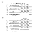
図9には、第14の実施例に係るプラズマディスプレイパネルの左上の部分に該当する6本の両側面放電電極E1乃至E6及び6本のデータ電極D1乃至D6を図示した。また、最上行から第n行目のバス電極の上側に位置する表示放電電極をEUn、下側に位置する表示放電電極をEDnと表している。例えば、第3行目の両側面放電電極E3の上側に位置する表示放電電極をEU3と表し、下側に位置する表示放電電極をED3と表している。なお、最上行の電極E1の上側には表示放電電極は不要であり、下側に位置する表示放電電極ED1のみが設けられている。そして、これらの両側面放電電極及びデータ電極に電圧を供給する駆動装置(図示せず)が設けられている。 FIG. 9 illustrates six double-sided discharge electrodes E1 to E6 and six data electrodes D1 to D6 corresponding to the upper left portion of the plasma display panel according to the fourteenth embodiment. Further, the display discharge electrode located on the upper side of the bus electrode from the top row to the nth row is represented as EUn, and the display discharge electrode located on the lower side is represented as EDn. For example, the display discharge electrode located above the both-side discharge electrodes E3 in the third row is represented as EU3, and the display discharge electrode located below is represented as ED3. Note that no display discharge electrode is required above the uppermost electrode E1, and only the display discharge electrode ED1 positioned below is provided. A driving device (not shown) for supplying a voltage to these both-side discharge electrodes and data electrodes is provided.
このように構成された第23の実施例においては、第1行目の発光表示は電極ED1と電極EU2との間の面放電に基づく発光により行われ、第2行目の表示は電極ED2と電極EU3との間の面放電に基づく発光により行われ、第3行目の表示は電極ED3と電極EU4との間の面放電に基づく発光により行われることになる。 In the twenty-third embodiment configured as described above, the light emission display in the first row is performed by light emission based on the surface discharge between the electrode ED1 and the electrode EU2, and the display in the second row is performed with the electrode ED2. The light emission based on the surface discharge between the electrode EU3 and the third row display is performed based on the light emission based on the surface discharge between the electrode ED3 and the electrode EU4.
図10は第23の実施例を駆動する方法を示すタイミングチャートである。 FIG. 10 is a timing chart showing a method of driving the 23rd embodiment.
先ず、駆動装置は、書込期間において、電極E1から順に走査パルスを垂直方向に印加し、表示データに応じて走査パルスと同期してデータ電極D1に走査パルスと逆極性のデータパルスを印加する。このとき、本実施例では、図9に示すように、バス電極の下側に配置された表示放電電極EDnの方が、上側に配置された表示放電電極EUnより低い電圧でデータ電極との間で対向放電が発生するため、適当な走査パルス電圧及びデータパルス電圧の印加により、表示放電電極EDnでのみ書込放電を発生させることができる。 First, in the writing period, the driving device applies a scan pulse in the vertical direction sequentially from the electrode E1, and applies a data pulse having a polarity opposite to that of the scan pulse to the data electrode D1 in synchronization with the scan pulse in accordance with display data. . At this time, in the present embodiment, as shown in FIG. 9, the display discharge electrode EDn disposed on the lower side of the bus electrode is connected to the data electrode at a lower voltage than the display discharge electrode EUn disposed on the upper side. Since the counter discharge is generated in this case, the write discharge can be generated only at the display discharge electrode EDn by applying an appropriate scan pulse voltage and data pulse voltage.
例えば、電極E3への走査パルス印加時に第3行目の表示データに基づいて、例えばデータ電極D2、D3及びD5にデータパルスを印加し、データ電極D1、D4、D6の電位がグランド電位にある場合は、表示放電電極ED3とデータ電極D2との間、表示放電電極ED3とデータ電極D3との間、及び表示放電電極ED3とデータ電極D5との間で対向放電が発生し、選択された表示放電電極ED3の近傍に壁電荷が生成される。このとき、同じ電圧の走査パルスが印加されているにも拘わらず、表示放電電極EU3とデータ電極D2、D3又はD5との間では対向放電が発生しないため、これらの表示セルでは表示放電電極EU3の近傍には壁電荷は生成されない。また、水平隔壁6bにより表示放電電極ED3と表示放電電極EU3とが仕切られているため、表示放電電極ED3で放電が生じても、表示放電電極EU3にまで放電が拡がることはない。
For example, when a scan pulse is applied to the electrode E3, a data pulse is applied to, for example, the data electrodes D2, D3, and D5 based on the display data in the third row, and the potentials of the data electrodes D1, D4, and D6 are at the ground potential. In this case, a counter discharge occurs between the display discharge electrode ED3 and the data electrode D2, between the display discharge electrode ED3 and the data electrode D3, and between the display discharge electrode ED3 and the data electrode D5, and the selected display Wall charges are generated in the vicinity of the discharge electrode ED3. At this time, the counter discharge does not occur between the display discharge electrode EU3 and the data electrodes D2, D3, or D5 even though the scanning pulse of the same voltage is applied. Therefore, in these display cells, the display discharge electrode EU3 No wall charge is generated in the vicinity of. Further, since the display discharge electrode ED3 and the display discharge electrode EU3 are partitioned by the
書込みが終了した後、駆動装置は、図10に示すように、各両側面放電電極に維持放電パルスを印加する。維持放電パルスは隣接する両側面放電電極間で交流パルス印加となるように印加され、面放電ギャップを挟んで隣接する表示放電電極EDnと表示放電電極EUn+1との間で面放電が発生する。この維持放電も、水平隔壁6bが存在しているため、垂直方向において隣接する表示セル間での相互間に影響は及ぼさない。同様に、垂直隔壁6aの存在及び表示放電電極が水平方向に分離されている形状のため、水平方向で隣接する表示セル間においても干渉はない。
After the addressing is completed, the driving device applies a sustain discharge pulse to each of both side surface discharge electrodes as shown in FIG. The sustain discharge pulse is applied so that an alternating pulse is applied between the adjacent side surface discharge electrodes, and a surface discharge is generated between the display discharge electrode EDn and the display discharge electrode EUn + 1 adjacent to each other with the surface discharge gap interposed therebetween. This sustain discharge also has no influence between the display cells adjacent in the vertical direction because the
このような一連の駆動をサブフィールド毎に繰り返すことにより、フルカラー表示を行うことができる。 By repeating such a series of driving for each subfield, full color display can be performed.
なお、一般に、表示を確実に行うために予備放電等の各種の準備シーケンスが採用されているが、本実施例の駆動においても準備シーケンスを採用することは有効である。また、上記の実施例では書込放電により壁電荷生成が行われるが、準備シーケンスにより予め壁電荷を生成しておき、書込放電により壁電荷を消去することにより、ネガ像の書き込みを行う消去書込み方式を用いても本願発明の効果が得られる。更に、図10に示す駆動方法には、走査ベースパルスが存在しているが、走査ベースパルスは走査ドライバに要求される耐圧を低減できること以外に、駆動マージンの拡大にも有効であり適当な電圧に設定される。 In general, various preparation sequences such as preliminary discharge are employed in order to ensure display. However, it is effective to employ the preparation sequences also in the driving of this embodiment. In the above embodiment, wall charges are generated by the write discharge. However, the wall charges are generated in advance by the preparation sequence, and the wall charges are erased by the write discharge, so that the negative image is written. Even if the writing method is used, the effect of the present invention can be obtained. Furthermore, the drive method shown in FIG. 10 has a scan base pulse. The scan base pulse can reduce the withstand voltage required for the scan driver, and is also effective for expanding the drive margin. Set to
次に、本発明の第24の実施例について説明する。第24の実施例は、駆動マージンの更なる拡大を図った駆動方法を採用したプラズマディスプレイ装置である。第23の実施例では、前述のように、走査パルスが印加されている両側面放電電極の上下に隣接する両側面放電電極には、互いに等しい電圧が印加されている。そして、0V又は図10に示したような正若しくは負の走査ベース電圧となっている。これに対して、第24の実施例では、走査パルスが印加されている両側面放電電極に隣接する一方の両側面放電電極の電圧と他方の両側面放電電極の電圧とを互いに異なるものとする。例えば、図9に示すパネル構成において、走査パルスが印加されている面放電電極の下側に隣接する両側面放電電極への印加電圧が上側に隣接する両側面放電電極への印加電圧より、走査パルスの電圧との電圧差が大きくなるように設定される。 Next, a twenty-fourth embodiment of the present invention will be described. The twenty-fourth embodiment is a plasma display device that employs a driving method in which the driving margin is further expanded. In the twenty-third embodiment, as described above, equal voltages are applied to both side discharge electrodes adjacent to the upper and lower sides of the side discharge electrodes to which the scan pulse is applied. Then, it is 0 V or a positive or negative scanning base voltage as shown in FIG. On the other hand, in the twenty-fourth embodiment, the voltage of one side discharge electrode adjacent to the side discharge electrode to which the scan pulse is applied is different from the voltage of the other side discharge electrode. . For example, in the panel configuration shown in FIG. 9, the applied voltage to the side discharge electrodes adjacent to the lower side of the surface discharge electrode to which the scan pulse is applied is scanned by the applied voltage to the side discharge electrodes adjacent to the upper side. The voltage difference from the pulse voltage is set to be large.
このように電圧を供給する場合、以下のような3相駆動の駆動波形の電圧を駆動装置により各電極に印加すればよい。図11は第24の実施例を駆動する方法を示すタイミングチャートである。 When the voltage is supplied in this way, a voltage having a driving waveform of the following three-phase driving may be applied to each electrode by the driving device. FIG. 11 is a timing chart showing a method for driving the twenty-fourth embodiment.
この駆動方法においては、両側面放電電極を両側面放電電極E1、E4、E7、E10、…の第1グループ、両側面放電電極E2、E5、E8、E11、…の第2グループ、及び両側面放電電極E3、E6、E9、E12、…の第3グループの3つのグループに分ける。 In this driving method, both side discharge electrodes are divided into a first group of both side discharge electrodes E1, E4, E7, E10,..., A second group of both side discharge electrodes E2, E5, E8, E11,. The discharge electrodes E3, E6, E9, E12,... Are divided into three groups.
第1グループの両側面放電電極E1、E4、E7、E10、…に走査パルスが印加される期間では、第2のグループには電圧Vaが印加され、第3のグループには電圧Vbが印加される。なお、走査パルスの電圧をVwとすると、電圧Vwと電圧Vaとの電圧差は、電圧Vwと電圧Vbとの電圧差より大きい。 In the period in which the scan pulse is applied to the both side surface discharge electrodes E1, E4, E7, E10,... Of the first group, the voltage Va is applied to the second group, and the voltage Vb is applied to the third group. The When the voltage of the scan pulse is Vw, the voltage difference between the voltage Vw and the voltage Va is larger than the voltage difference between the voltage Vw and the voltage Vb.
駆動装置は、第2グループの両側面放電電極E2、E5、E8、E11、…に走査パルスを印加する期間では、第1グループの両側面放電電極に電圧Vbを印加し、第3グループの両側面放電電極に電圧Vaを印加する。次の第3グループの両側面放電電極E3、E6、E9、E12、…に走査パルスを印加される期間では、第1グループの両側面放電電極に電圧Vaを印加し、第2グループ両側面放電電極に電圧Vbを印加する。 The driving device applies a voltage Vb to both side surface discharge electrodes of the first group during a period in which a scan pulse is applied to the side surface discharge electrodes E2, E5, E8, E11,. A voltage Va is applied to the surface discharge electrode. In the period in which the scan pulse is applied to the second side discharge electrodes E3, E6, E9, E12,... Of the next third group, the voltage Va is applied to the two side discharge electrodes of the first group, and the second group side discharges. A voltage Vb is applied to the electrode.
このような3相の走査では、図11に示すように、走査パルスはE1、E4、…、E2、E5、…、E3、E6、…の順に印加されるため、データ電極Djには、この走査の順番に応じたデータパルスが印加される。プラズマディスプレイ装置では、1フィールドの表示データは全てデジタルデータとして記憶されているため、このように走査の順番が変更されても、コストの増大はない。 In such a three-phase scan, as shown in FIG. 11, the scan pulses are applied in the order of E1, E4,..., E2, E5,..., E3, E6,. Data pulses corresponding to the scanning order are applied. In the plasma display device, display data for one field are all stored as digital data, so that the cost does not increase even if the scanning order is changed in this way.
例えば、電圧Vwは−190V、電圧Vaは0V、電圧Vbは走査ベース電圧と同じ−90V、データパルス電圧は60Vと設定される。このように各電圧値が設定された場合、例えば、両側面放電電極E4に−190Vの走査パネルが印加され、データ電極に60Vのデータパルスが印加された時には、表示放電電極ED4とデータ電極との間には250Vの電圧が印加され、両電極間で対向放電が発生する。このとき、両側面放電電極E5の電圧は0Vであり、対向放電をトリガとして、この対向放電とほぼ同時に、表示放電電極ED4と表示放電電極EU5との間の190Vの電圧差により、強い面放電が発生する。この放電により十分な壁電荷蓄積を伴う良好な書込み状態が実現される。 For example, the voltage Vw is set to -190V, the voltage Va is set to 0V, the voltage Vb is set to -90V which is the same as the scanning base voltage, and the data pulse voltage is set to 60V. When each voltage value is set in this way, for example, when a -190 V scanning panel is applied to the both-side discharge electrode E4 and a 60 V data pulse is applied to the data electrode, the display discharge electrode ED4 and the data electrode In between, a voltage of 250 V is applied, and a counter discharge is generated between both electrodes. At this time, the voltage on both side surface discharge electrodes E5 is 0V, and the strong surface discharge is caused by the voltage difference of 190V between the display discharge electrode ED4 and the display discharge electrode EU5 almost simultaneously with the counter discharge with the counter discharge as a trigger. Occurs. This discharge realizes a good address state with sufficient wall charge accumulation.
一方、走査パルスの印加によって表示放電電極EU4の電圧も−190Vとなっているが、データ電極及び/又は表示放電電極等の形状により対向放電開始電圧が十分高く設定されている場合には、表示放電電極EU4とデータ電極との間に対向放電は発生しない。 On the other hand, the voltage of the display discharge electrode EU4 is also -190V due to the application of the scan pulse, but when the counter discharge start voltage is set sufficiently high due to the shape of the data electrode and / or the display discharge electrode, the display is displayed. No counter discharge occurs between the discharge electrode EU4 and the data electrode.
また、対向放電開始電圧が十分高くない場合、又は何かの不具合が生じた場合には、データ放電との間で放電が発生することがあるが、このような場合においても、表示放電電極EU4と表示放電電極ED3との間の電位差は僅か100Vであるため、データ電極と表示放電電極EU4との間で不正の対向放電が発生したとしても、この放電をトリガとする面放電は発生しない。このため、少ない壁電荷しか蓄積されず書込み状態には至らない。従って、駆動マージンを広げることができる。 In addition, when the counter discharge start voltage is not sufficiently high, or when some trouble occurs, a discharge may occur between data discharges. In such a case, the display discharge electrode EU4 is also generated. And the display discharge electrode ED3 has a potential difference of only 100 V. Therefore, even if an illegal counter discharge occurs between the data electrode and the display discharge electrode EU4, a surface discharge triggered by this discharge does not occur. For this reason, only a small amount of wall charges is accumulated and the writing state is not reached. Accordingly, the drive margin can be widened.
パネル全面に書込みが終了した後、駆動装置は、図11に示すように、各両側面放電電極に維持放電パルスを印加する。維持放電パルスは隣接する両側面放電電極間で交流パルス印加となるように位相をずらして印加され、面放電ギャップを挟んで隣接する表示放電電極EDnと表示放電電極EUn−1との間で発光表示される。 After the writing is completed on the entire panel surface, the driving device applies a sustain discharge pulse to each side discharge electrode, as shown in FIG. The sustain discharge pulse is applied with a phase shift between adjacent discharge electrodes on both side surfaces, and emits light between the adjacent display discharge electrode EDn and the display discharge electrode EUn-1 across the surface discharge gap. Is displayed.
このような一連の駆動をサブフィールド毎に繰り返すことにより、フルカラー表示を行うことができる。なお、書込み動作の安定化及び高速化等のために、予備放電等の適当な準備シーケンスは本実施例においても有効である。 By repeating such a series of driving for each subfield, full color display can be performed. An appropriate preparation sequence such as preliminary discharge is also effective in this embodiment in order to stabilize and speed up the address operation.
また、このような第24の実施例における駆動方式を採用すれば、駆動マージンはやや小さくなるが、図12に示す第1の実施例のような対称パネルを駆動させることができる。図12は対称パネルを採用したプラズマディスプレイ装置を示す模式的平面図である。 Further, if such a driving method in the twenty-fourth embodiment is adopted, the driving margin is slightly reduced, but the symmetrical panel as in the first embodiment shown in FIG. 12 can be driven. FIG. 12 is a schematic plan view showing a plasma display device employing a symmetric panel.
更に、第24の実施例においては、両側面放電電極を3グループに分けているが、それ以上のグループに分けてもよい。両側面放電電極を4グループに分け4相駆動を行う第25の実施例について説明する。図13は第25の実施例を駆動する方法を示すタイミングチャートである。 Furthermore, in the twenty-fourth embodiment, the double-sided discharge electrodes are divided into three groups, but they may be divided into more groups. A twenty-fifth embodiment in which both-side discharge electrodes are divided into four groups and four-phase driving is performed will be described. FIG. 13 is a timing chart showing a method for driving the twenty-fifth embodiment.
第25の実施例においては、両側面放電電極を両側面放電電極E1、E5、E9、…の第1グループと、両側面放電電極E2、E6、E10、…の第2グループと、両側面放電電極E3、E7、E11、…の第3グループと、両側面放電電極E4、E8、E12、…の第4グループの4つのグループに分ける。 In the twenty-fifth embodiment, both side discharge electrodes are divided into a first group of both side discharge electrodes E1, E5, E9,..., A second group of both side discharge electrodes E2, E6, E10,. Are divided into four groups: a third group of electrodes E3, E7, E11,... And a fourth group of double-sided discharge electrodes E4, E8, E12,.
図9に示す構成の非対称パネルでは、駆動装置は、走査パルスを印加しているグループの下側に隣接するグループに電圧Vaを印加し、上側に隣接するグループに電圧Vbを印加する。そして、残りのグループには電圧Va、電圧Vb又は他の適当な電圧を印加する。例えば、走査パルスは−190V、電圧Vaは0V、電圧Vbは走査ベース電圧と同じ−90V、残りのグループに印加される電圧は0Vに設定される。 In the asymmetric panel having the configuration shown in FIG. 9, the driving device applies the voltage Va to the group adjacent to the lower side of the group to which the scan pulse is applied, and applies the voltage Vb to the group adjacent to the upper side. Then, the voltage Va, the voltage Vb, or other appropriate voltage is applied to the remaining groups. For example, the scan pulse is set to -190 V, the voltage Va is set to 0 V, the voltage Vb is set to -90 V, which is the same as the scan base voltage, and the voltages applied to the remaining groups are set to 0 V.
このように構成された第25の実施例においても、書込終了後、隣接する両側面放電電極間に交流の維持パルスが印加され、発光表示される。 Also in the twenty-fifth embodiment configured as described above, an alternating sustain pulse is applied between the adjacent discharge electrodes on both sides after the writing is completed, and light emission is displayed.
3グループの駆動を採用した第24の実施例では、同じグループの面放電電極に印加される維持パルスの位相として2種類の位相が必要である。例えば、同じ第1グループに属する両側面放電電極E1及びE4では、維持パルスの位相が異なっており、別々の維持パルス発生回路に接続する必要がある。このため、維持パルス発生回路の構成が複雑になる。 In the twenty-fourth embodiment employing three groups of driving, two types of phases are necessary as the phases of the sustain pulses applied to the surface discharge electrodes of the same group. For example, the side discharge electrodes E1 and E4 belonging to the same first group have different sustain pulse phases and need to be connected to separate sustain pulse generation circuits. This complicates the configuration of the sustain pulse generation circuit.
これに対して、4グループの駆動を採用した第25の実施例では、同じグループの両側面放電電極には同じ位相の維持パルスが印加されるため、回路構成が簡略化できる利点がある。 On the other hand, in the twenty-fifth embodiment adopting four groups of driving, the sustain pulses having the same phase are applied to the both-side discharge electrodes of the same group, so that there is an advantage that the circuit configuration can be simplified.
更に多くのグループに分けることもできるが、それによる特段の効果はなく、4グループまでの分割で十分である。なお、この第25の実施例における駆動方法は第24の実施例と同様、対称パネルにも適用可能である。 Although it can be divided into more groups, there is no particular effect, and a division of up to four groups is sufficient. The driving method in the twenty-fifth embodiment can be applied to a symmetric panel as in the twenty-fourth embodiment.
次に、本発明の第26の実施例について説明する。図14は第26の実施例を駆動する方法を示すタイミングチャートである。第24の実施例においては、駆動装置は、電圧Vwの走査パルスを走査期間に両側面放電電極E1、E2、E3、…の順に印加するが、走査パルスを印加するまでの期間に両側面放電電極に印加する電圧は電圧Vaであり、走査パルスを印加した後に両側面放電電極に印加する電圧は電圧Vbである。なお、電圧Vwと電圧Vaとの電圧差の方が電圧Vwと電圧Vbとの電圧差より大きい。 Next, a twenty-sixth embodiment of the present invention is described. FIG. 14 is a timing chart showing a method for driving the twenty-sixth embodiment. In the twenty-fourth embodiment, the driving device applies the scan pulse of the voltage Vw in the order of the double-sided discharge electrodes E1, E2, E3,... During the scan period, but the double-sided discharge during the period until the scan pulse is applied. The voltage applied to the electrodes is the voltage Va, and the voltage applied to the both-side discharge electrodes after applying the scan pulse is the voltage Vb. Note that the voltage difference between the voltage Vw and the voltage Va is larger than the voltage difference between the voltage Vw and the voltage Vb.
このような駆動方法を採用する第26の実施例においては、駆動装置は、走査パルスを印加している両側面放電電極Enの上側に隣接する両側面放電電極En−1に電圧Vbを印加し、下側に隣接する両側面放電電極En+1に電圧Vaを印加する。例えば、両側面放電電極E3に走査パルスを印加している時には、両側面放電電極E2に電圧Vbを印加し、両側面放電電極E4に電圧Vaを印加する。 In the twenty-sixth embodiment employing such a driving method, the driving device applies the voltage Vb to the side discharge electrode En-1 adjacent to the upper side of the side discharge electrode En applying the scan pulse. Then, a voltage Va is applied to both side discharge electrodes En + 1 adjacent to the lower side. For example, when a scanning pulse is applied to the both-side discharge electrode E3, the voltage Vb is applied to the both-side discharge electrode E2, and the voltage Va is applied to the both-side discharge electrode E4.
例えば、走査パルスが−190V、電圧Vaが0V、電圧Vbが−90Vに設定された場合、両側面放電電極E3に走査パルスが印加されている時には、表示放電電極ED3と表示放電電極EU4との間には190Vもの印加電圧差があるが、表示放電電極EU3と表示放電電極ED2との間には100Vの印加電圧差しかない。従って、表示放電電極ED3とデータ電極との間で対向放電が発生し、これをトリガとして表示放電電極ED3と表示放電電極EU4との間に面放電が発生し、良好な書込み状態が実現される。一方、表示放電電極EU3とデータ電極との間で対向放電が発生した場合でも、表示放電電極EU3と表示放電電極ED2との間ではこれをトリガとする面放電が発生しない。このため、書込み状態とはならない。 For example, when the scan pulse is set to -190 V, the voltage Va is set to 0 V, and the voltage Vb is set to -90 V, when the scan pulse is applied to the both-side discharge electrodes E3, the display discharge electrode ED3 and the display discharge electrode EU4 There is an applied voltage difference of 190V between them, but there is only an applied voltage difference of 100V between the display discharge electrode EU3 and the display discharge electrode ED2. Accordingly, a counter discharge is generated between the display discharge electrode ED3 and the data electrode, and this is used as a trigger to generate a surface discharge between the display discharge electrode ED3 and the display discharge electrode EU4, thereby realizing a good address state. . On the other hand, even when a counter discharge is generated between the display discharge electrode EU3 and the data electrode, no surface discharge is triggered between the display discharge electrode EU3 and the display discharge electrode ED2. For this reason, the writing state is not achieved.
全ての書込み動作を完了した後、駆動回路が各電極に維持パルスを印加することにより、発光表示が行われる。この動作をサブフィールド毎に繰り返すことによりフルカラー表示される。なお、準備シーケンスの採用により、より確実な動作ができることは前述の実施例と同様である。また、第26の実施例においても、非対称パネルの方が駆動マージンを確保するためにより好ましいが、第24及び第25の実施例と同様、対称パネルを使用することもできる。 After all the writing operations are completed, the drive circuit applies a sustain pulse to each electrode, whereby light emission display is performed. By repeating this operation for each subfield, full color display is performed. In addition, it is the same as that of the above-mentioned Example that operation | movement more reliably is employable by adoption of a preparation sequence. Also in the twenty-sixth embodiment, the asymmetric panel is more preferable in order to secure a drive margin. However, as in the twenty-fourth and twenty-fifth embodiments, a symmetric panel can be used.
次に、本発明の第27の実施例について説明する。第27の実施例は、インターレース表示を適用したプラズマディスプレイ装置である。図15は第27の実施例を駆動する方法を示す図であって、(a)は奇数フィールドの駆動波形を示すタイミングチャート、(b)は偶数フィールドの駆動波形を示すタイミングチャートである。 Next, a twenty-seventh embodiment of the present invention is described. The twenty-seventh embodiment is a plasma display device to which interlaced display is applied. FIGS. 15A and 15B are diagrams showing a method of driving the twenty-seventh embodiment. FIG. 15A is a timing chart showing driving waveforms in odd fields, and FIG. 15B is a timing chart showing driving waveforms in even fields.
奇数フィールドの表示では、駆動装置は両側面放電電極E1から1本置きに走査パルスを印加する。このようにして奇数番目の両側面放電電極が走査されている間は、偶数番目の両側面放電電極の電圧は適当な電圧Vaに固定されている。例えば、走査パルスの電圧Vwは−190V、走査ベース電圧は−90V、電圧Vaは0Vに設定される。 In the odd-field display, the driving device applies a scanning pulse every other one from both side discharge electrodes E1. In this manner, while the odd-numbered both-side discharge electrodes are scanned, the voltage of the even-numbered both-side discharge electrodes is fixed to an appropriate voltage Va. For example, the scan pulse voltage Vw is set to -190V, the scan base voltage is set to -90V, and the voltage Va is set to 0V.
このような駆動方法を採用した第27の実施例においては、例えば、両側面放電電極E3に走査パルスが印加された際には、図9に示した非対称パネルの場合では、表示放電電極ED3とデータ電極との間で対向放電が発生する。そして、この対向放電をトリガとして表示放電電極ED3と表示放電電極EU4との間で面放電が発生し、良好な書込み状態となる。一方、表示放電電極EU3とデータ電極との間では対向放電が発生しないため、書込み状態とはならない。 In the twenty-seventh embodiment adopting such a driving method, for example, when a scan pulse is applied to the discharge electrodes E3 on both sides, in the case of the asymmetric panel shown in FIG. A counter discharge is generated between the data electrodes. Then, using this counter discharge as a trigger, a surface discharge is generated between the display discharge electrode ED3 and the display discharge electrode EU4, and a good address state is obtained. On the other hand, since no counter discharge occurs between the display discharge electrode EU3 and the data electrode, the address state is not achieved.
このようにして奇数行の表示セルの書込みが行われた後、駆動装置は維持パルスを印加する。維持パルスとしては、奇数番目の表示行の表示セルを構成する表示放電電極間に交流パルスが印加され、偶数番目の表示行の表示セルには実効的に維持パルスが印加されないように、各両側面放電電極に印加される維持パルスの位相が設定されている。即ち、図15(a)に示すように、両側面放電電極が、両側面放電電極E1、E4、E5、E8、E9、…の第1グループ及び両側面放電電極E2、E3、E6、E7、E10、E11、…の第2グループに分けられ、グループ内では同相、グループ間では位相をずらしたタイミングで維持パルスが印加される。このような維持パルスの印加により、奇数行の表示セルのみが表示発光される。 After the display cells in the odd-numbered rows are thus written, the driving device applies a sustain pulse. As the sustain pulse, an AC pulse is applied between the display discharge electrodes constituting the display cells of the odd-numbered display rows, and the sustain pulses are not effectively applied to the display cells of the even-numbered display rows. The phase of the sustain pulse applied to the surface discharge electrode is set. That is, as shown in FIG. 15 (a), both side discharge electrodes are divided into a first group of both side discharge electrodes E1, E4, E5, E8, E9,... And both side discharge electrodes E2, E3, E6, E7, The sustain pulses are applied to the second group of E10, E11,..., And are in-phase within the group and shifted in phase between the groups. By applying such a sustain pulse, only odd-numbered display cells display light.
次に、図15(b)に示すように、駆動装置は偶数番目の両側面放電電極E2、E4、…に走査パルスを印加する。このとき、奇数番目の両側面放電電極は0Vである。書込みが終了した後、駆動装置は偶数番目の表示行の表示セルを構成する表示放電電極に交流パルスが印加されるように維持パルスを印加する。即ち、両側面放電電極が、両側面放電電極E1、E2、E5、E6、…の第3グループ及び両側面放電電極E3、E4、E7、E8、…の第4グループの2つのグループに分けられ、グループ内では同相、グループ間では異相となるように維持パルスが印加される。これにより、偶数行の表示セルのみが表示発光される。 Next, as shown in FIG. 15B, the driving device applies a scan pulse to the even-numbered side-surface discharge electrodes E2, E4,. At this time, the odd-numbered both-side discharge electrodes are at 0V. After the writing is completed, the driving device applies a sustain pulse so that an AC pulse is applied to the display discharge electrodes constituting the display cells of the even-numbered display rows. That is, the double-sided discharge electrodes are divided into two groups, a third group of double-sided discharge electrodes E1, E2, E5, E6,... And a fourth group of double-sided discharge electrodes E3, E4, E7, E8,. The sustain pulse is applied so as to be in-phase within the group and different in phase between the groups. As a result, only the display cells in even-numbered rows emit display light.
従って、奇数行の表示と偶数行の表示が分離されたインターレースの表示となるが、高速で繰り返されるために視覚上の問題は生じない。なお、フルカラー表示を行うためには、複数のサブフィールド表示を行う必要があるが、各サブフィールド毎に奇数行及び偶数行の表示を行ってもよく、奇数行の全てのサブフィールド表示を完了した後に偶数行の全てのサブフィールド表示を行ってもよい。また、これらを混合して行ってもよい。 Therefore, although the display of odd lines and the display of even lines are separated, the display is interlaced. However, since the display is repeated at high speed, there is no visual problem. In order to perform full color display, it is necessary to display a plurality of subfields. However, display of odd and even lines may be performed for each subfield, and all subfield displays of odd lines are completed. After that, all the subfields in even lines may be displayed. Moreover, you may carry out by mixing these.
第27の実施例によれば、例えば、正常動作ではバス電極の下側の表示放電電極のみで書込みがなされるが、何らかの不具合によりバス電極の上側の表示放電電極でもデータ電極と不正の書込み放電が発生し、更に面放電が発生し強い書込み状態に至った場合においても、この表示セルでは、2個の表示放電電極に印加されている維持パルスが互いに同相であるため、維持放電は発生しない。従って、誤点灯表示になることはない。 According to the twenty-seventh embodiment, for example, in normal operation, the address is written only by the display discharge electrode on the lower side of the bus electrode. In this display cell, since the sustain pulses applied to the two display discharge electrodes are in phase with each other, no sustain discharge occurs even when surface discharge occurs and a strong address state is reached. . Therefore, there is no false lighting display.
このため、第27の実施例を、図12に示すような対称パネルに適用しても、誤点灯を防止することができる。例えば、奇数フィールドで両側面放電電極E3に走査パルスが印加された場合には、データ電極と表示放電電極ED3との間だけではなく、データ電極と表示放電電極EU3との間にも対向放電が発生し、これをトリガとした面放電電極も発生するため、表示放電電極ED3も表示放電電極EU3も書込み状態となる。しかし、維持パルスの位相の関係により、表示放電電極ED3と表示放電電極EU4との間では維持放電が発生するが、表示放電電極EU3と表示放電電極ED2との間では維持放電は発生しない。 For this reason, even if the twenty-seventh embodiment is applied to a symmetrical panel as shown in FIG. 12, erroneous lighting can be prevented. For example, when a scan pulse is applied to the discharge electrodes E3 on both sides in an odd field, not only the data electrode and the display discharge electrode ED3 but also the counter discharge is generated between the data electrode and the display discharge electrode EU3. Since this occurs and a surface discharge electrode triggered by this is also generated, both the display discharge electrode ED3 and the display discharge electrode EU3 are in an address state. However, the sustain discharge occurs between the display discharge electrode ED3 and the display discharge electrode EU4 due to the phase relationship of the sustain pulse, but no sustain discharge occurs between the display discharge electrode EU3 and the display discharge electrode ED2.
このため、対称パネルに適用しても、正常な表示が実現される。但し、非対称パネルの方が、不要な書込み放電がないため、走査ドライバの電流供給能力が低くてもよく、より好ましい。 For this reason, even when applied to a symmetric panel, normal display is realized. However, the asymmetric panel is more preferable because there is no unnecessary address discharge and the current supply capability of the scan driver may be low.
第27の実施例では、走査に要する時間は従来のものと同等であるが、維持発光が奇数行と偶数行とで別々に行われるため、維持期間が増加するものの、広い動作マージンが得られること、対称パルスが使用できること及び維持放電電力が分散されること等の効果が得られる。 In the twenty-seventh embodiment, the time required for scanning is the same as that of the conventional one, but since sustain light emission is performed separately for odd and even rows, the sustain period increases, but a wide operating margin is obtained. In addition, effects such as the use of symmetric pulses and the dispersion of sustain discharge power can be obtained.
次に、インターレース駆動を利用して走査ドライバの半減を図った第28の実施例について説明する。第28の実施例は、図12に示す対称パネルに適用される。図16は第28の実施例を駆動する方法を示す図であって、(a)は奇数フィールドの駆動波形を示すタイミングチャート、(b)は偶数フィールドの駆動波形を示すタイミングチャートである。 Next, a twenty-eighth embodiment in which the number of scanning drivers is reduced by utilizing interlaced driving will be described. The twenty-eighth embodiment is applied to the symmetric panel shown in FIG. FIGS. 16A and 16B are diagrams showing a method of driving the twenty-eighth embodiment, wherein FIG. 16A is a timing chart showing driving waveforms in odd fields, and FIG. 16B is a timing chart showing driving waveforms in even fields.
図16(a)に示すように、例えば両側面放電電極E2が走査された場合では、1行目の表示データにより表示放電電極EU2以外に、2行目の表示セル内にある表示放電電極ED2でも書込みが行われる。しかし、その後引き続き印加される維持パルスにより、奇数行目の表示セルだけが維持発光される。 As shown in FIG. 16A, for example, when the both-side discharge electrodes E2 are scanned, the display discharge electrodes ED2 in the display cells in the second row are displayed in addition to the display discharge electrodes EU2 by the display data in the first row. But writing is done. However, only the odd-numbered display cells emit sustain light by the sustain pulse subsequently applied.
次の偶数フィールドの表示においては、駆動装置は、奇数フィールドの表示と同様、走査パルスを偶数番目の両側面放電電極に印加する。但し、走査パルスとデータパルスとのタイミングに関し、奇数フィールドの表示では、例えば両側面放電電極E2に走査パルスが印加された際には1行目の表示データに基づいてデータ電極にデータパルスを印加するが、偶数フィールドの表示では、両側面放電電極E2には2行目の表示データに基づいてデータ電極にデータパルスを印加する。従って、この走査においても、表示放電電極EU2及びED2の両方の表示放電電極でデータ電極との間の対向放電及びこれをトリガとする面放電が発生し、書き込み状態になる。しかし、図16(b)に示すように、偶数番目の行の表示セルに対してのみ交流の維持パルスが印加されるため、例えば、表示放電電極ED2と表示放電電極EU3との間で維持放電が発生するのに対し、表示放電電極EU2と表示放電電極ED1との間では維持放電は発生しない。 In the display of the next even field, the driving device applies the scan pulse to the even-numbered side discharge electrodes as in the display of the odd field. However, regarding the timing of the scan pulse and the data pulse, in the display of the odd field, for example, when the scan pulse is applied to the both-side discharge electrode E2, the data pulse is applied to the data electrode based on the display data of the first row. However, in the display of the even field, a data pulse is applied to the data electrode based on the display data of the second row on the both side discharge electrodes E2. Therefore, also in this scanning, both the display discharge electrodes EU2 and ED2 generate a counter discharge between the display discharge electrodes EU2 and ED2 and a surface discharge triggered by the data discharge, resulting in a writing state. However, as shown in FIG. 16B, since the sustain pulse of alternating current is applied only to the display cells in the even-numbered rows, for example, the sustain discharge is generated between the display discharge electrode ED2 and the display discharge electrode EU3. However, no sustain discharge occurs between the display discharge electrode EU2 and the display discharge electrode ED1.
この結果、奇数フィールドの表示では、バス電極の上側の表示放電電極への書込みが維持放電発光に有効であり、偶数フィールドの表示では、バス電極の下側の表示放電電極への書込みが維持放電発光に有効になる。 As a result, in the odd field display, writing to the display discharge electrode above the bus electrode is effective for sustain discharge light emission, and in the even field display, writing to the display discharge electrode below the bus electrode is sustain discharge. Effective for light emission.
このような駆動方法によれば、偶数番目の両側面放電電極にのみ走査パルスを印加するだけで、パネル全面の表示を行うことができるので、走査ドライバ数を半減することができ、低コスト化に寄与する。また、準備シーケンスの採用並びに奇数フィールドの表示、偶数フィールドの表示及びサブフィールド表示の組合せは、第27の実施例と同様に、任意に行うことができる。 According to such a driving method, it is possible to display the entire surface of the panel only by applying a scanning pulse only to the even-numbered both-side discharge electrodes, thereby reducing the number of scanning drivers by half and reducing the cost. Contribute to. Further, the adoption of the preparation sequence and the combination of the odd field display, the even field display, and the subfield display can be arbitrarily performed as in the twenty-seventh embodiment.
また、本実施例では偶数番目の両側面放電電極に走査ドライバを接続する構造を採用しているが、維持パルスの位相関係を整合させることにより、奇数番目の面放電電極に走査ドライバを接続してもよい。但し、表示行は偶数行であることが一般的であり、この場合、偶数行に走査ドライバを接続する構成とする方が、1ビット分少なくすることができるので、より好ましい。 In this embodiment, the scan driver is connected to the even-numbered side discharge electrodes. However, the scan driver is connected to the odd-numbered surface discharge electrodes by matching the phase relationship of the sustain pulses. May be. However, it is general that the display rows are even rows. In this case, it is more preferable to connect the scan driver to the even rows because one bit can be reduced.
次に、隣接する2表示行を同じ表示として発光表示させる第29の実施例について説明する。第29の実施例は、両側面放電電極を有する対称パネルに適用される。図17は第29の実施例を駆動する方法を示す図であって、(a)は奇数フィールドの駆動波形を示すタイミングチャート、(b)は偶数フィールドの駆動波形を示すタイミングチャートである。 Next, a description will be given of a twenty-ninth embodiment in which two adjacent display lines are lit and displayed as the same display. The twenty-ninth embodiment is applied to a symmetric panel having double-sided discharge electrodes. FIGS. 17A and 17B are diagrams showing a method of driving the twenty-ninth embodiment, wherein FIG. 17A is a timing chart showing driving waveforms in odd fields, and FIG. 17B is a timing chart showing driving waveforms in even fields.
第29の実施例においては、図17(a)に示すように、奇数フィールドの表示では、駆動装置は奇数番目の両側面放電電極に走査パルスを印加する。本実施例では、対称パネルが使用されるので、例えば、両側面放電電極E3に走査パルスが印加されるタイミングでデータ電極にデータパルスが印加されると、表示放電電極ED3及びEU3の両方が書込み状態となる。そして、このような奇数番目の両側面放電電極に対する走査がパネル全体に行われた後、図17(a)に示すように、駆動装置は隣接する両側面放電電極間に交流の維持パルスを印加する。この際、奇数番目の両側面放電電極の両側の表示放電電極に書込みが行われているため、2表示行が同じ発光表示状態で維持発光する。 In the twenty-ninth embodiment, as shown in FIG. 17A, in the odd field display, the driving device applies a scan pulse to the odd-numbered both-side discharge electrodes. In this embodiment, since a symmetric panel is used, for example, when a data pulse is applied to the data electrode at the timing when the scanning pulse is applied to the both-side discharge electrode E3, both the display discharge electrodes ED3 and EU3 are written. It becomes a state. Then, after scanning the odd-numbered both-side discharge electrodes on the entire panel, as shown in FIG. 17A, the driving device applies an AC sustain pulse between the adjacent both-side discharge electrodes. To do. At this time, since writing is performed on the display discharge electrodes on both sides of the odd-numbered both-side discharge electrodes, the two display rows emit sustain light in the same light emission display state.
次いで、図17(b)に示すように、偶数フィールドの表示において、駆動装置は偶数番目の両側面放電電極に走査パルスを印加して、その両側の表示放電電極に書込みを行い、その後、維持パルスを印加する。維持パルスは隣接する両側面放電電極間に交流の維持パルスとして印加されるため、2表示行が同じ発光表示状態で維持発光する。 Next, as shown in FIG. 17B, in the even-field display, the driving device applies a scan pulse to the even-numbered both-side discharge electrodes, writes the display discharge electrodes on both sides, and then maintains the scan pulses. Apply a pulse. Since the sustain pulse is applied as an alternating sustain pulse between the adjacent discharge electrodes on both sides, the two display rows emit sustain light in the same light emission display state.
このような表示方法は、交互2行走査型のインターレース表示方法に相当するため、解像度はやや低下するが、維持発光が半分の行でのみ行われる第23及び24の実施例とは異なり、維持発光がパネルの全ての行で行われるため、高輝度発光が実現される。 Since such a display method corresponds to an alternate two-row scanning interlaced display method, the resolution is slightly lowered, but unlike the twenty-third and twenty-fourth embodiments in which the sustain light emission is performed only in half the rows, the sustain is maintained. Since light emission is performed in all the rows of the panel, high luminance light emission is realized.
また、インターレースの発光表示が互いに重なっているため、例えば、従来のテレビと同じ1フレームを30分の1秒でインタレース表示を行っても、フリッカ及び走査線構造の妨害は抑制される。この場合、通常の60分の1秒の順次走査走査と比較して、走査時間及び維持発光時間に余裕があり、高輝度化及び低コスト化に寄与できる。 Further, since the interlaced light emitting displays overlap each other, for example, even if the same frame as the conventional television is displayed in 1/30 second, flicker and scanning line structure interference are suppressed. In this case, compared with a normal 1/60 second sequential scanning scan, there is a margin in scanning time and sustain light emission time, which can contribute to higher luminance and lower cost.
従って、第29の実施例においては、インターレースでビデオデータが送られるテレビジョン表示との親和性が高い。また、高輝度及び高解像度表示が実現されるため、テレビジョン表示では第25の実施例における交互2行走査型の駆動方法を採用し、パーソナルコンピュータ等の表示を行う場合に駆動方法を第22乃至26の実施例のいずれかにおける駆動方法に自動的に切換えれば、高解像度でラインフリッカのない鮮明な表示を行うこともできる。 Accordingly, in the twenty-ninth embodiment, the compatibility with a television display in which video data is transmitted in an interlaced manner is high. Further, since a high luminance and high resolution display is realized, the alternate two-row scanning type driving method in the twenty-fifth embodiment is adopted for television display, and the driving method is used when displaying on a personal computer or the like. If the driving method is automatically switched to any one of the thirty-sixth embodiments, a clear display with high resolution and no line flicker can be performed.
これらの実施例に係るプラズマディスプレイ装置には、全ての両側面放電電極に走査ドライバ(駆動装置)が接続されるもの、その半数に走査ドライバが接続されるものがあり、また、多相に分けて走査パルスが印加されるものもあるが、いずれの場合にも、パネルからの両側面放電電極端子は交互に左右に取り出し、駆動装置に接続されていることが望ましい。これは、維持発光強度の左右の分布をなくするためである。厳密には、維持パルスを供給する外部駆動回路と交互に左右から接続すればよいが、走査ドライバICの出力端子を通じて維持パルスも供給されるため、全ての電極に走査ドライバが接続されるこれらの実施例においても、交互に左右取り出しとし、駆動装置に接続されていることが望ましい。 Some of the plasma display devices according to these embodiments have a scanning driver (driving device) connected to all the discharge electrodes on both sides, and half of them have a scanning driver connected, and are divided into multiple phases. In either case, it is desirable that the discharge electrode terminals on both side surfaces from the panel are alternately taken to the left and right and connected to the driving device. This is to eliminate the left and right distribution of the sustain emission intensity. Strictly speaking, the external drive circuit that supplies the sustain pulse may be connected alternately from the left and right, but since the sustain pulse is also supplied through the output terminal of the scan driver IC, the scan driver is connected to all the electrodes. Also in the embodiment, it is desirable to alternately take out the left and right, and to connect to the driving device.
なお、本発明のプラズマディスプレイパネルでは、データ電極を上下で分離して、パネル2分割走査を行う構造にも同様に有効であり、デュアル走査により表示容量の増大及びデータパルス印加電力の低減を図ることができることは従来のプラズマディスプレイパネルと同様である。 Note that the plasma display panel of the present invention is also effective for a structure in which the data electrodes are separated into upper and lower parts and the panel is divided into two parts, and the display capacity is increased and the data pulse application power is reduced by dual scanning. This is possible in the same manner as a conventional plasma display panel.
なお、図示した各実施例の駆動波形の例は、説明を分かりやすくするため、比較的単純な波形となっているが、交流駆動のプラズマディスプレイでは相対的な電位が重要であり、また壁電荷によるバイアス効果を利用できるため、準備シーケンスも含めて、適当なバイアスを利用した波形設計を行うことができる。このような場合、図示した実施例で説明した波形とは異なる波形の設計も容易に行うことができるが、前述の実施例における要旨と同様のものであれば、本発明の効果が得られる。 In addition, although the example of the drive waveform of each Example shown in figure is a comparatively simple waveform in order to make explanation easy to understand, in an AC drive plasma display, a relative electric potential is important, and wall charge Therefore, it is possible to design a waveform using an appropriate bias including a preparation sequence. In such a case, it is possible to easily design a waveform different from the waveform described in the illustrated embodiment, but the effect of the present invention can be obtained if it is the same as the gist of the above-described embodiment.
また、各実施例の説明では、奇数番目、偶数番目、上側、下側、垂直、水平、奇数フィールド及び偶数フィールド等の部材を特定する記載があるが、これらは説明を分かりやすくするためのものである。即ち、これらは厳密な規定ではなく、これらに限定されるものではない。また、非対称パネルの場合では、書込み放電電圧が低い表示放電電極の配置に駆動波形を整合させればよいので、プラズマディスプレイ装置の構成は、図9に示すものに限定されず、他の実施例に係るプラズマディスプレイパネルが組み込んまれたものとすることができる。 Further, in the description of each embodiment, there is a description for specifying members such as odd-numbered, even-numbered, upper side, lower side, vertical, horizontal, odd-numbered field and even-numbered field, but these are for easy understanding. It is. That is, these are not strict regulations and are not limited to these. In the case of an asymmetric panel, the driving waveform may be matched to the arrangement of the display discharge electrodes having a low address discharge voltage, so the configuration of the plasma display device is not limited to that shown in FIG. The plasma display panel according to the above can be incorporated.
1、2;ガラス基板
2a;突出部
3、3−2、3−3、3−4a、3−6、3−7、3−8、3−9;透明電極膜
3−4b;金属パタン
4、4−20;バス電極
5、5−13、5−14、5−15、5−16、5−19;データ電極
6a、6b、6a−22、6b−22;隔壁
7、7−11、7−12;誘電体層
8、8−2、8−3、8−4、8−5、8−6a、8−6b、8−7a、8−7b、8−8a、8−8b、8−9a、8−9b、8−11;表示放電電極
10、10−17、10−18a、10−18b;誘電体層
10−17a;窪み
20;盛り上げ部
100;前面基板
200;背面基板
300;両側面放電電極
1, 2; Glass substrate 2a;
Claims (10)
Priority Applications (1)
| Application Number | Priority Date | Filing Date | Title |
|---|---|---|---|
| JP2004132809A JP4208761B2 (en) | 2004-04-28 | 2004-04-28 | Plasma display device |
Applications Claiming Priority (1)
| Application Number | Priority Date | Filing Date | Title |
|---|---|---|---|
| JP2004132809A JP4208761B2 (en) | 2004-04-28 | 2004-04-28 | Plasma display device |
Related Parent Applications (1)
| Application Number | Title | Priority Date | Filing Date |
|---|---|---|---|
| JP36561999A Division JP3933831B2 (en) | 1999-12-22 | 1999-12-22 | Plasma display device |
Related Child Applications (1)
| Application Number | Title | Priority Date | Filing Date |
|---|---|---|---|
| JP2007026195A Division JP2007183657A (en) | 2007-02-05 | 2007-02-05 | Plasma display device |
Publications (2)
| Publication Number | Publication Date |
|---|---|
| JP2004252484A JP2004252484A (en) | 2004-09-09 |
| JP4208761B2 true JP4208761B2 (en) | 2009-01-14 |
Family
ID=33028643
Family Applications (1)
| Application Number | Title | Priority Date | Filing Date |
|---|---|---|---|
| JP2004132809A Expired - Fee Related JP4208761B2 (en) | 2004-04-28 | 2004-04-28 | Plasma display device |
Country Status (1)
| Country | Link |
|---|---|
| JP (1) | JP4208761B2 (en) |
-
2004
- 2004-04-28 JP JP2004132809A patent/JP4208761B2/en not_active Expired - Fee Related
Also Published As
| Publication number | Publication date |
|---|---|
| JP2004252484A (en) | 2004-09-09 |
Similar Documents
| Publication | Publication Date | Title |
|---|---|---|
| JP3933831B2 (en) | Plasma display device | |
| US5661500A (en) | Full color surface discharge type plasma display device | |
| US6531819B1 (en) | Surface discharge plasma display panel | |
| US7589697B1 (en) | Addressing of AC plasma display | |
| US6603263B1 (en) | AC plasma display panel, plasma display device and method of driving AC plasma display panel | |
| US20020063664A1 (en) | Full color surface discharge type plasma display device | |
| JP2000123748A (en) | Color plasma display panel | |
| JP3641240B2 (en) | Plasma display panel and driving method thereof | |
| US6603266B1 (en) | Flat-panel display | |
| JP3309818B2 (en) | Plasma display panel and display method thereof | |
| JP3688142B2 (en) | Plasma display panel | |
| EP1347488A1 (en) | Plasma display device | |
| JP2002215082A (en) | Image display panel and driving method therefor | |
| JP3449252B2 (en) | Plasma display panel, method of manufacturing the same, and display device using the same | |
| JP4208761B2 (en) | Plasma display device | |
| JPH11329252A (en) | Plasma display device and drive method for plasma display panel | |
| JP2007183657A (en) | Plasma display device | |
| US20070018913A1 (en) | Plasma display panel, plasma display device and driving method therefor | |
| JP3994626B2 (en) | Plasma display panel | |
| KR100226166B1 (en) | Ac type plasma display panel | |
| KR20020050817A (en) | Plasma display panel | |
| JP4359997B2 (en) | AC type plasma display panel | |
| JP4108044B2 (en) | AC type plasma display panel | |
| KR100421490B1 (en) | Plasma Display Panel With 3 Electrodes of Trigger-Sustainning Electrode Structure | |
| KR20030037293A (en) | Plasma display panel |
Legal Events
| Date | Code | Title | Description |
|---|---|---|---|
| A711 | Notification of change in applicant |
Free format text: JAPANESE INTERMEDIATE CODE: A711 Effective date: 20041019 |
|
| RD01 | Notification of change of attorney |
Free format text: JAPANESE INTERMEDIATE CODE: A7421 Effective date: 20050107 |
|
| RD01 | Notification of change of attorney |
Free format text: JAPANESE INTERMEDIATE CODE: A7421 Effective date: 20050428 |
|
| A711 | Notification of change in applicant |
Free format text: JAPANESE INTERMEDIATE CODE: A711 Effective date: 20050328 |
|
| A131 | Notification of reasons for refusal |
Free format text: JAPANESE INTERMEDIATE CODE: A131 Effective date: 20061205 |
|
| A521 | Written amendment |
Free format text: JAPANESE INTERMEDIATE CODE: A523 Effective date: 20070205 |
|
| A131 | Notification of reasons for refusal |
Free format text: JAPANESE INTERMEDIATE CODE: A131 Effective date: 20070515 |
|
| A521 | Written amendment |
Free format text: JAPANESE INTERMEDIATE CODE: A523 Effective date: 20070717 |
|
| A521 | Written amendment |
Free format text: JAPANESE INTERMEDIATE CODE: A523 Effective date: 20070718 |
|
| A131 | Notification of reasons for refusal |
Free format text: JAPANESE INTERMEDIATE CODE: A131 Effective date: 20080708 |
|
| A521 | Written amendment |
Free format text: JAPANESE INTERMEDIATE CODE: A523 Effective date: 20080908 |
|
| TRDD | Decision of grant or rejection written | ||
| A01 | Written decision to grant a patent or to grant a registration (utility model) |
Free format text: JAPANESE INTERMEDIATE CODE: A01 Effective date: 20081021 |
|
| A01 | Written decision to grant a patent or to grant a registration (utility model) |
Free format text: JAPANESE INTERMEDIATE CODE: A01 |
|
| A61 | First payment of annual fees (during grant procedure) |
Free format text: JAPANESE INTERMEDIATE CODE: A61 Effective date: 20081021 |
|
| R150 | Certificate of patent or registration of utility model |
Free format text: JAPANESE INTERMEDIATE CODE: R150 |
|
| FPAY | Renewal fee payment (event date is renewal date of database) |
Free format text: PAYMENT UNTIL: 20111031 Year of fee payment: 3 |
|
| FPAY | Renewal fee payment (event date is renewal date of database) |
Free format text: PAYMENT UNTIL: 20111031 Year of fee payment: 3 |
|
| S111 | Request for change of ownership or part of ownership |
Free format text: JAPANESE INTERMEDIATE CODE: R313113 |
|
| FPAY | Renewal fee payment (event date is renewal date of database) |
Free format text: PAYMENT UNTIL: 20111031 Year of fee payment: 3 |
|
| R360 | Written notification for declining of transfer of rights |
Free format text: JAPANESE INTERMEDIATE CODE: R360 |
|
| FPAY | Renewal fee payment (event date is renewal date of database) |
Free format text: PAYMENT UNTIL: 20111031 Year of fee payment: 3 |
|
| R370 | Written measure of declining of transfer procedure |
Free format text: JAPANESE INTERMEDIATE CODE: R370 |
|
| FPAY | Renewal fee payment (event date is renewal date of database) |
Free format text: PAYMENT UNTIL: 20111031 Year of fee payment: 3 |
|
| S111 | Request for change of ownership or part of ownership |
Free format text: JAPANESE INTERMEDIATE CODE: R313113 |
|
| FPAY | Renewal fee payment (event date is renewal date of database) |
Free format text: PAYMENT UNTIL: 20111031 Year of fee payment: 3 |
|
| R350 | Written notification of registration of transfer |
Free format text: JAPANESE INTERMEDIATE CODE: R350 |
|
| FPAY | Renewal fee payment (event date is renewal date of database) |
Free format text: PAYMENT UNTIL: 20121031 Year of fee payment: 4 |
|
| FPAY | Renewal fee payment (event date is renewal date of database) |
Free format text: PAYMENT UNTIL: 20131031 Year of fee payment: 5 |
|
| LAPS | Cancellation because of no payment of annual fees |