JP4201248B2 - Electrical junction box - Google Patents
Electrical junction box Download PDFInfo
- Publication number
- JP4201248B2 JP4201248B2 JP2002262363A JP2002262363A JP4201248B2 JP 4201248 B2 JP4201248 B2 JP 4201248B2 JP 2002262363 A JP2002262363 A JP 2002262363A JP 2002262363 A JP2002262363 A JP 2002262363A JP 4201248 B2 JP4201248 B2 JP 4201248B2
- Authority
- JP
- Japan
- Prior art keywords
- bus bar
- potential
- area
- bus
- low
- Prior art date
- Legal status (The legal status is an assumption and is not a legal conclusion. Google has not performed a legal analysis and makes no representation as to the accuracy of the status listed.)
- Expired - Fee Related
Links
Images


Classifications
-
- H—ELECTRICITY
- H05—ELECTRIC TECHNIQUES NOT OTHERWISE PROVIDED FOR
- H05K—PRINTED CIRCUITS; CASINGS OR CONSTRUCTIONAL DETAILS OF ELECTRIC APPARATUS; MANUFACTURE OF ASSEMBLAGES OF ELECTRICAL COMPONENTS
- H05K1/00—Printed circuits
- H05K1/02—Details
- H05K1/0213—Electrical arrangements not otherwise provided for
- H05K1/0254—High voltage adaptations; Electrical insulation details; Overvoltage or electrostatic discharge protection ; Arrangements for regulating voltages or for using plural voltages
- H05K1/0256—Electrical insulation details, e.g. around high voltage areas
-
- H—ELECTRICITY
- H05—ELECTRIC TECHNIQUES NOT OTHERWISE PROVIDED FOR
- H05K—PRINTED CIRCUITS; CASINGS OR CONSTRUCTIONAL DETAILS OF ELECTRIC APPARATUS; MANUFACTURE OF ASSEMBLAGES OF ELECTRICAL COMPONENTS
- H05K1/00—Printed circuits
- H05K1/02—Details
- H05K1/0213—Electrical arrangements not otherwise provided for
- H05K1/0254—High voltage adaptations; Electrical insulation details; Overvoltage or electrostatic discharge protection ; Arrangements for regulating voltages or for using plural voltages
- H05K1/0262—Arrangements for regulating voltages or for using plural voltages
-
- H—ELECTRICITY
- H05—ELECTRIC TECHNIQUES NOT OTHERWISE PROVIDED FOR
- H05K—PRINTED CIRCUITS; CASINGS OR CONSTRUCTIONAL DETAILS OF ELECTRIC APPARATUS; MANUFACTURE OF ASSEMBLAGES OF ELECTRICAL COMPONENTS
- H05K2201/00—Indexing scheme relating to printed circuits covered by H05K1/00
- H05K2201/07—Electric details
- H05K2201/0753—Insulation
- H05K2201/0769—Anti metal-migration, e.g. avoiding tin whisker growth
-
- H—ELECTRICITY
- H05—ELECTRIC TECHNIQUES NOT OTHERWISE PROVIDED FOR
- H05K—PRINTED CIRCUITS; CASINGS OR CONSTRUCTIONAL DETAILS OF ELECTRIC APPARATUS; MANUFACTURE OF ASSEMBLAGES OF ELECTRICAL COMPONENTS
- H05K2201/00—Indexing scheme relating to printed circuits covered by H05K1/00
- H05K2201/09—Shape and layout
- H05K2201/09818—Shape or layout details not covered by a single group of H05K2201/09009 - H05K2201/09809
- H05K2201/09972—Partitioned, e.g. portions of a PCB dedicated to different functions; Boundary lines therefore; Portions of a PCB being processed separately or differently
-
- H—ELECTRICITY
- H05—ELECTRIC TECHNIQUES NOT OTHERWISE PROVIDED FOR
- H05K—PRINTED CIRCUITS; CASINGS OR CONSTRUCTIONAL DETAILS OF ELECTRIC APPARATUS; MANUFACTURE OF ASSEMBLAGES OF ELECTRICAL COMPONENTS
- H05K2203/00—Indexing scheme relating to apparatus or processes for manufacturing printed circuits covered by H05K3/00
- H05K2203/15—Position of the PCB during processing
- H05K2203/1518—Vertically held PCB
-
- H—ELECTRICITY
- H05—ELECTRIC TECHNIQUES NOT OTHERWISE PROVIDED FOR
- H05K—PRINTED CIRCUITS; CASINGS OR CONSTRUCTIONAL DETAILS OF ELECTRIC APPARATUS; MANUFACTURE OF ASSEMBLAGES OF ELECTRICAL COMPONENTS
- H05K2203/00—Indexing scheme relating to apparatus or processes for manufacturing printed circuits covered by H05K3/00
- H05K2203/15—Position of the PCB during processing
- H05K2203/159—Using gravitational force; Processing against the gravity direction; Using centrifugal force
Landscapes
- Engineering & Computer Science (AREA)
- Microelectronics & Electronic Packaging (AREA)
- Connection Or Junction Boxes (AREA)
Description
【0001】
【発明の属する技術分野】
本発明は、ワイヤーハーネスの相互接続を行う電気接続箱に係り、特に、電圧の異なるバスバー間でのリークの発生箇所を削減させることのできる電気接続箱に関する。
【0002】
【従来の技術】
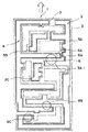
ワイヤーハーネスの相互接続を行う電気接続箱は、上部ケースと下部ケースからなるケース本体を備え、このケース本体の内部にバスバー回路板が多層積層した状態で収容され、電気接続箱(バスバー回路板)が縦置きに配置されている。各バスバー回路板は、技術文献として明確に示されたものはないが、実際に使用されているものとして図3に示す如き構成を有している。すなわち、バスバー回路板1は、絶縁材によって構成される絶縁基板2に、低い電圧を供給するバスバー3と高い電圧を供給するバスバー4とを配設して構成されている。このバスバー3、バスバー4は、図示していないがバスバー回路板1に対して垂直方向の向きに複数の分岐タブを有し、これらは絶縁基板2のタブ挿通孔を貫通して上部ケースまたは下部ケースの外面に突出し、コネクタ結合部、ヒューズ結合部、リレー結合部などの各種結合部内に配列収納され、ワイヤーハーネス端末のコネクタ、ヒューズ、リレーなどの部品と接続される。絶縁基板2は、その板面に対向するリブ5によって区画形成されたバスバー配設溝を有し、このバスバー配設溝に配設されたバスバー3、バスバー4は溶着ボスにより固定される。
【0003】
このような従来のバスバー回路板1にあっては、絶縁基板2にバスバー3、バスバー4をそれぞれ供給する電圧の電位差を考慮することなく設置している。このためバスバー回路板1にあっては、絶縁基板2上に、バスバー3とバスバー4とが整然とした状態で配設されていない。
【0004】
【発明が解決しようとする課題】
このようなバスバー回路板1にあっては、電気接続箱内部に水分の浸入があると絶縁基板2に配設されているバスバー3、バスバー4の隣接しているバスバー間6A、6B、6Cにおいてリークが発生する。このバスバー間におけるリークの発生は、バスバー3、4に銅の酸化生成物を生じさせる。この銅の酸化生成物の発生は、高い電圧を供給するバスバー4で多い。
【0005】
この銅の酸化生成物は粉状のため、図4、図5に示す如く、電気接続箱内に浸入した水分7によってバスバー間6A、6B、6Cのリブ5を乗り越えてバスバー3とバスバー4との間を流れる。また、この銅の酸化生成物は、導電性を有しているため、この銅の酸化生成物が水分と共にバスバー間6A、6B、6C、6Dのリブ5を乗り越えて流れたとき、バスバー3とバスバー4との間でショート(短絡)を起こしアーク(火花)が発生する虞がある。このようにアーク(火花)が発生すると、それに接続されている素子、装置等に影響を与えてしまう恐れがある。
【0006】
特に、図3に図示のバスバー間6Aでは、高い電位を持つバスバー4Aが低い電位を持つバスバー3A−1の位置より図示矢印で示す鉛直方向上側に配置される場合がある。この場合、高い電位を持つバスバー4Aで生じた銅の酸化生成物が浸入した水分と一緒に流れ、リブを乗り越え低い電位を持つバスバー3A−1側に流れる。したがって、バスバー間6Aでは、バスバー4とバスバー3の間で電位差があることによって、バスバー間ショート(短絡)を起こしアーク(火花)が発生する可能性がある。
【0007】
本発明の目的は、バスバーに銅の酸化生成物が発生するのを低減し、バスバー間でのアーク(火花)の発生を防止することのできる電気接続箱を提供することにある。
【0008】
【課題を解決するための手段】
上記課題を解決するため請求項1記載の電気接続箱は、絶縁基板上の全体に渡って高低2種類の異なる電位を持つ複数のバスバーを混合配置してなるバスバー回路板を備えた電気接続箱において,
前記バスバー回路板を鉛直方向縦置きに配設するとともに、高い電位を持つバスバーと低い電位を持つバスバーを水平方向に隣接して設置し,
前記絶縁基板の板面に対向して前記複数のバスバーを区画配設する複数のリブを設け,
前記リブによって、前記低い電位を持つバスバーを配設する低電位用バスバー配設溝と、前記高い電位を持つバスバーを配設する高電位用バスバー配設溝をそれぞれ区画して形成し,
前記互いに隣接して水平方向に形成される前記低い電位を持つバスバーを配設する低電位用バスバー配設溝と、前記高い電位を持つバスバーを配設する高電位用バスバー配設溝とが互いに入り込む箇所においては、前記低電位用バスバー配設溝が前記高電位用バスバー配設溝の鉛直方向上側に配置して形成し,
前記低電位用バスバー配設溝に低い電位を持つバスバーを配設し、前記高電位用バスバー配設溝に高い電位を持つバスバーを配設してなることを特徴とするものである。
このように構成することにより、請求項1に記載された本発明によれば、高い電位を持つバスバーで発生した銅の酸化生成物を低い電位を持つバスバー側に浸入した水分で流すことがないため、バスバー間でのアーク(火花)の発生を防止することができる。
【0009】
上記課題を解決するため請求項2記載の電気接続箱は、1つの絶縁基板上の全体に渡って少なくとも高低2種類の異なる電位を持つ複数のバスバーを配置してなるバスバー回路板を備えた電気接続箱において,
前記バスバー回路板を鉛直方向縦置きに配設し,
前記絶縁基板の板面に対向して前記低い電位を持つ複数の第1のバスバーを配索する第1のエリアを区画するリブと、前記高い電位を持つ複数の第2のバスバーを配索する第2のエリアを区画するリブと、を前記バスバー回路板を鉛直方向上下に区分して形成し,
前記第1のエリアに前記絶縁基板の板面に対向して第1のリブを設けると共に、第2のエリアに前記絶縁基板の板面に対向して第2のリブを設け,
前記第1のリブによって前記第1のエリアに前記低い電位を持つバスバーを配設する第1のバスバー配設溝と、前記第2のリブによって前記複数の第2のエリアに前記高い電位を持つバスバーを配設する複数の第2のバスバー配設溝とを区画して形成し,
前記複数の第1のバスバーを配索する第1のエリアと、前記第2のバスバーを配索する第2のエリアとを、前記第1のエリアが前記第2のエリアの鉛直方向上側になるように配置して形成し,
前記第1のエリアの前記低電位用バスバー配設溝に低い電位を持つ複数の第1のバスバーを配設し、前記第2のエリアの前記高電位用バスバー配設溝に高い電位を持つ複数の第2のバスバーを配設してなることを特徴とするものである。
このように構成することにより、請求項2に記載された本発明によれば、低い電位を持つバスバーの配置エリアを高い電位を持つバスバーの配置エリアと分離して高い電位を持つバスバーの配置エリアより鉛直方向上側に配置しているため、高い電位を持つバスバーで発生した銅の酸化生成物を低い電位を持つバスバー側に流すことがないため、バスバー間でのアーク(火花)の発生を防止することができる。
【0011】
【発明の実施の形態】
以下、図面を参照して本発明の実施の形態を説明する。
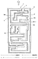
図1は本発明に係る電気接続箱の一実施の形態を示すバスバー回路板が示されている。
【0012】
図1に図示の本発明に係る電気接続箱の一実施の形態は、絶縁基板2上に少なくとも2種類の異なる電位を持つ複数のバスバー3、4を配置してなるバスバー回路板1を、電気接続箱を縦置きに配置することにより縦置き配設(図1中、上側を鉛直方向上側に配置)し、低い電位を持つバスバー3と高い電位を持つバスバー4とが水平方向に隣接して設置されているバスバー3A−1とバスバー4Aの配置を、低い電位を持つバスバー3A−1を高い電位を持つバスバー4Aの鉛直方向上側に配置するようにしたものである。
【0013】
すなわち、図1において、バスバー回路板1のバスバー3A−1とバスバー4Aの配置は、低い電位を持つバスバー3A−1を高い電位を持つバスバー4Aの鉛直方向上側に配置してある。これは、図3に図示の従来例として示したバスバー回路板1のバスバー3A−1とバスバー4Aの配置関係とは異なっている。すなわち、図3に図示の従来例として示したバスバー回路板1のバスバー3A−1とバスバー4Aの配置関係は、高い電位を持つバスバー4Aが低い電位を持つバスバー3A−1の位置より鉛直方向上側に配置してある。この従来例のバスバー3A−1とバスバー4Aの配置を設計変更して、低い電位を持つバスバー3A−1を高い電位を持つバスバー4Aの鉛直方向上側に配置したものである。
【0014】
したがって、本実施の形態によれば、浸入した水分で、高い電位を持つバスバー4Aで発生した銅の酸化生成物を低い電圧を供給するバスバー3A−1側に流すことをなくすことができる。
【0015】
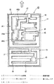
図2は本発明に係る電気接続箱の他の実施の形態を示すバスバー回路板が示されている。
【0016】
図2に図示の本発明に係る電気接続箱の他の実施の形態は、絶縁基板上に少なくとも2種類の異なる電位を持つ複数のバスバーを配置してなるバスバー回路板を縦置きに配設し、絶縁基板の複数のバスバーの配置領域を低い電位を持つ第1のエリアと高い電位を持つ第2のエリアとに区分し、第1のエリアを絶縁基板に配置する際に、第2のエリアより図示矢印で示す鉛直方向上側に配置したものである。
【0017】
図2において、バスバー回路板10は、絶縁材によって構成される絶縁基板11を有し、この絶縁基板11には、低い電位を持つ第1のエリア12と、高い電位を持つ第2のエリア13とが設けられている。この第1のエリア12と第2のエリア13は、絶縁基板11上での配置関係が、第1のエリアが第2のエリアより鉛直方向上側に配置してある。そして、この第1のエリア12には、低い電位を持つバスバー14が配設されている。このバスバー14は、図2では、バスバー14A、14B、14Cの3つのバスバーからなっている。すなわち、第1のエリア12には、複数の低い電位を持つバスバー14A、14B、14Cを設けている。
また、第2のエリア13には、高い電位を持つバスバー15が配設されている。このバスバー15は、図2では、全体がつながった1個のバスバーで構成されている。
【0018】
絶縁基板11は、第1のエリア12及び第2のエリア13に、それぞれその板面に対向するリブ16、17によって区画形成されたバスバー配設溝18、19を有し、このバスバー配設溝18、19に配設されたバスバー14、バスバー15は図示されていない溶着ボスにより固定されている。
【0019】
したがって、本実施の形態によれば、低い電位を持つバスバーの配置エリアを高い電位を持つバスバーの配置エリアと分離して高い電位を持つバスバーの配置エリアより鉛直方向上側に配置しているため、高い電位を持つバスバーで発生した銅の酸化生成物を低い電圧を供給するバスバー側に流すことがないため、バスバー14、15に銅の酸化生成物が発生するのを低減し、バスバー14、15間でのアーク(火花)の発生を防止することができる。
【0020】
【発明の効果】
以上説明したように構成されているので、以下のような効果を奏する。
【0021】
請求項1に記載の発明によれば、高い電位を持つバスバーで発生した銅の酸化生成物を低い電位を持つバスバー側に浸入した水分で流すことがないため、バスバー間でのアーク(火花)の発生を防止することができる。
【0022】
請求項2記載の発明によれば、低い電位を持つバスバーの配置エリアを高い電位を持つバスバーの配置エリアと分離して高い電位を持つバスバーの配置エリアより鉛直方向上側に配置しているため、高い電位を持つバスバーで発生した銅の酸化生成物を低い電位を持つバスバー側に流すことがないため、バスバー間でのアーク(火花)の発生を防止することができる。
【図面の簡単な説明】
【図1】本発明による電気接続箱の一実施の形態を示すバスバー回路板の正面図である。
【図2】本発明による電気接続箱の他の実施の形態を示すバスバー回路板の正面図である。
【図3】従来の電気接続箱のバスバー回路板の正面図である。
【図4】図3に図示のバスバー間を水分が流れる状態を示す正面図である。
【図5】図4に図示の断面図である。
【符号の説明】
1………………………………………バスバー回路板
2………………………………………絶縁基板
3,4…………………………………バスバー
5………………………………………リブ
10……………………………………バスバー回路板
11……………………………………絶縁基板
12……………………………………第1のエリア
13……………………………………第2のエリア
14,15……………………………バスバー[0001]
BACKGROUND OF THE INVENTION
The present invention relates to an electrical junction box that interconnects wire harnesses, and more particularly, to an electrical junction box that can reduce the occurrence of leakage between bus bars having different voltages.
[0002]
[Prior art]
An electrical junction box for interconnecting wire harnesses has a case body composed of an upper case and a lower case, and is accommodated in a multi-layered state with a bus bar circuit board inside the case body, and an electrical junction box (bus bar circuit board). Are arranged vertically. Each bus bar circuit board is not clearly shown in the technical literature, but has a configuration as shown in FIG. 3 as actually used. That is, the bus
[0003]
In such a conventional bus
[0004]
[Problems to be solved by the invention]
In such a bus
[0005]
Since this copper oxidation product is in the form of powder, as shown in FIGS. 4 and 5, the
[0006]
In particular, in the
[0007]
An object of the present invention is to provide an electrical junction box that can reduce the generation of copper oxidation products in bus bars and prevent the occurrence of arcs (sparks) between bus bars.
[0008]
[Means for Solving the Problems]
In order to solve the above problems, an electrical junction box according to
The bus bar circuit board is disposed vertically vertically , and a bus bar having a high potential and a bus bar having a low potential are installed adjacent to each other in the horizontal direction .
Provided with a plurality of ribs for partitioning the plurality of bus bars facing the plate surface of the insulating substrate,
By the ribs, and the low-potential bus bar distribution設溝disposing a bus bar having said low potential, the high potential bus bar distribution設溝disposing a bus bar having said higher potential formed by partitions, respectively,
Wherein a low-potential bus bar distribution設溝disposing a bus bar having said low potential that is formed horizontally adjacent to each other, and the high-potential bus bar distribution設溝disposing a bus bar having said high potential from each other in the portion that enters the low potential busbar distribution設溝it is formed by arranging in the vertical direction upper side of the high potential bus bar distribution設溝,
The one in which the bus bars having a low potential to a low potential busbar distribution設溝arranged, characterized Rukoto such by disposing a bus bar having a high potential to the high potential bus bar distribution設溝.
With this configuration, according to the present invention described in
[0009]
In order to solve the above-mentioned problems, an electrical junction box according to
The bus bar circuit board is arranged vertically vertically,
A rib that divides a first area in which the plurality of first bus bars having the low potential is arranged facing the plate surface of the insulating substrate, and a plurality of second bus bars having the high potential are arranged. A rib that divides a second area , and is formed by dividing the bus bar circuit board vertically up and down ,
In the first area, a first rib is provided to face the plate surface of the insulating substrate, and in the second area, a second rib is provided to face the plate surface of the insulating substrate,
A first bus bar disposition groove for disposing the bus bar having the low potential in the first area by the first rib, and the high potential in the plurality of second areas by the second rib. and a plurality of second bus bar arrangement設溝disposing a bus bar formed by Gu image,
A first area in which the plurality of first bus bars are routed and a second area in which the second bus bar is routed , and the first area is on the upper side in the vertical direction of the second area. Arranged to form
It disposed the first bus bar of multiple having a low potential to the low potential busbar distribution設溝of the first area, having a high potential to the high potential bus bar distribution設溝of the second area and it is characterized in Rukoto such by arranging the second bus bar of the multiple.
With this configuration, according to the second aspect of the present invention, the bus bar arrangement area having a high potential is separated from the bus bar arrangement area having a high potential. Since it is arranged on the upper side in the vertical direction, the oxidation product of copper generated in the bus bar with high potential does not flow to the bus bar side with low potential, thus preventing arcs (sparks) from occurring between the bus bars. can do.
[0011]
DETAILED DESCRIPTION OF THE INVENTION
Embodiments of the present invention will be described below with reference to the drawings.
FIG. 1 shows a bus bar circuit board showing an embodiment of an electrical junction box according to the present invention.
[0012]
An embodiment of the electrical junction box according to the present invention shown in FIG. 1 is an electrical connection box comprising a bus
[0013]
That is, in FIG. 1, the
[0014]
Therefore, according to the present embodiment, it is possible to prevent the copper oxidation product generated in the
[0015]
FIG. 2 shows a bus bar circuit board showing another embodiment of the electrical junction box according to the present invention.
[0016]
In another embodiment of the electric junction box according to the present invention shown in FIG. 2, a bus bar circuit board in which a plurality of bus bars having at least two different potentials are arranged on an insulating substrate is arranged vertically. When the arrangement area of the plurality of bus bars on the insulating substrate is divided into a first area having a low potential and a second area having a high potential, the second area is arranged when the first area is arranged on the insulating substrate. Further, it is arranged on the upper side in the vertical direction indicated by the arrow in the figure.
[0017]
In FIG. 2, the bus
A
[0018]
The insulating substrate 11 has bus
[0019]
Therefore, according to the present embodiment, the arrangement area of the bus bar having a low potential is separated from the arrangement area of the bus bar having a high potential and is arranged vertically above the arrangement area of the bus bar having a high potential. Since the copper oxidation product generated in the bus bar having a high potential is not passed to the bus bar side supplying the low voltage, the generation of copper oxidation product in the bus bars 14 and 15 is reduced, and the bus bars 14 and 15 are reduced. Generation of arcs (sparks) can be prevented.
[0020]
【The invention's effect】
Since it is configured as described above, the following effects can be obtained.
[0021]
According to the first aspect of the present invention, since the copper oxidation product generated in the bus bar having a high potential is not caused to flow by the moisture that has entered the bus bar side having a low potential, an arc (spark) between the bus bars is prevented. Can be prevented.
[0022]
According to the invention of
[Brief description of the drawings]
FIG. 1 is a front view of a bus bar circuit board showing an embodiment of an electrical junction box according to the present invention.
FIG. 2 is a front view of a bus bar circuit board showing another embodiment of the electrical junction box according to the present invention.
FIG. 3 is a front view of a bus bar circuit board of a conventional electrical junction box.
4 is a front view showing a state in which moisture flows between the bus bars shown in FIG. 3; FIG.
FIG. 5 is a cross-sectional view illustrated in FIG. 4;
[Explanation of symbols]
1 ……………………………………… Bus
Claims (2)
前記バスバー回路板を鉛直方向縦置きに配設するとともに、高い電位を持つバスバーと低い電位を持つバスバーを水平方向に隣接して設置し,
前記絶縁基板の板面に対向して前記複数のバスバーを区画配設する複数のリブを設け,
前記リブによって、前記低い電位を持つバスバーを配設する低電位用バスバー配設溝と、前記高い電位を持つバスバーを配設する高電位用バスバー配設溝をそれぞれ区画して形成し,
前記互いに隣接して水平方向に形成される前記低い電位を持つバスバーを配設する低電位用バスバー配設溝と、前記高い電位を持つバスバーを配設する高電位用バスバー配設溝とが互いに入り込む箇所においては、前記低電位用バスバー配設溝が前記高電位用バスバー配設溝の鉛直方向上側に配置して形成し,
前記低電位用バスバー配設溝に低い電位を持つバスバーを配設し、前記高電位用バスバー配設溝に高い電位を持つバスバーを配設してなる
ことを特徴とする電気接続箱。In the electrical connection box having a bus bar circuit board comprising a plurality of bus bars by mixing arrangement having a high and low two different potentials throughout on the insulating substrate,
The bus bar circuit board is disposed vertically vertically , and a bus bar having a high potential and a bus bar having a low potential are installed adjacent to each other in the horizontal direction .
Provided with a plurality of ribs for partitioning the plurality of bus bars facing the plate surface of the insulating substrate,
By the ribs, and the low-potential bus bar distribution設溝disposing a bus bar having said low potential, the high potential bus bar distribution設溝disposing a bus bar having said higher potential formed by partitions, respectively,
Wherein a low-potential bus bar distribution設溝disposing a bus bar having said low potential that is formed horizontally adjacent to each other, and the high-potential bus bar distribution設溝disposing a bus bar having said high potential from each other in the portion that enters the low potential busbar distribution設溝it is formed by arranging in the vertical direction upper side of the high potential bus bar distribution設溝,
Electrical connection box, characterized in that said bus bar having a lower potential to the low potential busbar distribution設溝disposed, ing by arranging bus bars having a high potential to the high potential bus bar distribution設溝.
前記バスバー回路板を鉛直方向縦置きに配設し,
前記絶縁基板の板面に対向して前記低い電位を持つ複数の第1のバスバーを配索する第1のエリアを区画するリブと、前記高い電位を持つ複数の第2のバスバーを配索する第2のエリアを区画するリブと、を前記バスバー回路板を鉛直方向上下に区分して形成し,
前記第1のエリアに前記絶縁基板の板面に対向して第1のリブを設けると共に、第2のエリアに前記絶縁基板の板面に対向して第2のリブを設け,
前記第1のリブによって前記第1のエリアに前記低い電位を持つバスバーを配設する第1のバスバー配設溝と、前記第2のリブによって前記複数の第2のエリアに前記高い電位を持つバスバーを配設する複数の第2のバスバー配設溝とを区画して形成し,
前記複数の第1のバスバーを配索する第1のエリアと、前記第2のバスバーを配索する第2のエリアとを、前記第1のエリアが前記第2のエリアの鉛直方向上側になるように配置して形成し,
前記第1のエリアの前記低電位用バスバー配設溝に低い電位を持つ複数の第1のバスバーを配設し、前記第2のエリアの前記高電位用バスバー配設溝に高い電位を持つ複数の第2のバスバーを配設してなる
ことを特徴とする電気接続箱。In an electrical junction box having a bus bar circuit board in which a plurality of bus bars having at least two types of high and low potentials are arranged over one insulating substrate,
The bus bar circuit board is arranged vertically vertically,
A rib that divides a first area in which the plurality of first bus bars having the low potential is arranged facing the plate surface of the insulating substrate, and a plurality of second bus bars having the high potential are arranged. A rib that divides a second area , and is formed by dividing the bus bar circuit board vertically up and down ,
In the first area, a first rib is provided to face the plate surface of the insulating substrate, and in the second area, a second rib is provided to face the plate surface of the insulating substrate,
A first bus bar disposition groove for disposing the bus bar having the low potential in the first area by the first rib, and the high potential in the plurality of second areas by the second rib. and a plurality of second bus bar arrangement設溝disposing a bus bar formed by Gu image,
A first area in which the plurality of first bus bars are routed and a second area in which the second bus bar is routed , and the first area is on the upper side in the vertical direction of the second area. Arranged to form
It disposed the first bus bar of multiple having a low potential to the low potential busbar distribution設溝of the first area, having a high potential to the high potential bus bar distribution設溝of the second area electrical connection box, characterized in that disposed the second bus bar of the multiple ing with.
Priority Applications (3)
| Application Number | Priority Date | Filing Date | Title |
|---|---|---|---|
| JP2002262363A JP4201248B2 (en) | 2002-09-09 | 2002-09-09 | Electrical junction box |
| US10/656,322 US6866526B2 (en) | 2002-09-09 | 2003-09-08 | Electric connection box |
| DE10341586A DE10341586A1 (en) | 2002-09-09 | 2003-09-09 | Electrical connector box for cable looms/networks, has insulating board with first conducting track arranged in vertical direction on upper side of second conducting track so both tracks are adjacent |
Applications Claiming Priority (1)
| Application Number | Priority Date | Filing Date | Title |
|---|---|---|---|
| JP2002262363A JP4201248B2 (en) | 2002-09-09 | 2002-09-09 | Electrical junction box |
Publications (2)
| Publication Number | Publication Date |
|---|---|
| JP2004104892A JP2004104892A (en) | 2004-04-02 |
| JP4201248B2 true JP4201248B2 (en) | 2008-12-24 |
Family
ID=31973160
Family Applications (1)
| Application Number | Title | Priority Date | Filing Date |
|---|---|---|---|
| JP2002262363A Expired - Fee Related JP4201248B2 (en) | 2002-09-09 | 2002-09-09 | Electrical junction box |
Country Status (3)
| Country | Link |
|---|---|
| US (1) | US6866526B2 (en) |
| JP (1) | JP4201248B2 (en) |
| DE (1) | DE10341586A1 (en) |
Family Cites Families (1)
| Publication number | Priority date | Publication date | Assignee | Title |
|---|---|---|---|---|
| US4963099A (en) * | 1988-03-25 | 1990-10-16 | Yazaki Corporation | Electrical junction box |
-
2002
- 2002-09-09 JP JP2002262363A patent/JP4201248B2/en not_active Expired - Fee Related
-
2003
- 2003-09-08 US US10/656,322 patent/US6866526B2/en not_active Expired - Lifetime
- 2003-09-09 DE DE10341586A patent/DE10341586A1/en not_active Ceased
Also Published As
| Publication number | Publication date |
|---|---|
| US6866526B2 (en) | 2005-03-15 |
| US20040127077A1 (en) | 2004-07-01 |
| DE10341586A1 (en) | 2004-04-01 |
| JP2004104892A (en) | 2004-04-02 |
Similar Documents
| Publication | Publication Date | Title |
|---|---|---|
| US9144161B2 (en) | Switchgear | |
| US7160118B2 (en) | Electric junction box | |
| JP2003009347A (en) | Electrical junction box | |
| CN106170894B (en) | Junction Box | |
| JP4201248B2 (en) | Electrical junction box | |
| JP6173579B2 (en) | Busbar structure and switchboard using the same | |
| CN101821918B (en) | Power distribution apparatus | |
| CN218498524U (en) | Busbar and related switch board thereof | |
| CN1054477C (en) | Distributor for electrical power supply of series of switchgear apparatuses | |
| US20090298309A1 (en) | Electric Connection Box | |
| JP3940316B2 (en) | Electrical junction box for mounting different voltage fuses | |
| JP2004127704A (en) | Fusible link unit | |
| JPH0317548Y2 (en) | ||
| JP3298513B2 (en) | Electrical junction box | |
| JP7545162B2 (en) | Distribution Board | |
| JP3781978B2 (en) | Switchboard for ship's generator | |
| JP3284157B2 (en) | Switchboard | |
| CN219203080U (en) | Fuse box, complete vehicle circuit and vehicle | |
| JP7382891B2 (en) | DC switchboard | |
| US20250253073A1 (en) | Panel board having insulating plate | |
| KR20120017372A (en) | Multi-fuse | |
| JP3900868B2 (en) | Junction box | |
| JP3175638B2 (en) | Busbar mounting structure | |
| KR200409804Y1 (en) | Circuit Pattern of Insulation Plate for Junction Box | |
| JP4598376B2 (en) | Trunk board |
Legal Events
| Date | Code | Title | Description |
|---|---|---|---|
| A621 | Written request for application examination |
Free format text: JAPANESE INTERMEDIATE CODE: A621 Effective date: 20050126 |
|
| A977 | Report on retrieval |
Free format text: JAPANESE INTERMEDIATE CODE: A971007 Effective date: 20070402 |
|
| A131 | Notification of reasons for refusal |
Free format text: JAPANESE INTERMEDIATE CODE: A131 Effective date: 20070620 |
|
| A521 | Written amendment |
Free format text: JAPANESE INTERMEDIATE CODE: A523 Effective date: 20070810 |
|
| A131 | Notification of reasons for refusal |
Free format text: JAPANESE INTERMEDIATE CODE: A131 Effective date: 20080402 |
|
| A521 | Written amendment |
Free format text: JAPANESE INTERMEDIATE CODE: A523 Effective date: 20080602 |
|
| A02 | Decision of refusal |
Free format text: JAPANESE INTERMEDIATE CODE: A02 Effective date: 20080702 |
|
| A521 | Written amendment |
Free format text: JAPANESE INTERMEDIATE CODE: A523 Effective date: 20080829 |
|
| A911 | Transfer of reconsideration by examiner before appeal (zenchi) |
Free format text: JAPANESE INTERMEDIATE CODE: A911 Effective date: 20080908 |
|
| TRDD | Decision of grant or rejection written | ||
| A01 | Written decision to grant a patent or to grant a registration (utility model) |
Free format text: JAPANESE INTERMEDIATE CODE: A01 Effective date: 20081001 |
|
| A01 | Written decision to grant a patent or to grant a registration (utility model) |
Free format text: JAPANESE INTERMEDIATE CODE: A01 |
|
| A61 | First payment of annual fees (during grant procedure) |
Free format text: JAPANESE INTERMEDIATE CODE: A61 Effective date: 20081003 |
|
| R150 | Certificate of patent or registration of utility model |
Ref document number: 4201248 Country of ref document: JP Free format text: JAPANESE INTERMEDIATE CODE: R150 Free format text: JAPANESE INTERMEDIATE CODE: R150 |
|
| FPAY | Renewal fee payment (event date is renewal date of database) |
Free format text: PAYMENT UNTIL: 20111017 Year of fee payment: 3 |
|
| FPAY | Renewal fee payment (event date is renewal date of database) |
Free format text: PAYMENT UNTIL: 20121017 Year of fee payment: 4 |
|
| FPAY | Renewal fee payment (event date is renewal date of database) |
Free format text: PAYMENT UNTIL: 20131017 Year of fee payment: 5 |
|
| R250 | Receipt of annual fees |
Free format text: JAPANESE INTERMEDIATE CODE: R250 |
|
| R250 | Receipt of annual fees |
Free format text: JAPANESE INTERMEDIATE CODE: R250 |
|
| R250 | Receipt of annual fees |
Free format text: JAPANESE INTERMEDIATE CODE: R250 |
|
| R250 | Receipt of annual fees |
Free format text: JAPANESE INTERMEDIATE CODE: R250 |
|
| LAPS | Cancellation because of no payment of annual fees |