JP4192169B2 - Thin keyboard keycap structure - Google Patents
Thin keyboard keycap structure Download PDFInfo
- Publication number
- JP4192169B2 JP4192169B2 JP2005211039A JP2005211039A JP4192169B2 JP 4192169 B2 JP4192169 B2 JP 4192169B2 JP 2005211039 A JP2005211039 A JP 2005211039A JP 2005211039 A JP2005211039 A JP 2005211039A JP 4192169 B2 JP4192169 B2 JP 4192169B2
- Authority
- JP
- Japan
- Prior art keywords
- end point
- base
- electrical contact
- substrate
- structure according
- Prior art date
- Legal status (The legal status is an assumption and is not a legal conclusion. Google has not performed a legal analysis and makes no representation as to the accuracy of the status listed.)
- Active
Links
Images


Classifications
-
- H—ELECTRICITY
- H01—ELECTRIC ELEMENTS
- H01H—ELECTRIC SWITCHES; RELAYS; SELECTORS; EMERGENCY PROTECTIVE DEVICES
- H01H13/00—Switches having rectilinearly-movable operating part or parts adapted for pushing or pulling in one direction only, e.g. push-button switch
- H01H13/70—Switches having rectilinearly-movable operating part or parts adapted for pushing or pulling in one direction only, e.g. push-button switch having a plurality of operating members associated with different sets of contacts, e.g. keyboard
-
- H—ELECTRICITY
- H01—ELECTRIC ELEMENTS
- H01H—ELECTRIC SWITCHES; RELAYS; SELECTORS; EMERGENCY PROTECTIVE DEVICES
- H01H13/00—Switches having rectilinearly-movable operating part or parts adapted for pushing or pulling in one direction only, e.g. push-button switch
- H01H13/50—Switches having rectilinearly-movable operating part or parts adapted for pushing or pulling in one direction only, e.g. push-button switch having a single operating member
- H01H13/52—Switches having rectilinearly-movable operating part or parts adapted for pushing or pulling in one direction only, e.g. push-button switch having a single operating member the contact returning to its original state immediately upon removal of operating force, e.g. bell-push switch
- H01H2013/525—Switches having rectilinearly-movable operating part or parts adapted for pushing or pulling in one direction only, e.g. push-button switch having a single operating member the contact returning to its original state immediately upon removal of operating force, e.g. bell-push switch using a return spring acting perpendicular to the actuating direction
-
- H—ELECTRICITY
- H01—ELECTRIC ELEMENTS
- H01H—ELECTRIC SWITCHES; RELAYS; SELECTORS; EMERGENCY PROTECTIVE DEVICES
- H01H2205/00—Movable contacts
- H01H2205/004—Movable contacts fixed to substrate
Description
本発明は情報電子製品のキーボードキーキャップ構造に関し、特に薄型キーボードキーキャップ構造に関する。 The present invention relates to a keyboard keycap structure for information electronic products, and more particularly to a thin keyboard keycap structure.
電話機、計算機、パーソナルコンピュータ、ノートブック型コンピュータ、パーソナルデジタルアシスタント(Personal Digital Assistant(PDA))、携帯電話などの情報電子製品および装置の機能を作動させるとき、一般にはキーボードキーキャップを操作して指令を入力する。そのため、キーボードのキーキャップは電子製品にとって非常に重要な操作装置の一つである。 When operating the functions of information electronic products and devices such as telephones, computers, personal computers, notebook computers, personal digital assistants (PDAs), mobile phones, etc., it is generally commanded by operating keyboard keycaps Enter. Therefore, the key cap of the keyboard is one of the operation devices that are very important for electronic products.
図1は、従来のキーボードキーキャップの圧電構造を示す断面図である。現在の電子情報製品により使用されている大部分のキーボードキーキャップはキーキャップの下方に一つの圧電構造が設置されている。その圧電構造は、塊状の弾性要素101、上部フレキシブルプリント回路基板103、中央隔離片105および下部フレキシブルプリント回路基板107を含む。上部フレキシブルプリント回路基板103および下部フレキシブルプリント回路基板107は中央隔離片105により隔離される。上部フレキシブルプリント回路基板103および下部フレキシブルプリント回路基板107上に設置される回路は、キーキャップに対応する位置に接点109a、109bを有し、中央隔離片105は、接点109aと接点109bとの間に貫通孔105aを有する。また、弾性要素101は、キーキャップの対応する位置の下方に突起部101aの塊状プラスチックを有し、キーキャップが下へ圧されると、弾性要素101の突起部101aが押されて上部フレキシブルプリント回路基板103の接点109aに当たり、中央隔離片105の貫通孔105aを介して、下部フレキシブルプリント回路基板107の接点109bと電性接続されて信号が入力される。
FIG. 1 is a cross-sectional view showing a piezoelectric structure of a conventional keyboard keycap. Most keyboard keycaps used by current electronic information products have a single piezoelectric structure below the keycap. The piezoelectric structure includes a massive
図2は、従来のキーボードキーキャップ構造を示す分解斜視図である。従来のキーボードキーキャップは、キーキャップ200と弾性要素201との間に、第1の支持板213および第2の支持板215などの鋏形またはブリッジ形の支持構造がさらに設置され、キーキャップ200に対応した圧電構造に接続される。
FIG. 2 is an exploded perspective view showing a conventional keyboard keycap structure. In the conventional keyboard keycap, a saddle-shaped or bridge-shaped support structure such as a
しかし、上述の多層構造のキーキャップ構造は、部品と材料の費用が高くて組み立てが不便である上、キーキャップが一定の厚さを備えていたために、薄型及び小型の電子情報製品を望むユーザのニーズを満たすことができなかった。 However, the above-mentioned keycap structure having a multilayer structure is expensive for parts and materials, is inconvenient to assemble, and the keycap has a certain thickness, so that a user who desires a thin and small electronic information product. Could not meet the needs of.
そのため、組み立てが容易で、必要な部品が少ない薄型キーボードキーキャップが求められていた。 Therefore, there has been a demand for a thin keyboard keycap that is easy to assemble and requires few parts.
本発明の主な目的は、組み立てが容易で必要な部品が少なく、電子情報製品に求められている薄型及び小型のニーズを満たす薄型キーボードキーキャップを提供することにある。 SUMMARY OF THE INVENTION The main object of the present invention is to provide a thin keyboard keycap that can be easily assembled and has a small number of necessary parts and meets the needs for thinness and smallness required for electronic information products.
上述の目的を達成するため、本発明の薄型キーボードキーキャップ構造は、基板、フレキシブルプリント回路層およびキーキャップを少なくとも備える。基板は、第1の部分、ベースおよび第2の部分を少なくとも含み、第1の部分は第2の部分に対応し、第1の部分および第2の部分はそれぞれベースに接続され、第1の部分および第2の部分のうちの少なくともどちらか一つはベースから突出されてベースと一角度を形成する。第1の部分は第1の端点を有し、第2の部分は第2の端点を有し、第1の端点と第2の端点とは位置が互いに合わされて所定の距離で離される。そして、第1の部分および第2の部分のうちの少なくともどちらか一つが変形されることにより、第1の端点と第2の端点とは接触される。フレキシブルプリント回路層は、第1の端点上に固定された第1の電性接点および第2の端点上に固定された第2の電性接点を含み、第1の端点と第2の端点とが接触されると、第1の電性接点と第2の電性接点とが電性接続される。キーキャップは、基板上に設置されて少なくともどちらか一つの接続部を有し、基板から突出された第1の部分および第2の部分のうちの少なくともどちらか一つに接続される。 To achieve the above object, the thin keyboard keycap structure of the present invention includes at least a substrate, a flexible printed circuit layer, and a keycap. The substrate includes at least a first portion, a base, and a second portion, the first portion corresponds to the second portion, the first portion and the second portion are each connected to the base, and the first portion At least one of the portion and the second portion protrudes from the base to form an angle with the base. The first portion has a first end point, the second portion has a second end point, and the first end point and the second end point are aligned with each other and separated by a predetermined distance. Then, by deforming at least one of the first part and the second part, the first end point and the second end point are brought into contact with each other. The flexible printed circuit layer includes a first electrical contact secured on the first endpoint and a second electrical contact secured on the second endpoint, the first endpoint and the second endpoint Is contacted, the first electrical contact and the second electrical contact are electrically connected. The key cap is disposed on the substrate and has at least one connection portion, and is connected to at least one of the first portion and the second portion protruding from the substrate.
キーキャップが圧されると接続部が力を受け、基板から突出されている第1の部分および第2の部分のうちの少なくともどちらか一つが変形されることにより、第1の電性接点と第2の電性接点とが電性接続される。 When the key cap is pressed, the connection portion receives a force, and at least one of the first portion and the second portion protruding from the substrate is deformed, whereby the first electrical contact and The second electrical contact is electrically connected.
キーキャップがリリースされると、基板の変形ポテンシャルエネルギーにより、第1の部分および第2の部分のうちの少なくともどちらか一つを元の位置まで戻し、第1の電性接点と第2の電性接点との間の電性接続を切断する。 When the key cap is released, at least one of the first portion and the second portion is returned to the original position by the deformation potential energy of the substrate, and the first electrical contact and the second electrical contact are returned. Disconnect the electrical connection with the sexual contact.
上述したことから分かるように、本発明の薄型キーボードキーキャップは、基板の変形ポテンシャルエネルギーで従来技術における弾性要素を代替し、従来技術で用いられていた弾性要素を固定するための支持構造を省略して、上下部のフレキシブルプリント回路基板を一層の回路板に整合する。そのため、必要な部品を減らすことができるだけでなく、キーボードも薄型化されるため、上述した発明の目的を達成することができる。 As can be seen from the above, the thin keyboard keycap of the present invention replaces the elastic element in the prior art with the deformation potential energy of the substrate, and omits the support structure for fixing the elastic element used in the prior art. Then, the upper and lower flexible printed circuit boards are aligned with a single circuit board. Therefore, not only the necessary parts can be reduced, but also the keyboard can be thinned, so that the object of the invention described above can be achieved.
(第1実施形態)
図3Aおよび図3Bは、本発明の第1実施形態によるキーボードキーキャップ構造を示す断面図である。
(First embodiment)
3A and 3B are cross-sectional views illustrating a keyboard keycap structure according to the first embodiment of the present invention.
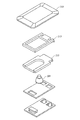
第1実施形態の薄型キーボードキーキャップ構造は、基板302、フレキシブルプリント回路層304およびキーキャップ300を少なくとも含む。
The thin keyboard keycap structure of the first embodiment includes at least a
基板302は、例えば鉄板、アルミニウム板、プラスチック板および半導体板からなる群から選ばれる一種以上を含む弾性を有する金属板または非金属板からなる。また、本実施形態の基板302はアルミニウム板からなる。
The
基板302は、第1の部分302a、第2の部分302bおよびベース302cを少なくとも含み、第1の部分302aは第2の部分302bに対応し、第1の部分302aおよび第2の部分302bはそれぞれベース302cに接続され、第1の部分302aおよび第2の部分302bのうちの少なくともどちらか一つはベース302cから突出されている。本実施形態の第1の部分302aおよび第2の部分302bは、ベース302c上から突出されてベース302cと形成する角度は90度でなく、例えば120度などである。第1の部分302aおよび第2の部分302bの厚さは、実質上0.3mmである。
The
第1の部分302aは第1の端点306aを有し、第2の部分302bは第2の端点306bを有し、第1の端点306aと第2の端点306bとは位置が互いに合わされ、第1の端点306aと第2の端点306bとは所定の距離で離されているため互いに接続されていない。そして、第1の端点306aおよび第2の端点306bのうちの少なくともどちらか一つが変形されることにより、第1の端点306aと第2の端点306bとが接触される。
The
フレキシブルプリント回路層304は、基板302上に設置され、第1の端点306a上に固定された第1の電性接点308aおよび第2の端点306b上に固定された第2の電性接点308bを含み、第1の端点306aと第2の端点306bとが接触されると、第1の電性接点308aと第2の電性接点308bとが電性接続される。本実施形態のフレキシブルプリント回路層304は、基板302上に塗布された薄膜回路層である。本発明のその他の実施形態では、フレキシブルプリント回路層304は基板302上に設置されたフレキシブルプリント回路基板であり、第1の電性接点308aおよび第2の電性接点308bは、二つの金属突起部により構成されてもよい。
The flexible printed
キーキャップ300は、基板302およびフレキシブルプリント回路層304上に設置された310aおよび310bなどの接続部を少なくとも一つ有し、固定要素312により基板302上から突出されている第1の部分302aおよび第2の部分302b上へ対称に固定される。また、本実施形態の接続部310aおよび接続部310bは長さが等しい。
The
図3Bに示すように、キーキャップ300の接続部310a、310bが力を受けると、基板から突出されている第1の部分302aおよび第2の部分302bが圧されて変形され、第1の電性接点308aと第2の電性接点308bとが電性接続される。
As shown in FIG. 3B, when the connecting
キーキャップ300がリリースされると、基板302の変形ポテンシャルエネルギーにより、第1の部分302aおよび第2の部分302bが元の位置に戻されて、第1の電性接点308aと第2の電性接点308bとの間の電性接続が切断される(図3Aに示す)。
When the
(第2実施形態)
図4Aおよび図4Bは、本発明の第2実施形態によるキーボードキーキャップ構造を示す断面図である。
(Second Embodiment)
4A and 4B are cross-sectional views illustrating a keyboard keycap structure according to a second embodiment of the present invention.
図4Aおよび図4Bに示すように、第2実施形態の構造は、第1実施形態と類似しており、基板の第1の部分および第2の部分の配置方式のみが異なる。 As shown in FIGS. 4A and 4B, the structure of the second embodiment is similar to that of the first embodiment, and only the arrangement method of the first and second portions of the substrate is different.
第2実施形態の薄型キーボードキーキャップ構造は、基板402、フレキシブルプリント回路層404およびキーキャップ400を少なくとも含む。
The thin keyboard keycap structure of the second embodiment includes at least a
基板402は、例えば鉄板、アルミニウム板、プラスチック板および半導体板からなる群から選ばれる一種以上を含む弾性を有する金属板または非金属板からなる。本実施形態の基板402はアルミニウム板からなる。
The
基板402は、第1の部分402a、第2の部分402bおよびベース402cを少なくとも含み、第1の部分402aは第2の部分402bに対応し、第1の部分402aおよび第2の部分402bはそれぞれベース402cへ接続され、第1の部分402aおよび第2の部分402bのうちの少なくともどちらか一つはベース402cから突出されている。本実施形態の第1の部分402aおよび第2の部分402bは、ベース402c上に突出され、第1の部分402aとベース402cとにより形成される第1の角度は120度などであり、第2の部分402bとベース402cとにより形成される第2の角度は110度などである。第1の部分402aおよび第2の部分402bの厚さは、実質上0.3mmである。
The
第1の部分402aは第1の端点406aを有し、第2の部分402bは第2の端点406bを有し、第1の端点406aと第2の端点406bとは位置が互いに合わされ、第1の端点406aと第2の端点406bとは所定の距離で離されているため互いに接続されていない。そして、第1の部分402aおよび第2の部分402bのうちの少なくともどちらか一つが変形されることにより、第1の端点406aと第2の端点406bとが接触される。
The
フレキシブルプリント回路層404は、第1の端点406a上に固定された第1の電性接点408aおよび第2の端点406b上に固定された第2の電性接点408bを含み、第1の端点406aと第2の端点406bとが接触されると、第1の電性接点408aと第2の電性接点408bとが電性接続される。本実施形態のフレキシブルプリント回路層404は、基板402上に塗布された薄膜回路層である。本発明のその他の実施形態では、フレキシブルプリント回路層404は基板402上に設置されたフレキシブルプリント回路基板であり、第1の電性接点408aおよび第2の電性接点408bは、二つの金属突起部により構成されてもよい。
The flexible printed
キーキャップ400は、基板402上に設置された410aおよび410bなどの接続部を少なくとも一つ有し、固定要素412により基板402上に突出されている第1の部分402aおよび第2の部分402b上へ対称に固定される。また、本実施形態の接続部410aと接続部410bとは対称でない。
The
図4Bに示すように、キーキャップ400の接続部410a、410bが力を受けると、基板から突出されている第1の部分402aおよび第2の部分402bが圧されて変形されることにより、第1の電性接点408aと第2の電性接点408bとは電性接続される。
As shown in FIG. 4B, when the connecting
キーキャップ400がリリースされると、基板402の変形ポテンシャルエネルギーにより、第1の部分402aおよび第2の部分402bが元の位置に戻され、第1の電性接点408aと第2の電性接点408bとの間の電性接続が切断される(図4Aに示す)。
When the
(第3実施形態)
図5Aおよび図5Bは、本発明の第3実施形態によるキーボードキーキャップ構造を示す断面図である。
(Third embodiment)
5A and 5B are cross-sectional views illustrating a keyboard keycap structure according to a third embodiment of the present invention.
図5Aおよび図5Bに示すように、第3実施形態の構造は、第1実施形態と類似しており、基板の第1の部分および第2の部分の配置方式のみが異なる。 As shown in FIGS. 5A and 5B, the structure of the third embodiment is similar to that of the first embodiment, and only the arrangement of the first part and the second part of the substrate is different.
第3実施形態の薄型キーボードキーキャップ構造は、基板502、フレキシブルプリント回路層504およびキーキャップ500を少なくとも含む。
The thin keyboard keycap structure of the third embodiment includes at least a
基板502は、例えば鉄板、アルミニウム板、プラスチック板および半導体板からなる群から選ばれる一種以上を含む弾性を有する金属板または非金属板からなる。また、本実施形態の基板502はアルミニウム板からなる。
The
基板502は、第1の部分502a、第2の部分502bおよびベース502cを少なくとも含み、第1の部分502aは第2の部分502bに対応し、第1の部分502aおよび第2の部分502bはそれぞれベース502cに接続され、第1の部分502aおよび第2の部分502bのうちの少なくともどちらか一つはベース502cから突出されている。本実施形態では第1の部分502aのみが基板502上から突出され、第1の部分502aとベース502cとにより形成される第1の角度は120度などであり、第2の部分502bとベース502cとは同一平面を形成する。第1の部分502aの厚さは、実質上0.3mmである。
The
第1の部分502aは第1の端点506aを有し、第2の部分502bは第2の端点506bを有し、第1の端点506aと第2の端点506bとは位置が互いに合わされ、第1の端点506aと第2の端点506bとは所定の距離で離されているため互いに接続されていない。そして、第1の部分502aおよび第2の部分502bのうちの少なくともどちらか一つが変形されることにより、第1の端点506aと第2の端点506bとが接触される。
The
フレキシブルプリント回路層504は、第1の端点506a上に固定された第1の電性接点508aおよび第2の端点506b上に固定された第2の電性接点508bを含み、第1の端点506aと第2の端点506bとが接触されると、第1の電性接点508aと第2の電性接点508bとが電性接続される。本実施形態のフレキシブルプリント回路層504は、基板502上に塗布された薄膜回路層である。本発明のその他の実施形態では、フレキシブルプリント回路層504は基板502上に設置されたフレキシブルプリント回路基板であり、第1の電性接点508aおよび第2の電性接点508bは、二つの金属突起部により構成されてもよい。
The flexible printed
キーキャップ500は、基板502上に設置された510などの接続部を少なくとも一つ有し、固定要素512により基板502上から突出されている第1の部分502a上へ固定される。
The
図5Bに示すように、キーキャップ500の接続部510が力を受けると、基板502から突出されている第1の部分502aが圧されて変形されることにより、第1の電性接点508aと第2の電性接点508bとが電性接続される。
As shown in FIG. 5B, when the connecting
キーキャップ500がリリースされると、基板502の変形ポテンシャルエネルギーにより、第1の部分502aが元の位置に戻され、第1の電性接点508aと第2の電性接点508bとの間の電性接続が切断される(図5Aに示す)。
When the
上述したことから分かるように、本発明の好適な実施形態は基板を使用し、基板の表面から突出された一部の変形ポテンシャルエネルギーにより、キーキャップが再び押されると元の位置に戻ることを利用して、従来技術の弾性要素を代替するとともに、従来技術の上部および下部のフレキシブルプリント回路基板を一層の回路板に整合し、従来技術で用いられていた弾性要素の支持構造を省略して、キーボードを薄型化することができる。 As can be seen from the above, the preferred embodiment of the present invention uses a substrate, and some deformation potential energy protruding from the surface of the substrate returns to its original position when the keycap is pressed again. Use it to replace the elastic elements of the prior art, align the upper and lower flexible printed circuit boards of the prior art with a single circuit board, and omit the support structure of the elastic elements used in the prior art The keyboard can be thinned.
よって、本発明の好適な実施形態は、部品費用を節約して薄型のキーボードキーキャップ構造を提供することができる。 Thus, the preferred embodiment of the present invention can provide a thin keyboard keycap structure with reduced component costs.
本発明では好適な実施形態を前述の通り開示したが、これらは決して本発明を限定するものではなく、当該技術を熟知するものなら誰でも、本発明の主旨と領域を脱しない範囲内で各種の変更や修正を加えることができる。従って本発明の保護の範囲は、特許請求の範囲で指定した内容を基準とする。 In the present invention, preferred embodiments have been disclosed as described above, but these are not intended to limit the present invention in any way, and anyone who is familiar with the technology can make various modifications within the scope and spirit of the present invention. Changes and corrections can be made. Therefore, the scope of protection of the present invention is based on the contents specified in the claims.
302、402、502 基板
304、404、504 フレキシブルプリント回路層
302a、402a、502a 第1の部分
302b、402b、502b 第2の部分
302c、402c、502c ベース
306a、406a、506a、306b、406b、506b 端点
308a、408a、508a、308b、408b、508b 電性接点
310a、410a、510、310b、410b 接続部
312、412、512 固定要素
302, 402, 502
Claims (12)
前記基板を覆う所定回路を有し、前記所定回路は前記第1の端点上に固定される第1の電性接点と、前記第2の端点に固定される第2の電性接点とを少なくとも含み、前記第1の端点と前記第2の端点とが接触されると、前記第1の電性接点と前記第2の電性接点とが電性接続されるフレキシブルプリント回路層と、
前記基板上に設置され、第1の接続部を有し、前記第1の接続部の一方の端部に接続され、前記第1の接続部の他方の端部が前記ベースから突出された前記第1の部分に接続されるキーキャップと、を少なくとも備える薄型キーボードキーキャップ構造であって、
前記キーキャップが押されて前記第1の接続部が力を受けると、前記第1の接続部は前記ベースから突出されている前記第1の部分を圧して変形させ、前記第1の部分が前記第2の部分に接近するように撓んで変形されることにより、前記第1の端点と前記第2の端点とが接触され、前記第1の電性接点と前記第2の電性接点とが電性接続され、
前記キーキャップがリリースされると、前記基板が変形して貯めていたポテンシャルエネルギーが放出されることにより、前記第1の部分を元の位置に戻し、前記第1の電性接点と前記第2の電性接点との間の電性接続を切断することを特徴とする薄型キーボードキーキャップ構造。 A base, a first part and a second part, wherein the first part and the second part are connected to the base, respectively, and the first part protrudes from the base and Forming a first angle with the base, the first portion having a first endpoint, the second portion having a second endpoint, the first endpoint and the second endpoint; Are aligned with each other and separated from each other by a predetermined distance, and the first portion deforms to contact the first end point and the second end point; and
A predetermined circuit covering the substrate, wherein the predetermined circuit includes at least a first electrical contact fixed on the first end point and a second electrical contact fixed on the second end point; A flexible printed circuit layer electrically connected to the first electrical contact and the second electrical contact when the first end point and the second end point are contacted;
The first connection portion is installed on the substrate , has a first connection portion, is connected to one end portion of the first connection portion, and the other end portion of the first connection portion protrudes from the base. a keycap coupled to the first portion, and at least comprises thin keyboard keycap structure,
When the first connection portion is pushed the key cap Ru receives the force, the first connecting portion deforms by applying the first portion that protrudes from said base, said first portion Is bent and deformed so as to approach the second portion, the first end point and the second end point are brought into contact with each other, and the first electrical contact and the second electrical contact are brought into contact with each other. And are electrically connected,
When the keycap is released, the potential energy stored by the deformation of the substrate is released, thereby returning the first portion to the original position, and the first electrical contact and the second A thin keyboard keycap structure characterized by disconnecting the electrical connection between the electrical contacts of the keyboard.
Said first connecting portion is thin keyboard keycap structure according to claim 1, wherein the fixing element, characterized in that it is connected to the first portion of the substrate.
Applications Claiming Priority (1)
| Application Number | Priority Date | Filing Date | Title |
|---|---|---|---|
| TW094113727A TWI260662B (en) | 2005-04-28 | 2005-04-28 | Thin press-button structure of kyeboard |
Publications (2)
| Publication Number | Publication Date |
|---|---|
| JP2006309686A JP2006309686A (en) | 2006-11-09 |
| JP4192169B2 true JP4192169B2 (en) | 2008-12-03 |
Family
ID=37233369
Family Applications (1)
| Application Number | Title | Priority Date | Filing Date |
|---|---|---|---|
| JP2005211039A Active JP4192169B2 (en) | 2005-04-28 | 2005-07-21 | Thin keyboard keycap structure |
Country Status (3)
| Country | Link |
|---|---|
| US (1) | US7164089B2 (en) |
| JP (1) | JP4192169B2 (en) |
| TW (1) | TWI260662B (en) |
Cited By (1)
| Publication number | Priority date | Publication date | Assignee | Title |
|---|---|---|---|---|
| US7697378B2 (en) | 2005-08-30 | 2010-04-13 | Panasonic Corporation | Information reproducing device |
Families Citing this family (2)
| Publication number | Priority date | Publication date | Assignee | Title |
|---|---|---|---|---|
| TW200945391A (en) * | 2008-04-25 | 2009-11-01 | Chi Mei Comm Systems Inc | Keypad module and portable electronic device using the same |
| US8592699B2 (en) | 2010-08-20 | 2013-11-26 | Apple Inc. | Single support lever keyboard mechanism |
Family Cites Families (4)
| Publication number | Priority date | Publication date | Assignee | Title |
|---|---|---|---|---|
| US5767464A (en) * | 1996-12-05 | 1998-06-16 | Texas Instruments Incorporated | Electronic device low profile keyboard switch assembly with deployed and stored actuating mechanism |
| US5879088A (en) * | 1997-11-24 | 1999-03-09 | Key Tronic Corporation | Computer keyboard with adjustable force keystroke feature using air pressure |
| JP4295468B2 (en) * | 2001-12-21 | 2009-07-15 | ポリマテック株式会社 | Cover member for illuminated pushbutton switch |
| US7060923B2 (en) * | 2004-06-10 | 2006-06-13 | Nokia Corporation | Key |
-
2005
- 2005-04-28 TW TW094113727A patent/TWI260662B/en active
- 2005-07-21 JP JP2005211039A patent/JP4192169B2/en active Active
-
2006
- 2006-04-05 US US11/398,184 patent/US7164089B2/en active Active
Cited By (1)
| Publication number | Priority date | Publication date | Assignee | Title |
|---|---|---|---|---|
| US7697378B2 (en) | 2005-08-30 | 2010-04-13 | Panasonic Corporation | Information reproducing device |
Also Published As
| Publication number | Publication date |
|---|---|
| US20060243567A1 (en) | 2006-11-02 |
| JP2006309686A (en) | 2006-11-09 |
| US7164089B2 (en) | 2007-01-16 |
| TWI260662B (en) | 2006-08-21 |
| TW200638451A (en) | 2006-11-01 |
Similar Documents
| Publication | Publication Date | Title |
|---|---|---|
| US7541554B2 (en) | Key structure | |
| JP4359812B2 (en) | Switch-integrated casing and electronic device having the same | |
| US8410381B2 (en) | Push-on switch | |
| JP2013093313A (en) | Switch | |
| JP6051705B2 (en) | switch | |
| WO2002005302A1 (en) | El sheet and switch comprising the same | |
| US20140001021A1 (en) | Press key | |
| US7919719B2 (en) | Dome contact used in pushbutton switch | |
| JP4192169B2 (en) | Thin keyboard keycap structure | |
| JP2002107245A (en) | Force detector | |
| JP2011100549A (en) | Push switch | |
| JP4342564B2 (en) | Seat switch and its operation sheet | |
| CN100437865C (en) | Thinning keyboard press button structure | |
| JP2007179923A (en) | Metal dome holding sheet, and metal dome switch | |
| US20050211537A1 (en) | Movable contact body and panel switch using the same | |
| JPWO2004055848A1 (en) | Seat switch and its operation sheet | |
| JP2008311009A (en) | Press operation device | |
| JPS6344252B2 (en) | ||
| CN109690713B (en) | Resin structure, electronic device, and method for manufacturing resin structure | |
| US6768075B2 (en) | Membrane switch and dial operation member equipped therewith | |
| JP4221338B2 (en) | Key switch structure | |
| JP4784630B2 (en) | Switch-integrated casing and electronic device having the same | |
| JP2007220528A (en) | Movable contact structure, and push-button switch | |
| JP2006019056A (en) | Push-button device | |
| KR100925067B1 (en) | A double contact switch |
Legal Events
| Date | Code | Title | Description |
|---|---|---|---|
| A977 | Report on retrieval |
Free format text: JAPANESE INTERMEDIATE CODE: A971007 Effective date: 20080303 |
|
| A131 | Notification of reasons for refusal |
Free format text: JAPANESE INTERMEDIATE CODE: A131 Effective date: 20080311 |
|
| A521 | Request for written amendment filed |
Free format text: JAPANESE INTERMEDIATE CODE: A523 Effective date: 20080529 |
|
| TRDD | Decision of grant or rejection written | ||
| A01 | Written decision to grant a patent or to grant a registration (utility model) |
Free format text: JAPANESE INTERMEDIATE CODE: A01 Effective date: 20080826 |
|
| A01 | Written decision to grant a patent or to grant a registration (utility model) |
Free format text: JAPANESE INTERMEDIATE CODE: A01 |
|
| A61 | First payment of annual fees (during grant procedure) |
Free format text: JAPANESE INTERMEDIATE CODE: A61 Effective date: 20080919 |
|
| FPAY | Renewal fee payment (event date is renewal date of database) |
Free format text: PAYMENT UNTIL: 20110926 Year of fee payment: 3 |
|
| R150 | Certificate of patent or registration of utility model |
Free format text: JAPANESE INTERMEDIATE CODE: R150 Ref document number: 4192169 Country of ref document: JP Free format text: JAPANESE INTERMEDIATE CODE: R150 |
|
| FPAY | Renewal fee payment (event date is renewal date of database) |
Free format text: PAYMENT UNTIL: 20110926 Year of fee payment: 3 |
|
| FPAY | Renewal fee payment (event date is renewal date of database) |
Free format text: PAYMENT UNTIL: 20140926 Year of fee payment: 6 |
|
| R250 | Receipt of annual fees |
Free format text: JAPANESE INTERMEDIATE CODE: R250 |
|
| R250 | Receipt of annual fees |
Free format text: JAPANESE INTERMEDIATE CODE: R250 |
|
| R250 | Receipt of annual fees |
Free format text: JAPANESE INTERMEDIATE CODE: R250 |
|
| R250 | Receipt of annual fees |
Free format text: JAPANESE INTERMEDIATE CODE: R250 |
|
| R250 | Receipt of annual fees |
Free format text: JAPANESE INTERMEDIATE CODE: R250 |
|
| R250 | Receipt of annual fees |
Free format text: JAPANESE INTERMEDIATE CODE: R250 |