JP4190086B2 - Electronic imaging device - Google Patents
Electronic imaging device Download PDFInfo
- Publication number
- JP4190086B2 JP4190086B2 JP12884099A JP12884099A JP4190086B2 JP 4190086 B2 JP4190086 B2 JP 4190086B2 JP 12884099 A JP12884099 A JP 12884099A JP 12884099 A JP12884099 A JP 12884099A JP 4190086 B2 JP4190086 B2 JP 4190086B2
- Authority
- JP
- Japan
- Prior art keywords
- optical system
- focus detection
- mirror
- ccd
- image
- Prior art date
- Legal status (The legal status is an assumption and is not a legal conclusion. Google has not performed a legal analysis and makes no representation as to the accuracy of the status listed.)
- Expired - Fee Related
Links
Images


Classifications
-
- G—PHYSICS
- G02—OPTICS
- G02B—OPTICAL ELEMENTS, SYSTEMS OR APPARATUS
- G02B7/00—Mountings, adjusting means, or light-tight connections, for optical elements
- G02B7/28—Systems for automatic generation of focusing signals
-
- H—ELECTRICITY
- H04—ELECTRIC COMMUNICATION TECHNIQUE
- H04N—PICTORIAL COMMUNICATION, e.g. TELEVISION
- H04N23/00—Cameras or camera modules comprising electronic image sensors; Control thereof
- H04N23/50—Constructional details
- H04N23/55—Optical parts specially adapted for electronic image sensors; Mounting thereof
-
- H—ELECTRICITY
- H04—ELECTRIC COMMUNICATION TECHNIQUE
- H04N—PICTORIAL COMMUNICATION, e.g. TELEVISION
- H04N23/00—Cameras or camera modules comprising electronic image sensors; Control thereof
- H04N23/60—Control of cameras or camera modules
- H04N23/67—Focus control based on electronic image sensor signals
- H04N23/675—Focus control based on electronic image sensor signals comprising setting of focusing regions
-
- H—ELECTRICITY
- H04—ELECTRIC COMMUNICATION TECHNIQUE
- H04N—PICTORIAL COMMUNICATION, e.g. TELEVISION
- H04N25/00—Circuitry of solid-state image sensors [SSIS]; Control thereof
- H04N25/10—Circuitry of solid-state image sensors [SSIS]; Control thereof for transforming different wavelengths into image signals
- H04N25/11—Arrangement of colour filter arrays [CFA]; Filter mosaics
- H04N25/13—Arrangement of colour filter arrays [CFA]; Filter mosaics characterised by the spectral characteristics of the filter elements
- H04N25/134—Arrangement of colour filter arrays [CFA]; Filter mosaics characterised by the spectral characteristics of the filter elements based on three different wavelength filter elements
Landscapes
- Engineering & Computer Science (AREA)
- Multimedia (AREA)
- Signal Processing (AREA)
- Physics & Mathematics (AREA)
- General Physics & Mathematics (AREA)
- Optics & Photonics (AREA)
- Focusing (AREA)
- Studio Devices (AREA)
- Automatic Focus Adjustment (AREA)
Description
【0001】
【発明の属する技術分野】
この発明は、電子的撮像装置、詳しくは撮影光学系により結像される光学的な被写体像を光電変換することにより電気的な画像信号を生成する撮像素子を有してなる電子的撮像装置に適用される焦点検出装置に関するものである。
【0002】
【従来の技術】
近年、撮影光学系を透過した被写体光束によって結像される光学的な被写体像をCCD(Charge Coupled Device;電荷結合素子)等の撮像素子等を利用して電気的な信号に光電変換し、これによって生成された画像信号を所定の形態の画像データとして記録媒体等に記録し得るデジタルスチルカメラやデジタルビデオカメラ等の電子的撮像装置についての提案が種々なされており、また広く普及している。
【0003】
例えば特開平8−262564号公報には、単一の撮影光学系を透過した光束を用いて撮影記録をなすべき被写体像と、観察用の被写体像とを、それぞれ異なる位置に結像させ得るように構成した一眼レフレックスタイプの電子的撮像装置が開示されている。この電子的撮像装置は、撮像用の被写体像の結像面に撮像用の固体撮像素子等の撮像手段を設けると共に、この結像面と等価となる位置に撮像用の撮像手段とは別に、焦点検出用の撮像手段を設けるように構成している。そして、この焦点検出用の撮像手段に対して撮影光学系を透過した光束の一部を導くことで、被写体像の焦点状態を検出するTTL位相差検出方式の焦点検出手段(AF手段)を構成し、これに基づいて合焦動作を行うようにしたものである。
【0004】
また、特開平9−274130号公報によって開示されている電子的撮像装置は、主に動画像を撮影記録するいわゆるビデオムービーカメラであって、撮像用の撮像素子等の撮像手段をカメラ本体内に配置する一方、この撮像用の撮像素子等の撮像手段とは異なる別の撮像手段等によって構成されるTTL位相差検出方式の焦点検出ユニットを撮影レンズを保持するためのレンズ鏡筒の内部に配置するようにしたものである。
【0005】
【発明が解決しようとする課題】
ところが、上記特開平8−262564号公報や上記特開平9−274130号公報等によって開示される従来の電子的撮像装置では、被写体像を撮影記録するための撮像素子等の撮像手段とは別に、焦点検出を行なうための専用の撮像素子等の撮像手段を備えて構成している。
【0006】
このような構成とした場合には、電子的撮像装置全体の部品点数が多くなってしまうと共に、装置自体が大型化してしまうという問題点がある。これと同時に、撮像素子等の高価な部品を複数必要とすることから、製造コストを引き上げてしまうという問題点もある。
【0007】
本発明は、上述した点に鑑みてなされたものであって、その目的とするところは、撮影光学系により結像された被写体像を撮像素子を利用して画像信号に光電変換し、この画像信号を画像データとして記録媒体に記録する電子的撮像装置において、焦点検出を行なうための専用の撮像素子が不要となるような構成を採ることで、装置自体の小型化及び製造コストの低減化に寄与することのできる電子的撮像装置を提供することである。
【0008】
【課題を解決するための手段】
上記目的を達成するために、本発明の一態様による電子的撮像装置は、撮影レンズと、上記撮影レンズの形成する像を観察する観察光学系と、上記撮影レンズが形成した像から画像データを生成するための撮像素子と、上記撮影レンズの射出瞳を通過した光束から2つの像を上記撮像素子へ形成する焦点検出光学系と、撮影準備位置に設定されると上記観察光学系と上記焦点検出光学系へ撮影レンズの光束を導き、撮影位置に設定されると上記撮像素子へ光束を導くミラーと、上記ミラーの撮影準備位置において、上記撮像素子の出力信号より上記2つの像の間隔を検出し、上記撮影レンズの焦点調整の為のデフォーカス量を算出する焦点調整回路と、を有し、上記ミラーは更にサブミラーを有し、該サブミラーによって上記ミラーの半透過部を通過した上記撮影レンズからの光束を上記焦点検出光学系へ導くことを特徴とする。
【0011】
【発明の実施の形態】
以下、図示の実施の形態によって本発明を説明する。
図1は、本発明の第1の実施形態の電子的撮像装置における主要構成部材の配置を概略的に示す図であって、合わせて撮影光学系を透過した光束の本電子的撮像装置の内部における光路を示している。なお、図1では、図面の繁雑化を避けるために、本発明に直接関連しない構成部材については、その図示を省略し、本発明に直接関係する構成部材のみを示している。
【0012】
図1に示すように、本電子的撮像装置の前面側には、被写体からの光束(以下、被写体光束という)を集光し、同被写体光束を本電子的撮像装置の内部に導くための複数のレンズ等によって構成される撮影光学系11が配置されている。
【0013】
この撮影光学系11は、被写体像を所定の位置に結像させるために、光軸Oに沿う方向に移動することで焦点状態の調節を行なう焦点調節光学系である合焦レンズ11aと、撮影光学系11を透過する被写体光束の光量を調節する絞り部材11b等を有して構成されている。この絞り部材11bは、所定の絞り開口を保持する機能を有すると共に、完全な閉状態となることで入射する被写体光束を遮光する機能を有している。
【0014】
撮影光学系11の後方には、被写体光束に含まれる光成分のうち主に赤外光成分を除去するための赤外光カットフイルター12と、被写体光束に含まれる光成分のうちモアレ等のノイズ成分を低減させるための光学的ローパスフイルター(LPF)13が配置されている。
【0015】
さらにその後方には、一部の領域が半透過鏡部(以下、ハーフミラー部)によって形成される反射鏡からなり、撮影光学系11を透過した被写体光束を観察用の光束と焦点検出用の光束に分割し得ると共に、同被写体光束の光路外に退避することで被写体光束を通過させ得る光学部材であり分割光学系である主鏡(メインミラー)14が、その一端部を本電子的撮像装置の内部固定部材(図示せず)に対して図1の矢印X1方向に回動自在となるように配置されている。
【0016】
また、このメインミラー14の背面側の所定の位置には、上述のメインミラー14のハーフミラー部を透過した被写体光束を焦点検出光学系30へと導き得るように全反射鏡等の光学部材によって形成された副鏡(サブミラー)19が、メインミラー14に対して回動自在に設けられている。
【0017】
そして、メインミラー14の後方であって、撮影光学系11を透過した被写体光束により形成される被写体像が結像される結像面となる位置には、CCD等の固体撮像素子21(以下、単にCCD21という)を含む撮影手段が配置されている。このCCD21は、光学的な被写体像を受光して光電変換することにより電気的な画像信号を生成するものであって、例えば上述のCCD等の固体撮像素子や、MOS型センサ等、各種の固体撮像素子等を適用し得る。
【0018】
また、メインミラー14の上部側の所定の位置には、撮影光学系11からの被写体光束を受けて主に被写体像の観察を行なうためファインダー光学系が配置されている一方、下部側の所定の位置には、撮影光学系11からの被写体光束の一部を受けて、これをCCD21の受光面上の所定の位置へと導き、再結像させる焦点検出光学系30が配置されている。
【0019】
メインミラー14は、上述したように一部の領域のみがハーフミラーにより形成され、他の領域は全反射ミラー部で形成されている。この場合における一部の領域とは、サブミラー19に対応する領域であり、このハーフミラーによって形成された領域、即ちハーフミラー部では、撮影光学系11からの被写体光束が透過し得るようになっていると共に、ハーフミラー部以外の領域では、撮影光学系11からの被写体光束を全反射するようになっている。
【0020】
メインミラー14は、図1において実線で示す位置(以下、この位置を撮影準備位置という)と、同図における点線で示す位置(以下、撮影位置という)との間を固定部材(図示せず)を支点に回動するようになっている。これと同時にサブミラー19は、メインミラー14の回動に従動して、メインミラー14の位置に応じた所定の位置に配置されるようになっている。
【0021】
この場合において、メインミラー14が撮影準備位置(図1の実線位置)にあるときには、同メインミラー14は、光軸Oに対して角度略45度だけ傾けて配置されるようにしている。このときメインミラー14の反射面は、撮影光学系11の側(即ち本電子的撮像装置の前面側の被写体側)及びファインダー光学系の側に向くようになっている。
【0022】
また、このときサブミラー19は、被写体光束の光路上において、メインミラー14に対して所定の角度を有するように配置されることになる。そして、サブミラー19の反射面は、撮影光学系11の側(被写体側)及び焦点検出光学系30の側に向くようになっている。
【0023】
したがって、撮影光学系11からの被写体光束は、一部がメインミラー14の全反射面によってファインダー光学系の側に導かれると同時に、メインミラー14のハーフミラー部を透過した一部の被写体光束がサブミラー19の全反射面によって焦点検出光学系30の側に導かれるようになっている。
【0024】
これにより、メインミラー14が撮影準備位置にあるときには、メインミラー14のハーフミラー部を透過し、サブミラー19及び焦点検出光学系30を介した被写体光束のみがCCD21へと導かれるようになっている。
【0025】
一方、メインミラー14が撮影位置(図1の点線位置)にあるときには、メインミラー14及びサブミラー19は、上述したように撮影光学系11を透過した被写体光束の光路を遮らない位置へと退避するようになっている。したがって、このときの被写体光束は、全てがCCD21の側へと導かれ、同CCD21の受光面の全域に向けて照射されるようになっている。
【0026】
ファインダー光学系は、観察用の被写体像が結像する結像面近傍に配置され、被写体光束を被写体像の観察位置へと導くピント板15及びコンデンサーレンズ16と、被写体像を観察位置に導くと共に、左右像を反転させるペンタプリズム17と、ピント板15上に結像されている被写体像を拡大して、観察するのに最適な位置に結像させる接眼レンズ18等によって構成されている。
【0027】
焦点検出光学系30は、視野マスク31・フィールドレンズ32・全反射ミラー33・瞳マスク34・再結像レンズ35等によって構成されており、撮影光学系11からの被写体光束の一部であって、本電子的撮像装置が撮影準備状態に有るときに、メインミラー14及びサブミラー19の作用により導かれる焦点検出用の被写体光束から所定の形態の像をCCD21の受光面上の所定の位置に再結像させる役目をしているものである。
【0028】
ここで、本電子的撮像装置における焦点検出光学系30について、以下に詳述する。
図2・図3は、本電子的撮像装置における焦点検出光学系の構成の概念を示す側断面図及び斜視図であって、合わせて撮影光学系11を透過した被写体光束が焦点検出光学系30を介してCCD21へと到達する際の様子を概念的に示している。なお、図2・図3では、図面の繁雑化を避けるために、本焦点検出光学系30の構成及び作用を説明するのに不要と思われる構成部材、例えばメインミラー14・サブミラー19・全反射ミラー33等や焦点検出光学系30の各構成部材等を保持し、ユニット化する筐体部材等については、その図示を省略し、主要となる構成部材のみを取り出して示している。また、図2では、被写体光束の光路について、一方の射出瞳Ha側のみを図示しているが、他方(Hb側)については対称であるので、その図示を省略している。
【0029】
本電子的撮像装置における焦点検出光学系30は、焦点検出動作に寄与する焦点検出用の光束をCCD21へと導くための光学系であって、いわゆるTTL位相差検出方式の焦点検出手段の一部を構成するものである。
【0030】
図2・図3に示すように、焦点検出光学系30は、撮影光学系11(図3では図示せず)を透過した被写体光束の照射範囲を規制する視野マスク31と、この視野マスク31を通過した被写体光束を集光するフィールドレンズ32と、このフィールドレンズ32を透過した被写体光束の光路を折り曲げてCCD21の側へと導く全反射ミラー33(図2・図3では図示せず)と、被写体光束の光軸Oに対して略対称に配置され、全反射ミラー33により反射された被写体光束を二つの光束に分割する二つの開口部34a・34bを有する瞳マスク34と、この瞳マスク34の開口部34a・34bのそれぞれに対応する位置であって、同開口部34a・34bの後方に配置される二つのレンズ35a・35bからなる再結像レンズ35等によって構成されている。
【0031】
このように構成された本電子的撮像装置において、撮影光学系11から本装置の内部に入射した後の被写体光束は、次のような光路をたどることになる。
撮影光学系11に入射した被写体光束は、絞り部材11bによって所定の光量となるように規制され、撮影光学系11を透過して後方に出射した後、赤外光カットフイルター12及び光学的LPF13によって不要な光成分が除去されて、後方に出射する。
【0032】
上述したように撮影光学系11及び二つのフイルター12・13の後方には、メインミラー14が配置されているが、このメインミラー14の状態によって被写体光束の光路は異なる。
【0033】
まず、メインミラー14が撮影位置(図1の点線で示す位置)にあるときには、
撮影光学系11を透過した被写体光束の光路は、メインミラー14及びサブミラー19等によって遮られることなく、全ての光束がCCD21の受光面の全域に照射されることになる。これを受けてCCD21等の撮像手段は、所定の撮像動作を実行する。
【0034】
一方、メインミラー14が撮影準備位置(図1の実線で示す位置)にあるときには、メインミラー14に向けて照射される被写体光束は、一部を除いてメインミラー14の全反射面により、その光路が角度略90度だけ曲げられて、上方に配置されるファインダー光学系の側に向けて反射される。
【0035】
ファインダー光学系の側に導かれた被写体光束は、ピント板15及びコンデンサーレンズ16において被写体像を結像する。同時に、これを透過した後の光束は、ペンタプリズム17へと入射し、このペンタプリズム17によって所定の方向へと光路の変更がなされた後、接眼レンズ18を介して本電子的撮像装置の後方に出射する。そして、接眼レンズ18によって所望の被写体像が所定の大きさで再結像される。
【0036】
この場合において、被写体光束により形成される被写体像は、メインミラー14によって上下像が反転されてピント板15上に結像される。また、ペンタプリズム17によって左右像が反転された後、接眼レンズ18によって拡大されることになる。これによって撮影者は、適切な被写体像を観察することができるようになる。
【0037】
また、撮影光学系11からの被写体光束の一部は、メインミラー14のハーフミラー部を透過してサブミラー19に向けて進み、このサブミラー19によって、その光路が所定の角度だけ折り曲げられて、焦点検出光学系30の側に導かれる。
【0038】
焦点検出光学系30の側に導かれた被写体光束は、次に示すような経路でCCD21の受光面上の所定の位置に到達する。
【0039】
即ち、図2・図3に示すように撮影光学系11の射出瞳Hの二つの領域Ha・Hbを透過した被写体光束は、図2に示す符号Gに相当する面上において結像する(以下、符号Gで示される面を結像面という)。この結像面Gは、メインミラー14が撮影準備位置(図1の実線位置)にあるときには、ピント板15の受光面に相当する位置でもあり、またメインミラー14が撮影位置(図1の点線位置)にあるときには、CCD21の受光面に相当する位置でもある。
【0040】
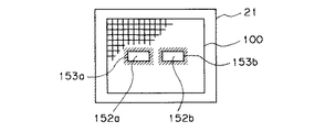
このように被写体光束は、上述した経路をたどって焦点検出光学系30に入射することになるが、焦点検出光学系30に入射した被写体光束は、視野マスク31・フィールドレンズ32・瞳マスク34(の二つの開口部34a・34b)及び再結像レンズ35(二つのレンズ35a・35b)を通過した後、CCD21の受光面となる撮像領域100上の所定の受光領域152a・152bに照射され、ここに像を再結像させることになる(図5参照)。
【0041】
この場合において(図2参照)、撮影光学系11により結像Iが結像面Gにおいて合焦状態で形成されている場合には、この結像Iは、フィールドレンズ32及び再結像レンズ35によってCCD21の撮像領域100上に再結像されることによって第1結像I1及び第2結像I2となる。なお、CCD21の撮像領域100は、光軸Oに対して垂直となる2次結像面である。
【0042】
また、撮影光学系11の状態が前ピン状態、即ち結像面Gの前方に被写体像Fが形成される場合には、この被写体像Fは、互いに光軸Oに近付いた位置において再結像されて、第1結像F1及び第2結像F2となる。
【0043】
そして、撮影光学系11の状態が後ピン状態、即ち結像面Gの後方に被写体像Rが形成される場合には、この被写体像Rは、互いに光軸Oから離間した位置において再結像されて、第1結像R1及び第2結像R2となる。
【0044】
つまり焦点検出光学系30は、上述のようにして被写体光束の一部を受けて二つの結像、即ち第1結像(I1・R1・F1)及び第2結像(I2・R2・F2)を、CCD21の受光面上に形成する。そして、それぞれの場合における第1結像及び第2像によるCCD21の出力を検出し、得られた信号に基づいて所定の処理を施すことで両者の間隔を検出し、よって撮影光学系11の状態、即ち合焦状態にあるか、前ピン状態又は後ピン状態にあるかを検出し得るようになっている。この場合の検出手段については、例えば第1結像と第2結像のそれぞれの光強度分布を、CCD21の対応する所定の領域152a・152b(図5参照)の各画像データ出力によって求め、両結像の間隔を測定する等、従来の焦点検出装置等において一般的に利用されている手段が採られる。
【0045】
なお、この場合において、撮影し得る全領域、即ちCCD21の撮像領域100の範囲は、例えばファインダー光学系により観察し得る撮影画面枠150(図4参照)に対応するようになっている。そして、この撮影画面枠150の範囲内における所定の領域、例えば略中央部に位置する領域に対応する被写体に対して焦点検出動作を行なうために、撮影画面枠150内に焦点検出領域151が設定される。
【0046】
上述したように焦点検出用の被写体光束は、メインミラー14のハーフミラー部を透過してサブミラー19によって焦点検出光学系30へと導かれる。したがって、メインミラー14のハーフミラー部及びサブミラー19の配置を任意に設定することにより、焦点検出領域151を所望の位置に設定することができるのである。
【0047】
そして、図5に示すように焦点検出光学系30は、視野マスク31によって規定される範囲内の所定の位置に視野マスク像153a・153bを結像させるのと同時に、この視野マスク像153a・153bの内部領域、即ち焦点検出用の所定の受光領域152a・152bに所定の像が再結像されることになる。このとき、制御回路(図1〜図5では図示せず;後述する図6のマイコン61参照。)は、CCD21からの出力信号、即ち所定範囲の画像データを受けて、これに基づいた焦点検出演算を実行することになる。
【0048】
なお、視野マスク像153a・153bは、CCD21に対して斜め下方側から照射され、CCD21の受光面上に再結像されることになるので、図5に示すように上部が若干開いた台形状の像となる。この場合においては、受光領域152a・152bに再結像される像もまた同様に変形することになるが、瞳分割方向(撮影画面の長辺に沿う方向)に対しては、略垂直方向となる変形であるので、焦点検出用の受光領域152a・152bの対称相似性に対する影響は非常に小さい。したがって、焦点状態の検出精度に対する影響はほとんどない。
【0049】
次に、図6は、本電子的撮像装置において主要となる電気的な構成部材を示すブロック構成図である。
【0050】
本電子的撮像装置は、中央処理装置(以下、CPUという)61a等からなる制御手段であるマイコン61によって全体が制御されるようになっている。即ち、このマイコン61は、本電子的撮像装置システムの制御装置であって、その内部にCPU61aと、ROM61bと、RAM61cと、A/Dコンバータ(ADC)61dと、内部メモリであるEEPROM61e等を有して構成されるコントローラである。そして、このマイコン61は、自己の内部に設けられるROM61bに予め格納されているシーケンスプログラムに従って本電子的撮像装置の一連の動作を制御するようになっている。
【0051】
また、EEPROM61eには、焦点調節演算や測光及び露出演算、AWB(オートホワイトバランス)演算等に関する各電子的撮像装置に固有の補正データが予め記憶されている。
【0052】
マイコン61には、絞り部材11b(図1参照)を駆動制御する絞り駆動部63と、合焦レンズ11a(図1参照)等を駆動制御するレンズ駆動部62と、各種の操作部材(図示せず)に連動し各種の指令信号を発生させるスイッチ群、例えば撮影動作を開始させるに際して測光及びAF動作等の予備的な動作を実行させる旨の指令信号を発生させるファーストレリーズスイッチ(1RSW)47、絞り部材11b等を駆動させて露出動作を実行させる旨の指令信号を発生させるセカンドレリーズスイッチ(2RSW)48等が電気的に接続されている。
なお、1RSW47と2RSW48とは、単一の操作部材によって操作し得るように構成されるいわゆる二段スイッチの形態となっている。
【0053】
また、マイコン61には、図7の要部ブロック構成図に示すようにタイミングジェネレータ(以下、TGという)82及びシグナルジェネレータ(以下、SGという)83等によって構成され、CCD21を駆動制御する撮像素子(CCD)制御部43が電気的に接続されている。そして、このCCD制御部43には、CCD21が電気的に接続されており、同CCD21の駆動を制御するようになっている。
【0054】
CCD21は、撮影光学系11を透過した被写体光束により形成される光学的な被写体像を電気信号に変換するものである。このCCD21の詳細な構成については後述する(図8・図9参照)。
【0055】
CCD21には、映像信号処理部42が電気的に接続されている。この映像信号処理部42は、CCD21からの出力信号を受けて所定の処理を施すことで、所定の形態の画像信号を生成するものである。この映像信号処理部42には、焦点検出演算部50、測光・露出演算部45、AWB部51、表示部46・記録部44等が電気的に接続されている。そして、この映像信号処理部42は、それぞれの構成ブロックに対して最適な形態の画像信号とこれに付随する情報等を生成し出力するようになっている。
【0056】
焦点検出演算部50は、映像信号処理部42からの出力信号を受けて焦点位置を検出し演算する焦点検出部を構成する回路であって、その演算結果や合焦状態の判定データ及び合焦レンズ11aの所定の駆動量データ等は、マイコン61へと出力されるようになっている。
【0057】
測光・露出演算部45は、映像信号処理部42からの出力信号を受けて被写体の輝度等を検出し最適となる露出データ、即ち絞り部材11bの絞り値及びCCD21の電子シャッター速度値等を算出する回路であって、その演算結果は、マイコン61へと出力されるようになっている。そして、これを受けてマイコン61は、絞り駆動部63を介して所定の絞り値となるように絞り部材11bを駆動すると共に、CCD制御部43を介して所定の電子シャッター速度値でCCD21を駆動制御することになる。
【0058】
AWB部51は、映像信号処理部42からの出力信号を受けて被写体のホワイトバランスが最適となるように自動的に調整するための回路であって、このAWB部51によって最適に調整された画像信号は、表示部46へと出力されるようになっている。
【0059】
表示部46は、例えば液晶ディスプレイ(LCD)等の画像表示装置によって形成され、映像信号処理部42及びAWB部51を介して入力される画像信号を画像として表示し得ると共に、その画像信号に付随する撮影情報等や撮影モード等の電子的撮像装置自体の内部情報等を文字や記号等の形態で視覚的に表示するものである。
【0060】
記録部44は、映像信号処理部42からの出力信号を受けて画像信号及びそれに付随する撮影情報等(以下、単に画像信号等という)を所定の形態で記録するものである。
【0061】
ここで、映像信号処理部42及び記録部44、CCD制御部43についての詳細な構成を、以下に説明する。
図7は、本電子的撮像装置における映像信号処理部42及び記録部44とこれらに対して電気的に接続される主要な電気回路の一部を取り出して示す要部ブロック構成図である。
【0062】
映像信号処理部42は、CCD21により取得される画像信号からリセットノイズ等を除去する相関二重サンプリング回路(以下、CDSという)78と、この相関二重サンプリング回路78の出力を増幅させるゲインコントロールアンプ(以下、AMPという)79と、AMP79の出力(アナログ信号)を受けてこれをデジタル信号に変換するADコンバータ(以下、A/Dという)80と、A/D80によりデジタル信号に変換された画像信号に対して所定の処理を行なうプロセス処理回路81等によって構成されている。
【0063】
CCD制御部43は、上述したようにCCD21に対して駆動信号を出力することで所定の動作を制御するものであって、次のような構成からなる。
即ち、CCD制御部43は、TG82SG83等によって構成されており、このうちTG82は、CCD21を駆動するための転送パルス等の駆動信号を発生させると共に、映像信号処理部42の相関二重サンプリング回路78のサンプルホールドパルス及びA/Dコンバータ80のAD変換タイミングパルス等を発生させるものである。
【0064】
またSG83は、TG82とマイコン61との間の同期をとるための信号を発生させるものである。
そして、CCD制御部43は、マイコン61の指令により測光・露出演算部45の演算結果に基づいて露出時におけるCCD21の電子シャッター、即ち露光時間を制御する役目をしている。
【0065】
記録部44は、上述したように映像信号処理部42からの出力信号を受けて画像信号等を所定の形態の画像データファイルとして、記録媒体86に格納し得るように構成されているものである。
【0066】
即ち、記録部44は、映像信号処理部42のプロセス処理回路81から出力される画像信号等を受けて、これを一時的に記憶する一時メモリであるDRAM84と、同画像信号等を画像データファイルとして所定の領域に格納し保存する記録媒体86と、DRAM84を介して入力された画像信号等を画像データファイルとして記録媒体86に記録するのに最適となる信号処理、つまり圧縮処理等を施すと共に、記録媒体86に記録された画像データファイルを読み出して再生表示をするのに最適となる信号処理を施す伸長回路等からなる圧縮伸長回路85等によって構成されている。
【0067】
次に、本電子的撮像装置の撮像素子(CCD)21の詳細な構成について、以下に説明する。図8は、本電子的撮像装置における撮像素子(CCD)の一部を拡大して示す要部拡大構成図である。
【0068】
本電子的撮像装置に適用されるCCD21の電荷転送タイプは、インターライン転送型である。CCD21の受光面には、撮像部となる複数の受光素子が水平方向と垂直方向に二次元的に並べて配置されており、これら個々の受光素子がそれぞれ一つの画素を形成するように構成されている。
【0069】
このCCD21は、水平方向と垂直方向に二次元的に配置された受光素子群であるフォトダイオード101と、このフォトダイオード101に蓄積された電荷(第1映像信号)を垂直シフトレジスタ103に転送するトランスファーゲート102と、転送された電荷を順次垂直方向に転送する垂直シフトレジスタ103と、垂直シフトレジスタ103により垂直方向に転送された電荷を水平方向に順次転送する水平シフトレジスタ104と、この水平シフトレジスタ104により水平方向に転送された電荷を電圧信号に変換して出力する出力部105等によって構成されている。
【0070】
また、フォトダイオード101の前面、即ち受光面となる側の面には、それぞれに所定の曲率を有し所定の焦点距離を有する球面レンズによって形成されるマイクロレンズアレイ(図示せず)が配置されている。このマイクロレンズアレイは、CCD21の光感度を向上させるために、各受光素子毎に対応させて配置されている。
【0071】
このように各受光素子の前面、即ち光束の入射面側にマイクロレンズアレイを設けることで、入射光を効率よく集光するようにしている。このような構成のものは、一般的に実用化されている手段であって、いわゆるオンチップマイクロレンズと呼ばれているものである。
【0072】
さらに、フォトダイオード101の前面側には、色フイルター(図8では図示せず。図9参照)が配置されている。この色フイルターの配列は、図9に示すようにいわゆるベイヤー配列となっている。なお、図9において示す符号R・G・Bは、それぞれ赤・緑・青を選択的に透過する色フイルター要素を示している。
【0073】
このように構成された本実施形態の電子的撮像装置における作用を、以下に説明する。図10は、本電子的撮像装置における制御手段であるマイコン61のメインルーチンを示すフローチャートである。また、図11は、本電子的撮像装置において撮像動作が実行される際のタイムチャートを示している。
【0074】
本電子的撮像装置は、例えば主電源スイッチ(図示せず)のオン操作により、又は電池の挿入操作等によってマイコン61を含む電気回路への給電が開始されることにより起動し、これによってマイコン61の内部のROM61bに予め格納されているシーケンスプログラムが実行される。
この状態において、まずステップS101では、本電子的撮像装置の各電気回路ブロックの初期化が行なわれる。
【0075】
次に、ステップS102において、マイコン61は、1RSW47の状態を検出し、これがオン状態にされたか否かの確認を行なう。ここで、所定の操作部材(図示せず)が操作されることによって生じる1RSW47のオン信号が確認された場合には、ステップS103の処理に進む。
【0076】
また、同1RSW47のオン信号が確認されなかった場合には、ステップS105の処理に進む。このステップS105においては、CCD21の撮像部である受光素子の蓄積動作及び読出動作等の一連の測光のための動作(以下、単に測光動作という)が行なわれて、次のステップS106の処理に進む。
【0077】
次いでステップS106においては、映像信号処理部42から出力されるCCD21により取得された画像信号を受けて測光・露出演算部45が、所定の測光及び露出演算処理を実行する。これにより、本露光動作時(画像記録を行なう際)必要となる情報、即ち被写体に応じた適正となる露出情報、例えば絞り部材11bの絞り値やCCD21の電子シャッター速度値等を算出する。
【0078】
つまり、本電子的撮像装置が起動されると測光動作が開始され、この測光動作は繰り返し実行されることになる(図11の符号[2]参照)。このとき図11の符号[3]に示すように絞り部材11bは、開放状態にある。
【0079】
一方、上述のステップS102において、1RSW47がオン状態にされたことを確認した場合には(図11の符号[1]参照)、次のステップS103において、CCD21を用いた焦点検出動作が実行される。この場合においては、上述したように撮影光学系11を透過した被写体光束は、メインミラー14及びサブミラー19を介して焦点検出光学系30に導かれている。そして、この焦点検出光学系30を介してCCD21の撮像領域100における所定の受光領域152a・152bに所定の像が結像されている。
【0080】
したがって、このステップS103では、CCD21における受光領域152a・152b内の蓄積動作(AF用露光。図11の符号[4]参照。詳細は図12によって後述する。)が実行される。これにより取得された焦点検出用の画像信号は、CCD21から映像信号処理部42を介して焦点検出演算部50へと出力され(読出動作)、次のステップS104において、その出力信号に基づいて焦点検出演算部50が所定の焦点検出演算を実行する(図11の符号[5]参照)。なお、ここで実行される所定の焦点検出演算についての詳細は後述する(図13参照)。
【0081】
次いで、ステップS107においては、上述のステップS104において実行した焦点検出演算の結果が合焦状態にあるか非合焦状態にあるかの判別を行なう。ここで、合焦状態であると判別された場合には、ステップS109の処理に移行し、また非合焦状態であると判別された場合には、ステップS108の処理に移行する。
【0082】
ステップS108において、上述のステップS104における焦点検出演算結果に基づいて合焦状態とするための合焦レンズ11aの移動量が算出されると共に、その算出結果に基づいてマイコン61は、レンズ駆動部62を駆動制御して合焦レンズ11aを移動させる(図11の符号[7]参照)。その後、ステップS102の処理に戻り、以降同様のAF動作の処理を繰り返す。
【0083】
一方、ステップS109においては、2RSW48の状態を検出しオン状態となっているか否かの確認を行なう。ここで、2RSW48がオン状態であることが確認された場合(図11の符号[6]参照)には、次のステップS110の処理に進み、同2RSW48がオフ状態であることが確認された場合には、ステップS102の処理に戻り、2RSW48がオン状態になるのを待機しながら、以降のシーケンスを継続して実行する。
【0084】
ステップS110以降の処理において、いわゆる本露光動作(図11の符号[8]参照)が実行される。
この本露光動作は、まずステップS110において、マイコン61が絞り駆動部63を介して絞り部材11bを制御し、これにより上述のステップS106において算出した露出用絞り値となるように駆動する(絞り制御処理;図11の符号[9]参照)。
【0085】
次いでステップS111において、CCD制御部43は、CCD21を制御して、電荷掃き出し信号(SUB。図11参照)をオフ状態に切り換えてCCD21による蓄積動作を開始させ、上述のステップS106における露出演算処理によって算出した電子シャッター速度値により本露光動作を実行する(図11の符号[8]参照)。ここで、電子シャッターとは、CCD制御部43により算出された電子シャッター速度値に応じた所定のタイミングで電荷転送パルス(TGP。図11参照)を発生させて、フォトダイオード101の蓄積電荷を垂直シフトレジスタ103へと転送する動作である。
【0086】
そして、次のステップS112においては、取得されるべき画像信号に対していわゆるスミア等のノイズ成分が混入するのを防止するために、絞り駆動部63を介して絞り部材11bが閉状態となる方向に駆動され、同絞り部材11bは完全に遮閉状態となる(図11の符号[10]参照)。これによってCCD21の受光面が遮光状態となる。
【0087】
続いてステップS113においては、CCD21の遮光状態を保持したまま、CCD制御部43が画像読み出し信号(DCLK。図11参照)をCCD21へと出力する。そして、映像信号処理部42は、同信号(DCLK)に同期して出力されるCCD21の信号(CCD信号;画素信号。図11参照)をA/D変換した後、これを読み出す(図11の符号[11]参照)。
【0088】
次いで、ステップS114において、マイコン61は、絞り駆動部63を介して絞り部材11bを開放状態にするべく、所定の絞り開放コマンドを送信し、同絞り部材11bを駆動し、これを開放状態に戻す(図11の符号[12]参照)。
【0089】
さらに、ステップS115において、映像信号処理部42は、CCD21によって取得された画像信号を記録するのに最適な形態とする所定の処理、例えば圧縮処理等を行なった後、これを記録媒体86の所定の領域に格納する(図11の符号[12]参照)。その後、一連の動作を終了して、上述のステップS102の処理に戻り、以降の処理を同様に繰り返す。
【0090】
次に、本電子的撮像装置において、焦点検出動作を行なう際に撮像素子(CCD)によって実行される焦点検出用の蓄積動作(AF用露光)及び焦点検出演算の手順について、図12・図13のフローチャートを用いて説明する。
【0091】
図12は、本電子的撮像装置における撮像素子(CCD)の焦点検出用の受光領域における蓄積動作及び読出動作のシーケンスを示すフローチャートである。また、図13は、焦点検出演算のシーケンスを示すフローチャートである。
【0092】
なお、図12に示されるシーケンスは、図10のステップS103の処理に相当するものであり、また図13に示されるシーケンスは、図10のステップS104の処理に相当するものであって、これらを詳述するものである。
【0093】
まず、図12を用いて焦点検出用の受光領域における蓄積動作及び読出動作のシーケンスを説明する。
まずステップS200では、本電子的撮像装置におけるCCD21の撮像領域100のうち焦点検出用の受光領域152a・152bに関する情報、即ち受光領域152a・152bの有効画素範囲に関する情報をマイコン61のEEPROM61eより読み出す。
【0094】
この受光領域152a・152bの有効画素範囲に関する情報は、個々の電子的撮像装置に適用されるCCD21毎に異なる固有の情報である。したがって、電子的撮像装置の製造時において、予め個々の電子的撮像装置毎に固有の情報の確認がなされており、各電子的撮像装置に応じた適切な情報が各電子的撮像装置のマイコン61内に設けられるEEPROM61eに予め記憶されている。
【0095】
次に、ステップS201において、前回行なわれた蓄積動作によって得られている受光領域152a・152bにおける画素信号を参照し、適正な画素信号が得られるような蓄積時間を算出し決定する。
【0096】
ステップS202においては、上述のステップS201において算出された蓄積時間に基づいて、マイコン61は、CCD制御部43を介してCCD21の蓄積動作を制御する。
【0097】
ステップS203においては、CCD21の出力、即ち画素信号の読み出し動作を実行する。この焦点検出動作を行なうに際しては、撮像領域100の受光領域152a・152b以外の領域の画素信号は、使用しないことにしていることから、いわゆる高速掃き出し動作を行なって読み出し時間を短縮するようにしている。
【0098】
そして、次のステップS204において、上述のステップS200の処理でEEPROM61eから読み出した有効画素範囲の情報に基づき受光領域152a・152bに対応する領域の画素信号のみを読み出した後、図10のメインルーチンに復帰する。
【0099】
なお、このような焦点検出演算の他に、本電子的撮像装置では、CCD21を利用して測光・露出演算やAWB演算等を行なうようにしている。この場合には、上述したような高速掃き出し処理を行なわずに撮像領域100の全領域を利用するようにしたり、焦点検出演算処理と同様に測光・露出演算処理を行なうための所定の領域やAWB演算を行なうための所定の領域等に応じた領域の画素信号を読み出すようにすれば良い。この場合には、各所定の領域に関する情報を予めEEPROM61e等に記憶させておき、各演算を実行する前に対応する情報を読み込ませる等の処理を行なうようにすれば良い。そして、CCD21の撮像領域100のうちの各所定の領域に対して、所定の手段、例えばメインミラー14の全体をハーフミラーで形成する等の手段によって必要となる被写体光束を導くようにする必要がある。
【0100】
次に、上述のようにして取得した焦点検出用の受光領域152a・152bの画素信号に基づいて焦点検出演算を行なう際のシーケンスを、図13によって説明する。
【0101】
本電子的撮像装置において実行される焦点検出演算処理は、従来より公知のTTL位相差検出方式が用いられる。したがって、その詳細な説明は省略し、本実施形態における特徴となる部分についてのみ、以下に詳述する。
【0102】
焦点検出演算のシーケンス(図10のステップS104及び図13参照)に移行すると、まずステップS300では、焦点検出領域内、即ち受光領域152a・152bの同色信号を列方向に加算する。
【0103】
即ち、CCD21の焦点検出用の受光領域152a・152bのうち図14の符号Xで示す瞳分割方向に対して直交する方向となる列方向の同色の画素信号をそれぞれ加算処理する。この加算処理は、R・G・Bのそれぞれの色要素について行なわれる。なお、図14は、焦点検出演算が行なわれる際の加算処理を概念化して示す図である。
【0104】
ここで行なわれる加算処理は、次のように行われることになる。
図14に示すようにCCD21の焦点検出用の受光領域152aにおいて、第一列目の同色信号のうちR信号を加算処理して得られたデータがR1Lであり、G信号を加算処理して得られたデータがG1Lである。同様に第二列目の同色信号のうちのG信号を加算処理して得られたデータがG2Lであり、B信号を加算処理して得られたデータがB1Lである。
【0105】
また、同様にしてCCD21の焦点検出用の受光領域152bにおいても同様の加算処理を行なって所定のデータを取得する。そして、このようにして得られるデータは、G信号については、受光領域152aの側でG1L・G2L・G3L…が、受光領域152bの側でG1R・G2R・G3R…がそれぞれ得られる。同様にR信号については、受光領域152aの側でR1L・R2L・R3L…が、受光領域152bの側でR1R・R2R・R3R…が得られ、B信号については、受光領域152aの側でB1L・B2L…が、受光領域152bの側でB1R・B2R…が得られる。
【0106】
次に、ステップS301では、上述のステップS300において取得した同色加算信号の各データを用いて一般的な位相差検出演算をR・G・Bの各色要素毎に行なう。
【0107】
例えば、受光領域152a側の加算後データG1L・G2L・G3L…と、受光領域152b側の加算後データG1R・G2R・G3R…とによって位相差検出演算を行なう。
【0108】
そして、次のステップS302では、上述のステップS301における位相差検出演算の信頼性についてそれぞれ評価して、焦点検出が可能であるか否かの判定を行なう。
【0109】
ステップS303では、信頼性があり焦点検出が可能であると判定された演算結果を選択して平均処理を行なう。
【0110】
次いで、ステップS304において、上述の演算結果からデフォーカス量を算出した後、図10のメインルーチンに復帰する(リターン)。
【0111】
以上説明したように上記第1の実施形態によれば、メインミラー14の一部にハーフミラー部を設け、このハーフミラー部を透過した被写体光束をサブミラー19によって焦点検出光学系30へと導くようにし、この焦点検出光学系30を介して被写体光束をCCD21の撮像領域100のうちの所定の受光領域152a・152bに対して照射するようにし、これによって焦点検出動作を実行するようにしている。
【0112】
つまり、焦点検出動作を行なうための専用の撮像手段を特に配設することなく、被写体光束の一部を撮像用の撮像手段の所定の位置へと導くことにより、この撮像用の撮像手段を利用した焦点検出動作を実行するようにしている。したがって、電子的撮像装置の構成部材数を低減化することができ、よって装置の小型化に寄与し得ると共に、装置全体の製造コストの低減化に寄与することができる。
【0113】
なお、上述の第1の実施形態の電子的撮像装置において行なわれる焦点検出演算処理については、次に示すような手段としてもよい。
【0114】
図15は、上記第1の実施形態の電子的撮像装置において行なわれる焦点検出演算の加算処理の変形例を示す概念図である。
【0115】
この変形例においては、焦点検出用の受光領域152a・152bにより取得され得る画素信号のうち所定の信号のみを取り出すようにしたいわゆる間引き読み出しを行なう場合の例を示すものである。
【0116】
即ち、図15に示すように例えば焦点検出領域内、即ち受光領域152a・152bの同色信号を列方向に加算する。この場合において、列方向の同色信号のうち三つ毎に一つの画素信号を取得する間引き読み出しを行なって、読み出した画素信号については、垂直シフトレジスタ103の内部において加算処理を行なう。
【0117】
この間引き読み出しについては、例えば本出願人が先に特開平10−136244号公報等によって開示しているように、撮像素子としてCCDを適用している場合には、読み出しクロックの操作を行なうことによって垂直シフトレジスタ103の動作を制御することで容易に実現することができるものである。
【0118】
なお、図15では、一方の受光領域152aのみについて図示しているが、他方の受光領域152bについても全く同様に処理されることになる。
【0119】
このように、列方向に所定の数置きに画素信号を読み出すようにすることで、全体的な画素信号の読み出し時間を短縮化することができると共に、演算処理のために扱う画素信号量が減ることになるので、演算速度を高速化することが容易となる。したがって、焦点検出動作のより一層の高速化を実現することができる。
【0120】
また、図16は、上記第1の実施形態の電子的撮像装置において行なわれる焦点検出演算の加算処理の別の変形例を示す概念図である。
【0121】
この図16に示される別の変形例では、図15の場合と同様に焦点検出用の受光領域152a・152bにより取得され得る画素信号のうち所定の信号のみを取り出すようにした間引き読み出しを行なう場合の異なる例を示している。
【0122】
この場合には、上述の変形例と同様に列方向の同色信号のうち所定の画素信号、即ち三つ毎に二つの画素信号を取得する間引き読み出しを行なっている。このようにして読み出した画素信号については、垂直シフトレジスタ103の内部において、上述の第1の実施形態やその変形例と同様の加算処理を行なう。
【0123】
このような処理を行なうことで、上述の変形例と同様に読み出し時間の高速化及び読み出す画素信号量の削減化による演算速度の高速化を図ることができる。
【0124】
次に、本発明の第2の実施形態について、以下に説明する。
図17は、本発明の第2の実施形態の電子的撮像装置における主要構成部材の配置を概略的に示す図であって、合わせて撮影光学系を透過した光束の本電子的撮像装置の内部における光路を示している。この図17は、上述の第1の実施形態における図1に相当する図であって、図1と同様に、図面の繁雑化を避けるために、本発明に関連しない構成部材については、その図示を省略し、本発明の関連する構成部材のみを示すようにしている。
【0125】
本実施形態の電子的撮像装置の構成は、基本的に上述の第1の実施形態と略同様であり、焦点検出光学系の構成が異なるのみである。
即ち、本実施形態の焦点検出光学系130は、図17に示すように視野マスク131・フィールドレンズ132・全反射ミラー133・全反射ミラー136・瞳マスク134・再結像レンズ135等によって構成されている。この焦点検出光学系130の基本的な構成の概念は、上述の第1の実施形態と全く同様である(図2・図3参照)。
【0126】
なお、本実施形態においては、焦点検出光学系130から出射した焦点検出用の光束をCCD21の撮像領域の所定の位置に導くために、サブミラー19の後方に、さらに全反射ミラー137を配置している。この全反射ミラー137は、焦点検出光学系130からの焦点検出用の光束を反射させることによって、その光路を折り曲げて、下方に位置する焦点検出光学系130からの光束を、本電子的撮像装置の後方に配置されるCCD21の側へと導き、その受光面上に再結像させるために設けられているものである。
【0127】
そして、本電子的撮像装置においても撮影動作時には、メインミラー14及びサブミラー19が撮影位置(図17の点線位置)に退避することになるが、このとき同時に全反射ミラー137も被写体光束を遮らない位置、即ち図17の点線で示す位置へと所定の移動機構(図示せず)によって移動し、これによって被写体光束の光路上から退避するようになっている。
【0128】
このような構成の焦点検出光学系130とした場合には、CCD21に対して略垂直に焦点検出用の光束を入射させて、撮像領域100の所定の位置に焦点検出用の像を再結像させるようにしている。この場合のCCD21における撮像領域100に結像される視野マスク像153a・153b及び焦点検出用の受光領域152a・152bは、図17のように上述の第1の実施形態において生じる変形は生じない。
【0129】
その他の構成については、上述の第1の実施形態の電子的撮像装置と略同様に構成されており、その作用についても同様である。
なお、本実施形態においては、上述したように撮影動作時には、メインミラー14及びサブミラー19が被写体光束の光路外に退避するのと同時に、全反射ミラー137も図示しない移動機構によって被写体光束の光路外に退避する。これによって、撮影光学系11を透過した被写体光束の全てがCCD21の受光面の撮像領域100に照射することになる。
【0130】
以上説明したように上記第2の実施形態によれば、上述の第1の実施形態と同様の効果を得ることができると共に、上述の第1の実施形態の電子的撮像装置における焦点検出光学系30によって発生する像の変形(図5参照)等の問題を解消することができ、よって焦点検出精度をより向上させることができる。
【0131】
次に、本発明の第3の実施形態について、以下に説明する。
図19は、本発明の第3の実施形態の電子的撮像装置における主要構成部材の配置を概略的に示す図であって、合わせて撮影光学系を透過した光束の本電子的撮像装置の内部における光路を示している。また、図20は、本電子的撮像装置における焦点検出光学系の構成の概念を示す斜視図であって、合わせて撮影光学系を透過した被写体光束が焦点検出光学系230を介してCCD21へと到達する際の様子を概念的に示す図である。
【0132】
なお、図19は、上述の第1の実施形態における図1に相当する図であり、図20は、同様に第1の実施形態における図3に相当する図である。これら図19・図20は、図面の繁雑化を避けるために、本発明に関連しない構成部材については、その図示を省略し、本発明の関連する構成部材のみを示すものである。
【0133】
本実施形態の電子的撮像装置の構成は、基本的に上述の第1の実施形態と略同様であるが、焦点検出光学系の構成が異なると共に、CCD21の全面にフォーカルプレーンシャッターを配置している点が異なる。
【0134】
即ち、本実施形態の焦点検出光学系230は、図19に示すようにフィールドミラー232・瞳マスク234・再結像レンズ235等によって構成されている。フィールドミラー232は、凹面の内側に反射面を有する反射鏡により形成されている。そして、このフィールドミラー232は、上述の第1の実施形態の電子的撮像装置における焦点検出光学系30を構成する視野マスク31・フィールドレンズ32・全反射ミラー33の機能を一部材によって実現しているものである。
【0135】
つまり、フィールドミラー232は、撮影光学系11(図20では図示せず)を透過した被写体光束であって、サブミラー19(図20では図示せず)からの光束のうち一部の光束のみが反射し得るように、その反射面Aの側の略中央部近傍に所定の範囲の反射部232aが設けられている。
【0136】
また、フィールドミラー232は、上述したように凹面の内側に反射面Aを有する反射鏡によって形成されていることから、上記反射部232aによって集光された所定の光束のみが反射するようになっている。したがって、光束の光路は、これによって変換されてCCD21の側に導かれるようになっている。こうしてフィールドミラー232は、第1の実施形態における焦点検出光学系30の視野マスク31・フィールドレンズ32・全反射ミラー33の機能を一部材で実現している。
【0137】
そして、フィールドミラー232により反射された光束は、二つの開口部234a・234bを有する瞳マスク234及び二つのレンズ235a・235bからなる再結像レンズ235を介して焦点検出光学系230から出射することになる。
【0138】
このようにして焦点検出光学系230から出射した焦点検出用の光束は、図20に示すようにCCD21の受光面の撮像領域100の所定の受光領域152a・152bへと入射するようになっている。
【0139】
一方、CCD21の前面側には、機械式のシャッター機構であるフォーカルプレーンシャッター22が配置されている。このフォーカルプレーンシャッター22は、一般的な一眼レフレックスカメラ等に適用されているものと同様の構成、即ち先幕23及び後幕24等からなり、先幕23と後幕24との間に形成されるスリットによって、露光動作を行なうようにしたものである。
【0140】
そして、フォーカルプレーンシャッター22は、焦点検出動作が行なわれる場合、即ち電子的撮像装置が撮影準備状態にあるときには、メインミラー14が図19の実線で示す位置にあると共に、先幕23が開放状態となる位置に配置されるようになっている。これにより、焦点検出用の光束のみがCCD21の撮像領域100(図20参照)の所定の受光領域152a・152bに入射するように構成されている。
【0141】
即ち、この状態においては、CCD21の撮像領域100の所定の受光領域152a・152b以外の部分への入射光は、上述の第1の実施形態と同様にメインミラー14の全反射ミラー部、即ちサブミラー19に対応するハーフミラー部以外の領域により遮光されるようになっている。したがって、焦点検出動作が行なわれるときには、焦点検出用の光束のみがCCD21の撮像領域100(図20参照)の所定の受光領域152a・152bに入射することになる。
【0142】
一方、撮影動作が行われるときには、メインミラー14及びサブミラー19が図19の点線で示す位置(撮影位置)に退避すると共に、フォーカルプレーンシャッター22は、機械的チャージ機構(図示せず)の作用によってチャージされ、先幕23がセット状態になる。
【0143】
そして、測光・露出演算部45による演算処理の結果、算出されたシャッタ秒時の情報に基づいて先幕23及び後幕24の駆動制御が行なわれ、これによって本露光動作が実行されることになる。
【0144】
また、上述の第1の実施形態の電子的撮像装置においては、本露光動作後に行なわれるCCD21の画素データ読み出し時に、絞り部材11bを完全な遮閉状態とすることでCCD21への光束を遮光するようにしているが、本実施形態においては、CCD21の全面に配置したフォーカルプレーンシャッター22によってCCD21の遮光状態を保持し得るので、絞り部材11bは、絞り開口を保持し撮影光学系11への入射光束を規制する絞り機能の役目をするのみである。
【0145】
その他の構成については、上述の第1の実施形態の電子的撮像装置と略同様の構成となっており、その作用は、上述のフォーカルプレーンシャッター22の作用が加わる一方、絞り部材11bによる遮光動作が不要となる点以外は、上述の第1の実施形態と同様である。
【0146】
以上説明したように上記第3の実施形態によれば、上述の第1の実施形態と同様の効果を得ることができることに加え、本実施形態の電子的撮像装置における焦点検出光学系230では、第1の実施形態の電子的撮像装置の焦点検出光学系30における視野マスク31・フィールドレンズ32・全反射ミラー33によって実現される機能を、フィールドミラー232の一部材によって機能するようにしているので、焦点検出光学系230を構成する部材数を削減すると同時に、その構成の簡易化を実現している。したがって、電子的撮像装置全体の製造コストのさらなる低減化に寄与することができる。
【0147】
また、本露光動作後に行なわれるCCD21の画素データ読み出し時には、CCD21の全面に配置したフォーカルプレーンシャッター22によってCCD21の遮光状態を保持するようにしているので、絞り部材11bは、絞り開口を保持し撮影光学系11への入射光束を規制するのみの動作を行なえば良い。したがって絞り部材11bを駆動制御する絞り駆動部63の制御シーケンスをより単純化することができる。
【0148】
次に、本発明の第4の実施形態について、以下に説明する。
図21は、本発明の第4の実施形態の電子的撮像装置における主要構成部材の配置を概略的に示す図であって、合わせて撮影光学系を透過した光束の本電子的撮像装置の内部における光路を示している。また、図22は、本電子的撮像装置における焦点検出光学系の構成の概念を示す斜視図であって、合わせて撮影光学系を透過した被写体光束が焦点検出光学系330を介してCCD21へと到達する際の様子を概念的に示す図である。
【0149】
なお、図21は、上述の第1の実施形態における図1に相当する図であり、図22は、第1の実施形態における図3に相当する図である。これら図21・図22においては、図面の繁雑化を避けるために、本発明に関連しない構成部材については、その図示を省略し、本発明の関連する構成部材のみを示すものである。
【0150】
本実施形態の電子的撮像装置の構成は、基本的に上述の第1の実施形態と略同様であるが、焦点検出光学系の構成が異なるものである。
【0151】
即ち、本実施形態の焦点検出光学系330は、図21に示すように視野マスク331・フィールドレンズ332・第1全反射ミラー333及び第2全反射ミラー336・再結像ミラー335等によって構成されている。
【0152】
再結像ミラー335は、凹面形状からなり内側に全反射面を有する二つの反射鏡であるミラー335a・335bによって構成されている。この再結像ミラー335は、上述の第1の実施形態の電子的撮像装置における焦点検出光学系30の一部を構成する瞳マスク34及び再結像レンズ35の機能を合わせて備えたものである。
【0153】
つまり、再結像ミラー335の二つのミラー335a・335bの各反射面には、上述の第3の実施形態における焦点検出光学系230のフィールドミラー232と同様に、入射する光束のうち一部の光束のみが反射するように、反射面の略中央部近傍に所定の範囲の反射部が設けられている。したがって、これにより上述の第1の実施形態における焦点検出光学系30の瞳マスク34の機能を有している。また、これと同時に再結像ミラー335は、その凹面反射鏡による集光及び反射作用によって光束を集光し所定の像を再結像させる再結像レンズ35の機能をも有しているのである。
【0154】
その他の構成については、上述の第1の実施形態の電子的撮像装置と略同様の構成となっている。また、その作用についても略同様である。
【0155】
なお、本実施形態においては、焦点検出動作が行なわれる場合には、サブミラー19から焦点検出光学系330へと導かれた焦点検出用の光束の光路は、次のような経路をたどることになる。
【0156】
即ち、撮影光学系11を透過した被写体光束であって、サブミラー19からの焦点検出光学系330へと導かれた焦点検出用の光束は、まず視野マスク331によって所定量の光束に規制されて、これを通過した後、フィールドレンズ332によって集光され、第1全反射ミラー333の反射面によって反射する。これにより、その光路が変更されて、同光束は第2全反射ミラー336へと導かれる。そして、同光束は、第2全反射ミラー336によって再度反射することによって、その光路を変更して、再結像ミラー335へと導かれる。
【0157】
この再結像ミラー335の二つのミラー335a・335bに入射した各光束は、それぞれの反射面で反射して二つの像をCCD21の撮像領域100の所定の二つの受光領域152a・152bに照射され、ここに所定の像を再結像させる。そして、この二つの像に基づいて焦点検出動作が実行されることになる。
【0158】
その他の構成及び作用については、上述の第1の実施形態の電子的撮像装置と略同様である。
【0159】
以上説明したように上記第4の実施形態によれば、上述の第1の実施形態と同様の効果を得ることができる。
また、上述の第1の実施形態の電子的撮像装置の焦点検出光学系30においては、瞳マスク34の二つの開口部34a・34bを通過した光束を再結像レンズ35の二つのレンズ35a・35bによって再結像するようにしていたので、同レンズ35a・35bにより生ずる収差等の影響を受けて像の位置ずれ等の問題があった。
【0160】
しかし、本実施形態においては、上述の第1の実施形態の電子的撮像装置の焦点検出光学系30における瞳マスク34と再結像レンズ35との機能を再結像ミラー335によって実現するようにしたので、上述のような問題を解消することができる。したがって、これにより、さらに高精度な焦点検出動作を実現することが容易となる。
【0161】
[付記]
上記発明の実施形態により、以下のような構成の発明を得ることができる。
【0162】
(1) 撮影光学系を透過して結像される光学的な被写体像を光電変換することにより電気的な画像信号を生成する撮像素子を有してなる電子的撮像装置において、
上記撮影光学系を透過した被写体光束のうちの少なくとも一部を上記撮像素子の受光面に再結像させる焦点検出光学系と、
上記撮影光学系を透過した被写体光束のうちの少なくとも一部を上記焦点検出光学系へと導く光学部材と、
上記撮像素子の出力信号に基づいて焦点検出動作を実行する焦点検出部と、
を具備して構成されている電子的撮像装置。
【0163】
(2) 付記1に記載の電子的撮像装置において、
上記撮影光学系を透過した被写体光束を二つの光束に分割し、一方の光束を被写体観察用の光束としてファインダー光学系へと導くと共に、他方の光束を焦点検出用の光束として上記光学部材へと導く分割光学系を、さらに有して構成されている。
【0164】
(3) 付記2に記載の電子的撮像装置において、
上記分割光学系は、焦点検出動作の実行中には上記撮影光学系を透過した被写体光束の光路上に配置され、撮影動作の実行中には上記撮影光学系を透過した被写体光束の光路上から退避する位置に移動する。
【0165】
(4) 付記2に記載の電子的撮像装置において、
上記分割光学系は、クイックリターンミラーによって構成されている。
【0166】
(5) 付記2に記載の電子的撮像装置において、
上記分割光学系は、一部が半透過鏡により、他の一部は全反射鏡によって構成されている。
【0167】
(6) 付記2に記載の電子的撮像装置において、
上記光学部材は、全反射鏡により構成されている。
【0168】
【発明の効果】
以上述べたように本発明によれば、撮影光学系により結像された被写体像を撮像素子を利用して画像信号に光電変換し、この画像信号を画像データとして記録媒体に記録する電子的撮像装置において、焦点検出を行なうための専用の撮像素子が不要となるような構成を採ることで、装置自体の小型化及び製造コストの低減化に寄与し得る電子的撮像装置を提供することができる。
【図面の簡単な説明】
【図1】本発明の第1の実施形態の電子的撮像装置における主要構成部材の配置と、撮影光学系を透過した光束の電子的撮像装置の内部における光路とを合わせて示す図。
【図2】図1の電子的撮像装置における焦点検出光学系の構成を示す側断面図であって、合わせて撮影光学系を透過した被写体光束が焦点検出光学系を介して撮像素子へと到達する際の様子を概念的に示す図。
【図3】図1の電子的撮像装置における焦点検出光学系の構成を示す斜視図であって、合わせて撮影光学系を透過した被写体光束が焦点検出光学系を介して撮像素子へと到達する際の様子を概念的に示す図。
【図4】図1の電子的撮像装置における撮影画面内の焦点検出領域の配置を示す図。
【図5】図1の電子的撮像装置における撮影画面の焦点検出領域に対応する撮像素子(CCD)の受光部(撮像領域)の受光領域を示す概念図。
【図6】図1の電子的撮像装置において主要となる電気的な構成部材を示すブロック構成図。
【図7】図1の電子的撮像装置における映像信号処理部及び記録部とこれらに対して電気的に接続される主要な電気回路の一部を取り出して示す要部ブロック構成図。
【図8】図1の電子的撮像装置における撮像素子(CCD)の一部を拡大して示す要部拡大構成図。
【図9】図1の電子的撮像装置における撮像素子(CCD)の色フイルターの色要素を示す配列図。
【図10】図1の電子的撮像装置における制御手段(マイコン)のメインルーチンを示すフローチャート。
【図11】図1の電子的撮像装置において撮像動作が実行される際のタイムチャート。
【図12】図1の電子的撮像装置における撮像素子(CCD)の焦点検出用の受光領域における蓄積動作及び読出動作のシーケンスを示すフローチャート。
【図13】図1の電子的撮像装置において行なわれる焦点検出演算のシーケンスを示すフローチャート。
【図14】図1の電子的撮像装置において焦点検出演算が行なわれる際の加算処理を概念化して示す図。
【図15】本発明の第1の実施形態の電子的撮像装置において行なわれる焦点検出演算の加算処理の変形例を示す概念図。
【図16】本発明の第1の実施形態の電子的撮像装置において行なわれる焦点検出演算の加算処理の別の変形例を示す概念図。
【図17】本発明の第2の実施形態の電子的撮像装置における主要構成部材の配置と、撮影光学系を透過した光束の電子的撮像装置の内部における光路とを合わせて示す図。
【図18】図17の電子的撮像装置における撮影画面の焦点検出領域に対応する撮像素子(CCD)の受光部(撮像領域)の受光領域を示す概念図。
【図19】本発明の第3の実施形態の電子的撮像装置における主要構成部材の配置と、撮影光学系を透過した光束の電子的撮像装置の内部における光路とを合わせて示す図。
【図20】図19の電子的撮像装置における焦点検出光学系の構成を示す斜視図であって、合わせて撮影光学系を透過した被写体光束が焦点検出光学系を介して撮像素子へと到達する際の様子を概念的に示す図。
【図21】本発明の第4の実施形態の電子的撮像装置における主要構成部材の配置と、撮影光学系を透過した光束の電子的撮像装置の内部における光路とを合わせて示す図。
【図22】図21の電子的撮像装置における焦点検出光学系の構成を示す斜視図であって、合わせて撮影光学系を透過した被写体光束が焦点検出光学系を介して撮像素子へと到達する際の様子を概念的に示す図。
【符号の説明】
11……撮影光学系
11a……合焦レンズ(焦点調節光学系)
11b……絞り部材
12 フイルター
12……赤外光カットフイルター
13……光学的ローパスフイルター(LPF)
14……メインミラー
19……サブミラー
21……固体撮像素子(CCD)
22……フォーカルプレーンシャッター
30・130・230・330……焦点検出光学系
31・131・331……視野マスク(焦点検出光学系)
32・132・332……フィールドレンズ(焦点検出光学系)
33・133……全反射ミラー(焦点検出光学系)
34・134……瞳マスク(焦点検出光学系)
35・135……再結像レンズ(焦点検出光学系)
42……映像信号処理部
43……CCD制御部
44……記録部
45……測光・露出演算部
46……表示部
50……焦点検出演算部
51……AWB部
61……マイコン
62……レンズ駆動部
63……絞り駆動部
136 全反射ミラー(焦点検出光学系)
137 全反射ミラー(焦点検出光学系)
232 フィールドミラー(焦点検出光学系)
234 瞳マスク(焦点検出光学系)
235 再結像レンズ(焦点検出光学系)
333 第1全反射ミラー(焦点検出光学系)
335 再結像ミラー(焦点検出光学系)
336 第2全反射ミラー(焦点検出光学系)[0001]
BACKGROUND OF THE INVENTION
The present invention relates to an electronic image pickup apparatus, and more particularly to an electronic image pickup apparatus having an image pickup device that generates an electric image signal by photoelectrically converting an optical subject image formed by a photographing optical system. The present invention relates to an applied focus detection device.
[0002]
[Prior art]
In recent years, an optical subject image formed by a subject light beam that has passed through a photographing optical system is photoelectrically converted into an electrical signal using an imaging device such as a CCD (Charge Coupled Device), and the like. Various proposals have been made for electronic imaging devices such as digital still cameras and digital video cameras capable of recording the image signals generated by the above as image data in a predetermined form on a recording medium or the like.
[0003]
For example, Japanese Patent Application Laid-Open No. 8-262564 discloses that a subject image to be photographed and recorded using a light beam transmitted through a single photographing optical system and a subject image for observation can be formed at different positions. A single-lens reflex type electronic imaging apparatus configured as described above is disclosed. This electronic imaging apparatus is provided with imaging means such as a solid-state imaging element for imaging on the imaging plane of the subject image for imaging, and separately from the imaging means for imaging at a position equivalent to this imaging plane, An imaging means for focus detection is provided. Then, a TTL phase difference detection type focus detection means (AF means) for detecting the focus state of the subject image is configured by guiding a part of the light beam that has passed through the photographing optical system to the focus detection imaging means. Based on this, the focusing operation is performed.
[0004]
An electronic imaging apparatus disclosed in Japanese Patent Laid-Open No. 9-274130 is a so-called video movie camera that mainly captures and records moving images, and imaging means such as an imaging element for imaging is provided in the camera body. On the other hand, a focus detection unit of a TTL phase difference detection system configured by another imaging unit different from the imaging unit such as the imaging element for imaging is arranged inside a lens barrel for holding a photographing lens It is what you do.
[0005]
[Problems to be solved by the invention]
However, in the conventional electronic imaging device disclosed by the above-mentioned JP-A-8-262564, the above-mentioned JP-A-9-274130, etc., separately from imaging means such as an imaging element for photographing and recording a subject image, An imaging means such as a dedicated imaging element for performing focus detection is provided.
[0006]
In the case of such a configuration, there are problems that the number of parts of the entire electronic imaging device is increased and the size of the device itself is increased. At the same time, since a plurality of expensive parts such as an image sensor are required, there is a problem that the manufacturing cost is increased.
[0007]
The present invention has been made in view of the above-described points, and an object of the present invention is to photoelectrically convert a subject image formed by a photographing optical system into an image signal using an image pickup device, and this image. In an electronic imaging device that records a signal on a recording medium as image data, a configuration that eliminates the need for a dedicated imaging device for focus detection reduces the size of the device itself and reduces manufacturing costs. It is to provide an electronic imaging device that can contribute.
[0008]
[Means for Solving the Problems]
In order to achieve the above object, an electronic imaging apparatus according to an aspect of the present invention provides image data from an imaging lens, an observation optical system for observing an image formed by the imaging lens, and an image formed by the imaging lens. An image pickup device for generating, a focus detection optical system for forming two images on the image pickup device from a light beam that has passed through an exit pupil of the photographing lens, and the observation optical system and the focus when set to a photographing preparation position. The light beam of the photographic lens is guided to the detection optical system, and the distance between the two images is determined from the output signal of the image sensor at a mirror and a shooting preparation position of the mirror that guides the light beam to the image sensor when the photographing position is set. A focus adjustment circuit that detects and calculates a defocus amount for focus adjustment of the photographing lens.The mirror further includes a sub-mirror, and the sub-mirror guides the light beam from the photographing lens that has passed through the semi-transmissive portion of the mirror to the focus detection optical system.
[0011]
DETAILED DESCRIPTION OF THE INVENTION
The present invention will be described below with reference to the illustrated embodiments.
FIG. 1 is a diagram schematically showing the arrangement of main components in the electronic image pickup apparatus according to the first embodiment of the present invention. The optical path in is shown. In FIG. 1, in order to avoid complication of the drawing, the illustration of the structural members not directly related to the present invention is omitted, and only the structural members directly related to the present invention are shown.
[0012]
As shown in FIG. 1, on the front side of the electronic imaging apparatus, a plurality of light beams for condensing a luminous flux from a subject (hereinafter referred to as a subject luminous flux) and guiding the subject luminous flux to the inside of the electronic imaging apparatus. An imaging
[0013]
The photographing
[0014]
Behind the photographic
[0015]
Further behind this, a part of the area is composed of a reflecting mirror formed by a semi-transmissive mirror part (hereinafter referred to as a half mirror part), and the subject luminous flux that has passed through the photographing
[0016]
Further, at a predetermined position on the back side of the
[0017]
A solid-state imaging device 21 (hereinafter referred to as a CCD) or the like is located behind the
[0018]
A finder optical system is arranged at a predetermined position on the upper side of the
[0019]
As described above, only a part of the
[0020]
The
[0021]
In this case, when the
[0022]
At this time, the
[0023]
Therefore, a part of the subject luminous flux from the photographing
[0024]
As a result, when the
[0025]
On the other hand, when the
[0026]
The viewfinder optical system is disposed in the vicinity of an image plane on which an observation subject image is formed, and guides the subject light beam to the observation position of the subject image, the focusing
[0027]
The focus detection
[0028]
Here, the focus detection
FIGS. 2 and 3 are a side sectional view and a perspective view showing the concept of the configuration of the focus detection optical system in the electronic imaging apparatus, and the subject light flux that has passed through the photographing
[0029]
The focus detection
[0030]
As shown in FIGS. 2 and 3, the focus detection
[0031]
In the electronic imaging apparatus configured as described above, the subject luminous flux after entering the apparatus from the photographing
The subject luminous flux incident on the photographic
[0032]
As described above, the
[0033]
First, when the
The optical path of the subject light beam that has passed through the photographing
[0034]
On the other hand, when the
[0035]
The subject light flux guided to the viewfinder optical system forms a subject image on the focusing
[0036]
In this case, the subject image formed by the subject light beam is formed on the
[0037]
Further, a part of the subject light flux from the photographing
[0038]
The subject luminous flux guided to the focus detection
[0039]
That is, as shown in FIGS. 2 and 3, the subject luminous flux that has passed through the two areas Ha and Hb of the exit pupil H of the photographing
[0040]
As described above, the subject light flux enters the focus detection
[0041]
In this case (see FIG. 2), when the imaging I is formed in the focused state on the imaging plane G by the photographing
[0042]
When the photographing
[0043]
When the photographic
[0044]
That is, the focus detection
[0045]
In this case, the entire area that can be imaged, that is, the range of the
[0046]
As described above, the subject light beam for focus detection passes through the half mirror portion of the
[0047]
Then, as shown in FIG. 5, the focus detection
[0048]
The
[0049]
Next, FIG. 6 is a block diagram showing electrical components that are the main components of the electronic imaging apparatus.
[0050]
The electronic imaging apparatus is entirely controlled by a
[0051]
The
[0052]
The
Note that the
[0053]
Further, as shown in the block diagram of the main part of FIG. 7, the
[0054]
The
[0055]
A video
[0056]
The focus detection calculation unit 50 is a circuit that constitutes a focus detection unit that receives and outputs an output signal from the video
[0057]
The photometry /
[0058]
The
[0059]
The
[0060]
The
[0061]
Here, detailed configurations of the video
FIG. 7 is a block diagram showing the main part of the video
[0062]
The video
[0063]
The
That is, the
[0064]
SG83 generates a signal for synchronizing the
The
[0065]
As described above, the
[0066]
That is, the
[0067]
Next, the detailed configuration of the image pickup device (CCD) 21 of the electronic image pickup apparatus will be described below. FIG. 8 is an enlarged configuration diagram of a main part showing a part of an imaging device (CCD) in the electronic imaging apparatus in an enlarged manner.
[0068]
The charge transfer type of the
[0069]
The
[0070]
In addition, a microlens array (not shown) formed by spherical lenses each having a predetermined curvature and a predetermined focal length is disposed on the front surface of the
[0071]
Thus, by providing the microlens array on the front surface of each light receiving element, that is, on the incident surface side of the light beam, incident light is efficiently condensed. Such a configuration is a means that is generally put into practical use, and is a so-called on-chip microlens.
[0072]
Further, a color filter (not shown in FIG. 8, see FIG. 9) is arranged on the front side of the
[0073]
The operation of the electronic imaging apparatus of the present embodiment configured as described above will be described below. FIG. 10 is a flowchart showing a main routine of the
[0074]
The electronic imaging apparatus is activated when power is supplied to an electric circuit including the
In this state, first, in step S101, each electric circuit block of the electronic imaging apparatus is initialized.
[0075]
Next, in step S102, the
[0076]
On the other hand, if the ON signal of the
[0077]
Next, in step S106, the photometry /
[0078]
That is, when the electronic imaging apparatus is activated, the photometric operation is started, and this photometric operation is repeatedly executed (see reference numeral [2] in FIG. 11). At this time, as shown by reference numeral [3] in FIG. 11, the
[0079]
On the other hand, when it is confirmed in step S102 that the
[0080]
Therefore, in this step S103, the accumulation operation in the
[0081]
Next, in step S107, it is determined whether the result of the focus detection calculation executed in step S104 described above is in an in-focus state or an out-of-focus state. If it is determined that the in-focus state is obtained, the process proceeds to step S109. If it is determined that the in-focus state is determined, the process proceeds to step S108.
[0082]
In step S108, the moving amount of the focusing
[0083]
On the other hand, in step S109, the state of 2RSW 48 is detected and it is confirmed whether or not it is in an on state. Here, when it is confirmed that the
[0084]
In the processing after step S110, a so-called main exposure operation (see symbol [8] in FIG. 11) is executed.
In this main exposure operation, first, in step S110, the
[0085]
Next, in step S111, the
[0086]
In the next step S112, the direction in which the
[0087]
Subsequently, in step S113, the
[0088]
Next, in step S114, the
[0089]
Further, in step S115, the video
[0090]
Next, in the electronic imaging apparatus, the focus detection accumulation operation (AF exposure) and focus detection calculation procedures executed by the image sensor (CCD) when performing the focus detection operation will be described with reference to FIGS. It demonstrates using the flowchart of these.
[0091]
FIG. 12 is a flowchart showing a sequence of accumulation operation and readout operation in the light receiving area for focus detection of the image sensor (CCD) in the electronic imaging apparatus. FIG. 13 is a flowchart showing a focus detection calculation sequence.
[0092]
The sequence shown in FIG. 12 corresponds to the process in step S103 in FIG. 10, and the sequence shown in FIG. 13 corresponds to the process in step S104 in FIG. It will be described in detail.
[0093]
First, the sequence of the accumulation operation and the read operation in the light receiving region for focus detection will be described with reference to FIG.
First, in step S200, information relating to the
[0094]
The information relating to the effective pixel ranges of the
[0095]
Next, in step S201, referring to the pixel signals in the
[0096]
In step S <b> 202, the
[0097]
In step S203, an output of the
[0098]
Then, in the next step S204, after reading out only the pixel signals of the areas corresponding to the
[0099]
In addition to such a focus detection calculation, the electronic imaging apparatus uses the
[0100]
Next, a sequence for performing the focus detection calculation based on the pixel signals of the focus detection
[0101]
The focus detection calculation process executed in the electronic imaging apparatus uses a conventionally known TTL phase difference detection method. Therefore, the detailed description is abbreviate | omitted and only the part used as the characteristic in this embodiment is explained in full detail below.
[0102]
When the process proceeds to the focus detection calculation sequence (see step S104 and FIG. 13 in FIG. 10), first, in step S300, the same color signals in the focus detection area, that is, the
[0103]
That is, the pixel signals of the same color in the column direction, which are orthogonal to the pupil division direction indicated by the symbol X in FIG. 14, in the
[0104]
The addition processing performed here is performed as follows.
As shown in FIG. 14, in the
[0105]
Similarly, in the
[0106]
Next, in step S301, a general phase difference detection calculation is performed for each color element of R, G, and B using the data of the same color addition signal acquired in step S300.
[0107]
For example, the phase difference detection calculation is performed using the added data G1L, G2L, G3L,... On the
[0108]
In the next step S302, the reliability of the phase difference detection calculation in step S301 described above is evaluated to determine whether focus detection is possible.
[0109]
In step S303, a calculation result determined to be reliable and capable of focus detection is selected and averaged.
[0110]
Next, in step S304, after calculating the defocus amount from the above calculation result, the process returns to the main routine of FIG. 10 (return).
[0111]
As described above, according to the first embodiment, a half mirror part is provided in a part of the
[0112]
That is, the imaging means for imaging is used by guiding a part of the subject light beam to a predetermined position of the imaging means for imaging without any special imaging means for performing the focus detection operation. The focus detection operation is performed. Therefore, it is possible to reduce the number of components of the electronic imaging apparatus, thereby contributing to the downsizing of the apparatus and contributing to the reduction of the manufacturing cost of the entire apparatus.
[0113]
The focus detection calculation process performed in the electronic imaging apparatus of the first embodiment described above may be the following means.
[0114]
FIG. 15 is a conceptual diagram showing a modified example of the addition process of the focus detection calculation performed in the electronic imaging apparatus of the first embodiment.
[0115]
In this modification, an example is shown in which so-called thinning-out readout is performed in which only predetermined signals are extracted from pixel signals that can be acquired by the
[0116]
That is, as shown in FIG. 15, for example, the same color signals in the focus detection area, that is, the
[0117]
For this thinning readout, for example, as disclosed in Japanese Patent Laid-Open No. 10-136244 by the applicant of the present application, when a CCD is applied as an image sensor, the readout clock is operated. This can be easily realized by controlling the operation of the
[0118]
In FIG. 15, only one
[0119]
Thus, by reading out pixel signals every predetermined number in the column direction, the overall pixel signal read time can be shortened, and the amount of pixel signals handled for arithmetic processing is reduced. Therefore, it becomes easy to increase the calculation speed. Accordingly, it is possible to realize a further increase in the speed of the focus detection operation.
[0120]
FIG. 16 is a conceptual diagram showing another modified example of the addition process of the focus detection calculation performed in the electronic imaging apparatus of the first embodiment.
[0121]
In another modified example shown in FIG. 16, thinning readout is performed in which only predetermined signals are extracted from pixel signals that can be acquired by the focus detection
[0122]
In this case, as in the above-described modification, thinning readout is performed to acquire a predetermined pixel signal among the same color signals in the column direction, that is, two pixel signals every three. The pixel signal read out in this way is subjected to addition processing similar to that in the first embodiment and its modification in the
[0123]
By performing such processing, it is possible to increase the calculation speed by increasing the readout time and reducing the amount of pixel signals to be read out as in the above-described modification.
[0124]
Next, a second embodiment of the present invention will be described below.
FIG. 17 is a diagram schematically showing the arrangement of the main components in the electronic image pickup apparatus according to the second embodiment of the present invention, and the inside of the electronic image pickup apparatus for the luminous flux that has passed through the photographing optical system. The optical path in is shown. FIG. 17 is a view corresponding to FIG. 1 in the first embodiment described above. Like FIG. 1, in order to avoid complication of the drawing, components not related to the present invention are illustrated. Is omitted, and only relevant components of the present invention are shown.
[0125]
The configuration of the electronic imaging apparatus of this embodiment is basically the same as that of the first embodiment described above, except for the configuration of the focus detection optical system.
That is, the focus detection optical system 130 according to the present embodiment includes a
[0126]
In the present embodiment, a
[0127]
In the electronic imaging apparatus, the
[0128]
In the case of the focus detection optical system 130 having such a configuration, a focus detection light beam is incident on the
[0129]
About another structure, it is comprised substantially the same as the electronic imaging device of the above-mentioned 1st Embodiment, and the effect | action is also the same.
In the present embodiment, as described above, during the photographing operation, the
[0130]
As described above, according to the second embodiment, the same effect as that of the first embodiment can be obtained, and the focus detection optical system in the electronic imaging apparatus of the first embodiment described above. Problems such as image deformation (see FIG. 5) generated by the
[0131]
Next, a third embodiment of the present invention will be described below.
FIG. 19 is a diagram schematically showing the arrangement of the main components in the electronic imaging apparatus according to the third embodiment of the present invention, and the inside of the electronic imaging apparatus of the light beam that has been transmitted through the imaging optical system. The optical path in is shown. FIG. 20 is a perspective view showing the concept of the configuration of the focus detection optical system in the electronic image pickup apparatus, and the subject light flux that has passed through the photographing optical system is sent to the
[0132]
FIG. 19 is a diagram corresponding to FIG. 1 in the first embodiment, and FIG. 20 is a diagram corresponding to FIG. 3 in the first embodiment. In FIG. 19 and FIG. 20, in order to avoid complication of the drawings, the illustration of the components not related to the present invention is omitted, and only the components related to the present invention are shown.
[0133]
The configuration of the electronic imaging device of this embodiment is basically the same as that of the first embodiment described above, but the configuration of the focus detection optical system is different, and a focal plane shutter is arranged on the entire surface of the
[0134]
That is, the focus detection
[0135]
That is, the
[0136]
Further, since the
[0137]
Then, the light beam reflected by the
[0138]
The focus detection light beam emitted from the focus detection
[0139]
On the other hand, a
[0140]
When the
[0141]
That is, in this state, the incident light to the portions other than the predetermined
[0142]
On the other hand, when a photographing operation is performed, the
[0143]
Then, as a result of the calculation processing by the photometry /
[0144]
Further, in the electronic image pickup apparatus of the first embodiment described above, when reading the pixel data of the
[0145]
Other configurations are substantially the same as those of the electronic image pickup apparatus of the first embodiment described above, and the operation is the same as that of the
[0146]
As described above, according to the third embodiment, in addition to being able to obtain the same effects as those of the first embodiment described above, the focus detection
[0147]
Further, when the pixel data of the
[0148]
Next, a fourth embodiment of the present invention will be described below.
FIG. 21 is a diagram schematically showing the arrangement of main components in the electronic imaging apparatus according to the fourth embodiment of the present invention. The optical path in is shown. FIG. 22 is a perspective view showing the concept of the configuration of the focus detection optical system in the electronic image pickup apparatus, and the subject light flux that has passed through the photographing optical system is transferred to the
[0149]
FIG. 21 is a diagram corresponding to FIG. 1 in the first embodiment described above, and FIG. 22 is a diagram corresponding to FIG. 3 in the first embodiment. In FIG. 21 and FIG. 22, in order to avoid complication of the drawings, the illustration of the components not related to the present invention is omitted, and only the components related to the present invention are shown.
[0150]
The configuration of the electronic imaging apparatus of this embodiment is basically the same as that of the first embodiment described above, but the configuration of the focus detection optical system is different.
[0151]
That is, the focus detection
[0152]
The
[0153]
That is, a part of the incident light flux is reflected on the respective reflecting surfaces of the two
[0154]
About another structure, it is the structure substantially the same as the electronic imaging device of the above-mentioned 1st Embodiment. The operation is substantially the same.
[0155]
In this embodiment, when a focus detection operation is performed, the optical path of the focus detection light beam guided from the
[0156]
That is, the subject light flux transmitted through the photographing
[0157]
The light beams incident on the two
[0158]
Other configurations and operations are substantially the same as those of the electronic imaging device of the first embodiment described above.
[0159]
As described above, according to the fourth embodiment, the same effect as in the first embodiment can be obtained.
Further, in the focus detection
[0160]
However, in the present embodiment, the functions of the
[0161]
[Appendix]
According to the embodiment of the above invention, an invention having the following configuration can be obtained.
[0162]
(1) In an electronic imaging apparatus having an imaging element that generates an electrical image signal by photoelectrically converting an optical subject image that is transmitted through an imaging optical system.
A focus detection optical system that re-images at least a part of the subject luminous flux transmitted through the photographing optical system on the light receiving surface of the imaging element;
An optical member that guides at least a part of the subject luminous flux transmitted through the photographing optical system to the focus detection optical system;
A focus detection unit that performs a focus detection operation based on an output signal of the image sensor;
An electronic imaging apparatus comprising:
[0163]
(2) In the electronic imaging device according to
The subject light flux that has passed through the photographing optical system is divided into two light fluxes, and one of the light fluxes is guided to the finder optical system as a subject observation light flux, and the other light flux is directed to the optical member as a focus detection light flux. The optical system further includes a splitting optical system for guiding.
[0164]
(3) In the electronic imaging device according to
The split optical system is disposed on the optical path of the subject luminous flux that has passed through the photographing optical system during the focus detection operation, and from the optical path of the subject luminous flux that has passed through the photographing optical system during the photographing operation. Move to the retreat position.
[0165]
(4) In the electronic imaging device according to
The split optical system is composed of a quick return mirror.
[0166]
(5) In the electronic imaging device according to
A part of the splitting optical system is a semi-transmission mirror, and the other part is a total reflection mirror.
[0167]
(6) In the electronic imaging device according to
The optical member is composed of a total reflection mirror.
[0168]
【The invention's effect】
As described above, according to the present invention, electronic imaging is performed in which a subject image formed by a photographing optical system is photoelectrically converted into an image signal using an imaging device, and the image signal is recorded as image data on a recording medium. By adopting a configuration that eliminates the need for a dedicated image sensor for focus detection in the apparatus, it is possible to provide an electronic imaging apparatus that can contribute to downsizing of the apparatus itself and reduction in manufacturing cost. .
[Brief description of the drawings]
FIG. 1 is a diagram illustrating an arrangement of main components in an electronic image pickup apparatus according to a first embodiment of the present invention and an optical path inside the electronic image pickup apparatus of a light beam transmitted through a photographing optical system.
2 is a side sectional view showing a configuration of a focus detection optical system in the electronic image pickup apparatus of FIG. 1, and a subject light beam that has passed through the photographing optical system reaches the image sensor through the focus detection optical system. The figure which shows notionally the state at the time of doing.
3 is a perspective view showing a configuration of a focus detection optical system in the electronic image pickup apparatus of FIG. 1, and a subject luminous flux that has passed through the photographing optical system and reaches the image sensor via the focus detection optical system. The figure which shows the state at the time conceptually.
4 is a diagram showing an arrangement of focus detection areas in a photographing screen in the electronic imaging apparatus of FIG. 1. FIG.
5 is a conceptual diagram showing a light receiving area of a light receiving unit (imaging area) of an image sensor (CCD) corresponding to a focus detection area of a shooting screen in the electronic imaging apparatus of FIG. 1;
6 is a block diagram showing electrical components that are main components in the electronic imaging apparatus of FIG. 1; FIG.
7 is a block diagram showing the main part of a video signal processing unit and a recording unit in the electronic imaging apparatus of FIG. 1 and a part of main electric circuits electrically connected thereto.
8 is an enlarged configuration diagram of a main part showing an enlarged part of an image sensor (CCD) in the electronic imaging apparatus of FIG. 1;
9 is an array diagram showing color elements of a color filter of an image sensor (CCD) in the electronic image pickup apparatus of FIG. 1;
10 is a flowchart showing a main routine of control means (microcomputer) in the electronic imaging apparatus of FIG.
11 is a time chart when an imaging operation is executed in the electronic imaging apparatus of FIG.
12 is a flowchart showing a sequence of accumulation and readout operations in a light receiving region for focus detection of an image sensor (CCD) in the electronic imaging apparatus of FIG.
13 is a flowchart showing a focus detection calculation sequence performed in the electronic imaging apparatus of FIG. 1;
14 is a diagram conceptually showing an addition process when focus detection calculation is performed in the electronic imaging apparatus of FIG. 1;
FIG. 15 is a conceptual diagram showing a modification of the addition process of the focus detection calculation performed in the electronic imaging apparatus according to the first embodiment of the present invention.
FIG. 16 is a conceptual diagram showing another modified example of addition processing for focus detection calculation performed in the electronic imaging apparatus according to the first embodiment of the present invention.
FIG. 17 is a diagram illustrating an arrangement of main components in an electronic imaging device according to a second embodiment of the present invention and an optical path inside the electronic imaging device of a light beam that has passed through a photographing optical system.
18 is a conceptual diagram showing a light receiving area of a light receiving unit (imaging area) of an image sensor (CCD) corresponding to a focus detection area of a photographing screen in the electronic imaging apparatus of FIG. 17;
FIG. 19 is a diagram illustrating an arrangement of main components in an electronic imaging device according to a third embodiment of the present invention and an optical path inside the electronic imaging device of a light beam that has passed through a photographing optical system.
20 is a perspective view showing a configuration of a focus detection optical system in the electronic image pickup apparatus of FIG. 19, and a subject light beam that has passed through the photographing optical system reaches the image sensor via the focus detection optical system. The figure which shows the state at the time conceptually.
FIG. 21 is a diagram illustrating an arrangement of main components in an electronic imaging device according to a fourth embodiment of the present invention and an optical path inside the electronic imaging device of a light beam that has passed through a photographing optical system.
22 is a perspective view showing a configuration of a focus detection optical system in the electronic image pickup apparatus of FIG. 21, in which a subject light flux that has passed through the photographing optical system reaches the image sensor via the focus detection optical system. The figure which shows the state at the time conceptually.
[Explanation of symbols]
11 …… Optical optical system
11a: Focusing lens (focusing optical system)
11b ...... Drawing member
12 Filter
12. Infrared light cut filter
13. Optical low-pass filter (LPF)
14 …… Main mirror
19 …… Submirror
21 …… Solid-state imaging device (CCD)
22 …… Focal plane shutter
30 ・ 130 ・ 230 ・ 330 …… Focus detection optical system
31, 131, 331 ... Field mask (focus detection optical system)
32 ・ 132 ・ 332 …… Field lens (Focus detection optical system)
33 ・ 133 …… Total reflection mirror (Focus detection optical system)
34 ・ 134 …… Pupil mask (Focus detection optical system)
35 ・ 135 …… Re-imaging lens (Focus detection optical system)
42 …… Video signal processor
43 …… CCD controller
44 …… Recording part
45 …… Photometry / Exposure calculation section
46 …… Display
50 …… Focus detection calculation unit
51 …… AWB
61 …… Microcomputer
62 …… Lens drive unit
63 …… Aperture drive unit
136 Total reflection mirror (focus detection optical system)
137 Total reflection mirror (focus detection optical system)
232 Field mirror (focus detection optical system)
234 Pupil mask (focus detection optical system)
235 Re-imaging lens (focus detection optical system)
333 First total reflection mirror (focus detection optical system)
335 Re-imaging mirror (focus detection optical system)
336 Second total reflection mirror (focus detection optical system)
Claims (1)
上記撮影レンズの形成する像を観察する観察光学系と、
上記撮影レンズが形成した像から画像データを生成するための撮像素子と、
上記撮影レンズの射出瞳を通過した光束から2つの像を上記撮像素子へ形成する焦点検出光学系と、
撮影準備位置に設定されると上記観察光学系と上記焦点検出光学系へ撮影レンズの光束を導き、撮影位置に設定されると上記撮像素子へ光束を導くミラーと、
上記ミラーの撮影準備位置において、上記撮像素子の出力信号より上記2つの像の間隔を検出し、上記撮影レンズの焦点調整の為のデフォーカス量を算出する焦点調整回路と、
を有し、
上記ミラーは更にサブミラーを有し、該サブミラーによって上記ミラーの半透過部を通過した上記撮影レンズからの光束を上記焦点検出光学系へ導くことを特徴とする電子的撮像装置。A taking lens,
An observation optical system for observing an image formed by the photographing lens;
An image sensor for generating image data from an image formed by the photographing lens;
A focus detection optical system that forms two images on the image sensor from a light beam that has passed through the exit pupil of the photographing lens;
A mirror that guides the light beam of the photographing lens to the observation optical system and the focus detection optical system when set to the photographing preparation position, and guides the light beam to the imaging element when set to the photographing position;
A focus adjustment circuit that detects an interval between the two images from an output signal of the image sensor at a shooting preparation position of the mirror and calculates a defocus amount for focus adjustment of the shooting lens;
I have a,
The electronic imaging apparatus according to claim 1, wherein the mirror further includes a sub-mirror, and the sub-mirror guides the light beam from the photographing lens that has passed through the semi-transmissive portion of the mirror to the focus detection optical system .
Priority Applications (2)
| Application Number | Priority Date | Filing Date | Title |
|---|---|---|---|
| JP12884099A JP4190086B2 (en) | 1999-05-10 | 1999-05-10 | Electronic imaging device |
| US09/568,381 US6897899B1 (en) | 1999-05-10 | 2000-05-10 | Electronic image pickup apparatus |
Applications Claiming Priority (1)
| Application Number | Priority Date | Filing Date | Title |
|---|---|---|---|
| JP12884099A JP4190086B2 (en) | 1999-05-10 | 1999-05-10 | Electronic imaging device |
Publications (3)
| Publication Number | Publication Date |
|---|---|
| JP2000324377A JP2000324377A (en) | 2000-11-24 |
| JP2000324377A5 JP2000324377A5 (en) | 2006-05-11 |
| JP4190086B2 true JP4190086B2 (en) | 2008-12-03 |
Family
ID=14994700
Family Applications (1)
| Application Number | Title | Priority Date | Filing Date |
|---|---|---|---|
| JP12884099A Expired - Fee Related JP4190086B2 (en) | 1999-05-10 | 1999-05-10 | Electronic imaging device |
Country Status (2)
| Country | Link |
|---|---|
| US (1) | US6897899B1 (en) |
| JP (1) | JP4190086B2 (en) |
Families Citing this family (11)
| Publication number | Priority date | Publication date | Assignee | Title |
|---|---|---|---|---|
| JP2003101867A (en) * | 2001-09-19 | 2003-04-04 | Olympus Optical Co Ltd | Image pickup device |
| US7385638B2 (en) * | 2004-04-28 | 2008-06-10 | Eastman Kodak Company | Image sensor for still or video photography |
| US7751700B2 (en) * | 2006-03-01 | 2010-07-06 | Nikon Corporation | Focus adjustment device, imaging device and focus adjustment method |
| US7792420B2 (en) * | 2006-03-01 | 2010-09-07 | Nikon Corporation | Focus adjustment device, imaging device and focus adjustment method |
| JP4321579B2 (en) | 2006-11-28 | 2009-08-26 | ソニー株式会社 | Imaging device |
| US7853138B2 (en) * | 2007-02-19 | 2010-12-14 | Canon Kabushiki Kaisha | Camera and photographic lens and diaphragm for starting a defocus detection without waiting for completion of an aperture opening operation |
| JP2009031562A (en) * | 2007-07-27 | 2009-02-12 | Nikon Corp | Light receiving element, light receiver, focus detecting device, camera |
| JP5180795B2 (en) * | 2007-12-10 | 2013-04-10 | キヤノン株式会社 | Imaging apparatus and control method thereof |
| KR101449578B1 (en) * | 2008-10-24 | 2014-10-13 | 삼성전자주식회사 | Sub mirror and image pick-up apparatus having the same |
| KR20130005882A (en) * | 2011-07-07 | 2013-01-16 | 삼성전자주식회사 | Digital photographing apparatus, method for the same, and method for auto-focusing |
| JP6017322B2 (en) * | 2013-01-11 | 2016-10-26 | 富士フイルム株式会社 | Solid-state imaging device |
Family Cites Families (11)
| Publication number | Priority date | Publication date | Assignee | Title |
|---|---|---|---|---|
| US4774539A (en) * | 1986-10-01 | 1988-09-27 | Canon Kabushiki Kaisha | Camera having a focus detecting apparatus |
| US5262819A (en) * | 1989-07-07 | 1993-11-16 | Canon Kabushiki Kaisha | Compact focus detecting device suitable for incorporation into an optical apparatus |
| US5615399A (en) * | 1991-08-28 | 1997-03-25 | Canon Kabushiki Kaisha | Focus detecting apparatus having photoelectric area sensors |
| US6009280A (en) * | 1993-08-05 | 1999-12-28 | Minolta Co., Ltd. | Flash light amount controlling apparatus |
| JPH07281080A (en) | 1994-04-06 | 1995-10-27 | Olympus Optical Co Ltd | Camera |
| JP3491343B2 (en) * | 1994-06-29 | 2004-01-26 | 株式会社ニコン | Focus detection device and focus detection method |
| JPH08262564A (en) | 1995-03-24 | 1996-10-11 | Canon Inc | Solid-state image pickup camera |
| JPH09274130A (en) | 1996-04-08 | 1997-10-21 | Nikon Corp | Lens barrel and camera |
| JPH10136244A (en) | 1996-11-01 | 1998-05-22 | Olympus Optical Co Ltd | Electronic image pickup device |
| JPH10311945A (en) * | 1997-05-12 | 1998-11-24 | Canon Inc | Focus detector |
| US6377305B2 (en) * | 1997-10-13 | 2002-04-23 | Canon Kabushiki Kaisha | Image sensing apparatus |
-
1999
- 1999-05-10 JP JP12884099A patent/JP4190086B2/en not_active Expired - Fee Related
-
2000
- 2000-05-10 US US09/568,381 patent/US6897899B1/en not_active Expired - Fee Related
Also Published As
| Publication number | Publication date |
|---|---|
| US6897899B1 (en) | 2005-05-24 |
| JP2000324377A (en) | 2000-11-24 |
Similar Documents
| Publication | Publication Date | Title |
|---|---|---|
| JP4077577B2 (en) | Image sensor | |
| JP4323002B2 (en) | Imaging device | |
| US6363220B1 (en) | Camera and autofocus apparatus | |
| JP4007716B2 (en) | Imaging device | |
| JP4007713B2 (en) | Imaging device | |
| JP5653035B2 (en) | Imaging apparatus, focus detection method, and control method | |
| JP3697256B2 (en) | Imaging device and lens device | |
| US20110134310A1 (en) | Image capturing apparatus and method and program for controlling same | |
| JP2009042498A (en) | Imaging apparatus | |
| JP4190086B2 (en) | Electronic imaging device | |
| JP2000162494A (en) | Electronic camera | |
| JP4040638B2 (en) | Imaging device | |
| JP4384288B2 (en) | Focus detection device | |
| JP2017126035A (en) | Imaging apparatus, control method, program, and storage medium | |
| JP2006251065A (en) | Hybrid af camera | |
| JP2006254413A (en) | Imaging apparatus and camera body | |
| JP4567712B2 (en) | Imaging device | |
| JP2008203428A (en) | Imaging apparatus | |
| JP4859194B2 (en) | IMAGING DEVICE, ITS CONTROL METHOD, PROGRAM, AND STORAGE MEDIUM | |
| JP6561437B2 (en) | Focus adjustment device and imaging device | |
| JP5170266B2 (en) | Imaging device and camera body | |
| JP4950634B2 (en) | Imaging apparatus and imaging system | |
| JP4838460B2 (en) | Imaging device | |
| JP4182546B2 (en) | Focus detection device | |
| JP4146948B2 (en) | Electronic camera |
Legal Events
| Date | Code | Title | Description |
|---|---|---|---|
| A521 | Request for written amendment filed |
Free format text: JAPANESE INTERMEDIATE CODE: A523 Effective date: 20060313 |
|
| A621 | Written request for application examination |
Free format text: JAPANESE INTERMEDIATE CODE: A621 Effective date: 20060313 |
|
| A977 | Report on retrieval |
Free format text: JAPANESE INTERMEDIATE CODE: A971007 Effective date: 20080609 |
|
| A131 | Notification of reasons for refusal |
Free format text: JAPANESE INTERMEDIATE CODE: A131 Effective date: 20080617 |
|
| A521 | Request for written amendment filed |
Free format text: JAPANESE INTERMEDIATE CODE: A523 Effective date: 20080818 |
|
| TRDD | Decision of grant or rejection written | ||
| A01 | Written decision to grant a patent or to grant a registration (utility model) |
Free format text: JAPANESE INTERMEDIATE CODE: A01 Effective date: 20080909 |
|
| A01 | Written decision to grant a patent or to grant a registration (utility model) |
Free format text: JAPANESE INTERMEDIATE CODE: A01 |
|
| A61 | First payment of annual fees (during grant procedure) |
Free format text: JAPANESE INTERMEDIATE CODE: A61 Effective date: 20080916 |
|
| FPAY | Renewal fee payment (event date is renewal date of database) |
Free format text: PAYMENT UNTIL: 20110926 Year of fee payment: 3 |
|
| FPAY | Renewal fee payment (event date is renewal date of database) |
Free format text: PAYMENT UNTIL: 20120926 Year of fee payment: 4 |
|
| FPAY | Renewal fee payment (event date is renewal date of database) |
Free format text: PAYMENT UNTIL: 20130926 Year of fee payment: 5 |
|
| S531 | Written request for registration of change of domicile |
Free format text: JAPANESE INTERMEDIATE CODE: R313531 |
|
| R350 | Written notification of registration of transfer |
Free format text: JAPANESE INTERMEDIATE CODE: R350 |
|
| LAPS | Cancellation because of no payment of annual fees |