JP4186502B2 - Thin film device manufacturing method, thin film device, and display device - Google Patents
Thin film device manufacturing method, thin film device, and display device Download PDFInfo
- Publication number
- JP4186502B2 JP4186502B2 JP2002118937A JP2002118937A JP4186502B2 JP 4186502 B2 JP4186502 B2 JP 4186502B2 JP 2002118937 A JP2002118937 A JP 2002118937A JP 2002118937 A JP2002118937 A JP 2002118937A JP 4186502 B2 JP4186502 B2 JP 4186502B2
- Authority
- JP
- Japan
- Prior art keywords
- substrate
- layer
- thin film
- film device
- adhesive
- Prior art date
- Legal status (The legal status is an assumption and is not a legal conclusion. Google has not performed a legal analysis and makes no representation as to the accuracy of the status listed.)
- Expired - Fee Related
Links
Images


Description
【0001】
【発明の属する技術分野】
本発明は、薄膜デバイスの製造方法および表示装置に関し、詳しくは、液晶またはエレクトロルミネッセンス(以下、ELと略記する)などを用いたフラット型表示パネルに用いられるもので、例えば薄膜トランジスタ(Thin Film Transistor、以下TFT)を用いたアクティブ・マトリクス型駆動基板を構成する薄膜デバイスの製造方法、および非ガラス基板、すなわちプラスチック基板やセラミックス基板、金属基板を用いたもので、表示パネルに用いられる薄膜デバイスを備えた表示装置に関する。
【0002】
【従来の技術】
近年、携帯電話やPDAなどの携帯情報端末などに用いられる液晶表示パネルやEL表示パネル等を構成する薄膜デバイスに対し、堅牢化、薄型化、軽量化するという要請が高まっている。例えば、液晶表示パネルにおいては、これらの要請に応えるために初期のガラス基板の薄型化に加え、駆動基板と対向基板を貼り合せた後、機械研磨や化学エッチングによってガラス基板を薄型化する技術が一部用いられている。
【0003】
【発明が解決しようとする課題】
しかしながら、薄膜デバイスは、高温、真空という環境で作製されるため、製造に使われる基板に制約がある。例えば、薄膜トランジスタを用いた液晶表示装置では、1000℃の温度に耐える石英基板、500℃の温度に耐えるガラス基板が使われている。これらの基板の薄型化も検討されているが、石英基板、ガラス基板を用いる限り、基板剛性の低下を防ぐために基板サイズを縮小せざるを得ないので、生産性が低下する。また、ガラス薄型化工程の処理時間が増加するために、表示パネルを構成する駆動基板の実用的な厚さを0.3〜0.4mm以下にすることができないという課題がある。更に、ガラス板厚を薄くした場合に、撓みが板厚の3乗に反比例して増加するため、携帯情報端末用途において重要な堅牢さが急激に低下し、生産性以上の制約要因となる。このように、製造基板に要求されている性能と実際に使用する際に求められている性能とが異なっている。
【0004】
このため、液晶表示パネルなどに使用する薄膜トランジスタ基板などのベースとなるガラス基板に代えて、薄く且つ軽いプラスチック基板などを使用できるようにすることが求められているが、耐熱温度の点から困難さが高い。
【0005】
また、耐熱温度の高い製造基板上に形成した薄膜デバイスを実使用基板に転写する技術が検討されている。転写プロセスとしては、1回転写と2回転写との両方が検討されており、2回転写は、基板に対するデバイス層の上下反転が無いため、現行プロセスに応用しやすいという利点があるが、2回転写技術では、一般的に接着剤を一時的な仮止めとして用いるため、一度接着した後に剥離する工程が必須となっている。
【0006】
熱により接着層の接着強度を弱める場合は、一般に100℃程度に昇温する必要があるが、第3基板と薄膜デバイス層の熱収縮もしくは熱膨張挙動の違いにより薄膜デバイス層にひびが入るという課題があった。また、低温で接着力が弱まる接着剤があればこの課題を解決することができるが、例えば、パラフィン(融点50℃)などでは、接着力が弱く、第1基板の剥離時にひびもしくはしわが入るという課題があり、適した接着剤が見つかっていない。
【0007】
また、薬液浸漬により接着層の接着強度を弱める場合は、薄膜デバイス層と第2基板の間の接着剤は非常に狭く、薬液が薄膜デバイス層と第2基板との狭い間に染み込まなければならず、基板が大きくなると急激に時間がかかるようになり、生産性が上がらないという課題を有していた。
【0008】
本発明は、堅牢性を損なうことなく軽量かつ薄型の表示パネルに適した薄膜デバイスを製造できるようにする。さらに、薄膜デバイスを製造基板から実使用基板に転写するのを短時間で行う技術を提供する。
【0009】
【課題を解決するための手段】
本発明は、第1基板に弗化水素酸耐性を有する保護層を形成し、該保護層上に薄膜デバイス層、または該薄膜デバイス層とこれを被覆する被覆層を形成し、該薄膜デバイス層または被覆層に、第1接着層を介して第2基板を接着した後、弗化水素酸を含む薬液を用いた化学エッチングにより第1基板を完全または部分的に除去し薄膜デバイス層の第1基板側もしくは薄膜デバイス層の第1基板を被覆する保護層に、第2接着層を介して第3基板を接着した後、冷却することによって、前記第2基板と前記第1接着層との線膨張係数の違いにより前記第2基板と前記第1接着層との界面で剥離を起こして、第1接着層の接着強度を弱めて第2基板を剥離する工程を含む薄膜デバイスの製造方法を提供する。
【0010】
このように、冷却することによって、第2基板との線膨張係数の違いにより第2基板と第1接着層との界面で剥離が起き、接着力が低下する。接着力を低下させた後は、機械的に剥離する。または冷却した際に接着層にひびが入った場合には薬液に浸漬することによっても短時間で剥離することが可能になる。
【0011】
【発明の実施の形態】
本発明の薄膜デバイスの製造方法は、(1)第1基板に形成された保護層上に設けられた薄膜デバイス層に、第1接着層を介して第2基板を接着する工程、(2)次に、弗化水素酸を含む薬液を用いた化学エッチングにより第1基板を完全または部分的に分離または除去する工程、(3)次に、露出した保護層または部分的に除去された第1基板で覆われた保護層に第2接着層を介して第3基板を接着する工程、(4)次に、冷却することによって、前記第2基板と前記第1接着層との線膨張係数の違いにより前記第2基板と前記第1接着層との界面で剥離を起こして、第1接着層の接着強度を弱めて第2基板を剥離する工程を含む。以下工程毎に説明する。
【0012】
工程(1)は、第1基板に形成された保護層上に設けられた薄膜デバイス層に、第1接着層を介して第2基板を接着する。薄膜デバイス層には、それを被覆する被覆層が形成されていてもよい。
【0013】
第1基板としては、ガラス、石英、シリコン、ガリウムヒ素、ガリウムリン、シリコンカーバイド(SiC)、サファイア等の基板を挙げることができ、中でも入手コストの低いガラス基板が好ましい。
【0014】
保護層は、後述する工程(2)における化学処理に対するストッパー層として機能するものである。このような保護層としては、化学処理に使用する薬剤に耐性を有するものを使用する。例えば、第1基板がガラス、石英、シリコンである場合には、化学処理として弗化水素酸を含む薬液を用いた化学エッチングが好ましいので、保護層としては、モリブデン(Mo)、タングステン(W)、ステンレス、インコネル、非晶質Si、水素を含む非晶質Si、多結晶Siなどの弗化水素酸耐性を有する金属層、あるいは弗化水素酸耐性を有するダイアモンド薄膜、またはダイアモンド・ライク・カーボン薄膜を好ましく挙げることができる。保護膜の厚みは、通常0.1〜5μmである。保護層の形成は、材料に応じて適宜決定でき、例えば、モリブデン薄膜の場合にはスパッタリング法や真空蒸着法により形成することができる。
【0015】
薄膜デバイス層としては、基板温度500℃以下のいわゆる低温ポリシリコンプロセス又は基板温度400℃以下のいわゆるアモルファスシリコンプロセスで形成される、薄膜トランジスタまたは薄膜ダイオードまたは容量または抵抗のうち少なくとも一つを含むことが好ましい。
【0016】
第1接着層としては、低温下において接着力が低下する材料として熱可塑系接着剤(ホットメルト系)の接着剤を用いることができる。例えば、エチレン≡酢酸ビニル熱可塑性エラストマー、スチレン≡ブタジエンブロック共重合体、スチレン≡エチレン≡ブチレンブロック共重合体、スチレン≡イソプレンブロック共重合体、エチレン≡塩化ビニル共重合体、酢酸塩アセテート樹脂、ポリ塩化ビニル、ポリエチレン、ポリプロピレン、ポリメチルペンテン、ポリブテン、熱可塑性ポリブタジエン、ポリスチレン、ポリブタジエン、ポリ酢酸ビニル、ポリメチルメタクリレート、ポリ塩化ビニリデン、ポリビニルアルコール、ポリテトラフロロエチレン、エチレン≡テトラフロロエチレン共重合体、アクリロニトリル≡スチレン共重合体(AS樹脂)、アクリロニトリルブタジエンスチレン(ABS樹脂)、アイオノマー、AAS樹脂、ACS樹脂、ポリアセタール、ポリカーボネート、ポリフェニレンエーテル、ポリエチレンテレフタレート、ポリブチレンテレフタレート、ポリアリレート、ポリスルホン、ポリエーテルスルホン、ポリイミド、ポリアミド、ポリアミドイミド、ポリフェニレンスルフィド、ポリオキシベンゾイル、ポリエーテルエーテルケトン、ポリエーテルイミド、液晶ポリエステル、セルロース系プラスチック(酢酸セルロース、酢酪酸セルロース、エチルセルロース、セルロイドセロファン)、ポリオレフィン、ポリウレタン、および以上の共重合体およびポリマーアロイ、およびワックス、コールタール、ロジン、天然ゴム、フッ素ゴム等が挙げられる。
【0017】
第1接着層の厚みとしては、0.1mm〜3mmである。この第1接着層の形成は、塗布法などの常法により行うことができる。
【0018】
第2基板としては、好ましくは、モリブデン(Mo)、タングステン(W)、ステンレス、インコネル(例えば、インコネル625(組成はNi>58%、Cr20%〜23%、Fe<5%、Mo8%〜10%、Nb3.1%〜4.2%))などの耐酸性の金属板またはこれらの積層板、これらの耐酸性金属膜で被覆された金属板またはガラス板またはセラミックス板、又はこれらの積層板でもよい。あるいは、ポリエチレンテレフタレート(例えば2軸延伸PET)、ポリエチレンナフレート、ポリエーテルサルフォン、ポリイミドなどの低線膨張係数のプラスチック板を用いても良い。
【0019】
第2基板の貼り合わせは、使用する第1接着層の特性に応じて行うことができ、例えば、第1接着層が熱可塑性接着剤(ホットメルト接着剤)である場合にはホットプレートによる加熱処理により行うことができる。
【0020】
なお、複数の第1基板のそれぞれに形成された保護層上に設けられた薄膜デバイス層に、第1接着層を介して一枚の第2基板を接着した場合には、異なる薄膜デバイス層を一つの第3基板上に形成することが可能となる。
【0021】
次に工程(2)を行う。すなわち、化学処理または機械的研磨処理の少なくとも一方を含む工程により第1基板を完全または部分的に除去する。
【0022】
化学処理としては、第1基板の材質に応じて決定することができる。また。機械的研磨処理としては、いわゆる化学的機械的研磨(CMP)が好ましく挙げられる。化学処理と機械的研磨処理とは、双方行うことが好ましく、その場合には両処理を同時に行うか、又は機械的研磨処理に続いて化学処理を行うことが好ましい。
【0023】
第1基板の除去の程度は、完全に(即ち、保護層が露出するまで)又は部分的(わずかに薄い第一基板が残る程度)に行えばよいが、保護層が露出するまで完全に除去することが好ましい。
【0024】
なお、化学処理または機械的研磨処理の少なくとも一方の処理において、薄膜デバイス層の上下に前記第1基板と第2基板とが接着された状態の接着体の外周領域に、薄膜デバイス層への処理液の侵入を防ぐシール部を設けることが好ましい。シール部は、化学処理に耐性を有する材料(例えば、ホットメルト接着剤)から形成することができる。
【0025】
次に、工程(3)を行う。すなわち、露出した保護層または部分的に除去された第1基板で覆われた保護層に第2接着層を介して第3基板を接着する。
【0026】
第2接着層としては、2液硬化型接着剤又は紫外線硬化型接着剤を好ましく挙げることができる。
【0027】
第3基板としては、耐熱温度100℃以上の基材が好ましく、具体的にはポリカーボネートを例示できるが、その他に例えばポリエチレンテレフタレート、ポリエチレンナフレート、ポリブチレンテレフタレート、ポリエーテルサルフォン、ポリオレフィン、ポリプロピレン、ポリブチレン、ポリアミド、ポリアミドイミド、ポリエーテルエーテルケトン、ポリエーテルイミド、ポリエーテルケトン、ポリアリレート、ポリスルホン、ポリフェニレンスルフィド、ポリフェニレンエーテル、ポリアセタール、ポリメチルペンテン、エポキシ樹脂、ジアリルフタレート樹脂、フェノール樹脂、シロキサン系樹脂、アクリル系樹脂、不飽和ポリエステル樹脂、液晶プラスチック、ポリベンゾイミダゾール、熱硬化性ポリブタジエンなどからなる基板、またはこれらの材料からなるポリマーアロイ、ファイバー強化された単体材料基板、または同一材料の積層基板、またはこれらのうち少なくともーつを含む積層基板でもよく、ステンレス、アルミニウムなどの金属板、またはアルミナ(Al2 O3 )、シリカ(SiO2 )、シリコンカーバイド(SiC)、酸化マグネシウム(MgO)、酸化カルシウム(CaO)などを成分とするセラミックス板の単体材料基板、またはこれらのうち少なくとも一つを含む積層基板でも良い。ただし、紫外線を通さない基板については、第2接着層108には紫外線硬化接着剤以外の接着剤を使わなければならない。
【0028】
なお、第3基板への接着に先立って、透光性確保のために保護層を除去してもよい。除去の方法は、保護層の材質などに応じて適宜決定することができる。
【0029】
次に、工程(4)を行う。すなわち、第3基板を貼り付けた後、冷却することによって、第1接着層の接着力を低下させて第2基板を剥離する。接着力が低下する原理は、接着層自体が変化することによって、接着力が無くなる場合と、第2基板との線膨張係数の違いにより第2基板と第1接着層との界面で剥離が起き、接着力が低下する場合とがある。接着力を低下させた後は、物理的に剥離する。冷却した際に接着層にひびが入った場合は、薬液に浸漬することによっても短時間で剥離が可能になる。したがって、冷却温度は、第2基板を剥離することが可能な接着力にまで第1接着層の接着力が弱まる温度に設定される。この温度は第1接着層に用いる接着剤によって適宜選択される。
【0030】
以下、本発明を以下に示す実施例により具体的に説明する。
【0031】
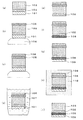
次に、第1の実施例を説明する。本発明の第1の実施例を、図1の断面構造図による製造工程図によって説明する。
【0032】
この第1実施例では、第1基板(例えばガラス基板)上に、モリブデン薄膜からなる保護層を形成した後、薄膜デバイスを形成する既知の技術を用いて、保護層上に、いわゆる低温ポリシリコン技術を使って薄膜トランジスタを備えた薄膜デバイス層を形成し、その後、弗化水素酸エッチングをすることによって、上記第1基板の除去を行った。エッチングの保護層は、スパッタリング法にてモリブデン(Mo)薄膜を例えば500nmの厚さに成膜して形成した。
【0033】
上記第1基板のエッチングまでの工程を以下に説明する。まず図1(a)に示すように、第1基板(例えば厚さ0.7mmのガラス基板)101上に、スパッタリング法にて、保護層102としてモリブデン(Mo)薄膜を例えば500nmの厚さに成膜して形成した。この保護層102のモリブデン薄膜の厚さは例えば0.1μm〜1μmの厚さの範囲で選択される。さらに、薄膜デバイスを形成する既知の技術を用いて、保護層102上に、いわゆる低温ポリシリコン技術を使って薄膜トランジスタを備えた薄膜デバイス層103を形成した。例えば液晶ディスプレー技術(松本正一 編著、産業図書発行、1996年)p.115≡118に記載されているような低温ポリシリコントップゲート型TFTプロセスで薄膜デバイス層103を形成した。なお、薄膜デバイス層103を被覆層(図示せず)により被覆してもよい。以下、被覆層を形成しない場合を説明する。
【0034】
その後、図1(b)に示すようにホットプレート104上に、第1基板101を載せ、このホットプレート104を80℃〜140℃に加熱しながら、薄膜デバイス層103上に第1接着層(例えばホットメルト系接着剤)105を、例えば厚さが1mm程度となるように塗布して形成した。この第1接着層の厚さは例えば0.1mm〜3mmの厚さの範囲で選択される。
【0035】
次に、図1(c)に示すように、上記第1接着層105上に、第2基板106を載せ、例えば5×l04 Paの圧力で加圧しながら室温まで冷却し第2の基板106を貼り付けた。上記第2基板106には、例えば厚さが1mmのモリブデン基板を用いた。または、第2基板上にホットメルト系接着剤を塗布して、その上に第1基板に形成された薄膜デバイス層側を載せてもよい。上記接着の際には、気泡が入ることがあるが、真空中で貼り合わせると、気泡は入らなかった。今回は、第1接着層105のホットメルト系接着剤には、エレクトロンワックスを用いた。
【0036】
なお、第2基板106はモリブデン以外でもフッ酸に耐性があるような金属、例えばタングステン(W)、インコネル625、ステンレスもしくはこれらの金属で被覆されたガラス基板、セラミックス基板、またはポリイミド板、2軸延伸ポリエチレンテレフタレート板、PEN板のような低線膨張係数のプラスチック板を用いてもよい。
【0037】
次に、図1(d)に示すように、第2基板106を貼り付けた第1基板101を例えば重量濃度50%〜60%のフッ酸水溶液107中に浸漬して、ガラス基板からなる第1基板101のエッチングを行った。ここで用いたフッ酸は、重量濃度50%で、エッチング時間は3.5時間とした。第1基板(ガラス基板)101を完全にエッチングした後は、図1(e)に示すように、保護層102が露出される。なお、エッチング生成物が保護層102上に残る場合には水洗により除去することができた。またフッ酸水溶液の濃度はこれより低くても良いが、必要に応じてエッチング時間と液温を調整する。また、エッチングの面内均一性を向上させるためにエッチング中に液を撹拌したり、循環したり、フッ酸水溶液濃度をー定に保つ機構が有効であった。
【0038】
次に、図1(f)に示すように、上記表出された保護層102の表面に第2接着層108として、紫外線硬化接着剤を塗布した。この紫外線硬化接着剤は、粘度の低いものをスピンコートにより塗布した。ただし、紫外線硬化接着剤の厚さの均一性が取れるならばどのような方法であってもよい。また、気泡を完全にとるためには、紫外線硬化接着剤を真空中で脱泡した後、真空中での接着が効果的であった。
【0039】
また、ここでは、アクリル系の紫外線硬化接着剤を用いたが、紫外線硬化接着剤である必要はなく、エポキシ系接着剤、ユリア系接着剤、ウレタン系接着剤、フェノール系接着剤、メラミン系接着剤、エマルジョン系接着剤、アクリル系接着剤、シアノアクリル酸エステル系接着剤、クロロプレンゴム系接着剤、ニトリルゴム系接着剤、ウレタンゴム系接着剤、シアノアクリレート系接着剤、スチレンブタジエンゴム系接着剤、天然ゴム系接着剤、アクリル系粘着材でもよい。
【0040】
次に、図1(g)に示すように、紫外線硬化接着剤からなる第2接着層108を形成した後、第3基板109に貼り付け、紫外線を照射して、第2接着層108を硬化させた。上記第3基板109には、例えば厚さが0.5mmのポリカーボネート基板を用いた。
【0041】
ここでは、第3基板109にポリカーボネートを用いたが、ポリカーボネートに限らず、例えばポリエチレンテレフタレート、ポリエチレンナフレート、ポリブチレンテレフタレート、ポリエーテルサルフォン、ポリオレフィン、ポリプロピレン、ポリブチレン、ポリアミド、ポリアミドイミド、ポリエーテルエーテルケトン、ポリエーテルイミド、ポリエーテルケトン、ポリアリレート、ポリスルホン、ポリフェニレンスルフィド、ポリフェニレンエーテル、ポリアセタール、ポリメチルペンテン、エポキシ樹脂、ジアリルフタレート樹脂、フェノール樹脂、不飽和ポリエステル樹脂、液晶プラスチック、ポリベンゾイミダゾール、熱硬化性ポリブタジエンなどからなる基板、またはこれらの材料からなるポリマーアロイ、ファイバー強化された単体材料基板、または同一材料の積層基板、またはこれらのうち少なくともーつを含む積層基板でもよく、ステンレス、アルミニウムなどの金属板、またはアルミナ(Al2 O3 )、シリカ(SiO2 )、シリコンカーバイド(SiC)、酸化マグネシウム(MgO)、酸化カルシウム(CaO)などを成分とするセラミックス板の単体材料基板、またはこれらのうち少なくとも一つを含む積層基板でも良い。ただし、紫外線を通さない基板については、第2接着層108には紫外線硬化接着剤以外の接着剤を使わなければならない。
【0042】
次に、図1(h)に示すように、紫外線硬化接着剤が充分に固まった後、冷却装置110の中に入れ、基板を約−15℃に冷却した。数十秒でホットメルト系接着剤からなる第1接着層105に細かいひびが入った。その状態で取り出し、端の方から物理的に剥離した。第1接着層105には接着強度がほとんど残っておらず、力をほとんど加えずに、第2基板106を剥離することができた。剥離後は、図1(i)に示すように、薄膜デバイス層103表面が露出される。このようにして、ポリカーボネート基板からなる第3基板109上に第2接着層108により保護層102を介して薄膜デバイス層103が形成された構成が得られた。
【0043】
なお、ホットメルト系接着剤以外の第1接着層105とモリブデン以外の第2基板106との組み合わせでは、第1接着層105と第2基板106との線膨張係数の違いが大きくなるほど冷却時にひびが入りやすくなり、剥離が容易になる。ひびが入った場合は、薬液に浸漬しても、ひびが伝わって薬液が浸透するため、短時間で剥離が可能になる。
【0044】
なお、上記第2基板106を分離した後、2―プロパノールにより、薄膜デバイス層103の表面についているホットメルト系接着剤を洗浄剥離した。
【0045】
次に、第2の実施例を説明する。図2(a)にデバイス作製後の状態を示す。第1の実施例と同様に、例えばスパッタリング法によって、ガラス基板からなる第1基板201上に、保護層202としてモリブデンエッチング保護層を形成し、さらに保護層202上に薄膜デバイス層203を形成した。薄膜デバイス層203は、第1の実施例と同様に低温ポリシリコン技術を用いて作製した。
【0046】
次に、図2(b)に示すように、薄膜デバイス層203上に、感温性のある粘着材を用いて第1接着層204を形成した。この第1接着層204は、室温(例えば25℃)以下にすると粘着性が著しく低下するもしくは粘着性がなくなるものであればどのような粘着材も使用することができる。例えば、炭素数10以上の直鎖状アルキル基を側鎖とするアクリル酸エステル、メタクリル酸エステル等を用いる。今回は、ニッタ株式会社製のインテリマーを使用した。このようにして、第1基板201上の薄膜デバイス層203と第2基板205となるモリブデン基板とを接着した。
【0047】
接着後、図2の(c)に示すように、フッ酸エッチング工程で、フッ酸が端部から入ってこないように、第1基板201から第2基板205までの端部を例えばホットメルト系接着剤でシール206を形成した。
【0048】
その後、前記第1実施例と同様に、第1基板のエッチング工程と第2接着層の塗布工程と第3基板の接着工程を行った。
【0049】
そして、第3基板を接着した後、約−15℃に冷却し、薄膜デバイス層とモリブデン基板からなる第2基板とを物理的に剥離した。ホットメルト系接着剤からなるシールはひび割れしており、また粘着材からなる第1接着層は接着力が無く、ほとんど力を加えることなく第2基板の剥離が行えた。
【0050】
次に、第3の実施例を説明する。第1の実施例との違いは、第1基板に石英基板を使い、薄膜デバイス層は、高温ポリシリコン技術を使うことによって作製した。第1の実施例と同様に、スパッタリング法によって、第1基板にフッ酸エッチング時の保護層として機能する保護層を、モリブデン層を例えば500nmの厚さに堆積して形成した。その後の工程は、第1の実施例と同様である。
【0051】
次に、第4の実施例を説明する。図3(a)に示すように、前記第3の実施例と同様に、第1基板401に石英基板を使い、薄膜デバイス層403は高温ポリシリコン技術を使うことにより作製した。前記第3の実施例との違いは、保護層402には、モリブデン薄膜ではなく、アモルファスシリコンを例えば10nmの厚さに成膜して用いた。このアモルファスシリコンの厚さは50nm以下であることが望ましい。この成膜方法としては、プラズマCVD法を用いた。このアモルファスシリコンの成膜は、膜中に水素を多く含むように、低温での成膜が望ましい。ただし、その後の工程で膜剥がれが起こらないことが必要である。今回は、150℃にて成膜を行った。また、低圧CVD法、大気圧(常圧)CVD法、電子サイクロトロン共鳴(以下ECRという、ECRはElectron Cyclotron Resonanceの略)CVD法、スパッタリング法等による成膜技術を用いて形成したアモルファスシリコンであっても問題はない。
【0052】
その後、前記第3の実施例と同様に、薄膜デバイス層403上に第1接着層404を形成して第2基板405を貼り合わせる。第1基板401である石英基板の分離は、紫外線照射によって行った。その結果、図3(b)に示すように、薄膜デバイス層403が露出される。上記条件で成膜を行ったアモルファスシリコンに石英基板の第1基板401側から紫外線を照射すると水素が発生し、アモルファスシリコンからなる保護層402を境界として薄膜デバイス層403と第1基板401との分離が起こる。
【0053】
なお、上記紫外線の照射には、エキシマレーザ(例えばXeClレーザ:波長=308nm)を用いた。ただし、100nm〜350nmの紫外線であるならば、他の波長の紫外線であってもよい。その後の工程は第3の実施例と同様である。
【0054】
次に、第5の実施例を説明する。第1の実施例との違いは、第1基板に石英基板もしくはガラス基板を支持基板とするSOI(Silicon on insulator)基板を用いた点にある。この場合はフッ酸によるエッチングにおいて、石英もしくはガラスと、シリコンとではエッチング速度が異なるため、シリコンウエハが自動的に保護層として働く。そのため、スパッタリング法によってモリブデン薄膜を形成する必要はない。薄膜デバイス層は、一般的なLSI技術を用いて形成した。その後の工程は、第1の実施例と同様である。
【0055】
上記説明した本発明の薄膜デバイスの製造方法によれば、冷却することによって第1接着層の接着強度を弱めて第2基板を分離するので、薄膜デバイスの転写技術において時間のかかる処理である接着層の剥離を短時間で、なおかつ大面積で行うことができる。そのため、転写工程のスループットを高めることができる。また、製造基板(第1基板)と実使用基板(第3基板)とを別にできるため、実使用基板の耐熱性などを考慮に入れる必要がなくなり、薄膜デバイスの軽量化、薄型化、堅牢化が可能になる。それによって、プラスチック基板のような耐熱性の低い基板上に薄膜デバイス層を搭載した薄膜デバイスを得ることができる。また、本発明の薄膜デバイスの製造方法を実現するための製造装置は、現行の生産ラインをそのまま使用することが可能であるため、新たな設備投資を必要としない。
【0056】
さらに、本発明の製造方法により得られる薄膜デバイスは、液晶表示パネルや有機エレクトロルミネッセンス表示パネルのアクティブマトリクス型駆動基板として好ましく利用することができる。例えば、アクティブマトリクス型駆動基板としての薄膜デバイスと、透光性プラスチック基板に透明導電膜を形成した対向基板とから液晶セルを構成すると非ガラス基板液晶表示パネルが得られる。この場合、アクティブマトリクス型駆動基板または対向基板のいずれかにカラーフィルター層を設ければ、非ガラス基板フルカラー液晶表示パネルとなる。また、アクティブマトリクス型駆動基板としての薄膜デバイスの上に有機エレクトロルミネッセンス層を設ければ、非ガラス基板有機エレクトロルミネッセンス表示パネルが得られる。
【0057】
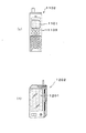
これらの表示パネルは、携帯情報端末機や携帯電話機等に好ましく組み込むことができる。例えば、図4(a)に示すように、液晶パネルからなる表示部1101を有する携帯電話機1102であって、液晶表示パネル上に保護板がフロントケース1103と一体化されて被せられ、表示部1101の最外面が構成されるようにしたものや、図4(b)に示すように、タッチパネル付きの表示部1201を有する携帯情報端末機1202であって、この携帯情報端末機1202自体の操作と、必要に応じて携帯情報端末機1202に装着される無線電話、録音再生機能、ディジタルカメラ機能等のオプション機器の制御を表示部1201のタッチパネルで操作できるようにしたものなど、種々の機器の液晶表示装置として使用される。
【0058】
なお、本発明の薄膜デバイスの製造方法によれば、以下のような効果も期待できる。
【0059】
すなわち、異なるプロセスで作製した薄膜デバイスを同一非ガラス基板上に集積することが可能になる。例えば駆動能力に優れたCMOS回路構成が可能な低温ポリシリコンTFTで、パネル周辺部分の駆動回路を作製し、低コストで大面積にわたり特性を均一にしやすいアモルファスシリコンデバイスで表示部(画素部)のスイッチング回路部を作製し、両者を同一の非ガラス基板上に集積し、デバイス間配線を別途施すことで、低温ポリシリコン≡アモルファスシリコン複合駆動基板を低温ポリシリコン単独プロセスによるよりも容易に製作することが可能となる。この場合、高コストの微細化プロセスを、低温ポリシリコンプロセスで製造される、パネル周辺部分の駆動回路部分に限定して使用することで、低コスト化も同時に達成される。
【0060】
また、薄膜デバイス層を形成する際には、石英基板、シリコン基板、ガリウム基板等の耐熱温度の高い基板を用いることができるので、プロセス温度の低下によってデバイスの性能や信頼性が低下するおそれがない。薄膜デバイス層の作製時における真空中のプロセスにおいては、プラスチック基板からの脱ガスによるデバイス汚染がない。プラスチック基板につきもののプロセスにおける温度履歴による膨張、収縮、変形の影響を受けないので、配線の断線やデバイス層のクラックの危険がない。
【0061】
さらに第3基板は薄膜デバイス層の作製時には使わないので、表面粗さに対する要求も、第1基板よりはずっと緩い。そのため、従来のガラス基板やシリコンウエハ以外にも、プラスチック基板、金属基板やセラミック基板が使用可能となり、表示パネル設計の選択肢が増えるという利点もある。
【0062】
【発明の効果】
本発明によれば、第2基板を分離する際に冷却することによって第1接着層の接着強度を弱めるので、薄膜デバイスの転写技術において時間のかかる処理である接着層の剥離を短時間で、なおかつ大面積で行うことができる。そのため、転写工程を高い生産性で行うことができる。このように実用的な速度で転写技術ができるようになると、製造基板と実使用基板とを別にできるため、耐熱性などを考慮に入れる必要がなくなり、薄膜デバイスの軽量化、薄型化、堅牢化が可能になる。また、製造装置に関しても、現行の生産ラインをそのまま使えるため、投資効率が高い。
【図面の簡単な説明】
【図1】 本発明の第1の実施例による薄膜デバイスの製造工程図である。
【図2】 本発明の第2の実施例による薄膜デバイスの製造工程図である。
【図3】 第4の実施例による薄膜デバイスの製造工程図である。
【図4】 本発明の製造方法で得られた薄膜デバイスを備えた携帯電話機(a)及び携帯情報端末機(b)の外観図である。
【符号の説明】
101…第1基板、102…保護層、103…薄膜デバイス層、105…第1接着層[0001]
BACKGROUND OF THE INVENTION
The present invention relates to a method for manufacturing a thin film device and a display device. More specifically, the present invention is used for a flat display panel using liquid crystal or electroluminescence (hereinafter abbreviated as EL), for example, a thin film transistor (Thin Film Transistor, A method for manufacturing a thin film device constituting an active matrix type drive substrate using TFT) and a non-glass substrate, that is, a plastic substrate, a ceramic substrate, a metal substrate, and a thin film device used for a display panel. The present invention relates to a display device.
[0002]
[Prior art]
In recent years, there has been an increasing demand for thinning, thinning, and weight reduction of thin film devices constituting liquid crystal display panels, EL display panels, and the like used for portable information terminals such as mobile phones and PDAs. For example, in the liquid crystal display panel, in order to meet these demands, in addition to the initial thinning of the glass substrate, there is a technique for thinning the glass substrate by mechanical polishing or chemical etching after bonding the driving substrate and the counter substrate. Some are used.
[0003]
[Problems to be solved by the invention]
However, since a thin film device is manufactured in an environment of high temperature and vacuum, there are restrictions on a substrate used for manufacturing. For example, in a liquid crystal display device using a thin film transistor, a quartz substrate that can withstand a temperature of 1000 ° C. and a glass substrate that can withstand a temperature of 500 ° C. are used. Although thinning of these substrates has been studied, as long as a quartz substrate or a glass substrate is used, the substrate size must be reduced in order to prevent a decrease in substrate rigidity, resulting in a decrease in productivity. Moreover, since the processing time of a glass thinning process increases, there exists a subject that the practical thickness of the drive substrate which comprises a display panel cannot be 0.3-0.4 mm or less. Further, when the glass plate thickness is reduced, the flexure increases in inverse proportion to the cube of the plate thickness, so that the robustness important for portable information terminal applications is drastically reduced, which becomes a limiting factor beyond productivity. As described above, the performance required for the manufacturing substrate is different from the performance required for actual use.
[0004]
For this reason, it is demanded that a thin and light plastic substrate can be used instead of a glass substrate serving as a base for a thin film transistor substrate used for a liquid crystal display panel or the like. Is expensive.
[0005]
In addition, a technique for transferring a thin film device formed on a production substrate having a high heat-resistant temperature to an actual use substrate has been studied. As the transfer process, both one-time transfer and two-time transfer have been studied, and the two-time transfer has an advantage that it is easy to apply to the current process because there is no upside down of the device layer with respect to the substrate. In the transfer transcription technique, since an adhesive is generally used as a temporary temporary fixing, a process of peeling after bonding once is essential.
[0006]
When the adhesive strength of the adhesive layer is weakened by heat, it is generally necessary to raise the temperature to about 100 ° C., but the thin film device layer is cracked due to the thermal contraction or thermal expansion behavior of the third substrate and the thin film device layer. There was a problem. Moreover, this problem can be solved if there is an adhesive whose adhesive strength is weakened at a low temperature. However, for example, paraffin (melting point: 50 ° C.) has low adhesive strength, and cracks or wrinkles occur when the first substrate is peeled off. No suitable adhesive has been found.
[0007]
Further, when the adhesive strength of the adhesive layer is weakened by immersion in the chemical solution, the adhesive between the thin film device layer and the second substrate is very narrow, and the chemical solution must penetrate between the thin film device layer and the second substrate. However, when the substrate becomes large, it takes time rapidly, and there is a problem that productivity does not increase.
[0008]
The present invention makes it possible to manufacture a thin film device suitable for a lightweight and thin display panel without impairing the robustness. Furthermore, a technique for transferring a thin film device from a production substrate to an actual use substrate in a short time is provided.
[0009]
[Means for Solving the Problems]
The present invention provides a first substrate In A protective layer having resistance to hydrofluoric acid is formed, a thin film device layer or a thin film device layer and a coating layer covering the thin film device layer are formed on the protective layer, and a first adhesion is formed on the thin film device layer or the coating layer. After bonding the second substrate through the layer, a chemical solution containing hydrofluoric acid was used. By chemical etching The first substrate is completely or partially removed, and the third substrate is bonded to the protective layer covering the first substrate side of the thin film device layer or the first substrate of the thin film device layer through the second adhesive layer, and then cooled. By , Due to the difference in coefficient of linear expansion between the second substrate and the first adhesive layer, causing peeling at the interface between the second substrate and the first adhesive layer, Provided is a method of manufacturing a thin film device including a step of debonding a second substrate by weakening the adhesive strength of a first adhesive layer.
[0010]
Thus, by cooling, Second substrate Due to the difference in linear expansion coefficient between the second substrate and the first adhesive layer, peeling occurs, descend . After reducing the adhesive strength, it peels mechanically. Alternatively, when the adhesive layer cracks when cooled, it can be peeled off in a short time by immersing in a chemical solution.
[0011]
DETAILED DESCRIPTION OF THE INVENTION
The manufacturing method of the thin film device of the present invention includes (1) a step of bonding a second substrate to a thin film device layer provided on a protective layer formed on the first substrate via the first adhesive layer, (2) Next, a chemical containing hydrofluoric acid was used. By chemical etching A step of completely or partially separating or removing the first substrate; (3) Next, the first protective substrate covered with the exposed protective layer or the partially removed first substrate through the second adhesive layer. (3) Next, by cooling the three substrates , Due to the difference in coefficient of linear expansion between the second substrate and the first adhesive layer, causing peeling at the interface between the second substrate and the first adhesive layer, Including a step of debonding the second substrate by weakening the adhesive strength of the first adhesive layer. Hereinafter, each process will be described.
[0012]
In the step (1), the second substrate is bonded to the thin film device layer provided on the protective layer formed on the first substrate via the first adhesive layer. A coating layer that covers the thin film device layer may be formed.
[0013]
Examples of the first substrate include glass, quartz, silicon, gallium arsenide, gallium phosphide, silicon carbide (SiC), and sapphire. Of these, a glass substrate with a low acquisition cost is preferable.
[0014]
A protective layer functions as a stopper layer with respect to the chemical process in the process (2) mentioned later. As such a protective layer, a layer having resistance to chemicals used for chemical treatment is used. For example, when the first substrate is glass, quartz, or silicon, chemical etching using a chemical solution containing hydrofluoric acid is preferable as the chemical treatment. Therefore, the protective layer includes molybdenum (Mo), tungsten (W). , Stainless steel, inconel, amorphous Si, amorphous Si containing hydrogen, polycrystalline silicon, etc., metal layer having resistance to hydrofluoric acid, diamond thin film having resistance to hydrofluoric acid, or diamond-like carbon Preferred is a thin film. The thickness of the protective film is usually 0.1 to 5 μm. The formation of the protective layer can be appropriately determined according to the material. For example, in the case of a molybdenum thin film, it can be formed by a sputtering method or a vacuum evaporation method.
[0015]
The thin film device layer includes at least one of a thin film transistor, a thin film diode, a capacitor or a resistor formed by a so-called low-temperature polysilicon process having a substrate temperature of 500 ° C. or less or a so-called amorphous silicon process having a substrate temperature of 400 ° C. or less. preferable.
[0016]
As the first adhesive layer, a thermoplastic adhesive (hot melt) adhesive can be used as a material whose adhesive strength is reduced at low temperatures. For example, ethylene ≡ vinyl acetate thermoplastic elastomer, styrene ≡ butadiene block copolymer, styrene ≡ ethylene ≡ butylene block copolymer, styrene ≡ isoprene block copolymer, ethylene ≡ vinyl chloride copolymer, acetate acetate resin, poly Vinyl chloride, polyethylene, polypropylene, polymethylpentene, polybutene, thermoplastic polybutadiene, polystyrene, polybutadiene, polyvinyl acetate, polymethyl methacrylate, polyvinylidene chloride, polyvinyl alcohol, polytetrafluoroethylene, ethylene≡tetrafluoroethylene copolymer, Acrylonitrile ≡ styrene copolymer (AS resin), acrylonitrile butadiene styrene (ABS resin), ionomer, AAS resin, ACS resin, polyacetal, polycar Nate, polyphenylene ether, polyethylene terephthalate, polybutylene terephthalate, polyarylate, polysulfone, polyethersulfone, polyimide, polyamide, polyamideimide, polyphenylene sulfide, polyoxybenzoyl, polyetheretherketone, polyetherimide, liquid crystal polyester, cellulosic plastic (Cellulose acetate, cellulose acetate butyrate, ethyl cellulose, celluloid cellophane), polyolefin, polyurethane, and the above copolymers and polymer alloys, and wax, coal tar, rosin, natural rubber, fluororubber, and the like.
[0017]
The thickness of the first adhesive layer is 0.1 mm to 3 mm. The first adhesive layer can be formed by a conventional method such as a coating method.
[0018]
The second substrate is preferably molybdenum (Mo), tungsten (W), stainless steel, inconel (for example, inconel 625 (composition is Ni> 58%, Cr 20% to 23%, Fe <5%, Mo8% to 10). %, Nb 3.1% to 4.2%)), etc., acid-resistant metal plates or laminates thereof, metal plates or glass plates or ceramics plates coated with these acid-resistant metal films, or laminates thereof But you can. Alternatively, a plastic plate having a low linear expansion coefficient such as polyethylene terephthalate (for example, biaxially stretched PET), polyethylene naphthalate, polyethersulfone, or polyimide may be used.
[0019]
The bonding of the second substrate can be performed according to the characteristics of the first adhesive layer to be used. For example, when the first adhesive layer is a thermoplastic adhesive (hot melt adhesive), heating with a hot plate is performed. It can be done by processing.
[0020]
When a single second substrate is bonded to the thin film device layer provided on the protective layer formed on each of the plurality of first substrates via the first adhesive layer, different thin film device layers are provided. It can be formed on one third substrate.
[0021]
Next, step (2) is performed. That is, the first substrate is completely or partially removed by a process including at least one of chemical treatment and mechanical polishing treatment.
[0022]
The chemical treatment can be determined according to the material of the first substrate. Also. As the mechanical polishing treatment, so-called chemical mechanical polishing (CMP) is preferably exemplified. Both chemical treatment and mechanical polishing treatment are preferably performed. In that case, it is preferable to perform both treatments simultaneously or to perform chemical treatment subsequent to the mechanical polishing treatment.
[0023]
The first substrate may be completely removed (that is, until the protective layer is exposed) or partially (only the first substrate that is slightly thin remains), but is completely removed until the protective layer is exposed. It is preferable to do.
[0024]
In at least one of the chemical treatment and the mechanical polishing treatment, the treatment of the thin film device layer is performed on the outer peripheral region of the adhesive body in a state where the first substrate and the second substrate are adhered to the upper and lower sides of the thin film device layer. It is preferable to provide a seal portion that prevents liquid from entering. The seal portion can be formed from a material that is resistant to chemical treatment (for example, a hot melt adhesive).
[0025]
Next, step (3) is performed. That is, the third substrate is bonded to the exposed protective layer or the protective layer covered with the partially removed first substrate through the second adhesive layer.
[0026]
As the second adhesive layer, a two-component curable adhesive or an ultraviolet curable adhesive can be preferably exemplified.
[0027]
As the third substrate, a base material having a heat resistant temperature of 100 ° C. or higher is preferable, and specifically, polycarbonate can be exemplified, but other examples include polyethylene terephthalate, polyethylene naphthalate, polybutylene terephthalate, polyethersulfone, polyolefin, polypropylene, Polybutylene, polyamide, polyamideimide, polyetheretherketone, polyetherimide, polyetherketone, polyarylate, polysulfone, polyphenylene sulfide, polyphenylene ether, polyacetal, polymethylpentene, epoxy resin, diallyl phthalate resin, phenol resin, siloxane resin Group consisting of acrylic resin, unsaturated polyester resin, liquid crystal plastic, polybenzimidazole, thermosetting polybutadiene, etc. Or a polymer alloy made of these materials, a fiber reinforced single material substrate, a laminated substrate of the same material, or a laminated substrate including at least one of them, a metal plate such as stainless steel or aluminum, or alumina ( Al 2 O Three ), Silica (SiO 2 ), A single material substrate of a ceramic plate containing silicon carbide (SiC), magnesium oxide (MgO), calcium oxide (CaO), or a laminated substrate including at least one of them. However, for a substrate that does not transmit ultraviolet light, an adhesive other than the ultraviolet curable adhesive must be used for the second
[0028]
Prior to adhesion to the third substrate, the protective layer may be removed to ensure translucency. The removal method can be appropriately determined according to the material of the protective layer.
[0029]
Next, step (4) is performed. That is, after the third substrate is attached, the second substrate is peeled off by cooling to reduce the adhesive force of the first adhesive layer. The principle that the adhesive force is reduced is that the adhesive layer itself changes, so that peeling occurs at the interface between the second substrate and the first adhesive layer due to the difference in the linear expansion coefficient between the second substrate and the case where the adhesive force is lost. In some cases, the adhesive strength is reduced. After reducing the adhesive strength, it physically peels off. If the adhesive layer cracks when cooled, it can be peeled off in a short time by immersing it in a chemical solution. Therefore, the cooling temperature is set to a temperature at which the adhesive force of the first adhesive layer is weakened to an adhesive force that can peel the second substrate. This temperature is appropriately selected depending on the adhesive used for the first adhesive layer.
[0030]
Hereinafter, the present invention will be specifically described with reference to the following examples.
[0031]
Next, a first embodiment will be described. A first embodiment of the present invention will be described with reference to a manufacturing process diagram according to the cross-sectional structure diagram of FIG.
[0032]
In this first embodiment, a so-called low-temperature polysilicon is formed on a protective layer using a known technique of forming a thin film device after forming a protective layer made of a molybdenum thin film on a first substrate (for example, a glass substrate). A thin film device layer including a thin film transistor was formed using a technique, and then the first substrate was removed by performing hydrofluoric acid etching. The protective layer for etching was formed by forming a molybdenum (Mo) thin film to a thickness of, for example, 500 nm by a sputtering method.
[0033]
The steps up to the etching of the first substrate will be described below. First, as shown in FIG. 1A, a molybdenum (Mo) thin film having a thickness of, for example, 500 nm is formed as a
[0034]
1B, the
[0035]
Next, as shown in FIG. 1C, the
[0036]
Note that the
[0037]
Next, as shown in FIG. 1D, the
[0038]
Next, as shown in FIG. 1 (f), an ultraviolet curable adhesive was applied as the second
[0039]
In addition, acrylic UV curable adhesive is used here, but it is not necessary to be UV curable adhesive. Epoxy adhesive, urea adhesive, urethane adhesive, phenol adhesive, melamine adhesive Agent, emulsion adhesive, acrylic adhesive, cyanoacrylate adhesive, chloroprene rubber adhesive, nitrile rubber adhesive, urethane rubber adhesive, cyanoacrylate adhesive, styrene butadiene rubber adhesive Natural rubber adhesives and acrylic adhesives may also be used.
[0040]
Next, as shown in FIG. 1G, after forming a second
[0041]
Here, polycarbonate is used for the
[0042]
Next, as shown in FIG. 1 (h), after the UV-curing adhesive was sufficiently hardened, it was placed in the
[0043]
In the combination of the first
[0044]
After separating the
[0045]
Next, a second embodiment will be described. FIG. 2A shows a state after device fabrication. Similarly to the first embodiment, a molybdenum etching protective layer was formed as the
[0046]
Next, as shown in FIG. 2B, a first
[0047]
After the bonding, as shown in FIG. 2 (c), in the hydrofluoric acid etching step, the end portions from the
[0048]
Thereafter, similarly to the first example, an etching process for the first substrate, a coating process for the second adhesive layer, and a bonding process for the third substrate were performed.
[0049]
And after bonding the 3rd board | substrate, it cooled to about -15 degreeC and physically peeled the thin film device layer and the 2nd board | substrate which consists of a molybdenum substrate. The seal made of the hot-melt adhesive was cracked, and the first adhesive layer made of the adhesive material had no adhesive force, and the second substrate could be peeled off with almost no force.
[0050]
Next, a third embodiment will be described. The difference from the first embodiment is that a quartz substrate is used as the first substrate, and the thin film device layer is manufactured by using high-temperature polysilicon technology. As in the first example, a protective layer functioning as a protective layer during hydrofluoric acid etching was formed on the first substrate by depositing a molybdenum layer to a thickness of 500 nm, for example, by sputtering. The subsequent steps are the same as in the first embodiment.
[0051]
Next, a fourth embodiment will be described. As shown in FIG. 3A, as in the third embodiment, a quartz substrate is used as the
[0052]
Thereafter, similarly to the third embodiment, a first
[0053]
Note that an excimer laser (for example, XeCl laser: wavelength = 308 nm) was used for the ultraviolet irradiation. However, as long as it is ultraviolet rays of 100 nm to 350 nm, ultraviolet rays of other wavelengths may be used. The subsequent steps are the same as in the third embodiment.
[0054]
Next, a fifth embodiment will be described. The difference from the first embodiment is that an SOI (Silicon on insulator) substrate using a quartz substrate or a glass substrate as a supporting substrate is used as the first substrate. In this case, in etching with hydrofluoric acid, the etching rate differs between quartz or glass and silicon, so that the silicon wafer automatically functions as a protective layer. Therefore, it is not necessary to form a molybdenum thin film by a sputtering method. The thin film device layer was formed using general LSI technology. The subsequent steps are the same as in the first embodiment.
[0055]
According to the method of manufacturing a thin film device of the present invention described above, the second substrate is separated by cooling to reduce the adhesive strength of the first adhesive layer. Therefore, the adhesion is a time-consuming process in the transfer technology of the thin film device. Layer peeling can be performed in a short time and in a large area. Therefore, the throughput of the transfer process can be increased. In addition, since the production substrate (first substrate) and the actual use substrate (third substrate) can be separated, it is not necessary to take into consideration the heat resistance of the actual use substrate, and the thin film device is lighter, thinner and more robust. Is possible. Accordingly, a thin film device in which a thin film device layer is mounted on a substrate having low heat resistance such as a plastic substrate can be obtained. Moreover, the manufacturing apparatus for realizing the method for manufacturing a thin film device of the present invention can use the current production line as it is, and therefore does not require new capital investment.
[0056]
Furthermore, the thin film device obtained by the production method of the present invention can be preferably used as an active matrix drive substrate for a liquid crystal display panel or an organic electroluminescence display panel. For example, a non-glass substrate liquid crystal display panel can be obtained by forming a liquid crystal cell from a thin film device as an active matrix driving substrate and a counter substrate in which a transparent conductive film is formed on a light-transmitting plastic substrate. In this case, if a color filter layer is provided on either the active matrix driving substrate or the counter substrate, a non-glass substrate full-color liquid crystal display panel is obtained. Further, if an organic electroluminescence layer is provided on a thin film device as an active matrix drive substrate, a non-glass substrate organic electroluminescence display panel can be obtained.
[0057]
These display panels can be preferably incorporated in a portable information terminal, a cellular phone, or the like. For example, as shown in FIG. 4A, a
[0058]
In addition, according to the manufacturing method of the thin film device of this invention, the following effects can also be expected.
[0059]
That is, thin film devices manufactured by different processes can be integrated on the same non-glass substrate. For example, a low-temperature polysilicon TFT with excellent driving capability and a low-temperature polysilicon TFT can be used to produce a driving circuit in the periphery of the panel, and an amorphous silicon device that can easily achieve uniform characteristics over a large area at a low cost. Fabricate the switching circuit part, integrate them on the same non-glass substrate, and separate the wiring between devices, making it easier to fabricate a low-temperature polysilicon ≡ amorphous silicon composite drive substrate than by low-temperature polysilicon single process It becomes possible. In this case, the cost reduction can be achieved at the same time by using a high-cost miniaturization process limited to the drive circuit portion in the peripheral portion of the panel manufactured by the low-temperature polysilicon process.
[0060]
In addition, when forming a thin film device layer, a substrate having a high heat-resistant temperature such as a quartz substrate, a silicon substrate, or a gallium substrate can be used. Absent. In the process in vacuum at the time of manufacturing the thin film device layer, there is no device contamination due to degassing from the plastic substrate. Since there is no influence of expansion, contraction, or deformation due to temperature history in the process inherent to plastic substrates, there is no danger of wire breakage or device layer cracking.
[0061]
Furthermore, since the third substrate is not used when the thin film device layer is manufactured, the requirement for the surface roughness is much looser than that of the first substrate. Therefore, in addition to the conventional glass substrate and silicon wafer, a plastic substrate, a metal substrate, and a ceramic substrate can be used, and there is an advantage that choices of display panel design increase.
[0062]
【The invention's effect】
According to the present invention, since the adhesive strength of the first adhesive layer is weakened by cooling when separating the second substrate, the peeling of the adhesive layer, which is a time-consuming process in the transfer technology of the thin film device, is performed in a short time. Moreover, it can be performed in a large area. Therefore, the transfer process can be performed with high productivity. When transfer technology can be performed at a practical speed in this way, manufacturing substrates and actual substrates can be separated, eliminating the need to consider heat resistance, etc., making thin-film devices lighter, thinner, and more robust Is possible. Also, with regard to manufacturing equipment, investment efficiency is high because the current production line can be used as it is.
[Brief description of the drawings]
FIG. 1 is a manufacturing process diagram of a thin film device according to a first embodiment of the invention.
FIG. 2 is a manufacturing process diagram of a thin film device according to a second embodiment of the present invention.
[Fig. 3] 4th It is a manufacturing-process figure of the thin film device by the Example of.
FIG. 4 is an external view of a cellular phone (a) and a portable information terminal (b) provided with a thin film device obtained by the manufacturing method of the present invention.
[Explanation of symbols]
DESCRIPTION OF
Claims (4)
弗化水素酸を含む薬液を用いた化学エッチングにより前記第1基板を完全または部分的に分離または除去する工程と、
前記薄膜デバイス層の第1基板側もしくは前記薄膜デバイス層の第1基板を被覆する保護層に、第2接着層を介して第3基板を接着する工程と、
冷却することによって、前記第2基板と前記第1接着層との線膨張係数の違いにより前記第2基板と前記第1接着層との界面で剥離を起こして、前記第1接着層の接着強度を弱めて前記第2基板を剥離する工程とを有する
薄膜デバイスの製造方法。A protective layer having hydrofluoric acid resistance is formed on the first substrate, and a thin film device layer or a thin film device layer and a covering layer covering the thin film device layer are formed on the protective layer, and the thin film device layer or the covering layer is formed on the thin film device layer or the covering layer. Bonding the second substrate via the first adhesive layer;
Separating or removing the first substrate completely or partially by chemical etching using a chemical solution containing hydrofluoric acid;
Adhering a third substrate through a second adhesive layer to the first substrate side of the thin film device layer or a protective layer covering the first substrate of the thin film device layer;
By cooling, peeling occurs at the interface between the second substrate and the first adhesive layer due to a difference in linear expansion coefficient between the second substrate and the first adhesive layer, and the adhesive strength of the first adhesive layer And a step of peeling off the second substrate by weakening the thickness of the thin film device.
請求項1記載の薄膜デバイスの製造方法。The method for manufacturing a thin film device according to claim 1, wherein after the adhesive strength of the first adhesive layer is weakened, the second substrate is mechanically peeled off.
薄膜デバイス。The protective layer is formed having a hydrofluoric acid resistance to the first substrate, the thin film device layer on the protective layer, or forming a thin film device layer and the coating layer covering this, the thin film device layer or coating layer The thin film device layer is bonded to the second substrate through the first adhesive layer and then completely or partially separated or removed by chemical etching using a chemical solution containing hydrofluoric acid. By adhering the third substrate to the protective layer covering the first substrate side of the thin film device layer or the first substrate of the thin film device layer via the second adhesive layer and further cooling , the second substrate and the first adhesive It is formed by peeling at the interface between the second substrate and the first adhesive layer due to the difference in linear expansion coefficient from the layer, and peeling off the second substrate by weakening the adhesive strength of the first adhesive layer. Thin film device.
表示装置。The protective layer is formed having a hydrofluoric acid resistance to the first substrate, the thin film device layer on the protective layer, or forming a thin film device layer and the coating layer covering this, the thin film device layer or coating layer The thin film device layer is bonded to the second substrate through the first adhesive layer and then completely or partially separated or removed by chemical etching using a chemical solution containing hydrofluoric acid. By adhering the third substrate to the protective layer covering the first substrate side of the thin film device layer or the first substrate of the thin film device layer via the second adhesive layer and further cooling , the second substrate and the first adhesive It is formed by peeling at the interface between the second substrate and the first adhesive layer due to the difference in linear expansion coefficient from the layer, and peeling off the second substrate by weakening the adhesive strength of the first adhesive layer. Display device that uses thin film devices.
Priority Applications (1)
| Application Number | Priority Date | Filing Date | Title |
|---|---|---|---|
| JP2002118937A JP4186502B2 (en) | 2002-04-22 | 2002-04-22 | Thin film device manufacturing method, thin film device, and display device |
Applications Claiming Priority (1)
| Application Number | Priority Date | Filing Date | Title |
|---|---|---|---|
| JP2002118937A JP4186502B2 (en) | 2002-04-22 | 2002-04-22 | Thin film device manufacturing method, thin film device, and display device |
Publications (2)
| Publication Number | Publication Date |
|---|---|
| JP2003316281A JP2003316281A (en) | 2003-11-07 |
| JP4186502B2 true JP4186502B2 (en) | 2008-11-26 |
Family
ID=29535638
Family Applications (1)
| Application Number | Title | Priority Date | Filing Date |
|---|---|---|---|
| JP2002118937A Expired - Fee Related JP4186502B2 (en) | 2002-04-22 | 2002-04-22 | Thin film device manufacturing method, thin film device, and display device |
Country Status (1)
| Country | Link |
|---|---|
| JP (1) | JP4186502B2 (en) |
Families Citing this family (7)
| Publication number | Priority date | Publication date | Assignee | Title |
|---|---|---|---|---|
| JP4102788B2 (en) | 2004-08-16 | 2008-06-18 | シャープ株式会社 | Manufacturing method of liquid crystal display device |
| KR101285442B1 (en) | 2005-08-09 | 2013-07-12 | 아사히 가라스 가부시키가이샤 | Thin sheet glass laminate and method for manufacturing display using thin sheet glass laminate |
| JP4738097B2 (en) * | 2005-08-19 | 2011-08-03 | 東芝モバイルディスプレイ株式会社 | Liquid crystal display device and manufacturing method thereof |
| JP2008013389A (en) | 2006-07-04 | 2008-01-24 | Nec Corp | Etching device and method for manufacturing thin type glass substrate |
| JP4648422B2 (en) * | 2008-04-25 | 2011-03-09 | 東芝モバイルディスプレイ株式会社 | Manufacturing method of display element |
| JP5547901B2 (en) * | 2009-03-25 | 2014-07-16 | 株式会社ジャパンディスプレイ | Display device |
| CN105593971B (en) * | 2013-09-25 | 2018-10-02 | 芝浦机械电子株式会社 | The removing method of substrate board treatment, the stripping means of adhesive substrates and bonding agent |
Family Cites Families (6)
| Publication number | Priority date | Publication date | Assignee | Title |
|---|---|---|---|---|
| JPH1126733A (en) * | 1997-07-03 | 1999-01-29 | Seiko Epson Corp | Transfer method of thin film device, thin film device, thin film integrated circuit device, active matrix substrate, liquid crystal display and electronic equipment |
| JP3406207B2 (en) * | 1997-11-12 | 2003-05-12 | シャープ株式会社 | Method of forming transistor array panel for display |
| JP2001102523A (en) * | 1999-09-28 | 2001-04-13 | Sony Corp | Thin-film device and manufacturing method therefor |
| JP3911929B2 (en) * | 1999-10-25 | 2007-05-09 | セイコーエプソン株式会社 | Manufacturing method of liquid crystal display device |
| JP2002023127A (en) * | 2000-07-05 | 2002-01-23 | Seiko Epson Corp | Foreign matter removing device for liquid crystal device and its method |
| JP2002100595A (en) * | 2000-07-21 | 2002-04-05 | Enya Systems Ltd | Device and method for releasing wafer and wafer treatment device using the same |
-
2002
- 2002-04-22 JP JP2002118937A patent/JP4186502B2/en not_active Expired - Fee Related
Also Published As
| Publication number | Publication date |
|---|---|
| JP2003316281A (en) | 2003-11-07 |
Similar Documents
| Publication | Publication Date | Title |
|---|---|---|
| TWI362547B (en) | Peeling method and method for manufacturing display device using the peeling method | |
| US7262088B2 (en) | Thin film device supply body, method of fabricating thin film device, method of transfer, method of fabricating semiconductor device, and electronic equipment | |
| KR101538835B1 (en) | Method for manufacturing laminate, and laminate | |
| TW574753B (en) | Manufacturing method of thin film apparatus and semiconductor device | |
| CN100392797C (en) | Stripping method | |
| JP4478268B2 (en) | Thin film device manufacturing method | |
| JP3974749B2 (en) | Functional element transfer method | |
| TWI480165B (en) | Manufacture of electronic devices | |
| KR20030089639A (en) | Active matrix type display device and method of manufacturing the same | |
| WO2007129554A1 (en) | Thin-sheet glass laminate, process for manufacturing display apparatus using the laminate, and supporting glass substrate | |
| JP2003345267A (en) | Display device and its manufacturing method | |
| WO2012060199A1 (en) | Laminate body, panel for use in display device with support board, panel for use in display device, and display device | |
| KR101026040B1 (en) | Fabrication method of thin film device | |
| JP2003066858A (en) | Method of manufacturing thin-film device substrate | |
| JP4186502B2 (en) | Thin film device manufacturing method, thin film device, and display device | |
| JP2003323132A (en) | Method for manufacturing thin film device and semiconductor device | |
| TWI222545B (en) | Method of transferring a thin film device onto a plastic sheet and method of forming a flexible liquid crystal display | |
| JP2005057227A (en) | Element resticking method | |
| JP2003068995A (en) | Method for manufacturing thin film device substrate | |
| JP2009537076A (en) | Method for forming a semiconductor-on-insulator structure | |
| JP2009231533A (en) | Peeling method, peeling apparatus and method of manufacturing semiconductor device | |
| US20210143234A1 (en) | Flexible substrate, manufacturing method thereof, and display panel having the same | |
| JP4759917B2 (en) | Thin film device manufacturing method, thin film device, and liquid crystal display device | |
| JP5103607B2 (en) | Release layer removal method | |
| WO2020008882A1 (en) | Device-layer-transferred substrate production method and device layer-transferred substrate |
Legal Events
| Date | Code | Title | Description |
|---|---|---|---|
| A621 | Written request for application examination |
Free format text: JAPANESE INTERMEDIATE CODE: A621 Effective date: 20050309 |
|
| A977 | Report on retrieval |
Free format text: JAPANESE INTERMEDIATE CODE: A971007 Effective date: 20070403 |
|
| A131 | Notification of reasons for refusal |
Free format text: JAPANESE INTERMEDIATE CODE: A131 Effective date: 20080212 |
|
| A521 | Written amendment |
Free format text: JAPANESE INTERMEDIATE CODE: A523 Effective date: 20080414 |
|
| A131 | Notification of reasons for refusal |
Free format text: JAPANESE INTERMEDIATE CODE: A131 Effective date: 20080527 |
|
| A521 | Written amendment |
Free format text: JAPANESE INTERMEDIATE CODE: A523 Effective date: 20080725 |
|
| TRDD | Decision of grant or rejection written | ||
| A01 | Written decision to grant a patent or to grant a registration (utility model) |
Free format text: JAPANESE INTERMEDIATE CODE: A01 Effective date: 20080819 |
|
| A01 | Written decision to grant a patent or to grant a registration (utility model) |
Free format text: JAPANESE INTERMEDIATE CODE: A01 |
|
| A61 | First payment of annual fees (during grant procedure) |
Free format text: JAPANESE INTERMEDIATE CODE: A61 Effective date: 20080901 |
|
| FPAY | Renewal fee payment (event date is renewal date of database) |
Free format text: PAYMENT UNTIL: 20110919 Year of fee payment: 3 |
|
| LAPS | Cancellation because of no payment of annual fees |