JP4174288B2 - Two-dimensional scanning device and scanning image display device - Google Patents
Two-dimensional scanning device and scanning image display device Download PDFInfo
- Publication number
- JP4174288B2 JP4174288B2 JP2002302385A JP2002302385A JP4174288B2 JP 4174288 B2 JP4174288 B2 JP 4174288B2 JP 2002302385 A JP2002302385 A JP 2002302385A JP 2002302385 A JP2002302385 A JP 2002302385A JP 4174288 B2 JP4174288 B2 JP 4174288B2
- Authority
- JP
- Japan
- Prior art keywords
- scanning
- lens
- dimensional
- deflection
- light beam
- Prior art date
- Legal status (The legal status is an assumption and is not a legal conclusion. Google has not performed a legal analysis and makes no representation as to the accuracy of the status listed.)
- Expired - Fee Related
Links
Images


Description
【0001】
【発明の属する技術分野】
本発明は、光を2次元方向に走査することによって2次元画像を表示する走査型画像表示装置に用いられる2次元走査装置に関するものである。
【0002】
【従来の技術】
光スポットを2次元方向に走査し、その残像効果によって2次元画像を形成する2次元走査装置は種々提案されている。
【0003】
ところで、光束が2次元的に偏向および走査されることにより、被走査面上の2次元画像に歪み、所謂ディストーションが生ずることが一般に知られている。ディストーションには、台形歪み、等速走査性のディストーション、直進走査性のディストーション、さらには被走査面上に描かれた画像の枠が湾曲することを称したTVディストーションとがある。
【0004】
特許文献1では、光源から出射した光束を偏向手段によって2次元方向に偏向し、歪曲特性としてf・sinθ特性を有した走査レンズを通して光スポットを2次元方向に走査して画像を形成する2次元走査装置が提案されている。
【0005】
これは、光の2次元方向走査によって画像を形成する際に生じる画像の歪みであるTVディストーションを、走査レンズのf・sinθ特性と電気的な補正とによって補正することができるとしたものである。
【0006】
また、特許文献2,3では、屈折面と反射面とを含む光学素子を用い、該光学素子の内部で光路を折り返すようにした2次元走査装置であって、偏心収差を補正するために屈折面もしくは反射面を面内面外ともに回転対称軸を有さない回転非対称面にて構成したものが提案されている。
【0007】
これは、1つの光学素子を用いて構成された2次元走査装置でありながらも、広い走査角にわたって、被走査面における走査光の等速性を良好に補正するものである。また、高精度な描画に必要なテレセントリック性を達成することもできるものである。
【0008】
【特許文献1】
特開平8−146320号公報
【特許文献2】
特開平11−84291号公報
【特許文献3】
特開2000−281583号公報
【0009】
【発明が解決しようとする課題】
しかしながら、特許文献1にて提案の2次元走査装置では、走査レンズのf・sinθ特性と電気的な補正とによりTVディストーションを補正しようとするものであるが、実際に電気的にTVディストーションを補正することは困難である。
【0010】
また、特許文献2,3にて提案の2次元走査装置は、そもそもTVディストーションを補正するものではない。また、2次元走査装置を構成する光学素子に光学パワーを有する反射面が設けられており、面精度が非常に厳しいことからTVディストーションを安定的に補正することが難しい。また、光学素子の内部に折り返し光路を確保する必要があるため、光学素子の厚みが増大する傾向がある。さらに、光学素子をプラスチックで構成した場合には、内部屈折率の分布や複屈折の影響を大きく受けることとなる。
【0011】
そこで、本発明は、容易かつ良好にTVディストーションや台形歪みを含むディストーションを補正することができる2次元走査装置を提供することを目的とする。
【0012】
【課題を解決するための手段】
上記の目的を達成するために、本発明の2次元走査装置は、光源からの光束を2次元方向に偏向する偏向手段と、偏向手段により偏向された光束を被走査面に向け、1枚又は2枚のレンズからなる走査光学系とを有し、光源からの光束が、偏向手段における2つの直交する偏向軸のうち少なくとも一方に対して斜め方向から入射し、走査光学系の1枚のレンズ、または2枚以内のレンズのうち被走査面に近い側のレンズは、偏向手段を反射した直後の光束の2次元偏向範囲の中心軸に対して2次元偏向範囲の最大画角よりも大きな角度をなすようにチルトした入射面と、上記中心軸に対して入射面よりも大きな角度をなすようにチルトした出射面とを有し、かつ入射面及び出射面の、それぞれの面の中心である面頂点における法線を1枚のレンズまたは被走査面に近い側のレンズの出射側に延ばしたときに、上記中心軸に対して上記法線が延びる側にシフトしており、被走査面は入射面及び出射面がチルトしている方向と同一方向にチルトしていることを特徴とする。
【0014】
また、上記入射面及び出射面のチルトした方向が、上記2つの直交する偏向軸のうちの一方の方向と同一となるようにしてもよい。
【0019】
また、上記入射面及び出射面の面頂点が、上記2次元偏向範囲外に位置し、偏向手段により偏向された光束を被走査面に導光するために該入射面及び出射面の座標中心(面頂点)から片側の部分のみが使用されるようにしてもよい。
【0024】
また、上記入射面及び出射面がアナモルフィック面であるようにしてもよい。
【0025】
また、上記入射面及び出射面が回転非対称面であるようにしてもよい。
【0026】
また、上記レンズが偏向手段側に凹面を向けたメニスカスレンズであるようにしてもよい。
【0032】
また、上記2つの直交する偏向軸のそれぞれの方向での画角が異なるようにしてもよい。
【0034】
また、偏向手段に入射する光束が収束光束であるようにしてもよい。
【0035】
さらに、被走査面におけるディストーションを、上記走査光学系により光学的に補正されるか、又は上記走査光学系による光学的補正と偏向手段を制御する回路による電気的補正との組み合わせにより補正されるようにしてもよい。
【0036】
そして、以上の2次元走査装置を用いて、プロジェクタや、ビデオカメラ、デジタルスチルカメラ等に設けられる電子ファインダといった走査型画像表示装置を構成することができる。
【0037】
この場合、光源から互いに異なる波長の複数の光束を偏向手段に入射させることによって被走査面にカラー画像を形成するようにしてもよい。
【0038】
【発明の実施の形態】
(実施形態1)
図1には、本発明の実施形態1である2次元走査装置の全体構成を示している。図2は、上記2次元走査装置の拡大図である。本実施形態および後述する各実施形態は、同装置をプロジェクタ等の画像表示装置に使用した場合の例である。
【0039】
これらの図において、1はレーザーダイオード、LED、ランプ等からなり、後述するパーソナルコンピュータ、ビデオ、DVDプレーヤー等の画像情報供給装置から入力された画像信号に応じて動作する、不図示の駆動回路によって発光制御される光源である。光源1から発せられた発散光束は、2枚の集光レンズ2a,2bを貼り合わせた集光レンズ2によって収束光束に変換され、開口絞り3によって光束幅を制限される。
【0040】
4は偏光ユニットであり、本実施形態では、1次元方向に揺動可能な反射面を有する2つの偏向器(第1偏向器4aおよび第2偏向器4b)を備えている。これら偏向器4a,4bの2つの反射面は互いに直交する2つの軸回りで揺動が可能である。また、偏向器4a,4bは、例えば、MEMS(Micro-Electro-Mechanical Systems)デバイスを用いて構成されている。MEMSデバイスを用いた偏向器4a,4bは、後述するように、その共振運動により反射面を揺動させることができる。また、MEMSデバイスは、例えば半導体製造技術などを用いたMEMS技術で作製されており、非常に小型・軽量化できる利点がある。
【0041】
光源1から発せられた光束は、第1偏向器4aによって水平方向に偏向され、この第1偏向器4aで偏向された光束は、第2偏向器4bによって垂直方向に偏向される。これにより、光源1から発せられた光束は、偏向ユニット4により2次元方向に偏向される。
【0042】
5はfθ特性を有する走査光学系である。走査光学系5は、2枚の非球面レンズ5a,5bを有しており、偏向ユニット4によって2次元方向に偏向された光束(偏向光束)を被走査面6に導くとともに、被走査面6にスポットとして結像させる。この結像スポットが第1偏向器4aによって水平方向に、第2偏向器4bによって垂直方向に走査されることにより、被走査面6に光の残像効果を利用した2次元画像が形成される。
【0043】
ここで、図3(A)には、MEMSデバイスとしての第1偏向器4aの概略構成を示している。図3(A)において、反射面4cはトーションバー4dによって筐体4eに支持されており、反射面4cの裏面に備えられた磁石が図示しないコイルから発生する磁力に反応して、トーションバー4d(偏向軸)を中心にして、1次元方向に共振振動(揺動)する。この振動する反射面4cに入射し反射した光束が水平方向(X方向)に偏向されるように、第1偏向器4aの向きが設定されている。
【0044】
図3(B)には、MEMSデバイスとしての第2偏向器4bの概略構成を示している。図3(B)において、反射面4c’はトーションバー4d’によって筐体4e’に支持されており、反射面4c’の裏面に備えられた磁石が図示しないコイルから発生する磁力に反応して、トーションバー4d’(偏向軸)を中心にして、1次元方向に共振振動(揺動)する。この振動する反射面4c’に入射し反射した光束が垂直方向(Y方向)に偏向されるように、第2偏向器4bの向きが設定されている。
【0045】
これら第1偏光器4aおよび第2偏向器4bによって、光源1からの光束を2つの偏向軸を中心(要)として2次元方向に偏向可能な偏向ユニット4が構成されている。なお、本実施形態においては、第1偏向器4aと第2偏向器4bとの間隔を3.0(mm)に設定している。
【0046】
図4には、本実施形態との比較に用いる比較例1としての2次元走査装置の水平断面(XZ断面)を示している。
【0047】
比較例1は、本実施形態と同様に、光源1から発せられた発散光束を集光レンズ2により収束光束に変換し、開口絞り3によって光束幅を制限して、偏向ユニット4によって水平および垂直方向の2次元方向に偏向される。また、比較例1には、fθ特性を有する走査光学系5’が設けられている。走査光学系5’は2枚のプラスチック製の回転対称軸を有さない回転非対称非球面レンズ5a’,5b’を有しており、偏向ユニット4によって偏向された光束(偏向光束)を被走査面6上にスポットとして結像させる。このとき、偏向ユニット4が水平および垂直方向に偏向されることにより、偏向光束は、走査光学系5’を介して被走査面6上で走査される。
【0048】
ここで、偏向ユニット4によって光束が2次元方向に偏向される範囲を2次元偏向範囲と呼び、この2次元偏向範囲における水平方向および垂直方向の中心に位置する軸(中心軸)を、本実施形態では偏向走査軸Ldcと呼ぶこととする。なお、図5には、比較例1における2次元走査装置の数値例(レンズデータ)を示している。
【0049】
図4に示した比較例1では、偏向走査軸Ldcと走査光学系5’の光軸とが一致している。走査光学系5’を構成する2枚の走査レンズ(第1走査レンズ5aおよび第2走査レンズ5b)には、偏向走査軸Ldcに対してチルトやシフトを与えておらず、全ての面の面頂点が光軸(偏向走査軸Ldc)上に配置されている。また、被走査面6にもチルトを与えておらず、走査光学系5’の光軸を通過してきた偏向光束は、被走査面6に垂直に入射する。
【0050】
このとき、被走査面6上に描かれる画像には、偏向ユニット4によって2次元方向に偏向されることに起因するTVディストーションが発生する。
【0051】
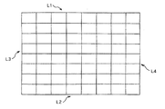
図6(A)および図6(B)を用いて、TVディストーションならびに台形歪みの算出方法を説明する。
【0052】
図6(A)は、TVディストーションの算出方法を説明する図である。TVディストーションは、表示された画像(画面)の枠が湾曲した量を示した収差量であり、図中に一点鎖線で示す画像中央を通る軸(水平軸、垂直軸)に沿った変位量を画像の幅(水平方向幅A、垂直方向幅B)で割ったものである。よって、画像枠の各辺におけるTVディストーションは以下の式で表される。
【0053】
上辺L1; a/B×100(%)
下辺L2; b/B×100(%)
左辺L3; c/A×100(%)
右辺L4; d/A×100(%)
また、図6(B)は、台形歪みの算出方法を説明する図である。台形歪みは、表示された画像の枠が傾斜した量を示した収差量であり、画像の角の変位量を画像の幅で割ったものである。よって、画像枠の各辺における台形歪みは以下の式で表される。
【0054】
上辺L1; e/2/B×100(%)
下辺L2; f/2/B×100(%)
左辺L3; g/2/A×100(%)
右辺L4; h/2/A×100(%)
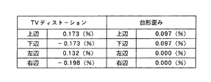
図7には、比較例1の2次元走査装置により走査表示される画像(格子)を示している。また、図8には、該表示画像におけるTVディストーションおよび台形歪みの量を示している。
【0055】
図7に示すように、画像の枠を構成する4本の線(辺)は理想的にはすべて直線になるべきであるが、枠の上辺L1および下辺L2はほぼ直線となっているものの、左辺L3および右辺L4の中央部が画像中央側に窪んだ曲線となっており、TVディストーションが大きく発生していることが分かる。このとき、TVディストーションは、上辺が0.12(%)、下辺が0.12(%)、左辺が1.53(%)、右辺が1.53(%)であった(図8参照)。比較例1では、偏向走査軸Ldcに対して走査光学系5’を対称に配置しているため、台形歪みは発生しない。
【0056】
このように、偏向走査軸Ldcに対して走査光学系5’の光軸を重ねた一般的な光学配置では、2次元方向に偏向走査することによるTVディストーションが大きく発生してしまう。そして、TVディストーションの発生により画像が歪み、表示画像の品位が劣化する。
【0057】
図9には、比較例2における2次元走査装置の水平断面(XZ断面)を示している。比較例2では、走査光学系5”は、2枚の走査レンズ(第1走査レンズ5a”および第2走査レンズ5b”)により構成されており、各走査レンズ5a”,5b”は走査光学系5”の光軸上に配置されている。走査光学系5”は水平断面内において偏向走査軸Ldcに対して偏心して配置されている。
【0058】
具体的には、水平断面内の端にて最大画角(偏向走査軸Ldcに対する最も大きな偏向角度)をなす偏向光束Bdmが走査光学系5”の光軸を通過するように偏向ユニット4の向きと位置が設定されており、最大画角と各走査レンズ5a”,5b”のチルト量とを一致させている。
【0059】
このように、各走査レンズ5a”,5b”の光軸上を水平断面内の端にある偏向光束が通過していくので、水平断面内においては、走査レンズ5a”,5b”における光軸から片側の部分のみを使用することとなり、走査レンズ5a”,5b”は光軸に対して非対称な使われ方をする。
【0060】
図10には、比較例2の2次元走査装置により走査表示される画像(格子)を示している。また、図11には、該表示画像におけるTVディストーションおよび台形歪みの量を示している。
【0061】
比較例2においては、図10に示すように、TVディストーションが左右方向(水平方向)で非対称に発生している。すなわち、偏向光束が走査レンズ5a”,5b”の光軸付近を通過する左辺側では、TVディストーションの発生量が少なく、走査レンズ5a”,5b”の光軸から離れた位置を通過する右辺側では、TVディストーションの発生量が大きくなっている。
【0062】
図11に示すように、TVディストーションは、上辺が0.90(%)、下辺が0.90(%)、左辺が0.00(%)、右辺が1.70(%)であった(図11参照)。また、台形歪みは、上辺が1.02(%)、下辺が1.02(%)、左辺が0.00(%)、右辺が0.00(%)であった(図11参照)。
【0063】
この比較例2においても、TVディストーションや台形歪みが大きく発生してしまい、表示画像の品位を劣化させる。
【0064】
そこで、本実施形態では、走査光学系5および被走査面6の配置を工夫してTVディストーションおよび台形歪みを補正している。
【0065】
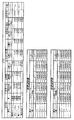
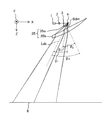
図12には、本発明の実施形態1における2次元走査装置の水平断面(XZ断面:以下の実施形態でも同様)を示している。また、図13には、上記2次元走査装置の一部を拡大して示している。また、図14には、本実施形態の2次元走査装置の数値実施例(レンズデータ)を示している。図14において、光学面の面頂点の位置を表す座標は、図13において、最大画角をなす偏向光束Bdmが第2偏向器4bで反射偏向される点を原点とし、最大画角をなす偏向光束Bdmが進む方向をZ軸とし、Z軸に対して垂直な水平方向をX軸(図13中の右方である偏向走査軸Ldcから遠ざかる方向が正)とし、Z軸とX軸に対して垂直な方向をY軸として示している。また、面間隔は、各面頂点の座標位置をZ軸方向に沿った距離で示している。
【0066】
以下、これらの図を用いて、本実施形態における走査光学系5および被走査面6の配置を説明する。
【0067】
本実施形態の走査光学系5は、2枚の走査レンズで構成され、偏向ユニット4側から第1走査レンズ5a、第2走査レンズ5bとする。
【0068】
本実施形態では、水平方向の最大画角αは偏向走査軸Ldcを中心として±20.3(deg)であり、垂直方向の最大画角は偏向走査軸Ldcを中心として±15.2(deg)である。
【0069】
まず、走査光学系5は、その光軸上を水平方向(X方向)において最大画角αをなす偏向光束Bdmの中心光線LBdmが通るように、偏向走査軸Ldcに対して偏心して配置されている。
【0070】
偏向ユニット4側に配置された第1走査レンズ5aは、その入射面および出射面の面頂点が走査光学系5の光軸(偏向光束Bdmの中心光線LBdm)上に位置するように配置されている。
【0071】
一方、被走査面6側に配置された第2走査レンズ5bは、水平方向において、走査光学系5の光軸に対してチルトおよびシフトが与えられて配置されている。本実施形態では、第2走査レンズ5bは、第2走査レンズ5bの光軸L5b(入射面の面頂点Asiでの法線および出射面の面頂点Aseでの法線:面法線)と偏向光束Bdm(中心光線LBdm)とのなす角度β’が15.6(deg) となるようにチルトしている。これにより、第2走査レンズ5bは、その光軸L5bが偏向走査軸Ldcに対して角度β=35.9(deg) をなすようにチルトしていることになる。この角度βは、最大画角α=20.3(deg) よりも15.6(deg) 大きな角度である。
【0072】
また、第2走査レンズ5bは、最大画角αをなす偏向光束Bdm上に配置されており、第2走査レンズ5bの光軸L5b(入射面の面法線)を出射側に延ばしたときに偏向走査軸Ldcに対して該光軸L5bが傾いて延びる側、つまり図12および図13中右側へ、その入射面の面頂点Asi(つまりは光軸L5b)が偏向走査軸Ldcに対して10.5(mm)離れるようにシフトしている。
【0073】
よって、第2走査レンズ5bの入射面の面頂点が最大画角の偏向光束上に配置され、第2走査レンズ5bの出射面の面頂点が偏向光束の偏向範囲(2次元偏向範囲)の外側に位置するように配置されており、第2走査レンズ5bの入出射面はそれぞれの面頂点から片側の部分のみが使用される。
【0074】
さらに、本実施形態では、水平断面内において、被走査面6(の法線)は最大画角αをなす偏向光束Bdmに対して、図12中の反時計回り方向にγ’=10.1(deg)チルトしており、偏向走査軸Ldcに対してはγ=30.4(deg)チルトしている。このとき、被走査面6は偏向走査軸Ldcに対して第2走査レンズ5bと同一方向にチルトしている。また、被走査面6も最大画角αよりも大きな角度チルトしている。
【0075】
以上のように構成される走査光学系5の2枚の走査レンズ5a,5bは、ともに回転対称軸を有さない回転非対称非球面であり、第1走査レンズ5aは負の光学パワー(焦点距離の逆数:屈折力)を有し、偏向ユニット4側に凹面を向けたメニスカスレンズである。また、第2走査レンズ5bは、偏向ユニット4側に凹面を向けたメニスカスレンズである。
【0076】
本実施形態における回転非対称非球面は、偏向光束Bdmが進む方向(Z方向)における変位量Zが、水平方向(X方向)および垂直方向(Y方向)の各位置において、次式で表現される形状となっている。
【0077】
【式1】

ここで、z;Z軸に平行な面のサグ
c;頂点の曲率
k;コーニック係数
Cj ;xmynの係数
である。
【0079】
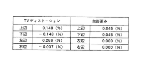
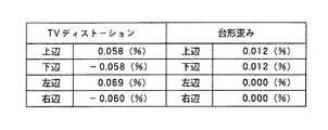
図15には、本実施形態の2次元走査装置により走査表示される画像(格子)を示している。また、図16には、該表示画像のTVディストーションおよび台形歪みの量を示している。
【0080】
図15に示した画像のTVディストーションは、枠の上辺L1が0.15(%)、下辺L2が0.15(%)、左辺L3が0.27(%)、右辺L4が0.04(%)であり、比較例で湾曲していた上辺L1および下辺L2をほぼ直線に補正している。また、台形歪みは、上辺L1および下辺L2がともに0.05(%)であり、左辺L3および右辺L4がともに0(%)であって、比較例で傾斜していた線を垂直な線に補正している。
【0081】
このように、本実施形態によれば、走査光学系5の光軸を偏向走査軸Ldcから偏心させ、走査光学系を構成する光学素子としての走査レンズ5a,5bに適切なチルトやシフトを与え、且つ被走査面6をチルトさせることにより、表示画像のTVディストーションおよび台形歪みを良好に補正することができる。
【0082】
具体的には、走査光学系5に含まれる光学素子のうち少なくとも1つの光学素子(第2走査レンズ5b)を偏向走査軸Ldcに対して最大画角αよりも大きな角度βでチルトさせ、該光学素子の入射面の面頂点での法線を出射側に延ばしたときに、偏向走査軸Ldcに対して該面法線が延びる側へシフトさせている。さらに、偏向走査軸Ldcに対して被走査面6を該光学素子と同一方向にチルトさせている。
【0083】
ここで、TVディストーションの補正メカニズムについて説明する。走査光学系(走査レンズ5a,5b)を偏向走査軸Ldcから偏心させることにより、表示画像のTVディストーションは非対称に発生する。走査光学系5の光軸付近ではTVディストーションは小さく、走査光学系5の光軸から離れるにしたがってTVディストーションは大きくなる。このとき、第2走査レンズ5bをチルトさせることにより、走査光学系5の光軸付近には殆ど影響を与えずに、走査光学系5の光軸から離れた位置のTVディストーションを補正することができる。
【0084】
つまり、走査光学系5を偏向走査軸Ldcから偏心させて配置したことと走査光学系5を構成する光学素子(第2走査レンズ5b)を走査光学系5の光軸に対してチルトさせることにより、TVディストーションを良好に補正(若しくは問題ない程度に小さく)することができる。
【0085】
これを言い換えると、走査光学系5を偏向走査軸Ldcからシフトさせることにより、TVディストーションを非対称に発生させ、走査光学系5を構成する光学素子(第2走査レンズ5b)をチルトさせることにより非対称なTVディストーションを補正することができる。このとき、いずれの偏向光束が偏向走査軸Ldcに対してなる角度よりも大きな角度(最大画角αより大きな角度)で光学素子(第2走査レンズ5b)をチルトさせることにより、TVディストーションの補正効果が大きくなる。
【0086】
次に、台形歪みの補正メカニズムを説明する。走査光学系5(走査レンズ5a,5b)を偏向走査軸Ldcから偏心させたことにより、台形歪みが発生するが、被走査面6をチルトさせることにより、逆向きの台形歪みを発生させることができる。これによって両者をキャンセルさせて台形歪みを補正することができる。
【0087】
以上により、本実施形態によれば、被走査面6に形成される表示画像に発生するTVディストーションおよび台形歪みを良好に補正し、高品位な画像を表示できる2次元走査装置を実現することができる。
【0088】
なお、本実施形態の2次元走査装置を、プロジェクタとして使用する場合において、被走査面6をチルトさせることによりスクリーン等の被投射面に対して斜め方向から画像を投射することが可能となる。これにより、プロジェクタの後方等から画像を観察する場合に、画像がプロジェクタの陰になってしまうことを避けることができるとともに、プロジェクタの配置自由度も増すというメリットがある。
【0089】
また、本実施形態では、チルトさせる第2走査レンズ(反射面を有さない透過型光学素子)5bを偏向ユニット4側に凹面を向けたメニスカス形状としているが、これにより、第2走査レンズ5bのチルトによるTVディストーションおよび台形歪みの補正効果を保ったまま、像面湾曲に与える影響を軽減することができる。つまり、TVディストーションや台形歪みを像面湾曲とは切り分けて補正することが可能となり、TVディストーションおよび台形歪みの補正が容易となる。
【0090】
また、本実施形態の走査光学系5を構成する2つの光学素子の光学面は、全て透過型の屈折面にて構成している。この場合、屈折面に要求される精度は反射面に対して1/4で足りることから、光学素子の製造が容易となるメリットがある。また、反射面を用いる場合、反射面で光路をチルトさせた(折り曲げた)後、該光路を取り回す上での制約が生じるが、透過型の屈折面はそのような影響を受けないので、配置の自由度が大きいというメリットもある。
【0091】
さらに、画像を表示する光線に対し、反射率と比べて透過率は高いので、光量損失が非常に少ないというメリットもあり、特に光学面数が多い場合にそのメリットが顕著である。また、反射防止膜を付けることにより透過率は非常に高くなる。
【0092】
また、屈折面と反射面とが混在する光学素子では、光学素子の内部で光路を確保する必要があり、光学素子自体が大型化する。
【0093】
しかし、光学面を屈折面のみで構成した光学素子を用いる場合、光学素子内で光路を確保する必要のないことから、該光学素子の薄型化が可能であり、2次元走査装置の小型化に有利である。
【0094】
従って、走査光学系に被走査面に光を向ける反射面を持たない光学素子を用いると、前述した特開平11−84291や特開2001−281583号公報にて提案されているように、反射面を持つ光学部材を用いるに比べて、様々な効果を享受できる。また、本発明においては、屈折面の代わりに、或いは屈折面と組み合わせて光を透過回折する回折面を用いる光学素子も、被走査面における画像の歪みを補正するのに使用できる。
【0095】
また、本実施形態では、走査光学系5を構成する2つの光学素子をプラスチックレンズとしたが、プラスチックレンズは、射出成形により安価に製造できるとともに、ガラスに比べて軽いというメリットがある。このため、この2次元走査装置を搭載した画像表示装置を軽量化でき、持ち運びに有利となる。なお、屈折面と反射面とが混在する大型の光学素子をプラスチック成形で作った場合には、屈折率分布や複屈折の影響が大きく出るおそれがあるが、本実施形態のように光学素子を小型化(薄型化)した場合にはそのような影響が少ない。
【0096】
(実施形態2)
図17には、本発明の実施形態2における2次元走査装置の水平断面を示している。また、図18には、本実施形態の2次元走査装置の数値実施例(レンズデータ)を示している。以下、これらの図を用いて本実施形態を説明する。本実施形態において、実施形態1と共通する構成要素には実施形態1と同じ符号を付して説明に代える。
【0097】
本実施形態は、偏向ユニット4に入射する光束を平行光束とした点および走査光学系の構成において実施形態1と異なる。
【0098】
本実施形態における走査光学系15は、実施形態1と同様に、水平方向において偏向走査軸Ldcから偏心して配置されており、水平方向において最大画角αをなす偏向光束Bdmの中心光線が走査光学系15の光軸上を通過するように配置されている。
【0099】
走査光学系15は、2枚の走査レンズ(第1走査レンズ15a,第2走査レンズ15b)で構成されている。偏向ユニット4側に配置された第1走査レンズ15aにはチルトやシフトが与えられておらず、第1走査レンズ15aは走査光学系5の光軸上に入射面および出射面の面頂点が位置するように(つまりは、第1走査レンズ15aの光軸が走査光学系5の光軸上に位置するように)配置されている。
【0100】
一方、被走査面6側に配置された第2走査レンズ15bは、その入射面の面頂点での法線(面法線)が水平方向において最大画角αをなす偏向光束Bdmに対して、図17中の反時計回り方向にβ’=25.0(deg) をなすようにチルトしており、偏向走査軸Ldcに対しては該面法線がβ=45.3(deg) をなすようにチルトしている。本実施形態においても、最大画角αは20.3(deg) であるので、第2走査レンズ15bは、偏向走査軸Ldcに対して、最大画角αよりも大きな角度βでチルトしていることになる。
【0101】
さらに、第2走査レンズ15bは、最大画角αをなす偏向光束Bdmに対して偏向走査軸Ldcから遠ざかる方向、つまりは第2走査レンズ15bの入射面の面頂点での法線を出射側に延ばしたときに、偏向走査軸Ldcに対して該法線が傾いて延びる側(図17中の右側)へ、その入射面の面頂点が該偏向光束Bdmに対して20.0(mm)離れるようにシフトしている。よって、第2走査レンズ15bは、その入出射面の面頂点が偏向光束の偏向範囲(2次元偏向範囲)の外側に位置するように配置され、第2走査レンズ15bの入出射面はそれぞれの面頂点から片側の部分のみが使用される。
【0102】
また、被走査面6も水平断面において最大画角αをなす偏向光束Bdmに対して、図17中の反時計回り方向にγ’=6.8(deg)チルトしている。これは、被走査面6が偏向走査軸Ldcに対して、第2走査レンズ15bと同一方向へ最大画角αよりも大きな角度γ=27.1(deg) チルトしていることになる。
【0103】
このように構成される走査光学系15において、第1走査レンズ15aは、球面レンズである。また、第2走査レンズ15bは、入出射面ともアナモルフィック面で構成されたアナモルフィックレンズであり、両面とも水平断面と垂直断面とで異なる非球面量を有する回転非対称非球面である。
【0104】
また、第2走査レンズ15bの出射面は、この出射面の面頂点の法線が偏向走査軸Ldcに対してなす角度が、入射面の面頂点の法線が偏向走査軸Ldcに対してなす角度よりも8.1(deg)大きくなるように、入射面の面頂点の法線に対してチルトしており、さらに第2走査レンズ15bの出射面の面頂点は、入射面の面頂点に対して偏向走査軸Ldcから遠ざかる方向へ49.4(mm)シフトしている。
【0105】
図19には、本実施形態の2次元走査装置により走査表示される画像(格子)を示しており、図20には、該表示画像のTVディストーションと台形歪みの量を示している。
【0106】
TVディストーションは、画像の枠の上辺L1で0.16(%)、下辺L2で0.16(%)、左辺L3で0.19(%)、右辺L4で0.11(%)であり、良好に補正されている。また、台形歪みは、画像の枠の上辺L1・下辺L2ともに0.11(%)で、左辺L3・右辺L4ともに0.0(%)であり、良好に補正されている。
【0107】
このように、第2走査レンズ15bを偏向走査軸Ldcに対して最大画角αよりも大きな角度でチルトさせつつ、第2走査レンズ15bの入射面および出射面のそれぞれのチルト量ならびにシフト量を異ならせることにより、TVディストーションの補正効果を向上させることができる。
【0108】
本発明は常に高品位な画像を表示できる2次元走査装置を提供することを目的としている。TVディストーションとは、表示画像の枠の直線性を示す収差量であるが、高品位な画像を表示するためには、表示画像の枠より内側の位置における直線性を良好に補正する必要がある。しかし、一般に画像の位置や方向によって発生する直線性が異なっており、走査光学系をチルトやシフトさせても枠の内側は補正しきれない場合がある。
【0109】
そこで、本実施形態では、第2走査レンズ15bの入出射面を回転非対称非球面で構成している。このようにレンズ面を非球面とすることによって、画像内の各位置における直線性を確保できるレンズ面形状とすることができ、回転非対称非球面とすることで、画像内の各方向における直線性を確保できるレンズ面形状とすることができる。このように、チルトした第2走査レンズ15bを回転非対称レンズとすることにより、第2走査レンズ15b自体のチルトでは補正しきれない画像内の各位置や各方向における直線性を補正することができる。さらには、TVディストーションも効果的に補正することができる。
【0110】
また、第2走査レンズ15bは、入射面および出射面がいずれも水平方向と垂直方向とで光学パワーが異なるアナモルフィック面として構成されたアナモルフィックレンズである。これにより、第2走査レンズ15bをチルトさせたときに発生するアスを補正することができる。
【0111】
本実施形態では、チルトもしくはシフトさせた第2走査レンズ15bの回転非対称非球面に、(m+n)≦4 までの非球面係数を使用しているが、これに限ったものではなく、より高次(m+n)≧6 の非球面係数を用いることにより、TVディストーションおよび台形歪みの補正をより効果的に行うことが可能となる。
【0112】
また、本実施形態のように、チルトならびにシフトさせたレンズを、使用する部分のみを残してそれ以外の部分をカットすることで、2次元走査装置をコンパクト化することができる。
【0113】
(実施形態3)
図21には、本発明の実施形態3である2次元走査装置の水平断面を示している。また、図22には、本実施形態における2次元走査装置の数値実施例(レンズデータ)を示している。以下、これらの図を用いて本実施形態を説明する。なお、本実施形態において、他の実施形態と共通する構成要素には他の実施形態と同じ符号を付して説明に代える。
【0114】
本実施形態は、走査光学系25を構成する2つの光学素子(25a,25b)が、最大画角αをなす偏向光束Bdmに対して、偏向走査軸Ldcから遠ざかる方向にシフトし、両光学素子のすべての面頂点が偏向光束が偏向される2次元偏向範囲の外に配置されている点で実施形態2と異なる。また、本実施形態では、両光学素子の各光学面のシフト量が互いに異なっている。
【0115】
本実施形態においても、実施形態2と同様に、走査光学系25は2枚のガラスレンズ25a,25bにより構成されており、偏向ユニット4側から第1走査レンズ25a、第2走査レンズ25bとする。
【0116】
第1走査レンズ25aは、偏向ユニット4側に凹面を向けたメニスカスレンズであり、入出射面ともに球面で構成されている。ここで、本実施形態では、第1走査レンズ25aは、その入射面の面頂点が、最大画角αをなす偏向光束Bdmに対して偏向走査軸Ldcから遠ざかる方向に、該偏向光束Bdmから32.1(mm)離れるようにシフトしている。また、第1走査レンズ25aの出射面の面頂点は、入射面の面頂点に対して最大画角αをなす偏向光束Bdmに近づく方向に26.0(mm)シフトしている。
【0117】
第2走査レンズ25bは、偏向ユニット4側に凹面を向けたメニスカスレンズであり、入出射面ともに回転対称軸を有さない回転非対称非球面で構成されている。ここで、第2走査レンズ25bは、その入射面の面頂点での法線(面法線)が、最大画角αをなす偏向光束Bdmに対してβ’=30(deg) をなすようにチルトしており、偏向走査軸Ldcに対しては該面法線がβ=50.3(deg) をなすようにチルトしている。本実施形態においても、実施形態1,2と同様に、水平方向の最大画角αは20.3deg であり、第2走査レンズ25bの偏向走査軸Ldcに対するチルト量(β)は、最大画角αよりも大きくなっている。
【0118】
また、第2走査レンズ25bは、その入射面の面頂点の法線を出射側に延ばしたときに、偏向走査軸Ldcに対して該面法線が傾いている側、つまり最大画角αをなす偏向光束Bdmに対して偏向走査軸Ldcから遠ざかる方向(図21中の右側)に、その入射面の面頂点が該偏向光束Bdmから13.4(mm)離れるようにシフトしており、さらに第2走査レンズ25bの出射面の面頂点は、入射面の面頂点に対して偏向走査軸Ldcから遠ざかる方向に135.7(mm) シフトしている。
【0119】
よって、走査光学系25に含まれる全ての光学素子(走査レンズ25a,25b)の全ての光学面(入出射面)は、偏向光束が偏向される2次元偏向範囲の外側に配置され、全ての光学素子における光軸に対して片側の部分のみが使用される。このような構成によって、TVディストーションをより良好に補正することが可能となる。
【0120】
このとき、第2走査レンズ25bの入射面および出射面における偏向光束の通過領域(偏向光束の導光に使用される部分)の全域における法線は、偏向走査軸Ldcに対して最大画角αよりも大きな角度で傾いている。これにより、TVディストーションをより効果的に補正することができる。
【0121】
また、被走査面6も水平断面において最大画角αをなす偏向光束Bdmに対して、図21中の反時計回り方向にγ’=5.0(deg)チルトしている。これは、被走査面6が偏向走査軸Ldcに対して、第2走査レンズ25bと同一方向へ最大画角αよりも大きな角度γ=25.3(deg) チルトしていることになる。
【0122】
図23には、本実施形態の2次元走査装置により走査表示される画像(格子)を示しており、図24には、該表示画像のTVディストーションと台形歪みの量を示している。
【0123】
TVディストーションは、画像の枠の上辺L1で0.04(%)、下辺L2で0.04(%)、左辺L3で0.06(%)、右辺L4で0.11(%)であり、きわめて良好に補正されている。また、台形歪みは、画像の枠の上辺L1・下辺L2ともに0.01(%)、左辺L3・右辺L4ともに0.00(%)であり、ほとんど台形歪みがなくなるように補正されている。
【0124】
このように、走査光学系に含まれる光学素子のうち2つ以上の光学素子を偏向光束が偏向される2次元偏向範囲外に配置することにより、TVディストーションおよび台形歪みを補正する効果が大きくなる。よって、きわめて高品位な2次元画像を表示することが可能な2次元走査装置を実現することができる。
【0125】
なお、本実施形態では、第1走査レンズ25aを球面レンズとしたが、アナモルフィックレンズや回転非対称非球面レンズとすることで、TVディストーションの補正効果をさらに高めることができる。また、光源1に互いに異なる波長(色光)を発する複数の光源を用いた場合には、回折格子を備えたレンズを用いることで色消しを行うことも可能である。
【0126】
(実施形態4)
図25には、本発明の実施形態4である2次元走査装置の水平断面を示している。また、図26には、本実施形態における2次元走査装置の数値実施例(レンズデータ)を示している。以下、これらの図を用いて本実施形態を説明する。なお、本実施形態において、他の実施形態と共通する構成要素には他の実施形態と同じ符号を付して説明に代える。
【0127】
本実施形態は、走査光学系35を構成する2つの光学素子(35a,35b)が偏向走査軸Ldcに対して最大画角αよりも大きな角度でチルトしている点で実施形態3と異なる。また、本実施形態では、各光学素子のレンズ面のチルト量も互いに異なっている。
【0128】
本実施形態でも、実施形態2と同様に、走査光学系35は2枚のガラスレンズ35a,35bで構成されており、偏向ユニット4側から第1走査レンズ35a、第2走査レンズ35bとする。
【0129】
第1走査レンズ35aは、偏向ユニット4側に凹面を向けたメニスカスレンズであり、入出射面とも回転対称軸を有さない回転非対称非球面で構成されている。ここで、第1走査レンズ35aは、その入射面の面頂点が、最大画角αをなす偏向光束Bdmに対して偏向走査軸Ldcから遠ざかる方向(入射面の面頂点における法線を出射側に延ばしたときに、偏向走査軸Ldcに対して該法線が延びる側)に、該偏向光束Bdmから27.2(mm)離れるようにシフトしている。また、第1走査レンズ35aの出射面の面頂点は、入射面の面頂点に対して、最大画角αをなす偏向光束Bdmに近づく方向へ34.2(mm)シフトしている。
【0130】
さらに、第1走査レンズ35aは、その入射面の面頂点での法線(面法線)が、最大画角αをなす偏向光束Bdmに対してβ1’=7.5(deg) をなすようにチルトしており、偏向走査軸Ldcに対しては該面法線がβ1=27.8(deg)をなすようにチルトしている。また、第1走査レンズ35aの出射面は、その面法線が入射面の面法線に対して -9.3(deg)の角度をなすようにチルトしている。
【0131】
第2走査レンズ35bは、偏向ユニット4側に凹面を向けたメニスカスレンズであり、入出射面ともに回転対称軸を有さない回転非対称非球面である。ここで、第2走査レンズ35bは、その入射面の面頂点での法線(面法線)が、最大画角αをなす偏向光束Bdmに対してβ2’=28.2(deg)をなすようにチルトしており、偏向走査軸Ldcに対しては該面法線がβ2=48.5(deg)をなすようにチルトしている。本実施形態においても、実施形態1〜3と同様に、水平方向の最大画角αは20.3 (deg)であり、第1走査レンズ35a、第2走査レンズ35bとも偏向走査軸Ldcに対するチルト量(β1,β2)は最大画角αよりも大きい。
【0132】
また、第2走査レンズ35bは、その入射面の面頂点が、最大画角αをなす偏向光束Bdmに対して偏向走査軸Ldcから遠ざかる方向(入射面の面頂点における法線を出射側に延ばしたときに、偏向走査軸Ldcに対して該法線が延びる側)に、該偏向光束Bdmから11.3(mm)離れるようにシフトしている。また、第2走査レンズ35bの出射面の面頂点は、入射面の面頂点に対して偏向走査軸Ldcから遠ざかる方向に108.4(mm) シフトしている。
【0133】
このように、本実施形態では、走査光学系35に含まれる2つの光学素子(35a,35b)を偏向走査軸Ldcに対して最大画角αよりも大きな角度でチルトさせている。また、各光学素子の光学面のシフト量ならびにチルト量を互いに異ならせている。特に、偏向走査軸Ldcに対して最大画角αよりも大きな角度でチルトしている第2走査レンズ35bの出射面に関し、そのチルト量を入射面のチルト量よりも大きくし、シフト量も入射面のシフト量よりも大きくしている。
【0134】
これらの構成の1つ1つには、TVディストーションを良好に補正する効果があり、これらを1つにまとめた構成を採ることにより、TVディストーションをきわめて良好に補正することが可能となる。
【0135】
図27には、本実施形態の2次元走査装置により走査表示される画像(格子)を示しており、図28には、該表示画像のTVディストーションと台形歪みの量を示している。
【0136】
TVディストーションは、画像の枠の上辺L1で0.06(%)、下辺L2で0.06(%)、左辺L3で0.07(%)、右辺L4で0.06(%)であり、きわめて良好に補正されている。また、台形歪みは、画像の枠の上辺L1・下辺L2とも0.01(%)、左辺L3・右辺L4とも0.00(%)であり、ほとんど台形歪みがなくなるように補正されている。
【0137】
このように、走査光学系に含まれる光学素子のうち2つ以上の光学素子を、偏向走査軸に対して最大画角よりも大きな角度でチルトさせることにより、TVディストーションおよび台形歪みの補正効果を向上させることができる。また、各光学素子の光学面ごとにチルト量やシフト量を異ならせることにより、TVディストーションや台形歪みの補正効果をさらに高めることができる。したがって、きわめて高品位な2次元画像を表示することが可能な2次元走査装置を実現することができる。
【0138】
なお、本実施形態では、チルトおよびシフトさせる光学素子を2つとしたが、本発明はこれに限られず、例えば3つ以上の光学素子をチルトさせたりシフトさせたりしても同様の効果を得ることができる。
【0139】
(実施形態5)
図29には、本発明の実施形態5である2次元走査装置の水平断面を示している。また、図30には、本実施形態における2次元走査装置の数値実施例(レンズデータ)を示している。以下、これらの図を用いて本実施形態を説明する。なお、本実施形態において、他の実施形態と共通する構成要素には他の実施形態と同じ符号を付して説明に代える。
【0140】
本実施形態は、走査光学系45を1つの光学素子(45a)で構成した点で他の実施形態と異なる。
【0141】
本実施形態における走査光学系45は、ガラスモールドで成形された1枚の走査レンズ45aにより構成されている。走査レンズ45aは、偏向走査軸Ldcに対して偏心して配置されている。走査レンズ45aは、その入射面の面頂点での法線(面法線)が、最大画角αをなす偏向光束Bdmに対して図29中の反時計回り方向にβ1’=25.0(deg)をなすようにチルトしており、偏向走査軸Ldcに対しては該面法線が反時計回りにβ1=45.3(deg)をなすようにチルトしている。
【0142】
さらに、走査レンズ45aの出射面は、その面頂点の法線(面法線)が入射面の面法線に対して反時計回り方向にβ2’=11.0(deg) をなすようにチルトしており、偏向走査軸Ldcに対しては射出面の面法線が反時計回り方向にβ2=56.3(deg)をなすようにチルトしている。本実施形態においても、実施形態1〜4と同様に、水平方向の最大画角αは偏向走査軸Ldcを基準として±20.3deg であり、走査レンズ45aは、偏向走査軸Ldcに対して最大画角αよりも大きなチルト量を有している。このことは走査レンズ45aの入出射面とも同様である。
【0143】
また、走査レンズ45aは、入射面の面法線を出射側に延ばしたときに、偏向走査軸Ldcに対して該面法線が傾いて延びる側、つまり最大画角αをなす偏向光束Bdmに対して偏向走査軸Ldcから遠ざかる方向に、その入射面の面頂点が該偏向光束Bdmから12.9(mm)離れるようにシフトしている。さらに、出射面の面頂点は、入射面の面頂点に対して偏向走査軸Ldcから遠ざかる方向へ55.4(mm)シフトしている。これにより、走査レンズ45aの入出射面(すべての光学面)の面頂点は、偏向光束が偏向される2次元偏向範囲の外側に配置されていることになる。
【0144】
また、被走査面6も最大画角αをなす偏向光束Bdmに対して図29中の反時計回り方向にγ’=8.4(deg) チルトしており、偏向走査軸Ldcに対しては、最大画角αより大きいγ=28.7(deg) チルトしている。なお、被走査面6のチルト方向は、偏向走査軸Ldcに対する走査レンズ45aのチルト方向と同じである。
【0145】
このように、本実施形態では、走査光学系45を1枚の走査レンズ45aのみで構成しているので、部品点数を削減することができ、コストダウンや製造の容易化を図ることができる。
【0146】
また、本実施形態では、走査レンズ45aは、その入出射面をアナモルフィック面で構成したアナモルフィックレンズとしており、さらに入出射面は水平断面と垂直断面とで異なる非球面量を有する回転非対称非球面で構成している。
【0147】
図31には、本実施形態の2次元走査装置により走査表示される画像(格子)を示し、図32には該表示画像のTVディストーションと台形歪みの量を示している。
【0148】
TVディストーションは、画像の上辺L1で0.17(%)、下辺L2で0.17(%)、左辺L3で0.13(%)、右辺L4で0.20(%)であり、十分に補正されている。また、台形歪みは、上辺L1・下辺L2ともに0.10(%)、左辺L3・右辺L4とも0.00(%)であり、良好に補正されている。
【0149】
このように、走査光学系45を1つの光学素子(45a)によって構成した場合においても、光学素子を偏向走査軸Ldcに対して最大画角αよりも大きな角度でチルトさせ、入射面の面頂点での法線を出射側に延ばしたときに、偏向走査軸Ldcに対して該法線が延びる側へ光学素子をシフトさせ、かつ被走査面を偏向走査軸Ldcに対して光学素子と同じ方向へチルトさせることによって、TVディストーションを良好に補正することができる。
【0150】
さらに、チルトする光学素子に回転非対称非球面を用いたり、偏向光束が偏向される2次元偏向範囲外に光学素子の面頂点を配置したり、光学素子の各光学面のチルト量やシフト量を互いに異ならせたりすることにより、TVディストーションおよび台形歪みの補正効果を格段に向上させることができる。
【0151】
なお、上記各実施形態では、走査光学系を構成する光学素子としてガラスレンズを用いた場合について説明したが、ガラスレンズ以外の光学素子、例えば射出成型により作られたプラスチックレンズを用いることにより、製造が容易になり、コストダウンが図れると共に、2次元走査装置の軽量化を図ることができる。
【0152】
また、光源に青、緑、赤の3色の発光部を備えることにより、2次元カラー画像を表示させることもできる。この場合、回折格子を備えた光学素子を用いて色消しを行えばよい。これにより、高品位のカラー画像を走査表示できる走査型画像表示装置を実現することができる。この場合、例えば、青、緑、赤の3色の光を順次(フィールドシーケンシャルに)又は同時に偏向ユニットに向けるようにすればよい。これ以外にも、白色の光源と青、緑、赤の3色のフィルタを回転可能なターレット上に配置したものとを組み合わせて、青、緑、赤の3色の光を順次、偏向ユニットに向けるようにすることができる。
【0153】
このように光源から青、緑、赤の3色の光を偏向ユニットへ向けつつ、偏向ユニットと走査光学系を使ってカラーの2次元画像を形成する際の光源や偏向ユニットの制御方法についての説明は省略する。
【0154】
また、上記各実施形態では、偏向ユニットとして、1次元方向に共振揺動が可能なMEMSデバイスを用いた偏向器を2つ備えた場合について説明したが、図33に示すようなMEMSデバイスを1つ用いてもよい。このMEMSデバイスを用いた偏向器は、反射面54aをトーションバー54bを介して振動枠54cに支持させ、さらにこの振動枠54cをトーションバー54bに直交する方向に延びるトーションバー54dを介して筐体54eに支持させることにより、反射面54aをトーションバー54b,54d(偏向軸)を中心として、2次元方向に共振揺動させる。
【0155】
また、MEMSデバイスを用いた偏向器に代えて、反射面が回転運動するガルバノミラーやポリゴンミラーを用いてもよい。
【0156】
また、前述した特開平8−146320号公報にて提案されているように、電気的にTVディストーションを補正する技術もあるが、この種の電気的な補正と本発明における走査光学系による光学的な補正とを組み合わせて画像の歪みを補正する構成を採ることも可能である。
【0157】
TVディストーションを電気的に補正する場合、偏向手段を制御する駆動回路(不図示)により2次元走査の際の反射面の傾斜角度を、光学的補正後の残存ディストーションを補正するように制御する。
【0158】
(第6実施形態)
図34には、本実施形態の2次元走査装置を備えた走査型画像表示装置の例を示している。図34(A)には、壁面等に設けられたスクリーン105に画像を表示するプロジェクタ100を示しており、筐体101内に本実施形態の2次元走査装置102が収納されている。
【0159】
また、図34(B)には、パーソナルコンピュータのディスプレイの代わり等として、机面上に画像を表示するスタンド型のプロジェクタ110を示しており、机面の上方に支持された雲台111内に本実施形態の2次元走査装置112が収納されている。
【0160】
いずれのプロジェクタ100,110にも、パーソナルコンピュータ、ビデオ、DVDプレーヤー等の画像情報供給装置150が接続され、画像表示システムが構成されている。プロジェクタ100,110内には、画像情報供給装置150から入力された画像情報に基づいて光源1から発せられる単色光又は複数色光を変調する駆動回路が設けられている。これにより、プロジェクタ100,110は、画像情報供給装置150から供給された画像情報に応じた画像をスクリーン105上や机面115上に走査表示することができる。
【0161】
以上説明した各実施形態は、被走査面上にスクリーン等があり、その画像を直接観察する形態の画像表示装置(例えば、プロジェクター)を例にとって説明したが、例えば被走査面に形成した画像をリレー光学系等を介して観察する形態の画像表示装置(例えば、ファインダー)にも、本発明は適用できる。
【0162】
さらに、本発明は、偏向手段の反射面に、光源からの光束が該反射面の揺動軸(偏向軸)に対して斜め方向から入射する場合にも、適用することができる。
【0163】
【発明の効果】
以上説明したように、本発明によれば、光束を2次元方向に偏向走査して2次元画像を形成する場合に生じるTVディストーションや台形歪みを含むディストーションを容易かつ良好に補正することができる。これにより、歪みが少ない高品位な画像を表示することが可能な2次元走査装置および走査型画像表示装置を実現することができる。
【図面の簡単な説明】
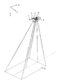
【図1】本発明の実施形態1である2次元走査装置の斜視図。
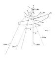
【図2】上記実施形態1の2次元走査装置の要部概要図。
【図3】2次元走査装置で用いられる1次元偏向器の要部概要図。
【図4】本発明の比較例1である2次元走査装置の水平断面図。
【図5】上記比較例1の2次元走査装置の数値例を示す表図。
【図6】TVディストーションおよび台形歪みを説明する図
【図7】上記比較例1における表示画像(格子)の説明図。
【図8】上記比較例1におけるTVディストーションと台形歪みの量を示す表図。
【図9】本発明の比較例2である2次元走査装置の水平断面図。
【図10】上記比較例2における表示画像(格子)の説明図。
【図11】上記比較例2におけるTVディストーションと台形歪みの量を示す表図。
【図12】上記実施形態1の2次元走査装置の水平断面図。
【図13】上記実施形態1の2次元走査装置の要部拡大図。
【図14】上記実施形態1の2次元走査装置の数値実施例を示す表図。
【図15】上記実施形態1における表示画像(格子)の説明図。
【図16】上記実施形態1におけるTVディストーションと台形歪みの量を示す表図。
【図17】本発明の実施形態2である2次元走査装置の水平断面図。
【図18】上記実施形態2の2次元走査装置の数値実施例を示す表図。
【図19】上記実施形態2における表示画像(格子)の説明図。
【図20】上記実施形態2におけるTVディストーションと台形歪みの量を示す表図。
【図21】本発明の実施形態3である2次元走査装置の水平断面図。
【図22】上記実施形態3の2次元走査装置の数値実施例を示す表図。
【図23】上記実施形態3における表示画像(格子)の説明図。
【図24】上記実施形態3におけるTVディストーションと台形歪みの量を示す表図。
【図25】本発明の実施形態4である2次元走査装置の水平断面図。
【図26】上記実施形態4の2次元走査装置の数値実施例を示す表図。
【図27】上記実施形態4における表示画像(格子)の説明図。
【図28】上記実施形態4におけるTVディストーションと台形歪みの量を示す表図。
【図29】本発明の実施形態5である2次元走査装置の水平断面図。
【図30】上記実施形態5の2次元走査装置の数値実施例を示す表図。
【図31】上記実施形態5における表示画像(格子)の説明図。
【図32】上記実施形態5におけるTVディストーションと台形歪みの量を示す表図。
【図33】2次元走査装置で用いられる2次元偏向器の要部概要図。
【図34】上記各実施形態の2次元走査装置を備えたプロジェクタを示す概略図。
【符号の説明】
1 光源
2 集光レンズ
3 開口絞り
4 偏向ユニット
5,15,25,35,45 走査光学系
6 被走査面[0001]
BACKGROUND OF THE INVENTION
The present invention relates to a two-dimensional scanning device used in a scanning image display device that displays a two-dimensional image by scanning light in a two-dimensional direction.
[0002]
[Prior art]
Various two-dimensional scanning devices that scan a light spot in a two-dimensional direction and form a two-dimensional image by the afterimage effect have been proposed.
[0003]
By the way, it is generally known that a so-called distortion is generated in a two-dimensional image on a surface to be scanned by deflecting and scanning the light beam two-dimensionally. Distortion includes trapezoidal distortion, constant-speed scanning distortion, straight-scanning distortion, and TV distortion that refers to the curvature of an image frame drawn on the surface to be scanned.
[0004]
In
[0005]
This is because TV distortion, which is image distortion that occurs when an image is formed by two-dimensional scanning of light, can be corrected by the f · sin θ characteristic of the scanning lens and electrical correction. .
[0006]
Further, in
[0007]
Although this is a two-dimensional scanning device configured using one optical element, the constant velocity of the scanning light on the surface to be scanned is well corrected over a wide scanning angle. It is also possible to achieve telecentricity necessary for high-precision drawing.
[0008]
[Patent Document 1]
JP-A-8-146320
[Patent Document 2]
JP 11-84291 A
[Patent Document 3]
Japanese Patent Laid-Open No. 2000-28183
[0009]
[Problems to be solved by the invention]
However, in the two-dimensional scanning apparatus proposed in
[0010]
Further, the two-dimensional scanning device proposed in
[0011]
Therefore, an object of the present invention is to provide a two-dimensional scanning apparatus that can easily and satisfactorily correct distortion including TV distortion and trapezoidal distortion.
[0012]
[Means for Solving the Problems]
In order to achieve the above object, a two-dimensional scanning device of the present invention includes a deflecting unit that deflects a light beam from a light source in a two-dimensional direction, and a light beam deflected by the deflecting unit is directed toward a surface to be scanned. From one or two lenses Scanning light system, and the light beam from the light source Orthogonal A scanning optical system that enters at least one of the deflection axes from an oblique direction. 1 lens or a lens on the side closer to the scanning surface among the 2 or less lenses The deflection means Immediately after reflecting An incident surface tilted so as to make an angle larger than the maximum field angle of the two-dimensional deflection range with respect to the central axis of the two-dimensional deflection range of the light beam, and an angle larger than the incident surface with respect to the central axis With tilted exit surface And Of the entrance and exit surfaces , Which is the center of each face The normal at the surface vertex One lens or near the surface to be scanned When extended to the exit side of the lens, it shifts to the side where the normal extends with respect to the central axis. The scanned surface is tilted in the same direction as the incident surface and the exit surface are tilted. It is characterized by being.
[0014]
Also, the tilted direction of the entrance surface and the exit surface is , the above Same as one of two orthogonal deflection axes You may do it.
[0019]
Also, above Entrance surface and exit surface In order to guide the light beam deflected by the deflecting means to the surface to be scanned. Entrance surface and exit surface Only the part on one side from the coordinate center (surface vertex) of may be used.
[0024]
Also, above Entrance surface and exit surface May be an anamorphic surface.
[0025]
Also, above Entrance surface and exit surface May be a rotationally asymmetric surface.
[0026]
Also, above lens May be a meniscus lens having a concave surface facing the deflecting means.
[0032]
Also, above Each of the two orthogonal deflection axes The angle of view in the direction is Different You may do it.
[0034]
Further, the light beam incident on the deflecting unit may be a convergent light beam.
[0035]
Further, the distortion on the scanned surface is scanning Optically corrected by the optical system or above scanning You may make it correct | amend by the combination of the optical correction by an optical system, and the electrical correction by the circuit which controls a deflection | deviation means.
[0036]
A scanning image display device such as an electronic viewfinder provided in a projector, a video camera, a digital still camera, or the like can be configured using the above two-dimensional scanning device.
[0037]
In this case, a color image may be formed on the surface to be scanned by causing a plurality of light beams having different wavelengths from the light source to enter the deflecting unit.
[0038]
DETAILED DESCRIPTION OF THE INVENTION
(Embodiment 1)
FIG. 1 shows the overall configuration of a two-dimensional scanning apparatus that is
[0039]
In these figures,
[0040]
[0041]
The light beam emitted from the
[0042]
[0043]
Here, FIG. A ) Shows a schematic configuration of the
[0044]
FIG. B ) Shows a schematic configuration of the
[0045]
The
[0046]
FIG. 4 shows a two-dimensional scanning apparatus as Comparative Example 1 used for comparison with the present embodiment. Horizontal A cross section (XZ cross section) is shown.
[0047]
In Comparative Example 1, as in the present embodiment, the divergent light beam emitted from the
[0048]
Here, a range in which the light beam is deflected in the two-dimensional direction by the
[0049]
In the first comparative example shown in FIG. 4, the deflection scanning axis Ldc and the optical axis of the scanning
[0050]
At this time, in the image drawn on the scanned
[0051]
A method for calculating TV distortion and trapezoidal distortion will be described with reference to FIGS.
[0052]
FIG. 6A is a diagram illustrating a method for calculating TV distortion. TV distortion is an amount of aberration that indicates the amount of curvature of the frame of the displayed image (screen), and is along an axis (horizontal axis, vertical axis) passing through the center of the image indicated by a dashed line in the figure. Displacement The amount is divided by the width of the image (horizontal width A, vertical width B). Therefore, the TV distortion at each side of the image frame is expressed by the following equation.
[0053]
Upper side L1; a / B × 100 (%)
Lower side L2; b / B × 100 (%)
Left side L3; c / A × 100 (%)
Right side L4; d / A × 100 (%)
FIG. 6B is a diagram for explaining a method for calculating the trapezoidal distortion. Trapezoidal distortion is the amount of aberration that indicates the amount by which the frame of the displayed image is tilted. Displacement The amount divided by the width of the image. Therefore, the trapezoidal distortion at each side of the image frame is expressed by the following equation.
[0054]
Upper side L1; e / 2 / B × 100 (%)
Lower side L2; f / 2 / B × 100 (%)
Left side L3; g / 2 / A × 100 (%)
Right side L4; h / 2 / A × 100 (%)
FIG. 7 shows an image (lattice) scanned and displayed by the two-dimensional scanning device of Comparative Example 1. FIG. 8 shows the amount of TV distortion and trapezoidal distortion in the display image.
[0055]
As shown in FIG. 7, the four lines (sides) constituting the frame of the image should ideally all be straight lines, but the upper side L1 and the lower side L2 of the frame are substantially straight lines. It can be seen that the central portions of the left side L3 and the right side L4 are curves that are recessed toward the center of the image, and that a large amount of TV distortion occurs. At this time, the TV distortion was 0.12 (%) on the upper side, 0.12 (%) on the lower side, 1.53 (%) on the left side, and 1.53 (%) on the right side (see FIG. 8). In Comparative Example 1, since the scanning
[0056]
As described above, in a general optical arrangement in which the optical axis of the scanning
[0057]
FIG. 9 shows the two-dimensional scanning device in Comparative Example 2. Horizontal A cross section (XZ cross section) is shown. In Comparative Example 2, the scanning
[0058]
In particular, Horizontal The orientation and position of the
[0059]
Thus, on the optical axis of each
[0060]
FIG. 10 shows an image (lattice) scanned and displayed by the two-dimensional scanning device of Comparative Example 2. FIG. 11 shows the amount of TV distortion and trapezoidal distortion in the display image.
[0061]
In Comparative Example 2, as shown in FIG. 10, TV distortion occurs asymmetrically in the left-right direction (horizontal direction). That is, on the left side where the deflected light beam passes near the optical axis of the
[0062]
As shown in FIG. 11, the TV distortion was 0.90 (%) on the upper side, 0.90 (%) on the lower side, 0.00 (%) on the left side, and 1.70 (%) on the right side (see FIG. 11). The trapezoidal distortion was 1.02 (%) on the upper side, 1.02 (%) on the lower side, 0.00 (%) on the left side, and 0.00 (%) on the right side (see FIG. 11).
[0063]
Also in the comparative example 2, TV distortion and trapezoidal distortion are greatly generated, and the quality of the display image is deteriorated.
[0064]
Therefore, in the present embodiment, the arrangement of the scanning
[0065]
FIG. 12 shows the two-dimensional scanning apparatus according to
[0066]
Hereinafter, the arrangement of the scanning
[0067]
The scanning
[0068]
In the present embodiment, the maximum horizontal field angle α is ± 20.3 (deg) centered on the deflection scanning axis Ldc, and the maximum vertical field angle is ± 15.2 (deg) centered on the deflection scanning axis Ldc.
[0069]
First, the scanning
[0070]
The
[0071]
On the other hand, the
[0072]
The
[0073]
Therefore, the surface vertex of the incident surface of the
[0074]
Furthermore, in this embodiment, Horizontal In the cross section, the scanned surface 6 (normal line thereof) is tilted by γ ′ = 10.1 (deg) in the counterclockwise direction in FIG. 12 with respect to the deflected light beam Bdm having the maximum angle of view α. Γ = 30.4 (deg) is tilted with respect to the deflection scanning axis Ldc. At this time, the scanned
[0075]
The two
[0076]
In the rotationally asymmetric aspherical surface in the present embodiment, the displacement amount Z in the direction in which the deflected light beam Bdm travels (Z direction) is expressed by the following equation at each position in the horizontal direction (X direction) and the vertical direction (Y direction). It has a shape.
[0077]
[Formula 1]
Where z: sag of plane parallel to Z-axis
c: curvature of vertex
k: Conic coefficient
Cj: coefficient of xmyn
It is.
[0079]
FIG. 15 shows an image (lattice) scanned and displayed by the two-dimensional scanning device of the present embodiment. FIG. 16 shows the amount of TV distortion and trapezoidal distortion of the display image.
[0080]
In the TV distortion of the image shown in FIG. 15, the upper side L1 of the frame is 0.15 (%), the lower side L2 is 0.15 (%), the left side L3 is 0.27 (%), and the right side L4 is 0.04 (%). %) And In the comparative example The curved upper side L1 and lower side L2 are corrected to be substantially straight lines. Further, the trapezoidal distortion is such that the upper side L1 and the lower side L2 are both 0.05 (%), the left side L3 and the right side L4 are both 0 (%), and In the comparative example The inclined line is corrected to a vertical line.
[0081]
As described above, according to this embodiment, the optical axis of the scanning
[0082]
Specifically, at least one optical element (
[0083]
Here, a TV distortion correction mechanism will be described. By displacing the scanning optical system (
[0084]
That is, the scanning
[0085]
In other words, the TV optical distortion is generated asymmetrically by shifting the scanning
[0086]
Next, the correction mechanism for trapezoidal distortion will be described. Although the trapezoidal distortion is generated by decentering the scanning optical system 5 (
[0087]
As described above, according to the present embodiment, it is possible to realize a two-dimensional scanning device that can satisfactorily correct TV distortion and trapezoidal distortion generated in a display image formed on the scanned
[0088]
Note that, when the two-dimensional scanning device of the present embodiment is used as a projector, it is possible to project an image from an oblique direction onto a projection surface such as a screen by tilting the
[0089]
In the present embodiment, the tilted second scanning lens (transmission type optical element having no reflecting surface) 5b has a meniscus shape with a concave surface facing the
[0090]
In addition, the optical surfaces of the two optical elements constituting the scanning
[0091]
Furthermore, since the transmittance of light rays for displaying an image is higher than the reflectance, there is also a merit that the loss of light amount is very small, especially when the number of optical surfaces is large. Further, the transmittance is very high by applying the antireflection film.
[0092]
In addition, in an optical element in which a refracting surface and a reflecting surface are mixed, it is necessary to secure an optical path inside the optical element, and the optical element itself becomes large.
[0093]
However, in the case of using an optical element whose optical surface is composed only of a refracting surface, it is not necessary to secure an optical path in the optical element, so that the optical element can be thinned and the two-dimensional scanning apparatus can be miniaturized. It is advantageous.
[0094]
Therefore, when an optical element that does not have a reflecting surface that directs light to the surface to be scanned is used in the scanning optical system, the reflecting surface is proposed as disclosed in Japanese Patent Laid-Open Nos. 11-84291 and 2001-28183. Compared to the use of an optical member having the above, various effects can be enjoyed. In the present invention, an optical element that uses a diffractive surface that transmits and diffracts light instead of the refracting surface or in combination with the refracting surface can also be used to correct image distortion on the surface to be scanned.
[0095]
In the present embodiment, the two optical elements constituting the scanning
[0096]
(Embodiment 2)
FIG. 17 shows a two-dimensional scanning device according to
[0097]
This embodiment is different from the first embodiment in that the light beam incident on the
[0098]
As in the first embodiment, the scanning
[0099]
The scanning
[0100]
On the other hand, the
[0101]
Further, the
[0102]
The scanned
[0103]
In the scanning
[0104]
Further, the exit surface of the
[0105]
FIG. 19 shows an image (grating) scanned and displayed by the two-dimensional scanning apparatus of this embodiment, and FIG. 20 shows the amount of TV distortion and trapezoidal distortion of the display image.
[0106]
The TV distortion is 0.16 (%) on the upper side L1 of the image frame, 0.16 (%) on the lower side L2, 0.19 (%) on the left side L3, and 0.11 (%) on the right side L4, and is corrected well. The trapezoidal distortion is 0.11 (%) for both the upper side L1 and the lower side L2 of the image frame, and 0.0 (%) for both the left side L3 and the right side L4.
[0107]
As described above, the
[0108]
An object of the present invention is to provide a two-dimensional scanning device that can always display a high-quality image. TV distortion is an aberration amount indicating the linearity of the frame of the display image, but in order to display a high-quality image, it is necessary to properly correct the linearity at a position inside the frame of the display image. . However, in general, the linearity generated differs depending on the position and direction of the image, and even if the scanning optical system is tilted or shifted, the inside of the frame may not be completely corrected.
[0109]
Therefore, in the present embodiment, the
[0110]
The
[0111]
In this embodiment, an aspherical coefficient up to (m + n) ≦ 4 is used for the rotationally asymmetric aspherical surface of the tilted or shifted
[0112]
Further, as in this embodiment, the two-dimensional scanning apparatus can be made compact by cutting the other portions of the lens that is tilted and shifted while leaving only the portion to be used.
[0113]
(Embodiment 3)
FIG. 21 shows a two-dimensional scanning apparatus according to
[0114]
In the present embodiment, the two optical elements (25a, 25b) constituting the scanning
[0115]
Also in the present embodiment, as in the second embodiment, the scanning
[0116]
The
[0117]
The
[0118]
Further, when the normal line of the surface vertex of the incident surface is extended to the output side, the
[0119]
Therefore, all optical surfaces (incident / exit surfaces) of all optical elements (
[0120]
At this time, the
[0121]
The scanned
[0122]
FIG. 23 shows an image (lattice) scanned and displayed by the two-dimensional scanning apparatus of this embodiment, and FIG. 24 shows the amount of TV distortion and trapezoidal distortion of the display image.
[0123]
The TV distortion is 0.04 (%) at the upper side L1 of the image frame, 0.04 (%) at the lower side L2, 0.06 (%) at the left side L3, and 0.11 (%) at the right side L4, and is corrected very well. The trapezoidal distortion is 0.01% for both the upper side L1 and the lower side L2 of the image frame, and 0.00% for both the left side L3 and the right side L4, and is corrected so that the trapezoidal distortion is almost eliminated.
[0124]
As described above, by arranging two or more optical elements of the optical elements included in the scanning optical system outside the two-dimensional deflection range in which the deflected light beam is deflected, the effect of correcting TV distortion and trapezoidal distortion is increased. . Therefore, it is possible to realize a two-dimensional scanning apparatus capable of displaying a very high-quality two-dimensional image.
[0125]
In the present embodiment, the
[0126]
(Embodiment 4)
FIG. 25 shows a two-dimensional scanning apparatus according to
[0127]
This embodiment is different from
[0128]
Also in the present embodiment, as in the second embodiment, the scanning
[0129]
The
[0130]
Further, the
[0131]
The
[0132]
Further, the
[0133]
Thus, in this embodiment, the two optical elements (35a, 35b) included in the scanning
[0134]
Each of these configurations has an effect of satisfactorily correcting TV distortion. By adopting a configuration in which these are combined into one, TV distortion can be corrected extremely well.
[0135]
FIG. 27 shows an image (lattice) scanned and displayed by the two-dimensional scanning apparatus of this embodiment, and FIG. 28 shows the amount of TV distortion and trapezoidal distortion of the display image.
[0136]
The TV distortion is 0.06 (%) on the upper side L1 of the image frame, 0.06 (%) on the lower side L2, 0.07 (%) on the left side L3, and 0.06 (%) on the right side L4, and is corrected very well. The trapezoidal distortion is 0.01 (%) for both the upper side L1 and the lower side L2 of the frame of the image, and 0.00 (%) for both the left side L3 and the right side L4, and is corrected so that the trapezoidal distortion is almost eliminated.
[0137]
In this way, by tilting two or more of the optical elements included in the scanning optical system at an angle larger than the maximum field angle with respect to the deflection scanning axis, the effect of correcting TV distortion and trapezoidal distortion can be obtained. Can be improved. Further, by making the tilt amount and the shift amount different for each optical surface of each optical element, it is possible to further enhance the effect of correcting TV distortion and trapezoidal distortion. Therefore, it is possible to realize a two-dimensional scanning device capable of displaying a very high-quality two-dimensional image.
[0138]
In this embodiment, two optical elements are tilted and shifted. However, the present invention is not limited to this. For example, the same effect can be obtained by tilting or shifting three or more optical elements. Can do.
[0139]
(Embodiment 5)
FIG. 29 shows a two-dimensional scanning apparatus according to
[0140]
This embodiment is different from the other embodiments in that the scanning
[0141]
The scanning
[0142]
Further, the exit surface of the
[0143]
Further, when the surface normal of the incident surface is extended to the exit side, the
[0144]
Further, the scanned
[0145]
Thus, in the present embodiment, since the scanning
[0146]
Further, in the present embodiment, the
[0147]
FIG. 31 shows an image (grating) scanned and displayed by the two-dimensional scanning apparatus of this embodiment, and FIG. 32 shows the amount of TV distortion and trapezoidal distortion of the display image.
[0148]
The TV distortion is 0.17 (%) on the upper side L1 of the image, 0.17 (%) on the lower side L2, 0.13 (%) on the left side L3, and 0.20 (%) on the right side L4, and is sufficiently corrected. The trapezoidal distortion is 0.10 (%) for both the upper side L1 and the lower side L2, and is 0.00 (%) for both the left side L3 and the right side L4.
[0149]
As described above, even when the scanning
[0150]
Furthermore, a rotationally asymmetric aspherical surface is used for the tilting optical element, the surface apex of the optical element is arranged outside the two-dimensional deflection range where the deflected light beam is deflected, and the tilt amount and shift amount of each optical surface of the optical element are set. By making them different from each other, the effect of correcting TV distortion and trapezoidal distortion can be remarkably improved.
[0151]
In each of the above embodiments, the case where a glass lens is used as an optical element constituting the scanning optical system has been described. However, by using an optical element other than a glass lens, for example, a plastic lens made by injection molding, manufacturing is performed. Thus, the cost can be reduced and the weight of the two-dimensional scanning device can be reduced.
[0152]
Further, a two-dimensional color image can be displayed by providing the light source with light emitting portions of three colors of blue, green, and red. In this case, achromatization may be performed using an optical element including a diffraction grating. Accordingly, it is possible to realize a scanning image display device that can scan and display a high-quality color image. In this case, for example, light of three colors of blue, green, and red may be directed to the deflection unit sequentially (field sequential) or simultaneously. In addition to this, a combination of a white light source and blue, green, and red filters arranged on a rotatable turret allows the blue, green, and red light to be sequentially applied to the deflection unit. Can be directed.
[0153]
As described above, the light source and the deflection unit control method for forming a color two-dimensional image using the deflection unit and the scanning optical system while directing light of three colors of blue, green, and red from the light source to the deflection unit. Description is omitted.
[0154]
In each of the above embodiments, the case where two deflectors using MEMS devices capable of resonant oscillation in a one-dimensional direction are provided as the deflection unit has been described. However, the MEMS device shown in FIG. May be used. In the deflector using the MEMS device, the reflecting
[0155]
Further, instead of the deflector using the MEMS device, a galvanometer mirror or polygon mirror whose reflecting surface rotates may be used.
[0156]
Further, as proposed in the above-mentioned Japanese Patent Laid-Open No. 8-146320, there is a technique for electrically correcting TV distortion. However, this kind of electrical correction and optical by the scanning optical system according to the present invention are also available. It is also possible to adopt a configuration in which image distortion is corrected by combining various corrections.
[0157]
When the TV distortion is electrically corrected, a drive circuit (not shown) that controls the deflection means controls the tilt angle of the reflecting surface during two-dimensional scanning so as to correct the remaining distortion after optical correction.
[0158]
(Sixth embodiment)
FIG. 34 shows an example of a scanning image display device provided with the two-dimensional scanning device of the present embodiment. FIG. 34A shows a
[0159]
FIG. 34B shows a stand-
[0160]
Both
[0161]
Each of the embodiments described above has been described by taking an example of an image display device (for example, a projector) that has a screen or the like on the surface to be scanned and directly observes the image. The present invention can also be applied to an image display device (for example, a finder) that is observed through a relay optical system or the like.
[0162]
Furthermore, the present invention can also be applied to the case where the light beam from the light source is incident on the reflecting surface of the deflecting means from an oblique direction with respect to the swing axis (deflection axis) of the reflecting surface.
[0163]
【The invention's effect】
As described above, according to the present invention, it is possible to easily and satisfactorily correct TV distortion and distortion including trapezoidal distortion that occur when a light beam is deflected and scanned in a two-dimensional direction to form a two-dimensional image. Thereby, it is possible to realize a two-dimensional scanning device and a scanning image display device capable of displaying a high-quality image with little distortion.
[Brief description of the drawings]
FIG. 1 is a perspective view of a two-dimensional scanning apparatus that is
FIG. 2 is a schematic diagram of a main part of the two-dimensional scanning apparatus according to the first embodiment.
FIG. 3 is a schematic diagram of a main part of a one-dimensional deflector used in a two-dimensional scanning device.
FIG. 4 shows a two-dimensional scanning apparatus according to Comparative Example 1 of the present invention. Horizontal Sectional drawing.
FIG. 5 is a table showing numerical examples of the two-dimensional scanning device of Comparative Example 1;
FIG. 6 is a diagram for explaining TV distortion and trapezoidal distortion.
FIG. 7 is an explanatory diagram of a display image (lattice) in the comparative example 1;
FIG. 8 is a table showing the amount of TV distortion and trapezoidal distortion in Comparative Example 1;
FIG. 9 shows a two-dimensional scanning apparatus according to Comparative Example 2 of the present invention. Horizontal Sectional drawing.
10 is an explanatory diagram of a display image (lattice) in the comparative example 2. FIG.
FIG. 11 is a table showing the amount of TV distortion and trapezoidal distortion in Comparative Example 2;
FIG. 12 shows the two-dimensional scanning apparatus according to the first embodiment. Horizontal Sectional drawing.
FIG. 13 is an enlarged view of a main part of the two-dimensional scanning device according to the first embodiment.
FIG. 14 is a table showing numerical examples of the two-dimensional scanning apparatus according to the first embodiment.
15 is an explanatory diagram of a display image (grid) in the first embodiment. FIG.
FIG. 16 is a table showing the amount of TV distortion and trapezoidal distortion in the first embodiment.
FIG. 17 shows a two-dimensional scanning apparatus according to
FIG. 18 is a table showing a numerical example of the two-dimensional scanning device according to the second embodiment.
FIG. 19 is an explanatory diagram of a display image (grid) in the second embodiment.
FIG. 20 is a table showing the amount of TV distortion and trapezoidal distortion in the second embodiment.
FIG. 21 shows a two-dimensional scanning apparatus according to
FIG. 22 is a table showing numerical examples of the two-dimensional scanning device according to the third embodiment.
FIG. 23 is an explanatory diagram of a display image (grid) in the third embodiment.
FIG. 24 is a table showing the amount of TV distortion and trapezoidal distortion in the third embodiment.
FIG. 25 shows a two-dimensional scanning apparatus according to
FIG. 26 is a table showing numerical examples of the two-dimensional scanning device according to the fourth embodiment.
FIG. 27 is an explanatory diagram of a display image (grid) in the fourth embodiment.
FIG. 28 is a table showing the amount of TV distortion and trapezoidal distortion in the fourth embodiment.
FIG. 29 shows a two-dimensional scanning apparatus according to
FIG. 30 is a table showing numerical examples of the two-dimensional scanning device according to the fifth embodiment.
FIG. 31 is an explanatory diagram of a display image (grid) in the fifth embodiment.
FIG. 32 is a table showing the amount of TV distortion and trapezoidal distortion in the fifth embodiment.
FIG. 33 is a main part schematic diagram of a two-dimensional deflector used in a two-dimensional scanning apparatus.
FIG. 34 is a schematic diagram showing a projector provided with the two-dimensional scanning device of each of the embodiments.
[Explanation of symbols]
1 Light source
2 Condensing lens
3 Aperture stop
4 Deflection unit
5, 15, 25, 35, 45 Scanning optical system
6 Surface to be scanned
Claims (10)
前記偏向手段により偏向された光束を被走査面に向け、1枚または2枚のレンズからなる走査光学系とを有し、
前記光源からの光束が、前記偏向手段における2つの直交する偏向軸のうち少なくとも一方に対して斜め方向から入射し、
前記走査光学系の1枚のレンズ、または2枚以内のレンズのうち被走査面に近い側のレンズは、前記偏向手段を反射した直後の光束の2次元偏向範囲の中心軸に対して前記2次元偏向範囲の最大画角よりも大きな角度をなすようにチルトした入射面と、前記中心軸に対して前記入射面よりも大きな角度をなすようにチルトした出射面とを有し、
かつ前記入射面及び前記出射面の、それぞれの面の中心である面頂点における法線を前記1枚のレンズまたは被走査面に近い側のレンズの出射側に延ばしたときに、前記中心軸に対して前記法線が延びる側にシフトしており、
被走査面は前記入射面及び前記出射面がチルトしている方向と同一方向にチルトしていることを特徴とする2次元走査装置。Deflecting means for deflecting the light beam from the light source in a two-dimensional direction;
Wherein the light beam deflected by the deflecting means toward the surface to be scanned, and a one or two Ru scanning optical system name from the lens,
The light beam from the light source is incident on at least one of the two orthogonal deflection axes in the deflection unit from an oblique direction,
One lens of the scanning optical system , or a lens closer to the scanning surface among the two or less lenses, is 2 with respect to the central axis of the two-dimensional deflection range of the light beam immediately after being reflected by the deflecting means. possess an entrance surface which is tilted to form an angle larger than the maximum angle dimension deflection range, an exit surface which is tilted to form an angle larger than the incident surface to the central axis,
And when the normal line at the surface vertex that is the center of each of the entrance surface and the exit surface is extended to the exit side of the one lens or the lens close to the scanned surface , In contrast, the normal is shifted to the extending side ,
The two-dimensional scanning apparatus characterized in that the surface to be scanned is tilted in the same direction as the direction in which the incident surface and the exit surface are tilted .
前記偏向手段により偏向された光束を前記被走査面に導光するために、前記入射面及び前記出射面の面頂点から片側の部分のみが使用されることを特徴とする請求項1又は2に記載の2次元走査装置。Surface vertices of the entrance surface and the exit surface are located outside the two-dimensional deflection range;
3. The method according to claim 1, wherein only a portion on one side of the incident surface and the exit surface is used to guide the light beam deflected by the deflecting unit to the surface to be scanned. The two-dimensional scanning device described.
Priority Applications (2)
| Application Number | Priority Date | Filing Date | Title |
|---|---|---|---|
| JP2002302385A JP4174288B2 (en) | 2002-10-16 | 2002-10-16 | Two-dimensional scanning device and scanning image display device |
| US10/686,396 US7554710B2 (en) | 2002-10-16 | 2003-10-14 | Two-dimensional scanning apparatus, and image displaying apparatus |
Applications Claiming Priority (1)
| Application Number | Priority Date | Filing Date | Title |
|---|---|---|---|
| JP2002302385A JP4174288B2 (en) | 2002-10-16 | 2002-10-16 | Two-dimensional scanning device and scanning image display device |
Publications (3)
| Publication Number | Publication Date |
|---|---|
| JP2004138748A JP2004138748A (en) | 2004-05-13 |
| JP2004138748A5 JP2004138748A5 (en) | 2005-11-04 |
| JP4174288B2 true JP4174288B2 (en) | 2008-10-29 |
Family
ID=32450452
Family Applications (1)
| Application Number | Title | Priority Date | Filing Date |
|---|---|---|---|
| JP2002302385A Expired - Fee Related JP4174288B2 (en) | 2002-10-16 | 2002-10-16 | Two-dimensional scanning device and scanning image display device |
Country Status (1)
| Country | Link |
|---|---|
| JP (1) | JP4174288B2 (en) |
Families Citing this family (5)
| Publication number | Priority date | Publication date | Assignee | Title |
|---|---|---|---|---|
| JP5050862B2 (en) * | 2008-01-09 | 2012-10-17 | 株式会社デンソー | Image forming apparatus |
| CN102132191B (en) | 2008-08-21 | 2012-10-17 | 柯尼卡美能达精密光学株式会社 | Laser projector |
| WO2010035330A1 (en) | 2008-09-26 | 2010-04-01 | Hoya株式会社 | Scanning optical device |
| US8992028B2 (en) * | 2011-04-14 | 2015-03-31 | Microvision, Inc. | Free form optical redirection apparatus and devices using same |
| US9798138B2 (en) | 2015-01-30 | 2017-10-24 | Canon Kabushiki Kaisha | Optical scanning device, image forming apparatus, and imaging optical element |
-
2002
- 2002-10-16 JP JP2002302385A patent/JP4174288B2/en not_active Expired - Fee Related
Also Published As
| Publication number | Publication date |
|---|---|
| JP2004138748A (en) | 2004-05-13 |
Similar Documents
| Publication | Publication Date | Title |
|---|---|---|
| JP4522253B2 (en) | Optical scanning device and image display device using the same | |
| JP5304380B2 (en) | Optical scanning device, image projection device using the same, head-up display device, and mobile phone | |
| US7385745B2 (en) | Two-dimensional scanning apparatus and scanning type image displaying apparatus using the same | |
| US7605775B2 (en) | Displaying optical system | |
| JP4266660B2 (en) | Projection type display optical system and projection type image display device | |
| JP4372891B2 (en) | Video display device | |
| JP4006313B2 (en) | Scanning display optical system and scanning display device | |
| US7880948B2 (en) | Scanning projection device | |
| US7554710B2 (en) | Two-dimensional scanning apparatus, and image displaying apparatus | |
| JPH1184291A (en) | Scanning optical system | |
| JP4574774B2 (en) | Video display device | |
| JP6740360B2 (en) | Projection optical system and head-up display device | |
| JP4174288B2 (en) | Two-dimensional scanning device and scanning image display device | |
| US7183539B2 (en) | Optical system for displaying image and image display apparatus | |
| US6859329B2 (en) | Scanning type display optical system and scanning type image display apparatus | |
| JPWO2009057522A1 (en) | Scanning projector | |
| JP4174287B2 (en) | Two-dimensional scanning device and image display device | |
| JP4033122B2 (en) | Optical scanner and image forming apparatus having the same | |
| JP2010008735A (en) | Scanning type image projector | |
| JP4533409B2 (en) | Scanning display optical system | |
| JP2001141913A (en) | Image rotating prism and stereographic image display device using the prism |
Legal Events
| Date | Code | Title | Description |
|---|---|---|---|
| A521 | Written amendment |
Free format text: JAPANESE INTERMEDIATE CODE: A523 Effective date: 20050808 |
|
| A621 | Written request for application examination |
Free format text: JAPANESE INTERMEDIATE CODE: A621 Effective date: 20050808 |
|
| A977 | Report on retrieval |
Free format text: JAPANESE INTERMEDIATE CODE: A971007 Effective date: 20070518 |
|
| A131 | Notification of reasons for refusal |
Free format text: JAPANESE INTERMEDIATE CODE: A131 Effective date: 20070605 |
|
| A521 | Written amendment |
Free format text: JAPANESE INTERMEDIATE CODE: A523 Effective date: 20070806 |
|
| A131 | Notification of reasons for refusal |
Free format text: JAPANESE INTERMEDIATE CODE: A131 Effective date: 20070911 |
|
| A521 | Written amendment |
Free format text: JAPANESE INTERMEDIATE CODE: A523 Effective date: 20071112 |
|
| A02 | Decision of refusal |
Free format text: JAPANESE INTERMEDIATE CODE: A02 Effective date: 20071225 |
|
| A521 | Written amendment |
Free format text: JAPANESE INTERMEDIATE CODE: A523 Effective date: 20080225 |
|
| A911 | Transfer of reconsideration by examiner before appeal (zenchi) |
Free format text: JAPANESE INTERMEDIATE CODE: A911 Effective date: 20080306 |
|
| A131 | Notification of reasons for refusal |
Free format text: JAPANESE INTERMEDIATE CODE: A131 Effective date: 20080507 |
|
| RD13 | Notification of appointment of power of sub attorney |
Free format text: JAPANESE INTERMEDIATE CODE: A7433 Effective date: 20080513 |
|
| A521 | Written amendment |
Free format text: JAPANESE INTERMEDIATE CODE: A821 Effective date: 20080513 |
|
| A521 | Written amendment |
Free format text: JAPANESE INTERMEDIATE CODE: A523 Effective date: 20080624 |
|
| TRDD | Decision of grant or rejection written | ||
| A01 | Written decision to grant a patent or to grant a registration (utility model) |
Free format text: JAPANESE INTERMEDIATE CODE: A01 Effective date: 20080722 |
|
| A01 | Written decision to grant a patent or to grant a registration (utility model) |
Free format text: JAPANESE INTERMEDIATE CODE: A01 |
|
| A61 | First payment of annual fees (during grant procedure) |
Free format text: JAPANESE INTERMEDIATE CODE: A61 Effective date: 20080818 |
|
| R150 | Certificate of patent or registration of utility model |
Ref document number: 4174288 Country of ref document: JP Free format text: JAPANESE INTERMEDIATE CODE: R150 Free format text: JAPANESE INTERMEDIATE CODE: R150 |
|
| FPAY | Renewal fee payment (event date is renewal date of database) |
Free format text: PAYMENT UNTIL: 20110822 Year of fee payment: 3 |
|
| FPAY | Renewal fee payment (event date is renewal date of database) |
Free format text: PAYMENT UNTIL: 20120822 Year of fee payment: 4 |
|
| FPAY | Renewal fee payment (event date is renewal date of database) |
Free format text: PAYMENT UNTIL: 20120822 Year of fee payment: 4 |
|
| FPAY | Renewal fee payment (event date is renewal date of database) |
Free format text: PAYMENT UNTIL: 20130822 Year of fee payment: 5 |
|
| LAPS | Cancellation because of no payment of annual fees |