JP4158564B2 - Synchronous transmission system - Google Patents
Synchronous transmission system Download PDFInfo
- Publication number
- JP4158564B2 JP4158564B2 JP2003069938A JP2003069938A JP4158564B2 JP 4158564 B2 JP4158564 B2 JP 4158564B2 JP 2003069938 A JP2003069938 A JP 2003069938A JP 2003069938 A JP2003069938 A JP 2003069938A JP 4158564 B2 JP4158564 B2 JP 4158564B2
- Authority
- JP
- Japan
- Prior art keywords
- signal
- node
- time
- transmission system
- synchronous transmission
- Prior art date
- Legal status (The legal status is an assumption and is not a legal conclusion. Google has not performed a legal analysis and makes no representation as to the accuracy of the status listed.)
- Expired - Fee Related
Links
- 230000005540 biological transmission Effects 0.000 title claims description 69
- 230000001360 synchronised effect Effects 0.000 title claims description 26
- 238000006243 chemical reaction Methods 0.000 claims description 29
- 230000008054 signal transmission Effects 0.000 claims description 27
- 238000012360 testing method Methods 0.000 claims description 15
- 230000003287 optical effect Effects 0.000 claims description 10
- 238000012545 processing Methods 0.000 claims description 8
- 230000015654 memory Effects 0.000 description 56
- 238000010586 diagram Methods 0.000 description 13
- 238000000034 method Methods 0.000 description 9
- 238000012546 transfer Methods 0.000 description 5
- 238000007796 conventional method Methods 0.000 description 3
- 238000001514 detection method Methods 0.000 description 3
- 239000004065 semiconductor Substances 0.000 description 3
- 230000000630 rising effect Effects 0.000 description 2
- 230000004913 activation Effects 0.000 description 1
- 230000003111 delayed effect Effects 0.000 description 1
- 230000000694 effects Effects 0.000 description 1
Images
Landscapes
- Optical Communication System (AREA)
- Information Transfer Systems (AREA)
- Dc Digital Transmission (AREA)
- Synchronisation In Digital Transmission Systems (AREA)
Description
【0001】
【発明の属する技術分野】
本発明は、CPUメモリバスのような高速かつ低レンテンシを要求される伝送路を介して複数のノード間で信号伝送を行うための同期伝送システムに関する。
【0002】
【従来の技術】
CPUの動作周波数は半導体技術の進歩により向上してきたが、CPUの動作周波数に比べると、CPUメモリ間の信号伝送周波数は一桁低く、CPUメモリシステム全体の性能ボトルネックとなっている。一般には伝送路の帯域を向上する方法として、シリアル伝送が知られている。これは複数の信号を並列直列変換により速度変換した後に送信し、受信側にて直列並列変換を施して元の複数の信号を得る方法である。
【0003】
しかしCPUメモリ間のデータ転送においては、帯域向上だけでなく両者間のデータ転送遅延時間、いわゆるレイテンシの低減が必要である。上述のシリアル伝送は従来方法に加えて並列直列変換、および直列並列変換に要する時間分のレイテンシが増大する問題があった。
【0004】
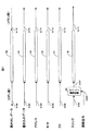
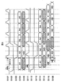
図3は、従来の同期伝送システムの一例を示す図である。このシステムは、1つのCPUと1つのメモリ間を伝送路30〜35で接続したものである。図示のように、CPU側からクロック信号S101、チップセレクト(CS)信号S102、書き込み/読み出し(R/W)信号S103、アドレス信号S104、および書き込みデータ信号S105が、伝送路30〜34を介して伝送され、メモリ側でそれぞれ対応する信号S111、S112、S113、S114、S115として受信される。一方、メモリ側からは、読み出しデータ信号S116が伝送路35を介して伝送され、CPU側で信号S106として受信される。
【0005】
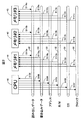
図4は、図3のシステムにおけるタイミングチャートを示す図である。図のように、CPUから出力される信号S102〜S105は、いずれもデューティ50%であるクロック信号S101の立ち上がりエッジに同期して出力される。R/W信号S103は、値”1”が読み出し、値”0”が書き込み指示を表す。CS信号S102は、値”0”が有効とする。図4中の記号dはCPUとメモリ間の信号伝送時間を表す。以下では信号伝送時間dは、あるノードから他のノードへの信号伝送に要する時間を表し、ノード間に存在する伝送路や回路部品の伝播遅延時間、更にラッチ回路を通過する際に生じる同期信号の待ち時間等を全て含む。但し図4におけるdは伝送路30〜35の伝播遅延時間に相当する。図4の最初の一周期は読み出し動作を表し、メモリアドレスA1からデータRDを読み出す。ここではメモリ側で受信するクロック信号S111の立下りエッジから、時間rだけ経過後に読み出しデータ信号S116が確定するものとする。図中の記号sはCPU側のデータ信号のセットアップ時間を示す。このシステムの場合、レイテンシの下限L0と動作周波数の上限F0は以下のようになる。
L0=max(d,2d+r+s)×2=4d+2r+2s、F0=1/L0
【0006】
なお、入力クロック信号に基づき所望のデューティを持つクロック信号を生成するクロック生成回路および当該クロック生成回路により生成されたクロック信号で動作タイミングを制御する半導体記憶装置が特許文献1に記載されているが、この技術はメモリ内における異なる動作間の衝突を回避するためのものであり、CPUメモリバス等におけるレイテンシの問題を解決するものではない。
【特許文献1】
特開2000−99194号公報
【0007】
【発明が解決しようとする課題】
従って本発明の目的は、データ転送におけるレイテンシを低減し、かつ伝送帯域を向上し得る同期伝送システムを提供することにある。
【0008】
【課題を解決するための手段】
上記目的は、第1のクロック信号の出力手段とデータ信号の入力手段および/または出力手段を備える第1のノードと、第2のクロック信号の入力手段とデータ信号の入力手段および/または出力手段を備える第2のノードとの間で伝送路を介して信号伝送を行うための同期伝送システムであって、前記第1のノードおよび/または前記第2のノードが前記第1のクロック信号および/または前記第2のクロック信号のデューティ比を調整信号に従って変更するデューティ調整回路を備えた同期伝送システムにより、達成される。
【0009】
ここで、前記調整信号は、前記第1のノードから前記第2のノードへの信号伝送時間と、前記第2のノードから前記第1のノードへの信号伝送時間と、前記第2のノードにおけるデータ信号の入力から出力に至るまでの処理時間とに基づいて生成することができる。また、本同期伝送システムは、複数の前記第1のノードおよび/または複数の前記第2のノードを備えることができる。この場合、前記調整信号は、前記各第1のノードから前記各第2のノードへの信号伝送時間の最大値と、前記各第2のノードから前記各第1のノードへの信号伝送時間の最大値と、前記各第2のノードにおけるデータ信号の入力から出力に至るまでの処理時間の最大値とに基づいて生成することができる。
【0010】
また、前記第1のノードはテスト信号を前記第2のノードへ送信し、前記第2のノードは前記テスト信号を前記第1のノードに返信し、前記テスト信号と前記返信されたテスト信号との時間差より前記信号伝送時間を算出することができる。前記テスト信号は、システムの電源投入直後および/または前記伝送路の未使用時間に送信することができる。
【0011】
さらに、前記出力手段は電気信号を光信号に変換する電気光変換手段を備え、前記入力手段は光信号を電気信号に変換する光電気変換手段を備え、前記電気光変換手段と前記光電気変換手段との間を光伝送路により光学的に接続することができる。前記信号伝送時間は、前記電気光変換手段における電気光変換時間および前記光電気変換手段における光電気変換時間を含むことができる。
このように構成することにより、データ転送におけるレイテンシを低減し、かつ伝送帯域を向上することができる。
【0012】
【発明の実施の形態】
図1は、本発明に係る同期伝送システムの一実施例を示す図である。本実施例は、1つのCPUと1つのメモリ間を伝送路30〜35で接続した例を示しており、CPU側に調整信号S200によりクロック信号のデューティ比を変更可能なデューティ調整回路20を備える。この調整信号S200は、例えば、CPUからメモリへの信号伝送時間と、メモリからCPUへの信号伝送時間と、メモリにおけるデータ信号の入力から出力に至るまでの処理時間とに基づいて生成することができる。調整信号の生成の仕方ついては後述する。
【0013】
図1において、CPU側のクロック信号S101は、デューティ調整回路20でデューティ比が変更されて信号S107となり、伝送路30を介して伝送され、メモリ側で信号S111として受信される。また、チップセレクト(CS)信号S102、書き込み/読み出し(R/W)信号S103、アドレス信号S104、および書き込みデータ信号S105は、伝送路31〜34を介して伝送され、メモリ側でそれぞれ対応する信号S112、S113、S114、S115として受信される。一方、メモリ側からは、読み出しデータ信号S116が伝送路35を介して伝送され、CPU側で信号S106として受信される。
【0014】
図2は、図1の本発明に係る同期伝送システムを用いて構成されるCPUメモリバスの一例を示すブロック図である。本CPUメモリバスは、1つのCPU40と複数のメモリ41〜43とを備える。CPU40は、信号S107、S102〜S105を伝送路30〜34を介して送信し、伝送路35を介して信号S106を受信する。一方、メモリ41〜43は、伝送路30〜34を介して、それぞれ信号S111a〜c、S112a〜c、S113a〜c、S114a〜c、S115a〜cを受信し、それぞれ信号S116a〜cを伝送路35を介して伝送する。
【0015】
図2のCPUメモリバスは、1つのCPUと複数のメモリとで構成されているが、複数のCPUと1つのメモリ、または、複数のCPUと複数のメモリとで構成することもできる。この場合、デューティ比を調整するための調整信号は、各CPUから各メモリへの信号伝送時間の最大値と、各メモリから各CPUへの信号伝送時間の最大値と、各メモリにおけるデータ信号の入力から出力に至るまでの処理時間の最大値とに基づいて生成することができる。すなわち、最も遅いものに合わせるのである。調整信号の生成の仕方ついては後述する。また、CPU側には図示しないがデューティ調整回路が備えられている。このデューティ調整回路は、CPU側でなくメモリ側に備えることもでき、また、CPU側およびメモリ側の両方に備えることもできる。
【0016】
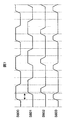
図5は、図1のシステムにおけるタイミングチャートを示す図である。図1のシステムは、クロック信号のデューティ調整回路20を含み構成されている。デューティ調整回路20は調整信号S200に従って動作し、デューティ比をd/(3d+r+s)となるように調整した信号をクロック信号S107として出力する。ここで記号dは図4と同様にノード間の信号伝送時間を表す。図5の最初の一周期は読み出し動作を表し、メモリアドレスA1からデータRDを読み出す。ここではメモリ側で受信するクロック信号S111の立下りエッジから、時間rだけ経過後に読み出しデータ信号S116が確定するものとする。すなわち、時間rはメモリにおけるデータ信号の入力から出力に至るまでの処理時間である。また、記号sはCPU側のデータ信号のセットアップ時間を示す。この結果、タイミングチャートは図示のようになり、レイテンシの下限L1と動作周波数の上限F1は以下のようになる。
L1=3d+r+s、F1=1/L1
例えばd=10ns、r=10ns、s=5nsの場合、図4で説明した従来技術ではF0=14.3MHzであるのに対し、本実施例ではF1=22.2MHzとなる。
【0017】
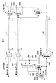
図6は、本発明に用いるデューティ調整回路の一実施例を示すブロック図である。本例のデューティ調整回路20は、デューティ設定用遅延回路60、論理積回路61、および位相調整用遅延回路62を備えて構成される。図7は、図6のデューティ調整回路におけるタイミングチャートである。以下、このタイミングチャートを用いてデューティ調整回路20の動作を説明する。まず、デューティ設定用遅延回路60は調整信号S200に従い、クロック信号S600のデューティ比がd/(3d+r+s)となるように、遅延された信号S601を出力する。論理積回路61は、信号S600と信号S601の論理積を信号S602として出力する。ここで、信号S602と信号S600とでは位相がずれているため、位相調整用遅延回路62は両信号の立上りエッジが同期するように遅延を設定し、クロック出力として信号S603を出力する。
【0018】
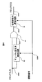
図8は、デューティ調整回路に入力される調整信号の生成方法の一例を示すブロック図である。図示のように、第1のノードであるCPU側には、伝送路30に対して設けられたデューティ調整回路20と、調整起動信号を入力し調整信号を出力する第1の制御部80と、伝送路34、35に対してそれぞれ設けられたマルチプレクサ(MUX)81およびデマルチプレクサ(DMUX)82と、位相差を検出する位相差検出回路83と、記憶装置であるROM84とが備えられている。また、第2のノードであるメモリ側には、伝送路34を介して信号を入力する第1の制御部90と、伝送路35、34に対してそれぞれ設けられたマルチプレクサ(MUX)91およびデマルチプレクサ(DMUX)92とが備えられている。
【0019】
以下、図8を参照しながらデューティ調整信号S200の生成方法について説明する。まず、デューティ調整信号S200の算出に必要となる信号伝送時間d、メモリの読み出し時間r、CPUのセットアップ時間sのうち、メモリの読み出し時間rとCPUのセットアップ時間sはシステム固有の値であるため、予め算出し信号S807によりROM84に格納する。信号伝送時間dは伝送路の長さ等で変動するため、これを次のようにして算出する。第1の制御部80は、調整起動信号S800により起動され、信号S804によりマルチプレクサ81とデマルチプレクサ82に選択を指示し、各々信号S801と信号S802を選択する。そして、信号S801を伝送路34を介して伝送し、メモリ側に設けられた第2の制御部90に対して調整起動を指示する。第2の制御部90は調整起動を受けて、信号S810によりマルチプレクサ91とデマルチプレクサ92に選択を指示し、いずれも信号S811を選択する。なお、図中、信号S805、S815は書き込みデータ信号、信号S806、S816は読み込みデータ信号である。
【0020】
次に、第1の制御部80は信号S801としてテスト信号を出力する。テスト信号はマルチプレクサ81および伝送路34を介してメモリ側へ伝送され、デマルチプレクサ92、マルチプレクサ91、および伝送路35を介してCPU側へと戻る。位相差検出回路83は、元のテスト信号である信号S801と、戻された信号S802の位相差(時間差)を検出し、その検出結果を信号S803として第1の制御部80に出力する。信号S803はCPU側とメモリ側の往復に要する伝送時間に相当し、この半分の値を上記の信号伝送時間dとする。第1の制御部80は、この算出された信号伝送時間dおよび予め算出されたメモリの読み出し時間rとCPUのセットアップ時間sの値に基づいて、調整信号S200を生成し、デューティ調整回路20に出力する。
【0021】
本例はCPUとメモリが1対1で設けられている場合であるが、複数のCPUと複数のメモリを有するシステムの場合は、この調整信号は、各CPUから各メモリへの信号伝送時間の最大値と、各メモリから各CPUへの信号伝送時間の最大値と、各メモリにおけるデータ信号の入力から出力に至るまでの処理時間の最大値とに基づいて生成することができる。また、第1の制御部80から出力されるテスト信号は、本システムの電源投入直後および/または伝送路の未使用時間に送信することができる。特にシステムを取り巻く環境、例えば温度や湿度、または電源電圧の変動などが生じたときは、それをセンサ等によって検出し、必要に応じてテスト信号を出力し、クロック信号のデューティ比を変更することが好ましい。
【0022】
ここで、CPUメモリバスは光伝送路で構成することができる。この場合、CPUとメモリに設けられる各出力手段は電気信号を光信号に変換する半導体レーザ等の発光素子を有する電気光変換手段を備える。一方、入力手段は光信号を電気信号に変換する発光ダイオード等の受光素子を有する光電気変換手段を備える。この電気光変換手段と光電気変換手段との間は光伝送路により光学的に接続される。この場合の信号伝送時間は、電気光変換手段における電気光変換時間および光電気変換手段における光電気変換時間を含むものである。
【0023】
以下に関しては本実施例における一つの実現例であり、本発明を制約するものではない。
(1)各信号は正論理であっても負論理であってもよい。(2)図1、図2、図3、図8においては、読み出しデータ信号、書き込みデータ信号、アドレス信号、R/W信号、CS信号、クロック信号が全て異なる伝送路により伝送されているが、全ての信号もしくはこれらのうち一部の信号を同じ伝送路により伝送する方式でもよい。(3)図4、図5においては、メモリの読み出しがメモリの受信クロック信号S111の立下りエッジから開始しているが、例えばCS信号、R/W信号およびアドレス信号が確定してからメモリの読み出しが開始され、読み出しデータが内部で確定後の信号S111の立下りエッジにて信号S116がラッチ出力される方式でもよい。この場合はメモリ読み出し時間をr’、ラッチ出力時間をr”とすると、デューティ比は(d+r’)/(3d+r’+r”+s)となるように調整を行う。このとき、従来方式でのレイテンシはL0’=max(d+r’,2d+r”+s)×2、本発明でのレイテンシはL1’=3d+r’+r”+sとなり、改善がなされる。
【0024】
このように本発明では、CPUにおけるデータ送信、データ受信、メモリアクセスの各所要時間から同期伝送クロックのデューティ比を決めることにより、CPUとメモリの待ち時間が削減され、CPUメモリアクセスにおけるレイテンシ削減と伝送帯域の向上を同時に実現することができる。よってシステム全体の性能向上を図ることができる。
【0025】
【発明の効果】
本発明によれば、データ転送におけるレイテンシを低減し、かつ伝送帯域を向上し得る同期伝送システムを提供することができる。
【図面の簡単な説明】
【図1】本発明に係る同期伝送システムの一実施例を示す図である。
【図2】本発明に係る同期伝送システムを用いて構成されるCPUメモリバスの一例を示すブロック図である。
【図3】従来の同期伝送システムの一例を示す図である。
【図4】図3のシステムにおけるタイミングチャートを示す図である。
【図5】図1のシステムにおけるタイミングチャートを示す図である。
【図6】本発明に用いるデューティ調整回路の一実施例を示すブロック図である。
【図7】図6のデューティ調整回路におけるタイミングチャートである。
【図8】デューティ調整回路に入力される調整信号の生成方法の一例を示すブロック図である。
【符号の説明】
20 デューティ調整回路
30〜35 伝送路
S101、S107、S111 クロック信号
S102、S112 CS信号
S103、S113 R/W信号
S104、S114 アドレス信号
S105、S115 書き込みデータ信号
S106、S116 読み出しデータ
S200 調整信号[0001]
BACKGROUND OF THE INVENTION
The present invention relates to a synchronous transmission system for performing signal transmission between a plurality of nodes via a transmission path such as a CPU memory bus that requires high speed and low latency.
[0002]
[Prior art]
Although the operating frequency of the CPU has been improved by the advancement of semiconductor technology, the signal transmission frequency between the CPU memories is an order of magnitude lower than the operating frequency of the CPU, which is a performance bottleneck of the entire CPU memory system. In general, serial transmission is known as a method for improving the bandwidth of a transmission path. This is a method of transmitting a plurality of signals after performing speed conversion by parallel / serial conversion, and performing serial / parallel conversion on the receiving side to obtain the plurality of original signals.
[0003]
However, in the data transfer between the CPU memories, it is necessary not only to improve the bandwidth but also to reduce the data transfer delay time between them, so-called latency. The serial transmission described above has a problem in that in addition to the conventional method, parallel-serial conversion and latency for the time required for serial-parallel conversion increase.
[0004]
FIG. 3 is a diagram illustrating an example of a conventional synchronous transmission system. In this system, one CPU and one memory are connected by
[0005]
FIG. 4 is a diagram showing a timing chart in the system of FIG. As shown in the figure, the signals S102 to S105 output from the CPU are output in synchronization with the rising edge of the clock signal S101 having a duty of 50%. In the R / W signal S103, a value “1” indicates a read and a value “0” indicates a write instruction. The value “0” is valid for the CS signal S102. A symbol d in FIG. 4 represents a signal transmission time between the CPU and the memory. In the following, the signal transmission time d represents the time required for signal transmission from one node to another node, the propagation delay time of the transmission path and circuit parts existing between the nodes, and the synchronization signal generated when passing through the latch circuit Includes all waiting time. However, d in FIG. 4 corresponds to the propagation delay time of the
L0 = max (d, 2d + r + s) × 2 = 4d + 2r + 2s, F0 = 1 / L0
[0006]
Note that Patent Document 1 discloses a clock generation circuit that generates a clock signal having a desired duty based on an input clock signal and a semiconductor memory device that controls operation timing using the clock signal generated by the clock generation circuit. This technique is for avoiding a collision between different operations in the memory, and does not solve the latency problem in the CPU memory bus or the like.
[Patent Document 1]
Japanese Patent Laid-Open No. 2000-99194
[Problems to be solved by the invention]
Accordingly, an object of the present invention is to provide a synchronous transmission system capable of reducing latency in data transfer and improving a transmission band.
[0008]
[Means for Solving the Problems]
The object is to provide a first node comprising first clock signal output means, data signal input means and / or output means, second clock signal input means, data signal input means and / or output means. A synchronous transmission system for transmitting a signal to and from a second node via a transmission path, wherein the first node and / or the second node is the first clock signal and / or Alternatively, this can be achieved by a synchronous transmission system including a duty adjustment circuit that changes the duty ratio of the second clock signal according to the adjustment signal.
[0009]
Here, the adjustment signal is transmitted from the first node to the second node, from the second node to the first node, and from the second node. It can be generated based on the processing time from the input to the output of the data signal. In addition, the synchronous transmission system can include a plurality of the first nodes and / or a plurality of the second nodes. In this case, the adjustment signal includes the maximum value of the signal transmission time from each first node to each second node and the signal transmission time from each second node to each first node. It can be generated based on the maximum value and the maximum value of the processing time from the input to the output of the data signal in each second node.
[0010]
The first node transmits a test signal to the second node, the second node returns the test signal to the first node, the test signal and the returned test signal, The signal transmission time can be calculated from the time difference. The test signal can be transmitted immediately after the system is turned on and / or during the unused time of the transmission line.
[0011]
Further, the output means includes electro-optical conversion means for converting an electric signal into an optical signal, and the input means includes photoelectric conversion means for converting the optical signal into an electric signal, the electro-optical conversion means and the photoelectric conversion The means can be optically connected by an optical transmission line. The signal transmission time can include an electro-optical conversion time in the electro-optical conversion means and a photoelectric conversion time in the photoelectric conversion means.
With this configuration, it is possible to reduce latency in data transfer and improve the transmission band.
[0012]
DETAILED DESCRIPTION OF THE INVENTION
FIG. 1 is a diagram showing an embodiment of a synchronous transmission system according to the present invention. This embodiment shows an example in which one CPU and one memory are connected by
[0013]
In FIG. 1, the CPU-side clock signal S101 is changed in duty ratio by the
[0014]
FIG. 2 is a block diagram showing an example of a CPU memory bus configured using the synchronous transmission system according to the present invention of FIG. The CPU memory bus includes one
[0015]
The CPU memory bus in FIG. 2 is composed of one CPU and a plurality of memories, but may be composed of a plurality of CPUs and one memory, or a plurality of CPUs and a plurality of memories. In this case, the adjustment signal for adjusting the duty ratio includes the maximum value of the signal transmission time from each CPU to each memory, the maximum value of the signal transmission time from each memory to each CPU, and the data signal in each memory. It can be generated based on the maximum value of processing time from input to output. That is, it is adjusted to the slowest one. A method of generating the adjustment signal will be described later. Further, although not shown, a duty adjustment circuit is provided on the CPU side. The duty adjustment circuit can be provided not on the CPU side but on the memory side, or on both the CPU side and the memory side.
[0016]
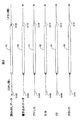
FIG. 5 shows a timing chart in the system of FIG. The system shown in FIG. 1 includes a clock signal
L1 = 3d + r + s, F1 = 1 / L1
For example, in the case of d = 10 ns, r = 10 ns, and s = 5 ns, F0 = 14.3 MHz in the conventional technique described in FIG. 4, whereas F1 = 22.2 MHz in this embodiment.
[0017]
FIG. 6 is a block diagram showing an embodiment of the duty adjustment circuit used in the present invention. The
[0018]
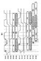
FIG. 8 is a block diagram illustrating an example of a method for generating an adjustment signal input to the duty adjustment circuit. As shown in the figure, on the CPU side which is the first node, a
[0019]
Hereinafter, a method of generating the duty adjustment signal S200 will be described with reference to FIG. First, among the signal transmission time d, the memory read time r, and the CPU setup time s required for calculating the duty adjustment signal S200, the memory read time r and the CPU setup time s are values inherent to the system. , Calculated in advance and stored in the
[0020]
Next, the
[0021]
In this example, the CPU and the memory are provided on a one-to-one basis. However, in the case of a system having a plurality of CPUs and a plurality of memories, this adjustment signal is a signal transmission time from each CPU to each memory. It can be generated based on the maximum value, the maximum value of the signal transmission time from each memory to each CPU, and the maximum value of the processing time from the input to the output of the data signal in each memory. Further, the test signal output from the
[0022]
Here, the CPU memory bus can be composed of an optical transmission path. In this case, each output means provided in the CPU and the memory includes an electro-optical conversion means having a light emitting element such as a semiconductor laser for converting an electric signal into an optical signal. On the other hand, the input means includes photoelectric conversion means having a light receiving element such as a light emitting diode for converting an optical signal into an electric signal. The electro-optical conversion means and the photoelectric conversion means are optically connected by an optical transmission path. The signal transmission time in this case includes the electro-optical conversion time in the electro-optical conversion means and the photoelectric conversion time in the photoelectric conversion means.
[0023]
The following is one implementation example in the present embodiment and does not limit the present invention.
(1) Each signal may be positive logic or negative logic. (2) In FIGS. 1, 2, 3, and 8, the read data signal, the write data signal, the address signal, the R / W signal, the CS signal, and the clock signal are all transmitted through different transmission paths. A method may be used in which all signals or some of these signals are transmitted through the same transmission path. (3) In FIGS. 4 and 5, the memory read-out starts from the falling edge of the memory reception clock signal S111. For example, after the CS signal, the R / W signal and the address signal are determined, Alternatively, the signal S116 may be latched and output at the falling edge of the signal S111 after the reading is started and the read data is internally determined. In this case, when the memory read time is r ′ and the latch output time is r ″, the duty ratio is adjusted to be (d + r ′) / (3d + r ′ + r ″ + s). At this time, the latency in the conventional method is L0 ′ = max (d + r ′, 2d + r ″ + s) × 2, and the latency in the present invention is L1 ′ = 3d + r ′ + r ″ + s, which is improved.
[0024]
As described above, in the present invention, by determining the duty ratio of the synchronous transmission clock from the time required for data transmission, data reception, and memory access in the CPU, the waiting time between the CPU and the memory is reduced, and latency in the CPU memory access is reduced. Improvement of the transmission band can be realized at the same time. Therefore, the performance of the entire system can be improved.
[0025]
【The invention's effect】
ADVANTAGE OF THE INVENTION According to this invention, the synchronous transmission system which can reduce the latency in data transfer and can improve a transmission band can be provided.
[Brief description of the drawings]
FIG. 1 is a diagram showing an embodiment of a synchronous transmission system according to the present invention.
FIG. 2 is a block diagram showing an example of a CPU memory bus configured using the synchronous transmission system according to the present invention.
FIG. 3 is a diagram illustrating an example of a conventional synchronous transmission system.
FIG. 4 is a diagram showing a timing chart in the system of FIG. 3;
FIG. 5 is a diagram showing a timing chart in the system of FIG. 1;
FIG. 6 is a block diagram showing an embodiment of a duty adjustment circuit used in the present invention.
7 is a timing chart in the duty adjustment circuit of FIG. 6;
FIG. 8 is a block diagram illustrating an example of a method for generating an adjustment signal input to a duty adjustment circuit.
[Explanation of symbols]
20
Claims (8)
Priority Applications (1)
| Application Number | Priority Date | Filing Date | Title |
|---|---|---|---|
| JP2003069938A JP4158564B2 (en) | 2003-03-14 | 2003-03-14 | Synchronous transmission system |
Applications Claiming Priority (1)
| Application Number | Priority Date | Filing Date | Title |
|---|---|---|---|
| JP2003069938A JP4158564B2 (en) | 2003-03-14 | 2003-03-14 | Synchronous transmission system |
Publications (2)
| Publication Number | Publication Date |
|---|---|
| JP2004282330A JP2004282330A (en) | 2004-10-07 |
| JP4158564B2 true JP4158564B2 (en) | 2008-10-01 |
Family
ID=33286813
Family Applications (1)
| Application Number | Title | Priority Date | Filing Date |
|---|---|---|---|
| JP2003069938A Expired - Fee Related JP4158564B2 (en) | 2003-03-14 | 2003-03-14 | Synchronous transmission system |
Country Status (1)
| Country | Link |
|---|---|
| JP (1) | JP4158564B2 (en) |
Cited By (1)
| Publication number | Priority date | Publication date | Assignee | Title |
|---|---|---|---|---|
| US10951198B1 (en) | 2019-09-18 | 2021-03-16 | Kioxia Corporation | Semiconductor integrated circuit, transmission device, and memory device |
Families Citing this family (6)
| Publication number | Priority date | Publication date | Assignee | Title |
|---|---|---|---|---|
| JP4656221B2 (en) | 2008-09-30 | 2011-03-23 | 株式会社デンソー | Communication apparatus and clock synchronous communication system |
| JP2018167466A (en) * | 2017-03-29 | 2018-11-01 | ブラザー工業株式会社 | COMMUNICATION DEVICE AND RECORDING DEVICE HAVING THE SAME |
| CN115723430A (en) | 2019-02-06 | 2023-03-03 | 惠普发展公司,有限责任合伙企业 | Printed parts and methods of manipulating printed parts |
| PL4206896T3 (en) | 2019-02-06 | 2024-10-28 | Hewlett-Packard Development Company L.P. | Identifying random bits in control data packets |
| WO2020162894A1 (en) * | 2019-02-06 | 2020-08-13 | Hewlett-Packard Development Company, L.P. | Data packets comprising random numbers for controlling fluid dispensing devices |
| EP3717254B1 (en) | 2019-02-06 | 2023-12-20 | Hewlett-Packard Development Company, L.P. | Integrated circuit with address drivers for fluidic die |
-
2003
- 2003-03-14 JP JP2003069938A patent/JP4158564B2/en not_active Expired - Fee Related
Cited By (1)
| Publication number | Priority date | Publication date | Assignee | Title |
|---|---|---|---|---|
| US10951198B1 (en) | 2019-09-18 | 2021-03-16 | Kioxia Corporation | Semiconductor integrated circuit, transmission device, and memory device |
Also Published As
| Publication number | Publication date |
|---|---|
| JP2004282330A (en) | 2004-10-07 |
Similar Documents
| Publication | Publication Date | Title |
|---|---|---|
| JP4040953B2 (en) | Data input circuit and data input method for synchronous semiconductor memory device | |
| KR100535649B1 (en) | DQS generating circuit in a DDR memory device and method of generating the DQS | |
| TW201140091A (en) | System and device for reducing instantaneous voltage droop during a scan shift operation | |
| JP2003281888A (en) | Output control signal generation circuit and output control signal generation method for synchronous semiconductor memory device | |
| KR20090061515A (en) | Connection circuit for BALS system and its operation method | |
| JPH1139869A (en) | Semiconductor device system and semiconductor device | |
| JP4158564B2 (en) | Synchronous transmission system | |
| JP2011175619A (en) | Timing adjusting method between internal clock and command, semiconductor memory device, and memory system | |
| US20150098296A1 (en) | Semiconductor device and semiconductor system with the same | |
| JP3560793B2 (en) | Data transfer method | |
| WO2004061860A1 (en) | Semiconductor memory device and method for controlling semiconductor memory device | |
| JP3648070B2 (en) | Operation control circuit and operation control method for integrated circuit memory device | |
| KR101188264B1 (en) | Semiconductor System, Semiconductor Memory Apparatus, and Method for Input/Output of Data Using the Same | |
| KR980005013A (en) | Synchronous semiconductor memory circuit | |
| JP4387371B2 (en) | Memory device, its use, and data word synchronization method | |
| JP2004282723A (en) | Clock generation circuit, semiconductor integrated circuit device, and clock generation method | |
| US20110064087A1 (en) | Method for Dynamical Adjusting Channel Direction and Network-on-Chip Architecture thereof | |
| US6226222B1 (en) | Synchronous semiconductor memory device having a function for controlling sense amplifiers | |
| US10504569B2 (en) | System and method for controlling phase alignment of clock signals | |
| US7154809B2 (en) | Method for measuring the delay time of a signal line | |
| US7705651B2 (en) | Delay circuit of semiconductor memory apparatus | |
| KR20140126145A (en) | Semiconductor device, semiconductor system with the semiconductor device and method of driving the semiconductor system | |
| JP4248074B2 (en) | System having an operation timing control function | |
| KR100728556B1 (en) | Data output circuit of semiconductor memory device | |
| KR100498415B1 (en) | Clock generation circuit and synchronous semiconductor device having the same |
Legal Events
| Date | Code | Title | Description |
|---|---|---|---|
| A621 | Written request for application examination |
Free format text: JAPANESE INTERMEDIATE CODE: A621 Effective date: 20060221 |
|
| A977 | Report on retrieval |
Free format text: JAPANESE INTERMEDIATE CODE: A971007 Effective date: 20070830 |
|
| TRDD | Decision of grant or rejection written | ||
| A01 | Written decision to grant a patent or to grant a registration (utility model) |
Free format text: JAPANESE INTERMEDIATE CODE: A01 Effective date: 20080624 |
|
| A01 | Written decision to grant a patent or to grant a registration (utility model) |
Free format text: JAPANESE INTERMEDIATE CODE: A01 |
|
| A61 | First payment of annual fees (during grant procedure) |
Free format text: JAPANESE INTERMEDIATE CODE: A61 Effective date: 20080707 |
|
| R150 | Certificate of patent or registration of utility model |
Free format text: JAPANESE INTERMEDIATE CODE: R150 |
|
| FPAY | Renewal fee payment (event date is renewal date of database) |
Free format text: PAYMENT UNTIL: 20110725 Year of fee payment: 3 |
|
| FPAY | Renewal fee payment (event date is renewal date of database) |
Free format text: PAYMENT UNTIL: 20110725 Year of fee payment: 3 |
|
| FPAY | Renewal fee payment (event date is renewal date of database) |
Free format text: PAYMENT UNTIL: 20120725 Year of fee payment: 4 |
|
| FPAY | Renewal fee payment (event date is renewal date of database) |
Free format text: PAYMENT UNTIL: 20130725 Year of fee payment: 5 |
|
| LAPS | Cancellation because of no payment of annual fees |