JP4149404B2 - Evaluation chip - Google Patents
Evaluation chip Download PDFInfo
- Publication number
- JP4149404B2 JP4149404B2 JP2004093053A JP2004093053A JP4149404B2 JP 4149404 B2 JP4149404 B2 JP 4149404B2 JP 2004093053 A JP2004093053 A JP 2004093053A JP 2004093053 A JP2004093053 A JP 2004093053A JP 4149404 B2 JP4149404 B2 JP 4149404B2
- Authority
- JP
- Japan
- Prior art keywords
- interrupt
- priority
- signals
- signal
- control
- Prior art date
- Legal status (The legal status is an assumption and is not a legal conclusion. Google has not performed a legal analysis and makes no representation as to the accuracy of the status listed.)
- Expired - Fee Related
Links
- 238000011156 evaluation Methods 0.000 title claims description 7
- 230000007274 generation of a signal involved in cell-cell signaling Effects 0.000 claims description 8
- 238000012545 processing Methods 0.000 claims description 7
- 238000010586 diagram Methods 0.000 description 6
- 230000000694 effects Effects 0.000 description 5
- 230000001360 synchronised effect Effects 0.000 description 5
- 238000000034 method Methods 0.000 description 3
- 238000012986 modification Methods 0.000 description 2
- 230000004048 modification Effects 0.000 description 2
- 230000005540 biological transmission Effects 0.000 description 1
- 230000006870 function Effects 0.000 description 1
- 238000012546 transfer Methods 0.000 description 1
Images


Classifications
-
- G—PHYSICS
- G06—COMPUTING; CALCULATING OR COUNTING
- G06F—ELECTRIC DIGITAL DATA PROCESSING
- G06F13/00—Interconnection of, or transfer of information or other signals between, memories, input/output devices or central processing units
- G06F13/14—Handling requests for interconnection or transfer
- G06F13/20—Handling requests for interconnection or transfer for access to input/output bus
- G06F13/24—Handling requests for interconnection or transfer for access to input/output bus using interrupt
- G06F13/26—Handling requests for interconnection or transfer for access to input/output bus using interrupt with priority control
Description
本発明は、エミュレータ(emulator)に用いるマイクロコンピュータ(以下「マイコン」という。)等のプラグラム開発用集積回路であるエバリュエーションチップ(evaluation chip、以下「EVAチップ」という。)、特に命令実行の割り込み優先順位を任意に変更できるEVAチップに関するものである。 The present invention relates to an evaluation chip (hereinafter referred to as “EVA chip”), which is an integrated circuit for program development such as a microcomputer (hereinafter referred to as “microcomputer”) used in an emulator, particularly an instruction execution interrupt. The present invention relates to an EVA chip whose priority can be arbitrarily changed.
従来、EVAチップに関する技術としては、例えば、次のような文献に記載されるものがあった。 Conventionally, as a technology related to the EVA chip, for example, there are those described in the following documents.
この特許文献1に記載されたEVAチップは、外部のプログラムメモリに格納されたプログラムの評価を行うものであり、中央処理装置(以下「CPU」という。)部、及びデータラッチ部等を内蔵している。この種のEVAチップでは、CPU部により、プログラムメモリから取り込まれた命令がデコードされてこのデコード結果が実行される。この命令実行結果は、データラッチ部で一時保持された後、選択的に外部に出力される。このデータに対し、外部に設けられたトレース回路等によって評価が行われる。 The EVA chip described in Patent Document 1 evaluates a program stored in an external program memory, and includes a central processing unit (hereinafter referred to as “CPU”) unit, a data latch unit, and the like. ing. In this type of EVA chip, the CPU fetches the instruction fetched from the program memory and executes the decoding result. The instruction execution result is temporarily held in the data latch unit and then selectively output to the outside. This data is evaluated by a trace circuit or the like provided outside.
このような特許文献1に記載されたEVAチップにおいて、プログラムメモリに格納されたプログラムに対し、外部から与えられる複数の割り込み要求信号により割り込み処理を行う場合、チップ内に割り込み回路が設けられる。この割り込み回路では、複数の割り込み要求信号が外部から与えられると、予め設定された割り込みの優先順位に従い、複数の割り込み信号を生成し、これらをエンコード(コード化)して割り込みベクタアドレスを生成し、この割り込みベクタアドレスによりCPU部で割り込み処理を行わせる。ここで、割り込みの優先順位が予め設定されているのは、割り込みの優先順位が仕様で決められているので、優先順位を固定することにより、割り込み回路の構成を簡単にできるからである。 In such an EVA chip described in Patent Document 1, an interrupt circuit is provided in the chip when interrupt processing is performed on a program stored in a program memory by a plurality of external interrupt request signals. In this interrupt circuit, when a plurality of interrupt request signals are given from the outside, a plurality of interrupt signals are generated in accordance with preset interrupt priorities, and these are encoded (coded) to generate an interrupt vector address. Then, the interrupt processing is performed in the CPU unit by this interrupt vector address. Here, the reason why the priority order of interrupts is set in advance is that the priority order of interrupts is determined by the specification, so that the configuration of the interrupt circuit can be simplified by fixing the priority order.
しかしながら、従来の割り込み回路を内蔵したEVAチップでは、内部のCPU部の割り込み部分で、優先順位の仕様変更が発生した場合、又は、CPU部のシリーズ品において、割り込み部分で優先順位の仕様が異なる場合、用意されているEVAチップは、搭載されている割り込み回路の優先順位が固定されているため、EVAチップが使用できなくなり、不利不便であった。 However, in the EVA chip incorporating the conventional interrupt circuit, when the priority specification is changed in the interrupt portion of the internal CPU unit, or in the series part of the CPU unit, the priority specification is different in the interrupt portion. In this case, since the priority order of the installed EVA circuit is fixed, the EVA chip cannot be used, which is disadvantageous.
前記課題を解決するために、本発明のEVAチップは、割り込み変更信号を出力する複数の割り込み優先順位決定回路と、割り込み信号を出力する複数の割り込み信号生成回路と、割り込みベクタアドレス生成回路と、命令実行手段とを備え、外部から与えられる複数の割り込み要求信号に基づき、対応する割り込み処理を順に実行するEVAチップにおいて、次のような構成にしている。 In order to solve the above problems, an EVA chip of the present invention includes a plurality of interrupt priority determination circuits that output an interrupt change signal, a plurality of interrupt signal generation circuits that output an interrupt signal, an interrupt vector address generation circuit, An EVA chip that includes instruction execution means and sequentially executes corresponding interrupt processing based on a plurality of interrupt request signals given from outside has the following configuration.
前記割り込み優先順位決定回路は、対応する前記割り込み信号生成回路以外が生成した複数の前記割り込み信号と、外部から与えられる割り込み優先順位変更制御用の複数の制御信号との論理を求めて、前記割り込み変更信号を出力する回路である。前記割り込み信号生成回路は、対応する前記割り込み優先順位決定回路が出力する前記割り込み変更信号と、対応する前記割り込み要求信号との論理を求めて、前記複数の割り込み要求信号の全てが発生しているときに、前記複数の制御信号で設定される優先順位に従って、前記割り込み信号を順に生成する回路である。前記割り込みベクタアドレス生成回路は、複数の前記割り込み信号をエンコードして割り込みベクタアドレスを生成する回路である。更に、前記命令実行手段は、前記割り込みベクタアドレスに基づき、外部から優先順に取り込んだ割り込み命令をデコードしてこのデコード結果を順に実行するものである。The interrupt priority determination circuit obtains logic of a plurality of interrupt signals generated by other than the corresponding interrupt signal generation circuit and a plurality of control signals for interrupt priority change control given from the outside, and This circuit outputs a change signal. The interrupt signal generation circuit obtains the logic of the interrupt change signal output from the corresponding interrupt priority determination circuit and the corresponding interrupt request signal, and all of the plurality of interrupt request signals are generated. Sometimes, the interrupt signal is generated in order according to the priority set by the plurality of control signals. The interrupt vector address generation circuit is a circuit that encodes a plurality of the interrupt signals to generate an interrupt vector address. Further, the instruction execution means decodes interrupt instructions fetched from the outside in order of priority based on the interrupt vector address, and sequentially executes the decoded results.
本発明のEVAチップによれば、外部から与えられる割り込み優先順位変更制御用の複数の制御信号により、各割り込み信号生成回路の割り込み優先順位を任意に変更可能な構成にしたので、複数の割り込み信号生成回路の優先順位が異なる命令実行手段に対して、1種類のEVAチップで対応可能となり、使い勝手が良く、コストを削減できる。 According to the EVA chip of the present invention, the interrupt priority order of each interrupt signal generation circuit can be arbitrarily changed by a plurality of control signals for interrupt priority order change control given from the outside. Instruction execution means having different generation circuit priorities can be handled by one type of EVA chip, which is easy to use and can reduce costs.
複数の制御信号を、複数の優先順位制御レジスタにより生成する構成にすると、割り込み数が増加しても制御信号入力端子数が増加しないので、端子ネックを解消できる。 When a plurality of control signals are generated by a plurality of priority control registers, the number of control signal input terminals does not increase even if the number of interrupts increases, so that a terminal neck can be eliminated.
複数の制御信号を、割り込み優先順位制御シフトレジスタにより生成する構成にすると、EVAチップを制御するCPU等に頼らないスタンドアローン方式の動作が可能となる。 When a plurality of control signals are generated by the interrupt priority control shift register, a stand-alone operation that does not depend on the CPU or the like that controls the EVA chip is possible.
本発明のEVAチップでは、外部から与えられる割り込み優先順位変更制御用の複数の制御信号と、複数の割り込み信号との論理をそれぞれ求めて、割り込み変更信号をそれぞれ出力する複数の割り込み優先順位決定回路と、前記複数の割り込み変更信号と、外部から与えられる複数の割り込み要求信号との論理を求めて、前記各割り込み信号をそれぞれ出力する複数の割り込み信号生成回路と、前記複数の割り込み信号をエンコードして割り込みベクタアドレスを生成する割り込みベクタアドレス生成回路と、前記割り込みベクタアドレスに基づき、外部から優先順に取り込んだ割り込み命令をデコードしてこのデコード結果を順に実行するマイコンコアで構成された命令実行手段とを備えている。 In the EVA chip of the present invention, a plurality of interrupt priority determination circuits for obtaining the logic of a plurality of control signals for interrupt priority change control and a plurality of interrupt signals given from the outside and outputting the interrupt change signals respectively. And calculating the logic of the plurality of interrupt change signals and a plurality of interrupt request signals given from the outside, and encoding a plurality of interrupt signals, and a plurality of interrupt signal generation circuits for outputting the respective interrupt signals, respectively. An interrupt vector address generation circuit for generating an interrupt vector address, and an instruction execution means configured by a microcomputer core for decoding interrupt instructions fetched from the outside in priority order based on the interrupt vector address and sequentially executing the decoded results; It has.
ここで、前記複数の制御信号は、外部の制御信号入力端子から入力される構成、或いは、外部から与えられるデータに基づき、内部に設けた複数の優先順位制御レジスタにより生成する構成にしている。又、前記複数の制御信号は、外部から与えられるシリアルデータに基づき、内部に設けた割り込み優先順位制御シフトレジスタにより、パワーオン時に生成する構成にしても良い。 Here, the plurality of control signals are configured to be input from an external control signal input terminal, or to be generated by a plurality of priority order control registers provided inside based on data supplied from the outside. The plurality of control signals may be generated at power-on by an interrupt priority control shift register provided inside based on serial data given from the outside.
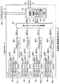
(構成)
図1は、本発明の実施例1を示すEVAチップの概略の構成図である。
(Constitution)
FIG. 1 is a schematic configuration diagram of an EVA chip showing Embodiment 1 of the present invention.
このEVAチップ10は、外部のプログラムメモリ100に格納されたプログラムの評価を行うものであり、そのプログラムに対する割り込み優先順位変更制御用の複数(例えば、4つ)の各4ビット制御信号S11,S12,S13,S14を入力する4組の制御信号入力端子11−1〜11−4,12−1〜12−4,13−1〜13−4,14−1〜14−4と、4つの割り込み要求信号を入力する4つの割り込み要求信号入力端子15−1〜15−4と、プログラムメモリ100から取り込んだ命令を入力する命令入力端子16と、その命令を取り込むためのアドレスを出力するアドレス出力端子17と、複数のデータ出力端子18と、複数の制御信号を出力する複数の制御信号出力端子19とを有している。
The EVA
各制御信号S11,S12,S13,S14は、例えば,4ビットのディジタル信号でそれぞれ構成され、これらを入力するための4組の制御信号入力端子11−1〜11−4,12−1〜12−4,13−1〜13−4,14−1〜14−4に、4つの割り込み優先順位決定回路20−1〜20−4がそれぞれ接続されている。各割り込み優先順位決定回路20−1〜20−4は、外部から入力される各制御信号S11〜S14と、チップ内部から与えられる4つの割り込み信号S31−1〜S31−4の内の3つの割り込み信号との論理をそれぞれ求めて、割り込み変更信号S24−1〜S24−4をそれぞれ出力する回路である。 Each of the control signals S11, S12, S13, and S14 is composed of, for example, a 4-bit digital signal, and four sets of control signal input terminals 11-1 to 11-4 and 12-1 to 12 for inputting these signals. Four interrupt priority determination circuits 20-1 to 20-4 are connected to -4, 13-1 to 13-4, and 14-1 to 14-4, respectively. Each of the interrupt priority determination circuits 20-1 to 20-4 has three interrupts among the control signals S11 to S14 inputted from the outside and four interrupt signals S31-1 to S31-4 given from the inside of the chip. This circuit obtains the logic of each signal and outputs interrupt change signals S24-1 to S24-4.
割り込み優先順位決定回路20−1は、入力端子11−2〜11−4と割り込み信号S31−2〜S31−4線とに接続された3つの2入力ANDゲート21−1,22−1,23−1と、これらのANDゲート21−1〜23−11の出力端子と入力端子11−1とに接続された1つの4入力ORゲート24−1とで構成され、このORゲート24−1から割り込み変更信号S24−1が出力される。同様に、他の各割り込み優先順位決定回路20−2〜20−4も、各3つの2入力ANDゲート21−2〜23−2,21−3〜23−3,21−4〜23−4と、各1つの4入力ORゲート24−2〜24−4とで構成され、この各ORゲート24−2〜24−4から各割り込み変更信号S24−2〜24−4がそれぞれ出力される。これらの各割り込み変更信号S24−1〜S24−4線には、4つの割り込み信号生成回路(例えば、割り込みモジュール)30−1〜30−4がそれぞれ接続されている。 The interrupt priority determination circuit 20-1 includes three 2-input AND gates 21-1, 22-1 and 23 connected to the input terminals 11-2 to 11-4 and the interrupt signals S31-2 to S31-4. -1 and one 4-input OR gate 24-1 connected to the output terminals of these AND gates 21-1 to 23-11 and the input terminal 11-1, and the OR gate 24-1 An interrupt change signal S24-1 is output. Similarly, each of the other interrupt priority determination circuits 20-2 to 20-4 also includes three two-input AND gates 21-2 to 23-2, 21-3 to 23-3, and 21-4 to 23-4. And four one-input OR gates 24-2 to 24-4, and the interrupt change signals S24-2 to 24-4 are output from the OR gates 24-2 to 24-4, respectively. Four interrupt signal generation circuits (for example, interrupt modules) 30-1 to 30-4 are connected to the respective interrupt change signals S24-1 to S24-4.
各割り込みモジュール30−1〜30−4は、各割り込み変更信号S24−1〜S24−4と、外部から入力される各割り込み要求信号S15−1〜S15−4との論理(例えば、AND論理)を求めて、各割り込み信号S31−1〜S31−4をそれぞれ出力する回路であり、例えば、各1つの2入力ANDゲート31−1〜31−4により構成されている。割り込み信号S31−1〜S31−4線は、ANDゲート21−1〜23−1,21−2〜23−2,21−3〜23−3,21−4〜23−4の入力端子に接続されると共に、割り込みベクタアドレス生成回路40に接続されている。割り込みベクタアドレス生成回路40は、4つの割り込み信号S31−1〜S31−4をエンコードして割り込みベクタアドレスS40を生成する回路であり、例えば、エンコーダ組み合わせ回路等で構成されている。この割り込みベクタアドレス生成回路40の出力端子には、命令実行手段(例えば、CPUで構成された対象マイコンのコア、これを以下単に「マイコンコア」という。)50が接続されている。
Each of the interrupt modules 30-1 to 30-4 has logic (for example, AND logic) between the interrupt change signals S24-1 to S24-4 and the interrupt request signals S15-1 to S15-4 input from the outside. And outputs each of the interrupt signals S31-1 to S31-4, and is constituted by, for example, one two-input AND gates 31-1 to 31-4. The interrupt signals S31-1 to S31-4 are connected to input terminals of AND gates 21-1 to 23-1, 212-2 to 23-2, 21-3 to 23-3, and 21-4 to 23-4. At the same time, it is connected to the interrupt vector
マイコンコア50は、割り込みベクタアドレスS40に基づき、プログラムメモリ100から優先順に取り込んだ割り込み命令(割り込みプログラム)をデコードしてこのデコード結果を順に実行するものであり、これには命令入力端子16、アドレス出力端子17、複数のデータ出力端子18、及び複数の制御信号出力端子19が接続されている。このマイコンコア50は、例えば、命令入力端子16から取り込んだプログラムメモリ100内の割り込みプログラムを命令レジスタで保持し、その割り込みプログラムを命令デコーダで解読して各種の制御信号を出力する制御部51と、算術論理ユニット(以下「ALU」という。)52−1でデータの算術演算と論理演算を行い、そのデータを累算器であるアキュムレータ(以下「ACC」という。)52−2で一時記憶する演算部52と、プロクラムメモリ100に対するリードアドレスを指定するプログラムカウンタや各種のレジスタを有するレジスタ部53と、データの記憶を行う随時読み書き可能なメモリ(以下「RAM」という。)54とを備えている。
The
このマイコンコア50からは、例えば、ACC52−2へのライトデータ、RAM54のライトデータ、及びRAM54に対するライトアドレスが出力され、データバスを介して複数のデータ出力端子18から外部へ出力される。更に、マイコンコア50内の制御部51から、ACC52−2のライトデータのラッチタイミングを示すACCデータラッチ信号、RAM54へのライトデータのラッチタイミングを示すRAMデータラッチ信号、及びRAMアドレスのラッチタイミングを示すRAMアドレスラッチ信号等が出力され、複数の信号線を介して複数の制御信号出力端子19から外部へ出力される。
From the
(動作)
EVAチップ10を用いてプログラムメモリ100内のプログラムの評価を行う場合、マイコンコア50内のレジスタ部53からライトアドレスを出力し、このライトアドレスを出力端子17を介してプログラムメモリ100へ与え、そのライトアドレスに対応する命令を読み出す。読み出された命令は、入力端子16を介してマイコンコア50内の制御部51へ送られる。制御部51では、プログラムメモリ100からの命令を命令レジスタに一時記憶し、この記憶した命令を命令デコーダでデコードしてマイコンコア50内を制御する各種の制御信号を出力すると共に、ACCデータラッチ信号、RAMデータラッチ信号、及びRAMアドレスラッチ信号等を出力して複数の出力端子19から外部へ送出する。マイコンコア50内では、演算部52内のALU52−1及びACC52−2等を用いて演算を行い、プログラムメモリ100からの命令を実行してこの命令実行結果をRAM54等に格納し、複数の出力端子18から外部へ送出する。
(Operation)
When evaluating the program in the
出力端子18及び19に接続された外部の図示しない装置では、例えば、ACCデータラッチ信号に基づき、ACCデータをラッチし、トレース回路等によってそのACCデータの評価を行う。
In an external device (not shown) connected to the
マイコンコア50は、プラグラムメモリ100内の命令の実行中に、外部からの割り込み要求信号S15−1〜S15−4に基づき、割り込みベクタアドレス生成回路40から、第1優先順位の割り込みベクタアドレスS40が与えられると、現在の命令実行を中断し、その割り込みベクタアドレスS40で指定されるプログラムメモリ100内の割り込みプログラムを実行する。割り込みプログラムの実行が終了すると、中断していた命令の実行を再開する。
During execution of the instruction in the
その後、外部からの割り込み要求信号S15−1〜S15−4に基づき、割り込みベクタアドレス生成回路40から、第2、第3、第4優先順位の割り込みベクタアドレスS40が順次与えられると、マイコンコア50によって前記と同様の割り込み処理が行われる。
After that, when the interrupt vector addresses S40 of the second, third, and fourth priorities are sequentially given from the interrupt vector
従来のEVAチップでは、割り込みの優先順位が、割り込み要因を接続する順番で予め決定されているが、本実施例1では、外部から入力端子11−1〜11−4,12−1〜12−4,13−1〜13−4,14−1〜14−4に与える制御信号S11〜S14の電位(例えば、グランドGND電位の論理0又は電源電位VCCの論理1)により、各割り込みモジュール30−1〜30−4の割り込み優先順位を任意に切り替えることができる。 In the conventional EVA chip, the priority order of interrupts is determined in advance in the order in which interrupt factors are connected. In the first embodiment, the input terminals 11-1 to 11-4 and 12-1 to 12- are externally input. 4, 13-1 to 13-4, 14-1 to 14-4 according to the potential of the control signals S 11 to S 14 (for example, logic 0 of the ground GND potential or logic 1 of the power supply potential VCC). The interrupt priority order of 1 to 30-4 can be arbitrarily switched.
例えば、割り込み優先順位を割り込みモジュール30−2、割り込みモジュール30−4、割り込みモジュール30−1、割り込みモジュール30−3の順にするには、各入力端子11−1〜11−4,12−1〜12−4,13−1〜13−4,14−1〜14−4に与える制御信号S11〜S14の電位を次のように設定する。この際、外部から入力端子15−1〜15−4に与える割り込み要求信号S15−1〜S15−4の電位は、全て1にする。
入力端子11−1〜11−4に与える制御信号S11の電位;0,0,0,1
入力端子12−1〜12−4に与える制御信号S12の電位;1,0,0,0
入力端子13−1〜13−4に与える制御信号S13の電位;0,0,1,0
入力端子14−1〜14−4に与える制御信号S14の電位;0,1,0,0
For example, in order of the interrupt priority order of the interrupt module 30-2, the interrupt module 30-4, the interrupt module 30-1, and the interrupt module 30-3, the input terminals 11-1 to 11-4, 12-1 to The potentials of the control signals S11 to S14 given to 12-4, 13-1 to 13-4, and 14-1 to 14-4 are set as follows. At this time, all of the potentials of the interrupt request signals S15-1 to S15-4 given to the input terminals 15-1 to 15-4 from the outside are set to 1.
The potential of the control signal S11 given to the input terminals 11-1 to 11-4; 0, 0, 0, 1
Potential of control signal S12 applied to input terminals 12-1 to 12-4; 1, 0, 0, 0
The potential of the control signal S13 applied to the input terminals 13-1 to 13-4; 0, 0, 1, 0
The potential of the control signal S14 applied to the input terminals 14-1 to 14-4; 0, 1, 0, 0
入力端子12−1の電位が1のため、ORゲート24−2の出力の割り込み変更信号S24−2の電位が1、ANDゲート31−2の出力の割り込み信号S31−2が1となり、割り込みモジュール30−1が第1優先順位となる。割り込み信号S31−2の電位が1のため、ANDゲート21−4の出力電位が1、ORゲート24−4の出力の割り込み変更信号S24−4の電位が1、ANDゲート31−4の出力の割り込み信号S31−4の電位が1となり、割り込みモジュール30−4が第2優先順位となる。 Since the potential of the input terminal 12-1 is 1, the potential of the interrupt change signal S24-2 output from the OR gate 24-2 is 1, the interrupt signal S31-2 output from the AND gate 31-2 is 1, and the interrupt module 30-1 is the first priority. Since the potential of the interrupt signal S31-2 is 1, the output potential of the AND gate 21-4 is 1, the potential of the interrupt change signal S24-4 of the output of the OR gate 24-4 is 1, and the output of the AND gate 31-4 is The potential of the interrupt signal S31-4 becomes 1, and the interrupt module 30-4 has the second priority.
割り込み信号S31−4の電位が1のため、ANDゲート23−1の出力電位が1、ORゲート24−1の出力の割り込み変更信号S24−1の電位が1、ANDゲート31−1の出力の割り込み信号S31−1の電位が1となり、割り込みモジュール30−1が第3優先順位となる。割り込み信号S31−1の電位が1のため、ANDゲート22−3の出力電位が1、ORゲート24−3の出力の割り込み変更信号S24−3の電位が1、ANDゲート31−3の出力の割り込み信号S31−3の電位が1となり、割り込みモジュール30−3が第4優先順位となる。 Since the potential of the interrupt signal S31-4 is 1, the output potential of the AND gate 23-1 is 1, the potential of the interrupt change signal S24-1 of the output of the OR gate 24-1 is 1, and the output of the AND gate 31-1 is The potential of the interrupt signal S31-1 becomes 1, and the interrupt module 30-1 has the third priority. Since the potential of the interrupt signal S31-1 is 1, the output potential of the AND gate 22-3 is 1, the potential of the interrupt change signal S24-3 output from the OR gate 24-3 is 1, and the output of the AND gate 31-3 is The potential of the interrupt signal S31-3 becomes 1, and the interrupt module 30-3 has the fourth priority.
そのため、第1、第2、第3、第4優先順位の割り込み信号S31−2,S31−4,S31−1,S31−3に対応する割り込みベクタアドレスS40が、割り込みベクタアドレス生成回路40から出力され、その優先順位に従ってマイコンコア50が割り込み処理を行う。
Therefore, the interrupt vector address S40 corresponding to the interrupt signals S31-2, S31-4, S31-1, and S31-3 having the first, second, third, and fourth priorities is output from the interrupt vector
(効果)
本実施例1では、外部から入力端子11−1〜11−4,12−1〜12−4,13−1〜13−4,14−1〜14−4に与える制御信号S11〜S14の電位により、各割り込みモジュール30−1〜30−4の割り込み優先順位を任意に変更可能な構成にしたので、割り込みモジュール30−1〜30−4の優先順位が異なるマイコンコア50に対して、1種類のEVAチップ10で対応可能となり、使い勝手が良く、コストを削減できる。
(effect)
In the first embodiment, the potentials of the control signals S11 to S14 given to the input terminals 11-1 to 11-4, 12-1 to 12-4, 13-1 to 13-4, 14-1 to 14-4 from the outside. Therefore, the interrupt priority order of each of the interrupt modules 30-1 to 30-4 can be arbitrarily changed. Therefore, one type is used for the
(構成)
図2は、本発明の実施例2を示すEVAチップの概略の構成図であり、実施例1を示す図1中の要素と共通の要素には共通の符号が付されている。
(Constitution)
FIG. 2 is a schematic configuration diagram of an EVA chip showing Embodiment 2 of the present invention. Elements common to those in FIG. 1 showing Embodiment 1 are denoted by common reference numerals.
実施例1のEVAチップ10では、割り込みモジュール30−1〜30−4における割り込み優先順位の切り替え手段として、制御信号入力端子11−1〜11−4,12−1〜12−4,13−1〜13−4,14−1〜14−4を設けている。これに対し、本実施例2のEVAチップ10Aでは、その制御信号入力端子11−1〜11−4,12−1〜12−4,13−1〜13−4,14−1〜14−4に代えて、4つのデータ入力端子61〜64と、これらにそれぞれ接続された4つの優先順位制御レジスタ71〜74とを設けている。
In the
各データ入力端子61〜64には、EVAチップ10Aを制御するCPU等から、割り込み優先順位に関するデータが入力される。各優先順位制御レジスタ71〜74は、各データ入力端子61〜64から入力されるデータを保持し、図1の割り込み優先順位変更制御用の4ビット制御信号に対応する4ビット信号をそれぞれ出力する回路であり、この回路の出力端子が、図1と同様のANDゲート21−1〜23−1,21−2〜23−2,21−3〜23−3,21−4〜23−4及びORゲート24−1〜24−4に接続されている。その他の構成は、図1の実施例1と同様である。
Data relating to the interrupt priority order is input to the
(動作)
EVAチップ10Aを用いてプログラムメモリ100内のプラグラムの評価を行う場合は、実施例1と同様に動作する。
(Operation)
When the program in the
本実施例2では、EVAチップ10Aを制御するCPU等から与えられるデータを、データ入力端子61〜64を介して優先順位制御レジスタ71〜74に書き込むことで、割り込みモジュール30−1〜30−4における割り込み優先順位を任意に切り替えることができる。
In the second embodiment, data supplied from a CPU or the like that controls the EVA chip 10A is written to the priority order control registers 71 to 74 via the
例えば、割り込み優先順位を割り込みモジュール30−2、割り込みモジュール30−4、割り込みモジュール30−1、割り込みモジュール30−3の順にするには、各優先順位制御レジスタ71〜74の4ビット出力端子の電位が、次のような状態になるように、外部からデータ入力端子61〜64を介して設定する。この際、外部から入力端子15−1〜15−4に与える割り込み要求信号S15−1〜S15−4の電位は、全て論理1にする。
優先順位制御レジスタ71の4ビット出力端子の電位;01H(=0,0,0,1)
優先順位制御レジスタ72の4ビット出力端子の電位;08H(=1,0,0,0)
優先順位制御レジスタ73の4ビット出力端子の電位;02H(=0,0,1,0)
優先順位制御レジスタ74の4ビット出力端子の電位;04H(=0,1,0,0)
For example, to set the interrupt priority in the order of the interrupt module 30-2, the interrupt module 30-4, the interrupt module 30-1, and the interrupt module 30-3, the potentials of the 4-bit output terminals of the priority control registers 71 to 74 are set. Is set from the outside via the
Potential of 4-bit output terminal of
Potential of 4-bit output terminal of
Potential of 4-bit output terminal of
Potential of 4-bit output terminal of
優先順位制御レジスタ72の上から1ビット目の出力端子の電位が1のため、実施例1と同様に、ORゲート24−2の出力の割り込み変更信号S24−2の電位が1、ANDゲート31−2の出力の割り込み信号S31−2が1となり、割り込みモジュール30−1が第1優先順位となる。割り込み信号S31−2の電位が1のため、ANDゲート21−4の出力電位が1、ORゲート24−4の出力の割り込み変更信号S24−4の電位が1、ANDゲート31−4の出力の割り込み信号S31−4の電位が1となり、割り込みモジュール30−4が第2優先順位となる。
Since the potential of the output terminal of the first bit from the top of the
割り込み信号S31−4の電位が1のため、ANDゲート23−1の出力電位が1、ORゲート24−1の出力の割り込み変更信号S24−1の電位が1、ANDゲート31−1の出力の割り込み信号S31−1の電位が1となり、割り込みモジュール30−1が第3優先順位となる。割り込み信号S31−1の電位が1のため、ANDゲート22−3の出力電位が1、ORゲート24−3の出力の割り込み変更信号S24−3の電位が1、ANDゲート31−3の出力の割り込み信号S31−3の電位が1となり、割り込みモジュール30−3が第4優先順位となる。 Since the potential of the interrupt signal S31-4 is 1, the output potential of the AND gate 23-1 is 1, the potential of the interrupt change signal S24-1 of the output of the OR gate 24-1 is 1, and the output of the AND gate 31-1 is The potential of the interrupt signal S31-1 becomes 1, and the interrupt module 30-1 has the third priority. Since the potential of the interrupt signal S31-1 is 1, the output potential of the AND gate 22-3 is 1, the potential of the interrupt change signal S24-3 output from the OR gate 24-3 is 1, and the output of the AND gate 31-3 is The potential of the interrupt signal S31-3 becomes 1, and the interrupt module 30-3 has the fourth priority.
そのため、実施例1と同様に、第1、第2、第3、第4優先順位の割り込み信号S31−2,S31−4,S31−1,S31−3に対応する割り込みベクタアドレスS40が、割り込みベクタアドレス生成回路40から出力され、その優先順位に従ってマイコンコア50が割り込み処理を行う。
Therefore, as in the first embodiment, the interrupt vector address S40 corresponding to the interrupt signals S31-2, S31-4, S31-1, and S31-3 having the first, second, third, and fourth priorities is interrupted. The
(効果)
本実施例2では、次の(1)、(2)のような効果がある。
(effect)
The second embodiment has the following effects (1) and (2).
(1) 本実施例2では、EVAチップ10Aを制御するCPU等から与えられるデータを優先順位制御レジスタ71〜74に書き込むことで、各割り込みモジュール30−1〜30−4の割り込み優先順位を任意に変更可能な構成にしたので、実施例1と同様に、割り込みモジュール30−1〜30−4の優先順位が異なるマイコンコア50に対して、1種類のEVAチップ10Aで対応可能となり、使い勝手が良く、コストを削減できる。
(1) In the second embodiment, the interrupt priority order of each of the interrupt modules 30-1 to 30-4 is arbitrarily set by writing data given from the CPU or the like that controls the EVA chip 10A to the priority order control registers 71 to 74. As in the first embodiment, the
(2) 実施例1では、割り込み数が増加すると、EVAチップ10において制御する制御信号入力端子11−1〜11−4,12−1〜12−4,13−1〜13−4,14−1〜14−4の数も増加し、EVA端子ネックになる虞がある。これに対し、本実施例2では、EVAチップ10A内に優先順位制御レジスタ71〜74を設けることで、端子ネックを解消できる。
(2) In the first embodiment, when the number of interrupts increases, control signal input terminals 11-1 to 11-4, 12-1 to 12-4, 13-1 to 13-4, 14- controlled in the
(構成)
図3は、本発明の実施例3を示すEVAチップの概略の構成図であり、実施例1、2を示す図1、図2中の要素と共通の要素には共通の符号が付されている。
(Constitution)
FIG. 3 is a schematic configuration diagram of an EVA chip showing Embodiment 3 of the present invention. Elements common to those in FIGS. 1 and 2 showing Embodiments 1 and 2 are denoted by common reference numerals. Yes.
実施例2のEVAチップ10Aでは、割り込みモジュール30−1〜30−4における割り込み優先順位の切り替え手段として、データ入力端子61〜64及び優先順位制御レジスタ71〜74を設けている。これに対し、本実施例3のEVAチップ10Bでは、そのデータ入力端子61〜64及び優先順位制御レジスタ71〜74に代えて、3つの入力端子81〜83と、これらに接続された12ビットの割り込み優先順位制御シフトレジスタ90とを設けている。
In the EVA chip 10A of the second embodiment,
入力端子81は、外部から優先順位シリアル12ビットデータS81を入力する端子、入力端子82は、外部から同期クロックS82を入力する端子、及び、入力端子83は、外部からクロックイネーブル信号S83を入力する端子である。12ビットの割り込み優先順位制御シフトレジスタ90は、外部から与えられる同期クロックS82に基づき、外部から与えられるシリアル12ビットデータS81を取り込んでパラレルデータに変換し、図1の割り込み優先順位変更制御用の4ビット制御信号×4に対応する16ビット信号をパラレルに出力する回路であり、この回路の16個の出力端子が、図1と同様のANDゲート21−1〜23−1,21−2〜23−2,21−3〜23−3,21−4〜23−4及びORゲート24−1〜24−4に接続されている。その他の構成は、図1、図2の実施例1、2と同様である。
The input terminal 81 is a terminal for inputting priority serial 12-bit data S81 from the outside, the input terminal 82 is a terminal for inputting a synchronous clock S82 from the outside, and the
(動作)
EVAチップ10Bを用いてプログラムメモリ100内のプラグラムの評価を行う場合は、実施例1、2と同様に動作する。
(Operation)
When the program in the
本実施例3では、EVAチップ外部で予めスイッチ等で用意したシリアル12ビットデータS81を同期型シリアル転送方式で入力端子81へ送信すると、そのシリアル12ビットデータS81が、同期クロックS82に基づき、シフトレジスタ90に取り込まれ、送信が終了したところで、そのシリアル12ビットデータS81が該シフトレジスタ90によりパラレルデータに変換されて出力され、優先順位が決定される。シフトレジスタ90への同期クロックS82がイネーブルであることを制御するクロックイネーブル信号S83の入力端子83を設けているが、そのクロックイネーブル信号S83は、電源投入時に装置をリセット状態にするためのパワーオンリセットの例えば論理“L”区間に、イネーブルになるようにする。
In the third embodiment, when serial 12-bit data S81 prepared in advance by a switch or the like outside the EVA chip is transmitted to the input terminal 81 by the synchronous serial transfer method, the serial 12-bit data S81 is shifted based on the synchronous clock S82. When the transmission is completed by the
例えば、割り込み優先順位を割り込みモジュール30−2、割り込みモジュール30−4、割り込みモジュール30−1、割り込みモジュール30−3の順にするには、EVAチップ外部に予めスイッチ等で用意した次のようなシリアル12ビットデータS81を、入力端子81を介してシフトレジスタ90へ送信する。この際、外部から入力端子15−1〜15−4に与える割り込み要求信号S15−1〜S15−4の電位は、全て論理1にする。
シリアル12ビットデータS81;
0,0,0,1/1,0,0,0/0,0,1,0/0,1,0,0
For example, in order of the interrupt priority order of the interrupt module 30-2, the interrupt module 30-4, the interrupt module 30-1, and the interrupt module 30-3, the following serial prepared in advance by a switch or the like outside the EVA chip: The 12-bit data S81 is transmitted to the
Serial 12-bit data S81;
0,0,0,1 / 1,0,0,0 / 0,0,1,0 / 0,1,0,0
シフトレジスタ90の上から5ビット目の出力端子の電位が1のため、実施例1、2と同様に、ORゲート24−2の出力の割り込み変更信号S24−2の電位が1、ANDゲート31−2の出力の割り込み信号S31−2が1となり、割り込みモジュール30−1が第1優先順位となる。割り込み信号S31−2の電位が1のため、ANDゲート21−4の出力電位が1、ORゲート24−4の出力の割り込み変更信号S24−4の電位が1、ANDゲート31−4の出力の割り込み信号S31−4の電位が1となり、割り込みモジュール30−4が第2優先順位となる。
Since the potential of the output terminal of the fifth bit from the top of the
割り込み信号S31−4の電位が1のため、ANDゲート23−1の出力電位が1、ORゲート24−1の出力の割り込み変更信号S24−1の電位が1、ANDゲート31−1の出力の割り込み信号S31−1の電位が1となり、割り込みモジュール30−1が第3優先順位となる。割り込み信号S31−1の電位が1のため、ANDゲート22−3の出力電位が1、ORゲート24−3の出力の割り込み変更信号S24−3の電位が1、ANDゲート31−3の出力の割り込み信号S31−3の電位が1となり、割り込みモジュール30−3が第4優先順位となる。 Since the potential of the interrupt signal S31-4 is 1, the output potential of the AND gate 23-1 is 1, the potential of the interrupt change signal S24-1 of the output of the OR gate 24-1 is 1, and the output of the AND gate 31-1 is The potential of the interrupt signal S31-1 becomes 1, and the interrupt module 30-1 has the third priority. Since the potential of the interrupt signal S31-1 is 1, the output potential of the AND gate 22-3 is 1, the potential of the interrupt change signal S24-3 output from the OR gate 24-3 is 1, and the output of the AND gate 31-3 is The potential of the interrupt signal S31-3 becomes 1, and the interrupt module 30-3 has the fourth priority.
そのため、実施例1、2と同様に、第1、第2、第3、第4優先順位の割り込み信号S31−2,S31−4,S31−1,S31−3に対応する割り込みベクタアドレスS40が、割り込みベクタアドレス生成回路40から出力され、その優先順位に従ってマイコンコア50が割り込み処理を行う。
Therefore, as in the first and second embodiments, the interrupt vector address S40 corresponding to the interrupt signals S31-2, S31-4, S31-1, and S31-3 having the first, second, third, and fourth priorities is set. Are output from the interrupt vector
(効果)
本実施例3では、次の(1)、(2)のような効果がある。
(effect)
The third embodiment has the following effects (1) and (2).
(1) 本実施例3では、割り込み優先順位制御シフトレジスタ90のパラレル出力データにより、各割り込みモジュール30−1〜30−4の割り込み優先順位を任意に変更可能な構成にしたので、実施例1、2と同様に、割り込みモジュール30−1〜30−4の優先順位が異なるマイコンコア50に対して、1種類のEVAチップ10Bで対応可能となり、使い勝手が良く、コストを削減できる。
(1) In the third embodiment, the interrupt priority order of each of the interrupt modules 30-1 to 30-4 can be arbitrarily changed by the parallel output data of the interrupt priority
(2) 実施例2では、EVAチップ制御用のCPU等によってレジスタ71〜74にデータを書き込む必要があるので、スタンドアローン(stand-alone)方式(装置自身が持つ機能だけで入力から出力までの一通りの動作を完結させることのできる方式)が実現できない。これに対し、本実施例3では、シフトレジスタ90を設けることで、EVAチップ10Bのパワーオン時に割り込み優先順位が決定されるので、EVAチップ10Bを制御するCPU等に頼らないスタンドアローン方式の動作が可能となる。
(2) In the second embodiment, since it is necessary to write data to the
本発明は、上記実施例に限定されず、種々の変形が可能である。この変形例である実施例4としては、例えば、次の(a)、(b)のようなものがある。 The present invention is not limited to the above embodiments, and various modifications are possible. As a fourth embodiment which is a modification, for example, there are the following (a) and (b).
(a) 割り込み優先順位決定回路20−1〜20−4、割り込みモジュール30−1〜30−4、優先順位制御レジスタ71〜74、及び割り込み優先順位制御シフトレジスタ90の数やビット数は、割り込み数に応じて任意に変更でき、又、それらを図示以外の回路で構成しても良い。
(A) The number and bit number of interrupt priority determination circuits 20-1 to 20-4, interrupt modules 30-1 to 30-4, priority control registers 71 to 74, and interrupt priority
(b) マイコンコア50は、他の機能ブロック等を付加する等して図示以外の構成に変更しても良い。
(B) The
10,10A,10B EVAチップ
11−1〜11−4,12−1〜12−4,13−1〜13−4、14−1〜14−4 制御信号入力端子
15−1〜15−4 割り込み要求信号入力端子
20−1〜20−4 割り込み優先順位決定回路
30−1〜30−4 割り込みモジュール
40 割り込みベクタアドレス生成回路
50 マイコンコア
71〜74 優先順位制御レジスタ
90 割り込み優先順位制御シフトレジスタ
100 プログラムメモリ
10, 10A, 10B EVA chip 11-1 to 11-4, 12-1 to 12-4, 13-1 to 13-4, 14-1 to 14-4 Control signal input terminal 15-1 to 15-4 Interrupt Request signal input terminals 20-1 to 20-4 Interrupt priority determination circuits 30-1 to 30-4 Interrupt
Claims (4)
外部から与えられる複数の割り込み要求信号に基づき、対応する割り込み処理を順に実行するエバリュエーションチップにおいて、
前記割り込み優先順位決定回路は、対応する前記割り込み信号生成回路以外が生成した複数の前記割り込み信号と、外部から与えられる割り込み優先順位変更制御用の複数の制御信号との論理を求めて、前記割り込み変更信号を出力し、
前記割り込み信号生成回路は、対応する前記割り込み優先順位決定回路が出力する前記割り込み変更信号と、対応する前記割り込み要求信号との論理を求めて、前記複数の割り込み要求信号の全てが発生しているときに、前記複数の制御信号で設定される優先順位に従って、前記割り込み信号を順に生成し、
前記割り込みベクタアドレス生成回路は、複数の前記割り込み信号をエンコードして割り込みベクタアドレスを生成し、
前記命令実行手段は、前記割り込みベクタアドレスに基づき、外部から優先順に取り込んだ割り込み命令をデコードしてこのデコード結果を順に実行すること
を特徴とするエバリュエーションチップ。 A plurality of interrupt priority determining circuits for outputting interrupt change signals, a plurality of interrupt signal generating circuits for outputting interrupt signals, an interrupt vector address generating circuit, and an instruction execution means,
In the evaluation chip that sequentially executes the corresponding interrupt processing based on a plurality of interrupt request signals given from the outside,
The interrupt priority determination circuit obtains logic of a plurality of interrupt signals generated by other than the corresponding interrupt signal generation circuit and a plurality of control signals for interrupt priority change control given from the outside, and Output a change signal,
The interrupt signal generation circuit obtains the logic of the interrupt change signal output from the corresponding interrupt priority determination circuit and the corresponding interrupt request signal, and all of the plurality of interrupt request signals are generated. When the interrupt signals are generated in order according to the priority set by the plurality of control signals,
The interrupt vector address generation circuit generates an interrupt vector address by encoding a plurality of the interrupt signals ,
The evaluation chip characterized in that the instruction execution means decodes an interrupt instruction fetched from the outside in priority order based on the interrupt vector address and sequentially executes the decoded result.
Priority Applications (3)
| Application Number | Priority Date | Filing Date | Title |
|---|---|---|---|
| JP2004093053A JP4149404B2 (en) | 2004-03-26 | 2004-03-26 | Evaluation chip |
| US10/989,025 US7159057B2 (en) | 2004-03-26 | 2004-11-16 | Evaluation chip |
| CNB2004100114418A CN100511170C (en) | 2004-03-26 | 2004-12-20 | Evaluation chip |
Applications Claiming Priority (1)
| Application Number | Priority Date | Filing Date | Title |
|---|---|---|---|
| JP2004093053A JP4149404B2 (en) | 2004-03-26 | 2004-03-26 | Evaluation chip |
Publications (2)
| Publication Number | Publication Date |
|---|---|
| JP2005284354A JP2005284354A (en) | 2005-10-13 |
| JP4149404B2 true JP4149404B2 (en) | 2008-09-10 |
Family
ID=34991491
Family Applications (1)
| Application Number | Title | Priority Date | Filing Date |
|---|---|---|---|
| JP2004093053A Expired - Fee Related JP4149404B2 (en) | 2004-03-26 | 2004-03-26 | Evaluation chip |
Country Status (3)
| Country | Link |
|---|---|
| US (1) | US7159057B2 (en) |
| JP (1) | JP4149404B2 (en) |
| CN (1) | CN100511170C (en) |
Families Citing this family (3)
| Publication number | Priority date | Publication date | Assignee | Title |
|---|---|---|---|---|
| US7839164B1 (en) * | 2009-05-14 | 2010-11-23 | Lsi Corporation | Low depth programmable priority encoders |
| US8352804B2 (en) * | 2010-05-20 | 2013-01-08 | Infineon Technologies Ag | Systems and methods for secure interrupt handling |
| US20140089646A1 (en) * | 2012-09-27 | 2014-03-27 | Texas Instruments Incorporated | Processor with interruptable instruction execution |
Family Cites Families (6)
| Publication number | Priority date | Publication date | Assignee | Title |
|---|---|---|---|---|
| JPH05151014A (en) | 1991-11-29 | 1993-06-18 | Oki Electric Ind Co Ltd | Evaluation chip |
| US5594905A (en) * | 1995-04-12 | 1997-01-14 | Microsoft Corporation | Exception handler and method for handling interrupts |
| US6539448B1 (en) * | 2000-05-26 | 2003-03-25 | Texas Instruments Incorporated | Priority first come first serve interrupt controller |
| GB2396445B (en) * | 2002-12-19 | 2005-12-21 | Advanced Risc Mach Ltd | An interrupt controller and interrupt controlling method for prioritizing interrupt requests generated by a plurality of interrupt sources |
| GB2403822B (en) * | 2003-07-07 | 2006-05-10 | Advanced Risc Mach Ltd | Data processing apparatus and method for handling interrupts |
| US7139857B2 (en) * | 2003-11-12 | 2006-11-21 | Standard Microsystems Corporation | Method and apparatus for handling interrupts |
-
2004
- 2004-03-26 JP JP2004093053A patent/JP4149404B2/en not_active Expired - Fee Related
- 2004-11-16 US US10/989,025 patent/US7159057B2/en not_active Expired - Fee Related
- 2004-12-20 CN CNB2004100114418A patent/CN100511170C/en not_active Expired - Fee Related
Also Published As
| Publication number | Publication date |
|---|---|
| JP2005284354A (en) | 2005-10-13 |
| US7159057B2 (en) | 2007-01-02 |
| CN1673973A (en) | 2005-09-28 |
| CN100511170C (en) | 2009-07-08 |
| US20050216636A1 (en) | 2005-09-29 |
Similar Documents
| Publication | Publication Date | Title |
|---|---|---|
| US11086816B2 (en) | Processors, methods, and systems for debugging a configurable spatial accelerator | |
| TWI541658B (en) | Data processing apparatus and semiconductor integrated circuit device | |
| US8612726B2 (en) | Multi-cycle programmable processor with FSM implemented controller selectively altering functional units datapaths based on instruction type | |
| KR20000076310A (en) | Eight-bit microcontroller having a risc architecture | |
| US11830547B2 (en) | Reduced instruction set processor based on memristor | |
| JP4149404B2 (en) | Evaluation chip | |
| JP2004086837A (en) | Data processor | |
| ITMI981564A1 (en) | NON-VOLATILE MEMORY ABLE TO RUN A PROGRAM INDEPENDENTLY | |
| JP2993975B2 (en) | Central processing unit | |
| JP4391053B2 (en) | Digital signal processor having multiple independent dedicated processors | |
| US6304958B1 (en) | Microcomputer having data execution units mounted thereon | |
| JP2006018411A (en) | Processor | |
| JPH03129425A (en) | Bit field logic operation processor and monolithic microprocessor equipped with the same | |
| JP5025521B2 (en) | Semiconductor device | |
| Pandya et al. | Implement embedded controller using FPGA chip | |
| JP2001344116A (en) | Arithmetic processor | |
| KR100631495B1 (en) | Microprocessor | |
| JP4545777B2 (en) | Data processing device | |
| KR100318315B1 (en) | One Chip Microcomputer | |
| Trost et al. | Design of custom processors for the fpga devices | |
| KR100737802B1 (en) | Modular digital signal processor block and system-on-chip using thereof | |
| Pohronská et al. | Fault-tolerant embedded systems with multiple FPGA implemented watchdogs | |
| JP4702004B2 (en) | Microcomputer | |
| JP4498338B2 (en) | Data processing device | |
| JP2020140290A (en) | Central processing unit |
Legal Events
| Date | Code | Title | Description |
|---|---|---|---|
| A621 | Written request for application examination |
Free format text: JAPANESE INTERMEDIATE CODE: A621 Effective date: 20060825 |
|
| A131 | Notification of reasons for refusal |
Free format text: JAPANESE INTERMEDIATE CODE: A131 Effective date: 20080401 |
|
| A521 | Request for written amendment filed |
Free format text: JAPANESE INTERMEDIATE CODE: A523 Effective date: 20080529 |
|
| TRDD | Decision of grant or rejection written | ||
| A01 | Written decision to grant a patent or to grant a registration (utility model) |
Free format text: JAPANESE INTERMEDIATE CODE: A01 Effective date: 20080624 |
|
| A01 | Written decision to grant a patent or to grant a registration (utility model) |
Free format text: JAPANESE INTERMEDIATE CODE: A01 |
|
| A61 | First payment of annual fees (during grant procedure) |
Free format text: JAPANESE INTERMEDIATE CODE: A61 Effective date: 20080625 |
|
| FPAY | Renewal fee payment (event date is renewal date of database) |
Free format text: PAYMENT UNTIL: 20110704 Year of fee payment: 3 |
|
| R150 | Certificate of patent or registration of utility model |
Ref document number: 4149404 Country of ref document: JP Free format text: JAPANESE INTERMEDIATE CODE: R150 |
|
| FPAY | Renewal fee payment (event date is renewal date of database) |
Free format text: PAYMENT UNTIL: 20110704 Year of fee payment: 3 |
|
| S111 | Request for change of ownership or part of ownership |
Free format text: JAPANESE INTERMEDIATE CODE: R313115 |
|
| S531 | Written request for registration of change of domicile |
Free format text: JAPANESE INTERMEDIATE CODE: R313531 |
|
| FPAY | Renewal fee payment (event date is renewal date of database) |
Free format text: PAYMENT UNTIL: 20110704 Year of fee payment: 3 |
|
| R350 | Written notification of registration of transfer |
Free format text: JAPANESE INTERMEDIATE CODE: R350 |
|
| FPAY | Renewal fee payment (event date is renewal date of database) |
Free format text: PAYMENT UNTIL: 20120704 Year of fee payment: 4 |
|
| FPAY | Renewal fee payment (event date is renewal date of database) |
Free format text: PAYMENT UNTIL: 20120704 Year of fee payment: 4 |
|
| FPAY | Renewal fee payment (event date is renewal date of database) |
Free format text: PAYMENT UNTIL: 20130704 Year of fee payment: 5 |
|
| S531 | Written request for registration of change of domicile |
Free format text: JAPANESE INTERMEDIATE CODE: R313531 |
|
| S533 | Written request for registration of change of name |
Free format text: JAPANESE INTERMEDIATE CODE: R313533 |
|
| S111 | Request for change of ownership or part of ownership |
Free format text: JAPANESE INTERMEDIATE CODE: R313111 |
|
| R350 | Written notification of registration of transfer |
Free format text: JAPANESE INTERMEDIATE CODE: R350 |
|
| R360 | Written notification for declining of transfer of rights |
Free format text: JAPANESE INTERMEDIATE CODE: R360 |
|
| R370 | Written measure of declining of transfer procedure |
Free format text: JAPANESE INTERMEDIATE CODE: R370 |
|
| S111 | Request for change of ownership or part of ownership |
Free format text: JAPANESE INTERMEDIATE CODE: R313115 |
|
| R350 | Written notification of registration of transfer |
Free format text: JAPANESE INTERMEDIATE CODE: R350 |
|
| R250 | Receipt of annual fees |
Free format text: JAPANESE INTERMEDIATE CODE: R250 |
|
| R250 | Receipt of annual fees |
Free format text: JAPANESE INTERMEDIATE CODE: R250 |
|
| LAPS | Cancellation because of no payment of annual fees |