JP4141851B2 - Semiconductor device and electronic apparatus using the same - Google Patents
Semiconductor device and electronic apparatus using the same Download PDFInfo
- Publication number
- JP4141851B2 JP4141851B2 JP2003010403A JP2003010403A JP4141851B2 JP 4141851 B2 JP4141851 B2 JP 4141851B2 JP 2003010403 A JP2003010403 A JP 2003010403A JP 2003010403 A JP2003010403 A JP 2003010403A JP 4141851 B2 JP4141851 B2 JP 4141851B2
- Authority
- JP
- Japan
- Prior art keywords
- transistor
- potential
- source
- electrically connected
- circuit
- Prior art date
- Legal status (The legal status is an assumption and is not a legal conclusion. Google has not performed a legal analysis and makes no representation as to the accuracy of the status listed.)
- Expired - Fee Related
Links
Images


Landscapes
- Amplifiers (AREA)
Description
【0001】
【発明の属する技術分野】
本発明は、ソースフォロワ回路、差動増幅回路、センスアンプ、オペアンプなどに代表される電気回路、信号線駆動回路、光電変換素子を有する電気回路に関する。
【0002】
【従来の技術】
近年、携帯電話や携帯端末などに幅広く使用されている集積回路(IC)は、5mm四方程度のシリコン基板上に、数十万〜数百万ものトランジスタや抵抗などを形成したもので、装置の小型化及び高信頼化、装置の大量生産に重要な役割を果たしている。
【0003】
そして、集積回路(IC)等に用いられる電気回路を設計するときには、多くの場合において、振幅が小さい信号の電圧や電流を増幅する機能を有する増幅回路が設計される。増幅回路は、ひずみの発生をなくし、電気回路を安定に働かせるためには不可欠な回路であるため、幅広く用いられている。
【0004】
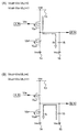
ここで、増幅回路の一例として、ソースフォロワ回路の構成とその動作について説明する。最初に図5(A)にソースフォロワ回路の構成例を示し、定常状態における動作について説明する。次いで、図5(B)(C)を用いて、ソースフォロワ回路の動作点について説明する。最後に、図6に図5(A)とは異なる構成のソースフォロワ回路の例を示し、過渡状態における動作について説明する。
【0005】
まず図5(A)にソースフォロワ回路を用いて、定常状態における動作について説明する。
【0006】
図5(A)において、11はnチャネル型の増幅用トランジスタ、12はnチャネル型のバイアス用トランジスタである。なお図5(A)に示す増幅用トランジスタ11及びバイアス用トランジスタ12はnチャネル型とするが、pチャネル型トランジスタを用いて構成してもよい。またここでは簡単のため、増幅用トランジスタ11及びバイアス用トランジスタ12は、その特性及びサイズが同一であるとし、さらに電流特性も理想的なものであるとする。つまり、増幅用トランジスタ11及びバイアス用トランジスタ12のソース・ドレイン間電圧が変化しても、飽和領域における電流値は変化しないと仮定する。
【0007】
また、増幅用トランジスタ11のドレイン領域は電源線13に接続され、ソース領域はバイアス用トランジスタ12のドレイン領域に接続している。バイアス用トランジスタ12のソース領域は、電源線14に接続されている。
【0008】
バイアス用トランジスタ12のゲート電極には、バイアス電位Vbが印加される。そして電源線13には電源電位Vddが印加され、電源線14には、接地電位Vss(=0V)が印加される。
【0009】
図5(A)に示すソースフォロワ回路において、増幅用トランジスタ11のゲート電極は、入力端子となっており、増幅用トランジスタ11のゲート電極には、入力電位Vinが入力される。また増幅用トランジスタ11のソース領域が出力端子となっており、増幅用トランジスタ11のソース領域の電位が、出力電位Voutとなる。バイアス用トランジスタ12のゲート電極にはバイアス電位Vbが印加されており、該バイアス用トランジスタ12が飽和領域で動作するときには、Ibで示す電流が流れるとする。このとき、増幅用トランジスタ11及びバイアス用トランジスタ12は直列に接続されているため、両トランジスタには同量の電流が流れる。つまり、バイアス用トランジスタ12に電流Ibが流れるときには、増幅用トランジスタ11にも電流Ibが流れる。
【0010】
ここで、ソースフォロワ回路における出力電位Voutを求めてみる。出力電位Voutは、入力電位Vinよりも増幅用トランジスタ11のゲート・ソース間電圧Vgs1の分だけ低い値となる。このとき、入力電位Vin、出力電位Vout及びゲート・ソース間電圧Vgs1の関係は、以下の式(1)を満たす。
【0011】
Vout=Vin-Vgs1・・・(1)
【0012】
そして、増幅用トランジスタ11が飽和領域で動作している場合は、増幅用トランジスタ11に電流Ibが流れるためには、増幅用トランジスタ11のゲート・ソース間電圧Vgs1がバイアス電位Vbと等しいということが必要である。そうすると、以下の式(2)の式が成立する。但し式(2)は、増幅用トランジスタ11及びバイアス用トランジスタ12が飽和領域で動作するときにのみにおいて成立する。
【0013】
Vout=Vin-Vb・・・(2)
【0014】
次いで、増幅用トランジスタ11及びバイアス用トランジスタ12の電圧と電流の関係を示した図5(B)(C)を用いて、ソースフォロワ回路の動作点について説明する。さらに詳しくは、増幅用トランジスタ11のゲート・ソース間電圧Vgs1と、バイアス用トランジスタ12のゲート・ソース間電圧Vgs2が同じ値の場合について、図5(B)を用いて説明する。次いで、増幅用トランジスタ11のゲート・ソース間電圧Vgs1と、バイアス用トランジスタ12のゲート・ソース間電圧Vgs2とが異なる値の場合であって、例えばバイアス用トランジスタ12が線形領域で動作している場合について、図5(C)を用いて説明する。
【0015】
図5(B)において、点線21は増幅用トランジスタ11のゲート・ソース間電圧Vgs1がVbであるときの電圧と電流の関係を示し、実線22はバイアス用トランジスタ12のゲート・ソース間電圧Vgs2がVbであるときの電圧と電流の関係を示す。また図5(C)において、点線21は増幅用トランジスタ11のゲート・ソース間電圧Vgs1がVb`であるときの電圧と電流の関係を示し、実線22はバイアス用トランジスタ12のゲート・ソース間電圧Vgs2がVbであるときの電圧と電流の関係を示す。
【0016】
図5(B)において、増幅用トランジスタ11のゲート・ソース間電圧Vgs1と、バイアス用トランジスタ12のゲート・ソース間電圧Vgs2が同じ値であり、さらにバイアス電位Vbと、バイアス用トランジスタ12のゲート・ソース間電圧Vgs2は同じ値であるため、増幅用トランジスタ11のゲート・ソース間電圧Vgs1は、バイアス電位Vbと同じ値である。つまり、Vgs1=Vgs2=Vbとなり、図5(B)に示すように、増幅用トランジスタ11及びバイアス用トランジスタ12は飽和領域で動作している。このとき、入力電位Vinと出力電位Voutの関係は線形となる。
【0017】
一方、図5(C)において、増幅用トランジスタ11のゲート・ソース間電圧Vgs1は、バイアス用トランジスタ12のゲート・ソース間電圧Vgs2とは異なる値である。そして、バイアス用トランジスタ12のゲート・ソース間電圧Vgs2はバイアス電位Vbと同じ値である。また、増幅用トランジスタ11のゲート・ソース間電圧Vgs1は、バイアス電位Vb'であるとする。つまり、Vgs2=Vb、Vgs1=Vb`となり、図5(C)で示すように、増幅用トランジスタ11は飽和領域で動作しており、バイアス用トランジスタ12が線形領域で動作している。このとき、入力電位Vin、出力電位Vout及びバイアス電位Vb'の関係は以下の式(3)を満たす。
【0018】
Vout=Vin-Vb'・・・(3)
【0019】
バイアス用トランジスタ12が線形領域で動作するときに流れる電流をIb'とすると、Ib'<Ibとなる。つまり、Vb'<Vbとなって、入力電位Vinと電流Ib'の両者の値は小さくなる。そうすると、バイアス電位Vb'も小さくなる。このとき入力電位Vinと出力電位Voutの関係は、非線形となる。
【0020】
以上をまとめると、定常状態におけるソースフォロワ回路において、出力電位Voutの振幅を大きくするためには、バイアス電位Vbを小さくすることが好ましい。これは以下の2つの理由による。
【0021】
1つ目の理由は、式(2)に示すように、バイアス電位Vbが小さいと、出力電位Voutを大きくすることが出来るからである。2つ目の理由は、バイアス電位Vbの値が大きい場合には、入力電位Vinを小さくすると、バイアス用トランジスタ12が線形領域で動作しやすくなってしまうからである。バイアス用トランジスタ12が線形領域で動作すると、入力電位Vinと出力電位Voutの関係は、非線形となりやすい。
【0022】
なおバイアス用トランジスタ12は、導通状態であることが必要であるため、バイアス電位Vbの値は、バイアス用トランジスタ12のしきい値電圧よりも大きい値にする必要がある。
【0023】
これまでは、ソースフォロワ回路の定常状態での動作について説明してきたが、続いて、ソースフォロワ回路の過渡状態での動作について、図6を用いて説明する。
【0024】
図6に示すソースフォロワ回路は、図5(A)の回路に容量素子15が追加して設計された構成である。容量素子15の一方の端子は増幅用トランジスタ11のソース領域に接続され、他方の端子は電源線16に接続されている。電源線16には、接地電位Vssが印加されている。
【0025】
容量素子15の両電極間の電位差は、ソースフォロワ回路の出力電位Voutと同一となる。ここでは、図6(A)を用いてVout<Vin-Vbの場合の動作について説明し、次いで図6(B)を用いてVout>Vin-Vbの場合の動作について説明する。
【0026】
まず、図6(A)を用いてVout<Vin-Vbの場合のソースフォロワ回路の過渡状態における動作について説明する。
【0027】
図6(A)において、t=0のときには、増幅用トランジスタ11のゲート・ソース間電圧Vgs1の値は、バイアス用トランジスタ12のゲート・ソース間電圧Vgs2の値よりも大きい。そのため、増幅用トランジスタ11には、大きな電流が流れて、容量素子15には急速に電荷が保持される。そうすると、出力電位Voutは大きくなり、増幅用トランジスタ11のゲート・ソース間電圧Vgs1の値は減少する。
【0028】
そして時間の経過に伴い(t=t1、t1>0)、増幅用トランジスタ11のゲート・ソース間電圧Vgs1がバイアス電位Vbに等しくなると定常状態になる。このとき、出力電位Vout、入力電位Vin及びバイアス電位Vbの関係は、上記の式(2)を満たす。
【0029】
以上をまとめると、Vout<Vin-Vbの場合には、増幅用トランジスタ11のゲート・ソース間電圧Vgs1の値が、バイアス電位Vbよりも大きいため、増幅用トランジスタ11には大きな電流が流れて、容量素子15に急速に電荷が保持される。そのため、容量素子15が所定の電荷の保持を行う時間、言い換えると容量素子15に対する信号の書き込みに要する時間は短くてすむ。
【0030】
次いで、図6(B)を用いてVout>Vin-Vbの場合のソースフォロワ回路の過渡状態における動作について説明する。
【0031】
図6(B)において、t=0のときには、増幅用トランジスタ11のゲート・ソース間電圧Vgs1は、該増幅用トランジスタ11のしきい値電圧よりも小さい値である。そのため、増幅用トランジスタ11は非導通状態にある。そして容量素子15に蓄積されていた電荷は、バイアス用トランジスタ12を介して接地電位Vssの方向に流れていき、最終的には放電される。このとき、バイアス用トランジスタ12のゲート・ソース間電圧Vgs2は、バイアス電位Vbと同じ値であるので、バイアス用トランジスタ12を流れる電流はIbとなる。
【0032】
そして時間の経過に伴い(t=t1、t1>0)、出力電位Voutが小さくなり、増幅用トランジスタ11のゲート・ソース間電圧Vgs1が大きくなる。そして増幅用トランジスタ11のゲート・ソース間電圧Vgs1がバイアス電位Vbに等しくなると、定常状態となる。このとき、出力電位Vout、入力電位Vin及びバイアス電位Vbの関係は、上記の式(2)を満たす。なお定常状態では、出力電位Voutは一定の値を保っており、容量素子15に電荷は流れない。そして、増幅用トランジスタ11及びバイアス用トランジスタ12には、電流Ibが流れる。
【0033】
以上をまとめると、Vout>Vin-Vbの場合には、容量素子15が所定の電荷の保持を行う時間、言い換えると容量素子15に対する信号の書き込み時間は、バイアス用トランジスタ12を流れる電流Ibに依存する。そして、電流Ibはバイアス電位Vbの大きさに依存する。従って、電流Ibを大きくして、容量素子15に対する信号の書き込み時間を短くするためには、バイアス電位Vbを大きくする必要が生ずる。
【0034】
なおトランジスタのしきい値電圧のバラツキを補正する方法として、信号が入力された回路の出力によりバラツキをみて、その後、そのバラツキをフィードバックさせて補正するという方法がある(例えば、非特許文献1参照。)。
【0035】
【非特許文献1】
H.Sekine et al,「Amplifier Compensation Method for a Poly-Si TFT LCLV with an Integrated Data-Driver」,IDRC'97,p.45-48
【0036】
【発明が解決しようとする課題】
上述したソースフォロワ回路の動作は、増幅用トランジスタ11及びバイアス用トランジスタ12の特性が同じであると仮定した上で行われるものである。しかし、両トランジスタは作製工程や使用する基板の相違によって生じるゲート長(L)、ゲート幅(W)及びゲート絶縁膜の膜厚のバラツキや、チャネル形成領域の結晶状態のバラツキなどの要因が重なって、しきい値電圧や移動度にバラツキが生じてしまう。
【0037】
例えば図5(A)において、増幅用トランジスタ11のしきい値電圧が3Vであり、バイアス用トランジスタ12のしきい値電圧が4Vとして、1Vのバラツキが生じていたとする。そうすると、電流Ibを流すためには、増幅用トランジスタ11のゲート・ソース間電圧Vgs1には、バイアス用トランジスタ12のゲート・ソース間電圧Vgs2よりも1V低い電圧を加える必要が生ずる。つまりVgs1=Vb-1となる。そうすると、Vout=Vin-Vgs1=Vin-Vb+1となってしまう。つまり、増幅用トランジスタ11及びバイアス用トランジスタ12のしきい値電圧に1Vでもバラツキが生じていると、出力電位Voutにもバラツキが生じてしまう。
【0038】
本発明は上記の問題点を鑑みてなされたものであり、トランジスタの特性バラツキの影響を抑制した電気回路を提供することを課題とする。さらに詳しくは、電流を増幅する機能を有する電気回路において、トランジスタの特性バラツキの影響を抑制して、所望の電圧を供給することができる電気回路を提供することを課題とする。
【0039】
【課題を解決するための手段】
本発明は、上記の問題点を解決するために、以下に示す構成の電気回路を用いる。
【0040】
最初に本発明に用いられる電気回路の構成について、図4(A)(B)を用いて説明する。図4(A)(B)において、2903、2913はスイッチング機能を有する素子であり、好ましくはトランジスタで構成されるアナログスイッチなどの半導体素子が用いられる。スイッチ2903、2913は、ON又はOFFがSignal1により制御される。なお前記スイッチ2903、2913は単なるスイッチなので、その極性は特に限定されない。
【0041】
2902と2912は整流性素子(整流素子)である。整流性素子とは、素子の両端の電極に電位差を与えたとき、単一方向にのみ電流を生ずる素子を指す。前記整流性素子は、ダイオードや、ゲート・ドレイン間を接続したTFTなどが挙げられる。なお本明細書において、ゲート・ドレイン間を接続したTFTは、ダイオード接続をしたTFTと表記する。そして、図4(A)(B)においては、整流性素子2902はダイオード接続をしたpチャネル型のトランジスタであり、整流性素子2912はダイオード接続をしたnチャネル型のトランジスタである。そして本発明では、図4(A)に示す整流性素子2902とスイッチ2903を接続した電気回路、又は図4(B)に示す整流性素子2912とスイッチ2913を接続した電気回路を用いる。
【0042】
ここで、図4(A)(B)に示した電気回路の動作について、図4(C)(D)を用いて説明する。なお、図4(C)はSignal1のタイミングチャートを示している。また図4(D)は、TFT2902、2912のゲートの電位をそれぞれVG2902、VG2912としたときのゲート・ソース間電圧と時間との関係を示している。
【0043】
ここで、電気回路の一端よりある信号が入力され、該電気回路の他端はある一定電位が与えられているとする。図4(A)に示す電気回路の場合、入力される信号をVx、一定電位をVss(≦Vx−|VthP|:VthPはTFT2902のしきい値電圧)とする。図4(B)に示す電気回路の場合、入力される信号をVx、一定電位をVdd(≧Vx+|VthN|:VthNはTFT2912のしきい値電圧)とする。
【0044】
まず、(i)で示される期間において、スイッチ2903、2913がONとなる。そうすると、図4(A)に示す電気回路において、トランジスタ2902のドレイン領域およびゲート電極の電位が低下する。図4(B)に示す電気回路おいては、トランジスタ2912のドレイン領域およびゲート電極の電位が上昇する。トランジスタ2902、2912は、いずれも両電極間の電圧がしきい値電圧の絶対値を上回っているためONである。
【0045】
次いで、(ii)で示される期間において、スイッチ2903、2913がOFFとなる。そうすると、TFT2902のドレイン電位は上昇し、TFT2912のドレイン電位は下降する。
【0046】
やがて、(iii)で示される期間において、TFT2902、2912のゲート・ソース間電圧は、そのしきい値電圧に等しくなり、TFT2902、2912はともにOFFする。このとき、TFT2902、2912のドレイン電位はそれぞれ、VX−|VthP|、VX+|VthN|となる。つまり、TFT2902、2912によって、入力される信号の電位VXに、それぞれのしきい値電圧を上乗せする動作が行われたことになる。
【0047】
上述したように、本発明は、素子の両端の電極に電位差を与えたとき、単一の方向にのみ電流が生ずる整流性素子を用いた電気回路を提供する。そして本発明は、整流性素子の一方の端子に信号電圧を入力したとき、他方の端子の電位が該整流性素子のしきい値電圧分だけオフセットをかけた電位となることを利用している。
【0048】
つまり、整流性素子間にしきい値電圧のバラツキが生じていても、該整流性素子は、常に該整流性素子のしきい値電圧分だけオフセットをかけた電位を提供できる。そして本発明は前記整流性素子を用いることにより、整流性素子間のしきい値電圧のバラツキの影響を抑制した電気回路を提供することが出来る。
【0049】
なお、TFT2902、2912の極性は特に限定されない。また、TFT2902、2912は、図4(E)に示すように、それぞれダイオード2922、2932を用いても良い。ダイオード2922、2932には、通常のPN接合を有するダイオードの他、公知の構造のダイオードを用いることが出来る。
【0050】
本発明は、トランジスタのゲートと入力電位との間に、整流素子と、該整流素子の一方の電極と第1電位との間に接続される第1スイッチとからなる補償回路が設けられ、第2電位に一方の端子が接続され、他方の端子が前記トランジスタのソースに接続される第2スイッチを有するソースフォロワ回路であって、前記整流素子の一方の電極に前記入力電位が印加されて、前記第1スイッチがオフすると、前記整流素子の他方の電極は第3電位に収束され、前記第3電位が前記トランジスタのゲート電極に入力されて、前記第2のスイッチがオンすると、前記ソースと前記第2スイッチとの間から出力電位を取り出すことを特徴とする。
【0051】
本発明は、第1トランジスタのゲートと入力電位との間に、第1整流素子と、該第1整流素子の一方の電極と第1電位との間に接続される第1スイッチとからなる第1補償回路と、
第2トランジスタのゲートとバイアス電位の間に、第2整流素子と、該第2整流素子の一方の電極と第2電位との間に接続される第2スイッチとからなる第2補償回路とが設けられたソースフォロワ回路であって、
前記第1整流素子の第1の電極に入力電位が印加されて、前記第1スイッチがオフすると、前記第1整流素子の一方の電極の電位は第3電位に収束され、
前記第2整流素子の第1の電極にバイアス電位が印加されて、前記第2スイッチがオフすると、前記第2整流素子の一方の電極の電位は第4電位に収束され、
前記第3電位が前記第1トランジスタのゲート電極に入力されて、前記第4電位が前記第2トランジスタのゲート電極に入力されると、前記第1トランジスタのソースから出力電位を取り出すことを特徴とする。
【0052】
なお本発明では、どのような材料を用いたトランジスタ、どのような手段、製造方法を経たトランジスタを用いてもよく、またどのようなタイプのトランジスタを用いてもよい。例えば、薄膜トランジスタ(TFT)を用いてもよい。TFTとしては、半導体層が非晶質(アモルファス)、多結晶(ポリクリスタル、ポリシリコン)、単結晶のいずれを用いてもよい。その他のトランジスタとして、単結晶基板において作られたトランジスタでもよいし、SOI基板において作られたトランジスタでもよい。また、有機物やカーボンナノチューブで形成されたトランジスタでもよい。さらに、MOS型トランジスタでもよいし、バイポーラ型トランジスタでもよい。
【0053】
【発明の実施の形態】
(実施の形態1)
本実施の形態では、本発明の電気回路の一例として、ソースフォロワ回路を示し、その構成と動作について図1〜図3を用いて説明する。
【0054】
最初にソースフォロワ回路の構成について、図1〜図3を用いて説明する。
【0055】
図1〜図3において、411は増幅用トランジスタであり、412はバイアス用トランジスタである。413、414は整流性素子であり、本実施の形態ではトランジスタを用いる。そして、トランジスタ413のしきい値電圧をVth1とし、トランジスタ414のしきい値電圧をVth2とする。415、416はスイッチング機能を有する素子であり、好ましくはトランジスタで構成されるアナログスイッチなどの半導体素子が用いられる。なお前記スイッチ415、416は単なるスイッチなので、その極性は特に限定されない。
【0056】
なおトランジスタ411〜トランジスタ413の極性は特に限定されないが、トランジスタ411とトランジスタ412、トランジスタ411とトランジスタ413、トランジスタ412とトランジスタ414は同じ極性であることが好ましい。そして図1と図2(A)には、トランジスタ411〜トランジスタ414がnチャネル型であるソースフォロワ回路を示す。そして、図2(B)と図3には、トランジスタ411〜トランジスタ414がpチャネル型である場合を示す。
【0057】
増幅用トランジスタ411のドレイン領域は電源線419に接続され、ソース領域は、トランジスタ412を介して電源線420に接続されている。増幅用トランジスタ411のゲート電極は、トランジスタ413のゲート電極及びドレイン領域に接続されている。なお以下には増幅用トランジスタ411は、トランジスタ411と表記する。
【0058】
バイアス用トランジスタ412のドレイン領域はトランジスタ411を介して電源線419に接続され、ソース領域は電源線420に接続されている。バイアス用トランジスタ412のゲート電極は、トランジスタ414のゲート電極及びドレイン領域に接続されている。なお以下にはバイアス用トランジスタ412は、トランジスタ412と表記する。
【0059】
スイッチ415、416は、入力される信号によって、導通又は非導通(オン又はオフ)が制御される。しかし、説明を簡単にするために、スイッチ415、416に信号を入力する信号線等の図示は省略する。
【0060】
そして、図1〜図3に示すソースフォロワ回路において、トランジスタ413のソース領域には、入力電位Vinが入力される。またトランジスタ414のソース領域にはバイアス電位が入力される。そしてトランジスタ411のソース領域の電位が出力電位Voutとなる。
【0061】
417〜420は電源線であり、電源線417には電源電位Vdd1が印加され、電源線418には電源電位Vdd2が印加される。また電源線419には、電源電位Vdd3が印加され、電源線420には接地電位Vssが印加される。なお、電源電位Vdd1と電源電位Vdd2は以下の条件を満たす必要がある。
【0062】
まず図1と図2(A)に示すように、トランジスタ411〜トランジスタ413がnチャネル型の場合には、電源電位Vdd1は入力電位Vinとトランジスタ413のしきい値電圧Vth1とを足した値以上の電位である必要がある。このとき、以下の式(4)が成立する。
【0063】
Vdd1≧(Vin+Vth1)・・・(4)
【0064】
同様に、電源電位Vdd2は、バイアス電位Vbとトランジスタ414のしきい値電圧Vth2とを足した値以上の電位である必要がある。このとき、以下の式(5)が成立する。
【0065】
Vdd2≧(Vb+Vth2)・・・(5)
【0066】
さらに、図2(B)と図3に示すように、トランジスタ411〜トランジスタ413がpチャネル型の場合には、電源電位Vdd1は入力電位Vinからトランジスタ413のしきい値電圧Vth1の絶対値を引いた値以下の電位である必要がある。このとき、以下の式(6)が成立する。
【0067】
Vdd1≦(Vin-|Vth1|)・・・(6)
【0068】
同様に、電源電位Vdd2は、バイアス電位Vbからトランジスタ414のしきい値電圧Vth2の絶対値を引いた値以下の電位である必要がある。このとき、以下の式(7)が成立する。
【0069】
Vdd2≦(Vb-|Vth2|)・・・(7)
【0070】
なお電源線417〜電源線419には、共通の1本の電源線を用いることもできる。但し、そのときには式(4)、(5)を満たす電位を印加することが必要である。同様に、式(6)、(7)を満たす電位を印加することが必要である。
【0071】
続いて、図1〜図3に示したソースフォロワ回路の動作について説明する。まず、トランジスタ411〜トランジスタ413がnチャネル型の場合について、図1と図2(A)を用いて説明する。次いで、トランジスタ411〜トランジスタ413がpチャネル型の場合について、図2(B)と図3を用いて説明する。
【0072】
図1(A)において、トランジスタ413のソース領域には、入力電位Vinが印加されており、またトランジスタ414のソース領域にはバイアス電位Vbが印加されている。そして、スイッチ415、416をオンにする。そうすると、電源線417とトランジスタ413のソース領域には電位差が生じ、電流が流れる。同様に、電源線418からトランジスタ414のソース領域には電位差が生じ、電流が流れる。このとき、トランジスタ413のゲート電極の電位は、電源電位Vdd1と同じ値となり、トランジスタ414のゲート電極の電位は、電源電位Vdd2と同じ値になる。
【0073】
次いで、スイッチ415、416をオフにする(図1(B))。そうすると、トランジスタ413、414のドレイン領域の電位は下降する。やがて、トランジスタ413、414のゲート・ソース間電圧は、該トランジスタ413、414のしきい値電圧Vth1、Vth2に等しくなる。その結果、トランジスタ413、414はともにオフになる。
【0074】
このとき、トランジスタ413のドレイン電位はVin+Vth1である。また、トランジスタ414のドレイン電位はVb+Vth2である。(図2(A))。そして、トランジスタ411のソース領域の電位が出力電位Voutとなる。前記出力電位Voutは以下の式(8)〜式(15)により算出される。
【0075】
トランジスタが、飽和領域で動作するときには、以下の式(8)が成立する。Idsはトランジスタのチャネル形成領域を流れる電流量であり、Vgsはトランジスタのゲート・ソース間電圧である。またVthはトランジスタのしきい値電圧である。
【0076】
Ids∝(Vgs−Vth)2・・・(8)
【0077】
上記の式(8)において、Vk=Vgs-Vthとすると、以下の式(9)が成立する。
【0078】
Ids∝Vk 2・・・(9)
【0079】
式(9)より、Idsは、VgsからVthの値を引いた値であるVkの2乗に比例していることがわかる。ここで、トランジスタ411、412に上記の式(8)、(9)を適用して、出力電位Voutを算出する。まずトランジスタ412のゲート電極に加えられた電圧をVa2とすると、以下の式(10)が成立する。
【0080】
Va2=Vb+Vth2・・・(10)
【0081】
次に、トランジスタ412とトランジスタ414のしきい値電圧が等しいと仮定する。そして、トランジスタ412のゲート電極に加えられた電圧Va2からしきい値電圧Vth2を引いた値をVk2とすると、以下の式(11)が成立する。
【0082】
Vk2=Va2-Vth2=(Vb+Vth2)-Vth2=Vb・・・(11)
【0083】
また、トランジスタ411のゲート電極に加えられた電圧をVa1とすると、以下の式(12)が成立する。
【0084】
Va1=Vin+Vth1・・・(12)
【0085】
トランジスタ413とトランジスタ411のしきい値電圧が等しいと仮定する。そして、トランジスタ411のゲート・ソース間電圧Vgs1からしきい値電圧Vth1を引いた値をVk1とすると、以下の式(13)が成立する。
【0086】
Vk1=Vgs1-Vth1・・・(13)
【0087】
ここで、トランジスタ411、412には同量の電流が流れることを考慮すると、以下の式(14)が成立する。なお本実施の形態では、簡単のため、トランジスタ411とトランジスタ412は、ゲート幅、ゲート長などのサイズが同じであるとする。
【0088】
Vk1=Vk2=Vb・・・(14)
【0089】
そして、出力電位Voutは、トランジスタ211のソース領域の電位であることから、以下の式(15)が成立する。
【0090】
Vout=Va1-Vgs1=(Vin+Vth1)-(Vb+Vth1)=Vin-Vb・・・(15)
【0091】
式(15)に示すように、出力電位Voutは、入力電位Vinからバイアス電位Vbを引いた値になっており、しきい値電圧には依存していない。そのため、トランジスタ411、415のしきい値電圧にバラツキが生じていても、出力電位Voutに対する影響を抑制することが出来る。
【0092】
次いで、トランジスタ411〜トランジスタ413がpチャネル型の場合について、図2(B)と図3を用いて説明する。
【0093】
図2(B)において、トランジスタ413のソース領域には、入力電位Vinが印加されており、またトランジスタ414のソース領域にはバイアス電位Vbが印加されている。そして、スイッチ415、416をオンにする。そうすると、トランジスタ413のソース領域と電源線417には電位差が生じ、電流が流れる。同様に、トランジスタ414のソース領域と電源線418には電位差が生じ、電流が流れる。そして、トランジスタ413のゲート電極の電位は、電源電位Vdd1と同じ値となり、トランジスタ414のゲート電極の電位は、電源電位Vdd2と同じ値になる。
【0094】
次いで、スイッチ415、416をオフにする(図3(A))。そうすると、トランジスタ413、414のドレイン領域の電位は上昇する。やがて、トランジスタ413、414のゲート・ソース間電圧は、該トランジスタ413、414のしきい値電圧Vth1、Vth2に等しくなる。その結果、トランジスタ413、414はともにオフになる。
【0095】
このとき、トランジスタ413のドレイン電位は(Vin-|Vth1|)である。また、トランジスタ414のドレイン電位は(Vb-|Vth2|)である(図3(B))。そして、トランジスタ411のソース領域の電位が出力電位となる。前記出力電位は以下の式(16)〜式(21)により算出される。
【0096】
まず、上記の式(8)、(9)を参照して、トランジスタ412のゲート電極に加えられた電圧をVa2とすると、以下の式(16)が成立する。
【0097】
Va2= Vb-|Vth2|・・・(16)
【0098】
さらに、トランジスタ412のゲート電極に加えられた電圧Va2からしきい値電圧Vth2を引いた値をVk2とすると、以下の式(17)が成立する。
【0099】
Vk2=Va2-Vth2=(Vb-|Vth2|)-|Vth2|=Vb・・・(17)
【0100】
また、トランジスタ411のゲート電極に加えられた電圧をVa1とすると、以下の式(18)が成立する。
【0101】
Va1=Vin-|Vth1|・・・(18)
【0102】
さらに、トランジスタ411のゲート・ソース間電圧Vgs1からしきい値電圧Vth1を引いた値をVk1とすると、以下の式(19)が成立する。
【0103】
Vk1=Vgs1-|Vth1|・・・(19)
【0104】
ここで、トランジスタ411、412には同量の電流が流れることを考慮すると、以下の式(20)が成立する。
【0105】
Vk1=Vk2=Vb・・・(20)
【0106】
そして、出力電位Voutは、トランジスタ211のソース領域の電位であることから、以下の式(21)が成立する。
【0107】
Vout=Va1-Vgs1=(Vin+Vth1)-(Vb+Vth1)=Vin-Vb・・・(21)
【0108】
式(21)に示すように、出力電位Voutは、入力電位Vinからバイアス電位Vbを引いた値になっており、しきい値電圧には依存していない。そのため、トランジスタ411、415のしきい値電圧にバラツキが生じていても、出力電位Voutに対する影響を抑制することが出来る。
【0109】
また図7(A)には、図1と図2(A)に示したソースフォロワ回路において、トランジスタ412、414と、スイッチ416と、電源線418とを配置していない場合のソースフォロワ回路を示す。なお図7(A)に示す電気回路において、電源線420とトランジスタ411のソース領域との間には、スイッチ423が追加して配置されている。図7(A)に示すソースフォロワ回路の動作は、上述した図1と図2(A)に示したソースフォロワ回路の動作と同じであるので、本実施の形態では説明を省略する。
【0110】
さらに図7(B)には、図2(B)と図3に示したソースフォロワ回路において、トランジスタ412、414と、スイッチ416と、電源線418とを配置していない場合のソースフォロワ回路を示す。なお、図7(B)に示すソースフォロワ回路の動作は、上述した図2(B)と図3に示したソースフォロワ回路の動作と同じであるので、本実施の形態では説明は省略する。
【0111】
なお本明細書では、整流性素子に所定の電荷を与える動作を設定動作とよぶ。本実施の形態では、図1(A)に示す動作、図2(B)に示す動作が設定動作に相当する。入力電位Vinを入力して、出力電位Voutを取り出す動作を出力動作とよぶ。本実施の形態では、図1(B)及び図2(A)に示す動作、図3(A)(B)に示す動作が出力動作に相当する。
【0112】
上述したように、本発明は、素子の両端の電極に電位差を与えたとき、単一の方向にのみ電流が生ずる整流性素子を用いた電気回路を提供する。そして本発明は、整流性素子の一方の端子に信号電圧を入力したとき、他方の端子の電位が該整流性素子のしきい値電圧分だけオフセットをかけた電位となることを利用している。
【0113】
つまり、整流性素子間にしきい値電圧のバラツキが生じていても、該整流性素子は、常に該整流性素子のしきい値電圧分だけオフセットをかけた電位を提供できる。本発明は前記整流性素子を用いることにより、整流性素子間のしきい値電圧のバラツキの影響を抑制した電気回路を提供することが出来る。そして、整流性素子間のしきい値電圧のバラツキの影響を抑制するということは、トランジスタのしきい値電圧のバラツキの影響を抑制した電気回路を提供することが出来ることに相当する。
【0114】
(実施の形態2)
前述した実施の形態1では、本発明を適用したソースフォロワ回路について説明した。しかし本発明は、差動増幅回路、センスアンプ、オペアンプなどに代表される演算回路など、さまざまな回路にも適用することが出来る。本実施の形態では、本発明を適用した演算回路について図8〜図11を用いて説明する。
【0115】
まず、本発明を適用した差動増幅回路について、図8を用いて説明する。差動増幅回路では、入力電位Vin1及び入力電位Vin2の差の演算を行って出力電位Voutを出力する。
【0116】
図8に示す差動増幅回路において、272、273はpチャネル型のトランジスタであり、274〜276はnチャネル型のトランジスタである。277〜279は整流性素子であり、本実施の形態ではnチャネル型のトランジスタを用いる。また、280〜282は、スイッチング機能を有する素子であり、スイッチと表記する。スイッチ280〜スイッチ282には、好ましくはトランジスタなどの半導体素子が用いられる。なお前記スイッチ280〜スイッチ282は単なるスイッチなので、その極性は特に限定されない。
【0117】
トランジスタ272のドレイン領域は電源線285に接続され、ソース領域はトランジスタ274のドレイン領域に接続されている。トランジスタ273のドレイン領域は電源線285に接続され、ソース領域はトランジスタ275のドレイン領域に接続されている。トランジスタ272のゲート電極とトランジスタ273のゲート電極は接続されている。なおトランジスタ272及びトランジスタ273の代わりに、抵抗を配置してもよい。
【0118】
トランジスタ274のドレイン領域は、トランジスタ272を介して電源線285に接続され、ソース領域はトランジスタ276を介して電源線289に接続されている。トランジスタ274のゲート電極は、トランジスタ277のゲート電極に接続されている。
【0119】
トランジスタ275のドレイン領域は、トランジスタ273を介して電源線285に接続され、ソース領域はトランジスタ276を介して電源線289に接続されている。トランジスタ275のゲート電極は、トランジスタ278のゲート電極に接続されている。
【0120】
トランジスタ276のドレイン領域は、トランジスタ274のソース領域及びトランジスタ275のソース領域に接続されている。トランジスタ276のソース領域は電源線289に接続され、ゲート電極はトランジスタ279のゲート電極に接続されている。
【0121】
図8に示す差動増幅回路においては、トランジスタ277のソース領域には入力電位Vin1が入力され、トランジスタ278のソース領域には入力電位Vin2が入力される。またトランジスタ279のソース領域にはバイアス電位Vbが入力される。そしてトランジスタ275のドレイン領域の電位が出力電位Voutとなる。
【0122】
285〜289は電源線であり、電源線285には電源電位Vdd1が印加され、電源線286には電源電位Vdd2が印加される。また電源線287には電源電位Vdd3が印加され、電源線288には電源電位Vdd4が印加される。また電源線289には接地電位Vssが印加される。ここで、トランジスタ277のしきい値電圧をVth277、トランジスタ278のしきい値電圧をVth278、トランジスタ279のしきい値電圧をVth279とすると、各電源電位Vdd2〜Vdd4は以下の式(22)〜(24)を満たすことが必要となる。
【0123】
Vdd2≧(Vin1+Vth277)・・・(22)
【0124】
Vdd3≧(Vin2+Vth278)・・・(23)
【0125】
Vdd4≧(Vb+Vth279)・・・(24)
【0126】
なお電源線285〜電源線288には、共通の1本の電源線を用いることもできる。但し、そのときには式(22)〜(24)を満たす電位を印加することが必要である。また図8に示した差動増幅回路の動作の説明は、上述した実施の形態1に準ずるので本実施の形態では省略する。
【0127】
続いて、図8に示す差動増幅回路を構成するトランジスタが逆の導電型を有する場合について、図9を用いて説明する。
【0128】
図9に示す差動増幅回路において、272、273がnチャネル型のトランジスタであり、274〜276がpチャネル型のトランジスタである。277〜279は整流性素子であり、本実施の形態ではpチャネル型のトランジスタを用いる。また、280〜282はスイッチである。なおトランジスタ272〜トランジスタ279の接続の関係は、上述した図8に示した差動増幅回路と同じであるので、ここでは説明は省略する。
【0129】
285〜289は電源線であり、電源線285には電源電位Vdd1が印加され、電源線286には電源電位Vdd2が印加される。また電源線287には電源電位Vdd3が印加され、電源線288には電源電位Vdd4が印加される。また電源線289には接地電位Vssが印加される。ここで、電圧をVth279とすると、各電源電位Vdd2〜Vdd4は以下の式(25)〜(27)を満たすことが必要となる。
【0130】
Vdd2≦(Vin1-|Vth277|)・・・(25)
【0131】
Vdd3≦(Vin2-|Vth278|)・・・(26)
【0132】
Vdd4≦(Vb-|Vth279|)・・・(27)
【0133】
なお電源線285〜電源線288には、共通の1本の電源線を用いることもできる。但し、そのときには式(25)〜(27)を満たす電位を印加することが必要である。また図9に示した差動増幅回路の動作の説明は、上述した実施の形態1に準ずるので本実施の形態では省略する。
【0134】
また本実施の形態では、図8、9に示す電気回路を差動増幅回路として示したが、本発明はこれに限定されず、入力電位Vin1と入力電位Vin2として入力する電圧を適宜変更して、センスアンプなどの他の演算回路として用いることも出来る。
【0135】
次いで、本発明を適用したオペアンプについて、図10、11を用いて説明する。図10(A)にはオペアンプの回路記号を示し、図10(B)には該オペアンプの回路構成を示す。
【0136】
なお、オペアンプの回路構成としては、さまざまなものがある。そこで、図12では、もっとも簡単な場合として、差動増幅回路にソースフォロワ回路を組み合わせた場合について述べる。よって、オペアンプの回路構成は、図12の構成に限定されない。
【0137】
オペアンプでは、入力電位Vin1及び入力電位Vin2と、出力電位Voutとの関係によって特性が定義される。より詳しくは、オペアンプは、入力電位Vin1及び入力電位Vin2との差の電圧に対し、増幅度Aを掛けて出力電位Voutを出力する機能を有する。
【0138】
図10(B)に示すオペアンプにおいて、トランジスタ277のソース領域には入力電位Vin1が入力され、トランジスタ278のソース領域には入力電位Vin2が入力される。またトランジスタ279、414のソース領域にはバイアス電位Vbが入力される。そしてトランジスタ411のソース領域の電位が出力電位Voutとなる。
【0139】
図10(B)に示す回路において、305で示す点線で囲んだ部分は、図8に示した差動増幅回路と同じ構成である。また、306で示す点線で囲んだ部分は、図1に示したソースフォロワ回路と同じ構成である。そのため、図10(B)に示したオペアンプの詳しい構成の説明は省略する。但し、電源線286〜電源線288に印加される各電源電位は、上記の式(22)〜(24)を満たす必要がある。また、電源線417、418に印加される各電源電位は、上記の式(4)、(5)を満たす必要がある。なお本実施の形態では、上記の式(4)における入力電位Vinとは、トランジスタ275のドレイン領域の電位に相当する。
【0140】
また図11には、トランジスタ412がpチャネル型である場合のオペアンプを示す。図11(B)において、トランジスタ414のドレイン領域が、トランジスタ413のドレイン領域に接続されている点以外は、図10(B)に示すオペアンプの構成と同じである。そのため、図11(B)に示したオペアンプの詳しい構成の説明は省略する。但し、電源線286〜電源線288に印加される各電源電位は、上記の式(22)〜(24)を満たす必要がある。また、電源線417に印加される電源電位は、上記の式(4)を満たす必要がある。なお本実施の形態では、上記の式(4)における入力電位Vinとは、トランジスタ275のドレイン領域の電位に相当する。さらに、電源線418に印加される電源電位は、以下の式(28)を満たす必要がある。
【0141】
【数1】
Vdd6≦(Vin-|Vth414|)・・・(28)
【0142】
このように本発明は、素子の両端の電極に電位差を与えたとき、単一の方向にのみ電流が生ずる整流性素子を用いた電気回路を提供する。そして本発明は、整流性素子の一方の端子に信号電圧を入力したとき、他方の端子の電位が該整流性素子のしきい値電圧分だけオフセットをかけた電位となることを利用している。
【0143】
つまり、整流性素子間にしきい値電圧のバラツキが生じていても、該整流性素子は、常に該整流性素子のしきい値電圧分だけオフセットをかけた電位を提供できる。本発明は前記整流性素子を用いることにより、整流性素子間のしきい値電圧のバラツキの影響を抑制した電気回路を提供することが出来る。そして、整流性素子間のしきい値電圧のバラツキの影響を抑制するということは、トランジスタのしきい値電圧のバラツキの影響を抑制した電気回路を提供することが出来ることに相当する。
【0144】
なお本実施の形態は、実施の形態1と任意に組み合わせることが可能である。
【0145】
(実施の形態3)
本実施の形態では、本発明を適用した光電変換素子を有する半導体装置の構成とその動作について、図12、13を用いて説明する。
【0146】
図12(A)に示す半導体装置は、基板701上に、複数の画素がマトリクス状に配置された画素部702を有し、画素部702の周辺には、信号線駆動回路703、第1〜第4の走査線駆動回路704〜707を有する。図12(A)に示す半導体装置は、信号線駆動回路703と、4組の走査線駆動回路704〜707を有しているが、本発明はこれに限定されず、信号線駆動回路と走査線駆動回路の数は画素の構成に応じて任意に配置することが出来る。また、信号線駆動回路703と、第1〜第4の走査線駆動回路704〜707には、FPC708を介して外部より信号が供給されている。しかし本発明はこれに限定されず、画素部702以外の電気回路は、ICなどを用いて外部から供給するようにしてもよい。
【0147】
最初に、第1の走査線駆動回路704及び第2の走査線駆動回路705の構成について、図12(B)を用いて説明する。第3の走査線駆動回路706及び第4の走査線駆動回路707は、図12(B)の図に準ずるので、図示は省略する。
【0148】
第1の走査線駆動回路704は、シフトレジスタ709、バッファ710を有する。第2の走査線駆動回路705は、シフトレジスタ711、バッファ712を有する。動作を簡単に説明すると、シフトレジスタ709、711は、クロック信号(G-CLK)、スタートパルス(SP)及びクロック反転信号(G-CLKb)に従って、順次サンプリングパルスを出力する。その後バッファ710、712で増幅されたサンプリングパルスは、走査線に入力されて、1行ずつ選択状態にしていく。
【0149】
なおシフトレジスタ709とバッファ710との間、又はシフトレジスタ711とバッファ712との間にはレベルシフタ回路を配置した構成にしてもよい。レベルシフタ回路を配置することによって、電圧振幅を大きくすることが出来る。
【0150】
次いで、信号線駆動回路703の構成について、図12(C)を用いて説明する。
【0151】
信号線駆動回路703は、信号出力線用駆動回路715、サンプルホールド回路716、バイアス回路714及び増幅回路717を有する。バイアス回路714は、各画素の増幅用トランジスタと対になって、ソースフォロワ回路を形成する。サンプルホールド回路716は、信号を一時的に保存したり、アナログ・デジタル変換を行ったり、雑音を低減したりする機能を有する。信号出力用駆動回路715は、一時的に保存されていた信号を、順に出力していくための信号を出力する機能を有する。そして、増幅回路717は、サンプルホールド回路716と信号出力用駆動回路715により出力された信号を増幅する回路を有する。なお、増幅回路717は、信号を増幅する必要のない場合には配置しなくてもよい。
【0152】
そして、画素部702においてi列目j行目に配置される画素713の回路と、i列目の周辺のバイアス回路714の構成とその動作について、図13を用いて説明する。
【0153】
最初に、i列目j行目に配置される画素713の回路と、i列目の周辺のバイアス回路714の構成について説明する。
【0154】
図13に示す画素713は、第1〜第4の走査線Ga(j)〜Gd(j)、信号線S(i)、第1の電源線Va(i)、第2の電源線Vc(i)を有する。また、nチャネル型のトランジスタ254、255、光電変換素子257、スイッチ250〜スイッチ253を有する。トランジスタ254はダイオード接続をしており、整流性素子に相当する。
【0155】
バイアス回路714は、nチャネル型のトランジスタ256、257、スイッチ258を有する。トランジスタ257はダイオード接続をしており、整流性素子に相当する。
【0156】
本実施の形態においては、トランジスタ255はnチャネル型としたが、本発明はこれに限定されず、pチャネル型でもよい。但し、トランジスタ255とトランジスタ260により、ソースフォロワ回路を形成するので、両トランジスタは同じ極性であることが好ましい。
【0157】
スイッチ250〜254、258は、スイッチング機能を有する半導体素子であり、好ましくはトランジスタが用いられる。スイッチ251は、第1の走査線Ga(j)から入力される信号により、オン又はオフが制御される。スイッチ250は、第2の走査線Gb(j)から入力される信号により、オン又はオフが制御される。スイッチ252は、第3の走査線Gc(j)から入力される信号により、オン又はオフが制御される。スイッチ253は、第4の走査線Gd(j)から入力される信号により、オン又はオフが制御される。またスイッチ258も入力される信号によって、導通又は非導通(オン又はオフ)が制御される。しかし、説明を簡単にするために、スイッチ258に信号を入力する信号線の図示は省略する。
【0158】
画素713において、トランジスタ255のソース領域とドレイン領域は、一方は第1の電源線Va(i)に接続され、他方はスイッチ250を介して信号線S(i)に接続されている。トランジスタ255のゲート電極は、トランジスタ254のドレイン領域及びゲート電極に接続されている。光電変換素子257の一方の端子は、スイッチ252を介してトランジスタ254のソース領域に接続されている。光電変換素子257の他方の端子は電源線258に接続されている。電源線258には、接地電位Vssが印加される。
【0159】
また、バイアス回路714において、トランジスタ256のドレイン領域は信号線S(i)に接続され、ソース領域は電源線260に接続されている。電源線260には、接地電位Vssが印加される。またトランジスタ256のゲート電極は、トランジスタ257のゲート電極及びドレイン領域に接続され、且つスイッチ258を介して電源線259に接続されている。電源線259には、電源電位Vddが印加される。また、トランジスタ257のソース領域には、バイアス電位Vbが印加される。
【0160】
そして、図13において、719で示す点線で囲んだ部分と714で示す点線で囲んだ部分とが、図1で示したソースフォロワ回路に相当する。このとき、第2の電源線Vc(i)の電位は、以下の式(29)を満たす必要がある。なお式(29)において、Vpdとは光電変換素子257から読み出される信号の電位であり、Vth254とはトランジスタ254のしきい値電圧である。
【0161】
Vc≧(Vpd+Vth254)・・・(29)
【0162】
同様に、電源線259の電位Vddは、以下の式(30)を満たす必要がある。なお式(30)において、Vth257とはトランジスタ257のしきい値電圧である。
【0163】
Vdd≧(Vb+Vth257)・・・(30)
【0164】
なお上記の式(29)、(30)は、トランジスタ254、255、256、257がnチャネル型の場合において成立する。ここで、トランジスタ254、255、256、257がpチャネル型の場合には、以下の式(31)、(32)が成立する。
【0165】
Vc≦(Vpd-|Vth254|)・・・(31)
【0166】
Vdd≦(Vb-|Vth257|)・・・(32)
【0167】
次いで、i列目j行目に配置される画素713の回路と、i列目の周辺のバイアス回路714の動作を簡単に説明する。
【0168】
まず、画素713においてスイッチ251をオンにする。そしてそれ以外のスイッチはオフにする。そうすると、第2の電源線Vc(i)の電位と、トランジスタ254、255のゲート電極の電位が同じになる。その結果、トランジスタ254、255はオンになる。
【0169】
同様に、バイアス回路714においてスイッチ258をオンにする。そうすると、電源線259の電源電位Vddと、トランジスタ256、257のゲート電極の電位が同じになる。その結果、トランジスタ256、257はオンになる。
【0170】
次いで、スイッチ252をオンにする。このとき、スイッチ251、258はオンであり、その以外のスイッチはオフを維持する。このとき、光電変換素子257から読み出される信号の電位をVpdとする。
【0171】
続いて、画素713においてスイッチ251をオフにする。そうすると、トランジスタ254のドレイン電位は下降する。そして、トランジスタ254のゲート・ソース間電圧は、該トランジスタ254のしきい値電圧に等しくなり、トランジスタ254はオフになる。このとき、トランジスタ254のドレイン電位は、Vpd+Vth254となっている。つまり、トランジスタ254によって、入力される信号の電位Vpdに、該トランジスタ254のしきい値電圧Vth254を上乗せする動作が行われたことになる。なおスイッチ252は、トランジスタ254がオフになった後に、オンからオフにするとよい。
【0172】
同様に、バイアス回路714においてスイッチ258をオフにする。そうすると、トランジスタ257のドレイン電位は下降する。そして、トランジスタ257のゲート・ソース間電圧は、該トランジスタ257のしきい値電圧に等しくなり、トランジスタ257はオフになる。このとき、トランジスタ257のドレイン電位は、Vb+Vth257となっている。つまり、トランジスタ257によって、入力される信号の電位Vbに、該トランジスタ257のしきい値電圧Vth257を上乗せする動作が行われたことになる。
【0173】
次いで、スイッチ250をオンにする。そしてそれ以外のスイッチはオフとする。そうすると、トランジスタ255のソース領域の電位が出力電位Voutとなり、該出力電位Voutは、光電変換素子257により読み取られた信号として、スイッチ250を介して信号線S(i)に出力される。
【0174】
続いて、スイッチ253をオンにして、それ以外のスイッチは全てオフにする。そして、光電変換素子257を初期化する。より詳しくは、光電変換素子257のnチャネル側端子の電位が電源線258の電位と同じになるように、光電変換素子257が保持している電荷をスイッチ254を介して、電源線V(i)の方向に流れるようにする。以後、上記の動作を繰り返す。
【0175】
上述したように、本発明は、素子の両端の電極に電位差を与えたとき、単一の方向にのみ電流が生ずる整流性素子を用いた電気回路を提供する。そして本発明は、整流性素子の一方の端子に信号電圧を入力したとき、他方の端子の電位が該整流性素子のしきい値電圧分だけオフセットをかけた電位となることを利用している。
【0176】
つまり、整流性素子間にしきい値電圧のバラツキが生じていても、該整流性素子は、常に該整流性素子のしきい値電圧分だけオフセットをかけた電位を提供できる。本発明は前記整流性素子を用いることにより、整流性素子間のしきい値電圧のバラツキの影響を抑制した電気回路を提供することが出来る。そして、整流性素子間のしきい値電圧のバラツキの影響を抑制するということは、トランジスタのしきい値電圧のバラツキの影響を抑制した半導体装置を提供することが出来ることに相当する。
【0177】
本発明は、実施の形態1〜実施の形態3と任意に組み合わせることが可能である。
【0178】
(実施の形態4)
本実施の形態では、本発明を適用した電気回路において、実施の形態2、3とは異なる例について、図14〜図17を用いて説明する。
【0179】
図14(A)において、310は図1と図2(A)で示したソースフォロワ回路に、スイッチ421、422を追加した構成になっている。ソースフォロワ回路310の回路構成と動作は、図1と図2(A)と同じであるので、本実施の形態では説明は省略する。
【0180】
ソースフォロワ回路310の動作は、大別して設定動作と出力動作に分別できることは上述した。なお設定動作とは、整流性素子に所定の電荷を与える動作であり、図1(A)に示す動作に相当する。また出力動作とは、入力電位Vinを入力して、出力電位Voutを取り出す動作のことであり、図1(B)と図2(A)に示す動作に相当する。
【0181】
ソースフォロワ回路310において、端子aが入力端子に相当し、端子bが出力端子に相当する。そして、スイッチ415、416は端子cから入力される信号により制御される。スイッチ421、422は端子dから入力される信号により制御される。
【0182】
なお、本形態には図1と図2(A)に示す回路を適用したが、図2(B)や図7(A)、(B)に示す回路を用いてもよい。
【0183】
そして、ソースフォロワ回路310を有する電気回路を設計するときには、図14(B)に示すように、少なくとも2つのソースフォロワ回路315、316を配置するとよい。そしてソースフォロワ回路315、316のうち、一方は設定動作を行って、他方は出力動作を行うようにするとよい。そうすると、同時に2つのことができ、動作に無駄がなく、無駄な時間が必要なくなるので、電気回路の動作をより高速で行うことができる。
【0184】
例えば、信号線駆動回路にソースフォロワ回路を用いて設計するときには、信号線ごとに少なくとも2個のソースフォロワ回路を配置するとよい。また走査線駆動回路にソースフォロワ回路を用いて設計するときには、走査線ごとに少なくとも2個のソースフォロワ回路を配置するとよい。また画素にソースフォロワ回路を用いて設計するときには、画素ごとに少なくとも2つのソースフォロワ回路を配置するとよい。
【0185】
また図14(B)において、311〜314はスイッチである。スイッチ311、312がオンのときは、スイッチ313、314はオフとなる。スイッチ311、312がオフのときには、スイッチ313、314はオンとなる。このようにして、2つのソースフォロワ回路315、316のうち、一方は設定動作を行って、他方は出力動作を行うようにする。なお、スイッチ311〜スイッチ314を配置せずに、ソースフォロワ回路310が有するスイッチ421、422を制御することによって、2つのソースフォロワ回路315、316を制御するようにしてもよい。
【0186】
また本実施の形態では、点線で囲んだ部分315、316は、ソースフォロワ回路に相当するとしたが、本発明はこれに限定されず、図8〜図11などに示した差動増幅回路、オペアンプなどを適用してもよい。
【0187】
そして本実施の形態では、信号線ごとに少なくとも2個のソースフォロワ回路を配置した信号線駆動回路の構成とその動作について、図15〜図17を用いて説明する。
【0188】
図15には信号線駆動回路を示しており、該信号線駆動回路は、シフトレジスタ321、第1のラッチ回路322、第2のラッチ回路323、D/A変換回路324及び信号増幅回路325を有する。
【0189】
なお、第1のラッチ回路322や第2のラッチ回路323が、アナログデータを保存できる回路である場合は、D/A変換回路324は省略できる場合が多い。また、信号線に出力するデータが2値、つまり、デジタル量である場合は、D/A変換回路324は省略できる場合が多い。また、D/A変換回路324には、ガンマ補正回路が内蔵されている場合もある。このように、信号線駆動回路は、図17に限定されない。
【0190】
動作を簡単に説明すると、シフトレジスタ321は、フリップフロップ回路(FF)等を複数列用いて構成され、クロック信号(S-CLK)、スタートパルス(SP)、クロック反転信号(S-CLKb)が入力される、これらの信号のタイミングに従って、順次サンプリングパルスが出力される。
【0191】
シフトレジスタ321より出力されたサンプリングパルスは、第1のラッチ回路322に入力される。第1のラッチ回路322には、ビデオ信号が入力されており、サンプリングパルスが入力されるタイミングに従って、各列でビデオ信号を保持していく。
【0192】
第1のラッチ回路322において、最終列までビデオ信号の保持が完了すると、水平帰線期間中に、第2のラッチ回路323にラッチパルス(Latch Pulse)が入力され、第1のラッチ回路322に保持されていたビデオ信号は、一斉に第2のラッチ回路323に転送される。その後、第2のラッチ回路323に保持されたビデオ信号は、1行分が同時に、D/A変換回路324へと入力される。そして、D/A変換回路324から入力される信号は信号増幅回路325へ入力される。
【0193】
第2のラッチ回路323に保持されたビデオ信号がD/A変換回路324に入力されている間、シフトレジスタ321においては再びサンプリングパルスが出力される。以後、この動作を繰り返す。
【0194】
そして、i列目から(i+2)列目の3本信号線の周辺の信号増幅回路325の構成を図16を用いて説明する。
【0195】
信号増幅回路325は、列ごとに2つのソースフォロワ回路315、316を有する。ソースフォロワ回路315、316は、それぞれ端子a〜端子dまでの4つの端子を有する。端子aはソースフォロワ回路315、316における入力端子に相当し、端子bはソースフォロワ回路315、316における出力端子に相当する。また、端子cから入力される信号によりスイッチ415、416が制御され、端子dから入力される信号によりスイッチ421、422が制御される。
【0196】
また図16に示す信号増幅回路325において、設定用信号線326と、ソースフォロワ回路315、316との間には、327、328で示す論理演算子(インバータ)が配置されている。そして、端子c、dには、設定用信号線327から出力される信号、又は上記の論理演算子の出力端子から出力される信号のどちらかが入力される。
【0197】
次いで、設定用信号線326で示す信号線から出力される信号と、ソースフォロワ回路315、316において、端子c〜端子eを介して各スイッチに入力される信号を図17を用いて説明する。
【0198】
なお、端子c、dを介して信号が入力されるスイッチは、Highの信号が入力されるとオンになり、Lowの信号が入力されるとオフになるとする。
【0199】
そして、設定用信号線326からは、図17に示すような信号が入力される。そして、ソースフォロワ回路315における端子cには、設定用信号線326から出力される信号がそのまま入力される。端子dにはインバータ327の出力端子から出力される信号が入力される。そうすると、ソースフォロワ回路315では、設定動作と出力動作のどちらか一方の動作を行うように制御することが出来る。
【0200】
同様に、ソースフォロワ回路316における端子cには、インバータ328の出力端子から出力される信号が入力される。端子dには、設定用信号線326から出力される信号がそのまま入力される。そうすると、ソースフォロワ回路316では、設定動作と出力動作のどちらか一方の動作を行うように制御することが出来る。
【0201】
上述したように、本発明は、素子の両端の電極に電位差を与えたとき、単一の方向にのみ電流が生ずる整流性素子を用いた電気回路を提供する。そして本発明は、整流性素子の一方の端子に信号電圧を入力したとき、他方の端子の電位が該整流性素子のしきい値電圧分だけオフセットをかけた電位となることを利用している。
【0202】
つまり、整流性素子間にしきい値電圧のバラツキが生じていても、該整流性素子は、常に該整流性素子のしきい値電圧分だけオフセットをかけた電位を提供できる。本発明は前記整流性素子を用いることにより、整流性素子間のしきい値電圧のバラツキの影響を抑制した電気回路を提供することが出来る。そして、整流性素子間のしきい値電圧のバラツキの影響を抑制するということは、トランジスタのしきい値電圧のバラツキの影響を抑制した電気回路を提供することが出来ることに相当する。
【0203】
なお、この信号線駆動回路の各信号線の先には、複数の画素が接続されている場合が多い。当該画素は、信号線から入力される電圧によって、状態を変化させるものであることが多い。例としては、LCDや有機ELなどがあげられる。その他にも、さまざまな構成の画素を接続することが可能である。
【0204】
なお、本実施の形態は、実施の形態1〜実施の形態4と任意に組み合わせることが可能である。
【0205】
(実施の形態5)
本発明の電気回路を用いた電子機器として、ビデオカメラ、デジタルカメラ、ゴーグル型ディスプレイ(ヘッドマウントディスプレイ)、ナビゲーションシステム、音響再生装置(カーオーディオ、オーディオコンポ等)、ノート型パーソナルコンピュータ、ゲーム機器、携帯情報端末(モバイルコンピュータ、携帯電話、携帯型ゲーム機または電子書籍等)、記録媒体を備えた画像再生装置(具体的にはDigital Versatile Disc(DVD)等の記録媒体を再生し、その画像を表示しうるディスプレイを備えた装置)などが挙げられる。それらの電子機器の具体例を図18に示す。
【0206】
図18(A)は発光装置であり、筐体3001、支持台3002、表示部3003、スピーカー部3004、ビデオ入力端子3005等を含む。本発明は表示部3003を構成する電気回路に用いることができる。また本発明により、図18(A)に示す発光装置が完成される。発光装置は自発光型であるためバックライトが必要なく、液晶ディスプレイよりも薄い表示部とすることができる。なお、発光装置は、パソコン用、TV放送受信用、広告表示用などの全ての情報表示用表示装置が含まれる。
【0207】
図18(B)はデジタルスチルカメラであり、本体3101、表示部3102、受像部3103、操作キー3104、外部接続ポート3105、シャッター3106等を含む。本発明は、表示部3102を構成する電気回路に用いることができる。また本発明により、図18(B)に示すデジタルスチルカメラが完成される。
【0208】
図18(C)はノート型パーソナルコンピュータであり、本体3201、筐体3202、表示部3203、キーボード3204、外部接続ポート3205、ポインティングマウス3206等を含む。本発明は、表示部3203を構成する電気回路に用いることができる。また本発明により、図18(C)に示す発光装置が完成される。
【0209】
図18(D)はモバイルコンピュータであり、本体3301、表示部3302、スイッチ3303、操作キー3304、赤外線ポート3305等を含む。本発明は、表示部3302を構成する電気回路に用いることができる。また本発明により、図18(D)に示すモバイルコンピュータが完成される。
【0210】
図18(E)は記録媒体を備えた携帯型の画像再生装置(具体的にはDVD再生装置)であり、本体3401、筐体3402、表示部A3403、表示部B3404、記録媒体(DVD等)読み込み部3405、操作キー3406、スピーカー部3407等を含む。表示部A3403は主として画像情報を表示し、表示部B3404は主として文字情報を表示するが、本発明は、表示部A、B3403、3404を構成する電気回路に用いることができる。なお、記録媒体を備えた画像再生装置には家庭用ゲーム機器なども含まれる。また本発明により、図18(E)に示すDVD再生装置が完成される。
【0211】
図18(F)はゴーグル型ディスプレイ(ヘッドマウントディスプレイ)であり、本体3501、表示部3502、アーム部3503を含む。本発明は、表示部3502を構成する電気回路に用いることができる。また本発明により、図18(F)に示すゴーグル型ディスプレイが完成される。
【0212】
図18(G)はビデオカメラであり、本体3601、表示部3602、筐体3603、外部接続ポート3604、リモコン受信部3605、受像部3606、バッテリー3607、音声入力部3608、操作キー3609等を含む。本発明は、表示部3602を構成する電気回路に用いることができる。また本発明により、図18(G)に示すビデオカメラが完成される。
【0213】
図18(H)は携帯電話であり、本体3701、筐体3702、表示部3703、音声入力部3704、音声出力部3705、操作キー3706、外部接続ポート3707、アンテナ3708等を含む。本発明は、表示部3703を構成する電気回路に用いることができる。なお、表示部3703は黒色の背景に白色の文字を表示することで携帯電話の消費電流を抑えることができる。また本発明により、図18(H)に示す携帯電話が完成される。
【0214】
なお、将来的に発光材料の発光輝度が高くなれば、出力した画像情報を含む光をレンズ等で拡大投影してフロント型若しくはリア型のプロジェクターに用いることも可能となる。
【0215】
また、上記電子機器はインターネットやCATV(ケーブルテレビ)などの電子通信回線を通じて配信された情報を表示することが多くなり、特に動画情報を表示する機会が増してきている。発光材料の応答速度は非常に高いため、発光装置は動画表示に好ましい。
【0216】
また、発光装置は発光している部分が電力を消費するため、発光部分が極力少なくなるように情報を表示することが望ましい。従って、携帯情報端末、特に携帯電話や音響再生装置のような文字情報を主とする表示部に発光装置を用いる場合には、非発光部分を背景として文字情報を発光部分で形成するように駆動することが望ましい。
【0217】
以上の様に、本発明の適用範囲は極めて広く、あらゆる分野の電子機器に用いることが可能である。また本実施の形態の電子機器は、実施の形態1〜実施の形態4に示したいずれの構成の電気回路を用いても良い。
【0218】
【発明の効果】
本発明は、素子の両端の電極に電位差を与えたとき、単一の方向にのみ電流が生ずる整流性素子を用いた電気回路を提供する。そして本発明は、整流性素子の一方の端子に信号電圧を入力したとき、他方の端子の電位が該整流性素子のしきい値電圧分だけオフセットをかけた電位となることを利用している。
【0219】
つまり、整流性素子間にしきい値電圧のバラツキが生じていても、該整流性素子は、常に該整流性素子のしきい値電圧分だけオフセットをかけた電位を提供できる。本発明は前記整流性素子を用いることにより、整流性素子間のしきい値電圧のバラツキの影響を抑制した電気回路を提供することが出来る。そして、整流性素子間のしきい値電圧のバラツキの影響を抑制するということは、トランジスタのしきい値電圧のバラツキの影響を抑制した電気回路を提供することが出来ることに相当する。
【図面の簡単な説明】
【図1】 本発明のソースフォロワ回路の動作を説明する図。
【図2】 本発明のソースフォロワ回路の動作を説明する図。
【図3】 本発明のソースフォロワ回路の動作を説明する図。
【図4】 本発明の電気回路の構成とその動作を説明する図。
【図5】 ソースフォロワ回路の動作を説明する図。
【図6】 ソースフォロワ回路の動作を説明する図。
【図7】 本発明のソースフォロワ回路を示す図。
【図8】 本発明の差動増幅回路を示す図。
【図9】 本発明の差動増幅回路を示す図。
【図10】 本発明のオペアンプを示す図。
【図11】 本発明のオペアンプを示す図。
【図12】 本発明の半導体装置を示す図。
【図13】 本発明の半導体装置の画素とバイアス用回路を示す図。
【図14】 本発明の電気回路の構成を説明する図。
【図15】 本発明の信号線駆動回路の図。
【図16】 本発明の信号線駆動回路の図。
【図17】 本発明の信号線駆動回路の動作を説明する図。
【図18】 本発明が適用される電気機器の図。[0001]
BACKGROUND OF THE INVENTION
The present invention relates to an electric circuit typified by a source follower circuit, a differential amplifier circuit, a sense amplifier, an operational amplifier, and the like, a signal line driver circuit, and an electric circuit having a photoelectric conversion element.
[0002]
[Prior art]
In recent years, integrated circuits (ICs) widely used in mobile phones and portable terminals are formed by forming hundreds of thousands to millions of transistors and resistors on a 5 mm square silicon substrate. It plays an important role in miniaturization and high reliability and mass production of equipment.
[0003]
When designing an electric circuit used for an integrated circuit (IC) or the like, in many cases, an amplifier circuit having a function of amplifying a voltage or current of a signal having a small amplitude is designed. An amplifier circuit is widely used because it is an indispensable circuit for eliminating the occurrence of distortion and allowing an electric circuit to work stably.
[0004]
Here, the configuration and operation of a source follower circuit will be described as an example of an amplifier circuit. First, FIG. 5A shows a configuration example of the source follower circuit, and the operation in a steady state will be described. Next, the operating point of the source follower circuit will be described with reference to FIGS. Finally, FIG. 6 shows an example of a source follower circuit having a configuration different from that in FIG. 5A, and the operation in a transient state will be described.
[0005]
First, operation in a steady state will be described with reference to FIG. 5A using a source follower circuit.
[0006]
In FIG. 5A, 11 is an n-channel amplification transistor, and 12 is an n-channel bias transistor. Note that the amplifying
[0007]
The drain region of the amplifying
[0008]
A bias potential V is applied to the gate electrode of the bias transistor 12.bIs applied. The
[0009]
In the source follower circuit shown in FIG. 5A, the gate electrode of the amplifying
[0010]
Here, the output potential V in the source follower circuitoutAsk for. Output potential VoutIs the input potential VinThan the gate-source voltage V of the amplifying
[0011]
Vout= Vin-Vgs1... (1)
[0012]
When the amplifying
[0013]
Vout= Vin-Vb... (2)
[0014]
Next, operating points of the source follower circuit will be described with reference to FIGS. 5B and 5C showing the relationship between the voltage and current of the amplifying
[0015]
In FIG. 5B, the
[0016]
In FIG. 5B, the gate-source voltage V of the amplifying
[0017]
On the other hand, in FIG. 5C, the gate-source voltage V of the
[0018]
Vout= Vin-Vb'... (3)
[0019]
If the current flowing when the biasing
[0020]
In summary, in the source follower circuit in the steady state, the output potential VoutIn order to increase the amplitude of the bias potential VbIs preferably reduced. This is due to the following two reasons.
[0021]
The first reason is that, as shown in the equation (2), the bias potential VbIs small, the output potential VoutIt is because it can enlarge. The second reason is the bias potential VbIf the value is large, the input potential VinThis is because the biasing
[0022]
Since the
[0023]
Up to now, the operation of the source follower circuit in the steady state has been described. Subsequently, the operation of the source follower circuit in the transient state will be described with reference to FIG.
[0024]
The source follower circuit shown in FIG. 6 has a structure designed by adding a
[0025]
The potential difference between both electrodes of the
[0026]
First, using FIG.out<Vin-VbThe operation of the source follower circuit in the transient state in the above case will be described.
[0027]
In FIG. 6A, when t = 0, the gate-source voltage V of the amplifying
[0028]
And over time (t = t1, T1> 0), the gate-source voltage V of the amplifying
[0029]
In summary, Vout<Vin-VbIn this case, the gate-source voltage V of the amplifying
[0030]
Next, using FIG.out> Vin-VbThe operation of the source follower circuit in the transient state in the above case will be described.
[0031]
In FIG. 6B, when t = 0, the gate-source voltage V of the amplifying
[0032]
And over time (t = t1, T1> 0), output potential VoutBecomes smaller, and the gate-source voltage V of the amplifying
[0033]
In summary, Vout> Vin-VbIn this case, the time for which the
[0034]
Note that as a method of correcting the variation in the threshold voltage of the transistor, there is a method in which the variation is observed by the output of the circuit to which the signal is input, and then the variation is fed back and corrected (for example, see Non-Patent Document 1). .)
[0035]
[Non-Patent Document 1]
H. Sekine et al, “Amplifier Compensation Method for a Poly-Si TFT LCLV with an Integrated Data-Driver”, IDRC '97, p. 45-48
[0036]
[Problems to be solved by the invention]
The operation of the source follower circuit described above is performed on the assumption that the characteristics of the amplifying
[0037]
For example, in FIG. 5A, it is assumed that the threshold voltage of the amplifying
[0038]
The present invention has been made in view of the above-described problems, and an object of the present invention is to provide an electric circuit in which the influence of variation in transistor characteristics is suppressed. More specifically, it is an object of the present invention to provide an electric circuit that can supply a desired voltage while suppressing the influence of variation in transistor characteristics in an electric circuit having a function of amplifying current.
[0039]
[Means for Solving the Problems]
In order to solve the above-described problems, the present invention uses an electric circuit having the following configuration.
[0040]
First, the structure of the electric circuit used in the present invention will be described with reference to FIGS. 4A and 4B,
[0041]
[0042]
Here, the operation of the electric circuit illustrated in FIGS. 4A and 4B will be described with reference to FIGS. FIG. 4C shows a timing chart of Signal1. FIG. 4D shows the potential of the gates of the
[0043]
Here, it is assumed that a signal is input from one end of the electric circuit and a certain potential is applied to the other end of the electric circuit. In the case of the electric circuit shown in FIG.x, Constant potential Vss(≦ Vx− | VthP |: VthP is a threshold voltage of the TFT 2902). In the case of the electric circuit shown in FIG.x, Constant potential Vdd(≧ Vx+ | VthN |: VthN is a threshold voltage of the TFT 2912).
[0044]
First, in the period indicated by (i), the
[0045]
Next, in the period indicated by (ii), the
[0046]
Eventually, in the period indicated by (iii), the gate-source voltage of the
[0047]
As described above, the present invention provides an electric circuit using a rectifying element that generates a current only in a single direction when a potential difference is applied to electrodes at both ends of the element. The present invention utilizes the fact that when a signal voltage is input to one terminal of a rectifying element, the potential of the other terminal becomes a potential that is offset by the threshold voltage of the rectifying element. .
[0048]
That is, even if the threshold voltage varies between the rectifying elements, the rectifying element can always provide a potential that is offset by the threshold voltage of the rectifying element. And this invention can provide the electric circuit which suppressed the influence of the variation in the threshold voltage between rectifying elements by using the said rectifying element.
[0049]
Note that the polarities of the
[0050]
According to the present invention, a compensation circuit including a rectifier element and a first switch connected between one electrode of the rectifier element and the first potential is provided between the gate of the transistor and the input potential. A source follower circuit having a second switch in which one terminal is connected to two potentials and the other terminal is connected to the source of the transistor, and the input potential is applied to one electrode of the rectifying element; When the first switch is turned off, the other electrode of the rectifying element is converged to a third potential, and when the third potential is input to the gate electrode of the transistor and the second switch is turned on, the source and An output potential is taken out from between the second switch and the second switch.
[0051]
The present invention includes a first rectifier element between a gate of the first transistor and an input potential, and a first switch connected between one electrode of the first rectifier element and the first potential. 1 compensation circuit;
A second compensation circuit comprising a second rectifying element and a second switch connected between one electrode of the second rectifying element and the second potential between the gate of the second transistor and the bias potential; A provided source follower circuit,
When an input potential is applied to the first electrode of the first rectifying element and the first switch is turned off, the potential of one electrode of the first rectifying element is converged to a third potential,
When a bias potential is applied to the first electrode of the second rectifying element and the second switch is turned off, the potential of one electrode of the second rectifying element is converged to a fourth potential,
When the third potential is input to the gate electrode of the first transistor and the fourth potential is input to the gate electrode of the second transistor, an output potential is extracted from the source of the first transistor. To do.
[0052]
In the present invention, a transistor using any material, a transistor obtained by any means, and a manufacturing method may be used, and any type of transistor may be used. For example, a thin film transistor (TFT) may be used. As the TFT, the semiconductor layer may be amorphous (amorphous), polycrystalline (polycrystal, polysilicon), or single crystal. As another transistor, a transistor made of a single crystal substrate or a transistor made of an SOI substrate may be used. Further, a transistor formed of an organic material or a carbon nanotube may be used. Further, it may be a MOS transistor or a bipolar transistor.
[0053]
DETAILED DESCRIPTION OF THE INVENTION
(Embodiment 1)
In this embodiment mode, a source follower circuit is shown as an example of the electric circuit of the present invention, and the configuration and operation thereof will be described with reference to FIGS.
[0054]
First, the configuration of the source follower circuit will be described with reference to FIGS.
[0055]
1 to 3,
[0056]
Note that the polarities of the
[0057]
The drain region of the amplifying
[0058]
The drain region of the
[0059]
The
[0060]
In the source follower circuit shown in FIGS. 1 to 3, the source region of the
[0061]
[0062]
First, as shown in FIGS. 1 and 2A, when the
[0063]
Vdd1≧ (Vin+ Vth1(4)
[0064]
Similarly, the power supply potential Vdd2Is the bias potential VbAnd threshold voltage V of
[0065]
Vdd2≧ (Vb+ Vth2(5)
[0066]
Further, as shown in FIGS. 2B and 3, when the
[0067]
Vdd1≤ (Vin-| Vth1|) ... (6)
[0068]
Similarly, the power supply potential Vdd2Is the bias potential VbTo threshold voltage V of
[0069]
Vdd2≤ (Vb-| Vth2|) ... (7)
[0070]
Note that one common power supply line can be used for the
[0071]
Next, the operation of the source follower circuit shown in FIGS. 1 to 3 will be described. First, the case where the
[0072]
In FIG. 1A, the source region of the
[0073]
Next, the
[0074]
At this time, the drain potential of the
[0075]
When the transistor operates in the saturation region, the following formula (8) is established. IdsIs the amount of current flowing through the channel formation region of the transistor and VgsIs the gate-source voltage of the transistor. Also VthIs the threshold voltage of the transistor.
[0076]
Ids∝ (Vgs-Vth)2... (8)
[0077]
In the above equation (8), Vk= Vgs-VthThen, the following formula (9) is established.
[0078]
Ids∝Vk 2... (9)
[0079]
From equation (9), IdsVgsTo VthV minus the value ofkIt can be seen that it is proportional to the square of. Here, by applying the above equations (8) and (9) to the
[0080]
Va2= Vb+ Vth2... (10)
[0081]
Next, it is assumed that the threshold voltages of the
[0082]
Vk2= Va2-Vth2= (Vb+ Vth2) -Vth2= Vb(11)
[0083]
In addition, the voltage applied to the gate electrode of the
[0084]
Va1= Vin+ Vth1(12)
[0085]
Assume that the threshold voltages of the
[0086]
Vk1= Vgs1-Vth1... (13)
[0087]
Here, considering that the same amount of current flows through the
[0088]
Vk1= Vk2= Vb(14)
[0089]
And the output potential VoutSince this is the potential of the source region of the transistor 211, the following equation (15) is established.
[0090]
Vout= Va1-Vgs1= (Vin+ Vth1)-(Vb+ Vth1) = Vin-Vb... (15)
[0091]
As shown in equation (15), the output potential VoutIs the input potential VinTo bias potential VbIt is a value obtained by subtracting and does not depend on the threshold voltage. Therefore, even if the threshold voltages of the
[0092]
Next, the case where the
[0093]
In FIG. 2B, the source region of the
[0094]
Next, the
[0095]
At this time, the drain potential of the
[0096]
First, referring to the above equations (8) and (9), the voltage applied to the gate electrode of the
[0097]
Va2= Vb-| Vth2| (16)
[0098]
Further, the voltage V applied to the gate electrode of the
[0099]
Vk2= Va2-Vth2= (Vb-| Vth2|)-| Vth2| = Vb... (17)
[0100]
In addition, the voltage applied to the gate electrode of the
[0101]
Va1= Vin-| Vth1| (18)
[0102]
Further, the gate-source voltage V of the
[0103]
Vk1= Vgs1-| Vth1| ... (19)
[0104]
Here, considering that the same amount of current flows through the
[0105]
Vk1= Vk2= Vb... (20)
[0106]
And the output potential VoutSince this is the potential of the source region of the transistor 211, the following equation (21) is established.
[0107]
Vout= Va1-Vgs1= (Vin+ Vth1)-(Vb+ Vth1) = Vin-Vb(21)
[0108]
As shown in equation (21), the output potential VoutIs the input potential VinTo bias potential VbIt is a value obtained by subtracting and does not depend on the threshold voltage. Therefore, even if the threshold voltages of the
[0109]
7A shows a source follower circuit in the case where the
[0110]
Further, FIG. 7B illustrates a source follower circuit in the case where the
[0111]
In this specification, an operation for applying a predetermined charge to the rectifying element is referred to as a setting operation. In this embodiment mode, the operation illustrated in FIG. 1A and the operation illustrated in FIG. 2B correspond to a setting operation. Input potential VinThe output potential VoutThe operation of taking out is called output operation. In this embodiment mode, operations illustrated in FIGS. 1B and 2A and operations illustrated in FIGS. 3A and 3B correspond to output operations.
[0112]
As described above, the present invention provides an electric circuit using a rectifying element that generates a current only in a single direction when a potential difference is applied to electrodes at both ends of the element. The present invention utilizes the fact that when a signal voltage is input to one terminal of a rectifying element, the potential of the other terminal becomes a potential that is offset by the threshold voltage of the rectifying element. .
[0113]
That is, even if the threshold voltage varies between the rectifying elements, the rectifying element can always provide a potential that is offset by the threshold voltage of the rectifying element. The present invention can provide an electric circuit in which the influence of the variation in threshold voltage between rectifying elements is suppressed by using the rectifying element. Suppressing the influence of the variation in threshold voltage between the rectifying elements corresponds to providing an electric circuit in which the influence of the variation in the threshold voltage of the transistor is suppressed.
[0114]
(Embodiment 2)
In the first embodiment described above, the source follower circuit to which the present invention is applied has been described. However, the present invention can also be applied to various circuits such as an arithmetic circuit typified by a differential amplifier circuit, a sense amplifier, and an operational amplifier. In this embodiment, an arithmetic circuit to which the present invention is applied will be described with reference to FIGS.
[0115]
First, a differential amplifier circuit to which the present invention is applied will be described with reference to FIG. In the differential amplifier circuit, the input potential Vin1And input potential Vin2To calculate the output potential VoutIs output.
[0116]
In the differential amplifier circuit illustrated in FIG. 8, 272 and 273 are p-channel transistors, and 274 to 276 are n-channel transistors. Reference numerals 277 to 279 denote rectifying elements, and n-channel transistors are used in this embodiment mode.
[0117]
The drain region of the
[0118]
The drain region of the
[0119]
The drain region of the
[0120]
The drain region of the
[0121]
In the differential amplifier circuit shown in FIG. 8, the source potential of the transistor 277 has an input potential Vin1Is input to the source region of the transistor 278.in2Is entered. A bias potential V is applied to the source region of the transistor 279.bIs entered. The potential of the drain region of the
[0122]
[0123]
Vdd2≧ (Vin1+ Vth277(22)
[0124]
Vdd3≧ (Vin2+ Vth278) ... (23)
[0125]
Vdd4≧ (Vb+ Vth279) ... (24)
[0126]
Note that one common power supply line can be used for the
[0127]
Next, the case where the transistors included in the differential amplifier circuit illustrated in FIG. 8 have opposite conductivity types will be described with reference to FIGS.
[0128]
In the differential amplifier circuit illustrated in FIG. 9, 272 and 273 are n-channel transistors, and 274 to 276 are p-channel transistors. Reference numerals 277 to 279 denote rectifying elements, and p-channel transistors are used in this embodiment mode.
[0129]
[0130]
Vdd2≤ (Vin1-| Vth277|) ... (25)
[0131]
Vdd3≤ (Vin2-| Vth278|) ... (26)
[0132]
Vdd4≤ (Vb-| Vth279|) ... (27)
[0133]
Note that one common power supply line can be used for the
[0134]
In the present embodiment, the electric circuits shown in FIGS. 8 and 9 are shown as differential amplifier circuits. However, the present invention is not limited to this, and the input potential Vin1And input potential Vin2Can be used as another arithmetic circuit such as a sense amplifier by appropriately changing the input voltage.
[0135]
Next, an operational amplifier to which the present invention is applied will be described with reference to FIGS. FIG. 10A shows a circuit symbol of the operational amplifier, and FIG. 10B shows a circuit configuration of the operational amplifier.
[0136]
There are various circuit configurations of operational amplifiers. Therefore, in FIG. 12, a case where a source follower circuit is combined with a differential amplifier circuit will be described as the simplest case. Therefore, the circuit configuration of the operational amplifier is not limited to the configuration of FIG.
[0137]
For operational amplifiers, the input potential Vin1And input potential Vin2And output potential VoutThe characteristics are defined by the relationship between More specifically, the operational amplifier has an input potential Vin1And input potential Vin2The output potential V is multiplied by the amplification degree A to the difference voltageoutHas a function of outputting.
[0138]
In the operational amplifier shown in FIG. 10B, the source region of the transistor 277 has an input potential Vin1Is input to the source region of the transistor 278.in2Is entered. The source region of the
[0139]
In the circuit shown in FIG. 10B, a portion surrounded by a dotted
[0140]
FIG. 11 illustrates an operational amplifier in the case where the
[0141]
[Expression 1]
Vdd6≤ (Vin-| Vth414|) ... (28)
[0142]
Thus, the present invention provides an electric circuit using a rectifying element that generates a current only in a single direction when a potential difference is applied to the electrodes at both ends of the element. The present invention utilizes the fact that when a signal voltage is input to one terminal of a rectifying element, the potential of the other terminal becomes a potential that is offset by the threshold voltage of the rectifying element. .
[0143]
That is, even if the threshold voltage varies between the rectifying elements, the rectifying element can always provide a potential that is offset by the threshold voltage of the rectifying element. The present invention can provide an electric circuit in which the influence of the variation in threshold voltage between rectifying elements is suppressed by using the rectifying element. Suppressing the influence of the variation in threshold voltage between the rectifying elements corresponds to providing an electric circuit in which the influence of the variation in the threshold voltage of the transistor is suppressed.
[0144]
Note that this embodiment mode can be arbitrarily combined with
[0145]
(Embodiment 3)
In this embodiment, a structure and operation of a semiconductor device including a photoelectric conversion element to which the present invention is applied will be described with reference to FIGS.
[0146]
A semiconductor device illustrated in FIG. 12A includes a pixel portion 702 in which a plurality of pixels are arranged in a matrix over a
[0147]
First, structures of the first scan
[0148]
The first scan
[0149]
Note that a level shifter circuit may be provided between the
[0150]
Next, the structure of the signal line driver circuit 703 is described with reference to FIG.
[0151]
The signal line driver circuit 703 includes a signal output line driver circuit 715, a sample hold circuit 716, a bias circuit 714, and an
[0152]
The configuration and operation of the circuit of the
[0153]
First, the configuration of the circuit of the
[0154]
A
[0155]
The bias circuit 714 includes n-
[0156]
In this embodiment, the
[0157]
The
[0158]
In the
[0159]
In the bias circuit 714, the drain region of the
[0160]
In FIG. 13, a portion surrounded by a dotted
[0161]
Vc≧ (Vpd+ Vth254) ... (29)
[0162]
Similarly, the potential V of the
[0163]
Vdd≧ (Vb+ Vth257) ... (30)
[0164]
The above equations (29) and (30) are established when the
[0165]
Vc≤ (Vpd-| Vth254|) ... (31)
[0166]
Vdd≤ (Vb-| Vth257|) ... (32)
[0167]
Next, the operation of the circuit of the
[0168]
First, the
[0169]
Similarly, the
[0170]
Next, the switch 252 is turned on. At this time, the
[0171]
Subsequently, the
[0172]
Similarly, the
[0173]
Next, the
[0174]
Subsequently, the
[0175]
As described above, the present invention provides an electric circuit using a rectifying element that generates a current only in a single direction when a potential difference is applied to electrodes at both ends of the element. The present invention utilizes the fact that when a signal voltage is input to one terminal of a rectifying element, the potential of the other terminal becomes a potential that is offset by the threshold voltage of the rectifying element. .
[0176]
That is, even if the threshold voltage varies between the rectifying elements, the rectifying element can always provide a potential that is offset by the threshold voltage of the rectifying element. The present invention can provide an electric circuit in which the influence of the variation in threshold voltage between rectifying elements is suppressed by using the rectifying element. In addition, suppressing the influence of the variation in the threshold voltage between the rectifying elements corresponds to providing a semiconductor device in which the influence of the variation in the threshold voltage of the transistor is suppressed.
[0177]
The present invention can be arbitrarily combined with
[0178]
(Embodiment 4)
In this embodiment mode, an example of an electric circuit to which the present invention is applied that is different from those in
[0179]
14A, 310 has a configuration in which switches 421 and 422 are added to the source follower circuit shown in FIGS. 1 and 2A. Since the circuit configuration and operation of the
[0180]
As described above, the operation of the
[0181]
In the
[0182]
Note that although the circuit shown in FIGS. 1 and 2A is applied to this embodiment mode, the circuits shown in FIGS. 2B, 7A, and 7B may be used.
[0183]
Then, when designing an electric circuit including the
[0184]
For example, when designing a signal line driver circuit using a source follower circuit, it is preferable to arrange at least two source follower circuits for each signal line. In designing a scanning line driver circuit using a source follower circuit, it is preferable to dispose at least two source follower circuits for each scanning line. When designing a pixel using a source follower circuit, it is preferable to arrange at least two source follower circuits for each pixel.
[0185]
In FIG. 14B,
[0186]
In this embodiment, the
[0187]
In this embodiment, the structure and operation of a signal line driver circuit in which at least two source follower circuits are arranged for each signal line will be described with reference to FIGS.
[0188]
FIG. 15 illustrates a signal line driver circuit. The signal line driver circuit includes a
[0189]
Note that in the case where the
[0190]
Briefly describing the operation, the
[0191]
The sampling pulse output from the
[0192]
When the
[0193]
While the video signal held in the
[0194]
The configuration of the
[0195]
The
[0196]
In the
[0197]
Next, signals output from the signal line indicated by the
[0198]
Note that a switch to which a signal is input via the terminals c and d is turned on when a high signal is input, and is turned off when a low signal is input.
[0199]
A signal as shown in FIG. 17 is input from the
[0200]
Similarly, a signal output from the output terminal of the
[0201]
As described above, the present invention provides an electric circuit using a rectifying element that generates a current only in a single direction when a potential difference is applied to electrodes at both ends of the element. The present invention utilizes the fact that when a signal voltage is input to one terminal of a rectifying element, the potential of the other terminal becomes a potential that is offset by the threshold voltage of the rectifying element. .
[0202]
That is, even if the threshold voltage varies between the rectifying elements, the rectifying element can always provide a potential that is offset by the threshold voltage of the rectifying element. The present invention can provide an electric circuit in which the influence of the variation in threshold voltage between rectifying elements is suppressed by using the rectifying element. Suppressing the influence of the variation in threshold voltage between the rectifying elements corresponds to providing an electric circuit in which the influence of the variation in the threshold voltage of the transistor is suppressed.
[0203]
In many cases, a plurality of pixels are connected to the tip of each signal line of the signal line driver circuit. In many cases, the pixel changes its state according to a voltage input from a signal line. Examples include LCD and organic EL. In addition, it is possible to connect pixels having various configurations.
[0204]
Note that this embodiment mode can be arbitrarily combined with
[0205]
(Embodiment 5)
As an electronic device using the electric circuit of the present invention, a video camera, a digital camera, a goggle type display (head mounted display), a navigation system, a sound reproduction device (car audio, audio component, etc.), a notebook type personal computer, a game device, Play back a recording medium such as a portable information terminal (mobile computer, mobile phone, portable game machine, electronic book, etc.) or recording medium (specifically, Digital Versatile Disc (DVD)) A device having a display capable of displaying). Specific examples of these electronic devices are shown in FIGS.
[0206]
FIG. 18A illustrates a light-emitting device, which includes a
[0207]
FIG. 18B illustrates a digital still camera, which includes a
[0208]
FIG. 18C illustrates a laptop personal computer, which includes a
[0209]
FIG. 18D illustrates a mobile computer, which includes a
[0210]
FIG. 18E illustrates a portable image reproducing device (specifically, a DVD reproducing device) provided with a recording medium, which includes a
[0211]
FIG. 18F illustrates a goggle type display (head mounted display), which includes a
[0212]
FIG. 18G illustrates a video camera, which includes a main body 3601, a
[0213]
FIG. 18H illustrates a mobile phone, which includes a
[0214]
If the emission luminance of the luminescent material is increased in the future, the light including the output image information can be enlarged and projected by a lens or the like to be used for a front type or rear type projector.
[0215]
In addition, the electronic devices often display information distributed through electronic communication lines such as the Internet and CATV (cable television), and in particular, opportunities to display moving image information are increasing. Since the response speed of the light emitting material is very high, the light emitting device is preferable for displaying moving images.
[0216]
In addition, since the light emitting device consumes power in the light emitting portion, it is desirable to display information so that the light emitting portion is minimized. Therefore, when a light emitting device is used for a display unit mainly including character information, such as a portable information terminal, particularly a mobile phone or a sound reproduction device, it is driven so that character information is formed by the light emitting part with the non-light emitting part as the background. It is desirable to do.
[0217]
As described above, the applicable range of the present invention is so wide that it can be used for electronic devices in various fields. Further, the electronic device of this embodiment may use an electric circuit having any structure shown in
[0218]
【The invention's effect】
The present invention provides an electric circuit using a rectifying element that generates a current only in a single direction when a potential difference is applied to electrodes at both ends of the element. The present invention utilizes the fact that when a signal voltage is input to one terminal of a rectifying element, the potential of the other terminal becomes a potential that is offset by the threshold voltage of the rectifying element. .
[0219]
That is, even if the threshold voltage varies between the rectifying elements, the rectifying element can always provide a potential that is offset by the threshold voltage of the rectifying element. The present invention can provide an electric circuit in which the influence of the variation in threshold voltage between rectifying elements is suppressed by using the rectifying element. Suppressing the influence of the variation in threshold voltage between the rectifying elements corresponds to providing an electric circuit in which the influence of the variation in the threshold voltage of the transistor is suppressed.
[Brief description of the drawings]
FIG. 1 illustrates an operation of a source follower circuit according to the present invention.
FIG. 2 is a diagram for explaining the operation of the source follower circuit of the present invention.
FIG. 3 is a diagram for explaining the operation of the source follower circuit of the present invention.
FIG. 4 is a diagram for explaining the configuration and operation of an electric circuit of the present invention.
FIG. 5 is a diagram illustrating the operation of a source follower circuit.
FIG. 6 is a diagram illustrating the operation of a source follower circuit.
FIG. 7 shows a source follower circuit of the present invention.
FIG. 8 is a diagram showing a differential amplifier circuit of the present invention.
FIG. 9 shows a differential amplifier circuit of the present invention.
FIG. 10 is a diagram showing an operational amplifier according to the present invention.
FIG. 11 is a diagram showing an operational amplifier according to the present invention.
12 shows a semiconductor device of the present invention. FIG.
FIG. 13 is a diagram showing a pixel and a bias circuit of a semiconductor device of the present invention.
FIG. 14 illustrates a structure of an electric circuit of the present invention.
FIG. 15 is a diagram of a signal line driver circuit of the present invention.
FIG. 16 is a diagram of a signal line driver circuit of the present invention.
FIG. 17 illustrates an operation of a signal line driver circuit of the present invention.
FIG. 18 is a diagram of an electrical device to which the present invention is applied.
Claims (18)
前記トランジスタのゲートは、前記第1のスイッチの第1の端子に電気的に接続され、
前記整流素子の一方の電極は、前記第1のスイッチの第1の端子に電気的に接続され、
前記トランジスタのソース及びドレインの一方は、前記第2のスイッチの第1の端子に電気的に接続され、
前記トランジスタのソース及びドレインの他方は、第1の配線に電気的に接続され、
前記第1のスイッチの第2の端子は、前記第1の配線に電気的に接続され、
前記第2のスイッチの第2の端子は、第2の配線に電気的に接続され、
前記整流素子の他方の電極は、第3の配線に電気的に接続されることを特徴とする半導体装置。A rectifying element, a transistor, a first switch and a second switch;
A gate of the transistor is electrically connected to a first terminal of the first switch ;
One electrode of the rectifying element is electrically connected to a first terminal of the first switch ,
One of a source and a drain of the transistor is electrically connected to a first terminal of the second switch;
The other of the source and the drain of the transistor is electrically connected to the first wiring,
A second terminal of the first switch is electrically connected to the first wiring,
A second terminal of the second switch is electrically connected to the second wiring,
The other electrode of the rectifying element, wherein a Rukoto is electrically connected to the third wiring.
前記トランジスタのゲートは、前記第1のスイッチの第1の端子に電気的に接続され、
前記整流素子の一方の電極は、前記第1のスイッチの第1の端子に電気的に接続され、
前記トランジスタのソース及びドレインの一方は、前記第2のスイッチの第1の端子に電気的に接続され、
前記トランジスタのソース及びドレインの他方は、第1の配線に電気的に接続され、
前記第1のスイッチの第2の端子は、第2の配線に電気的に接続され、
前記第2のスイッチの第2の端子は、第3の配線に電気的に接続され、
前記整流素子の他方の電極は、第4の配線に電気的に接続されることを特徴とする半導体装置。A rectifying element, a transistor, a first switch and a second switch;
A gate of the transistor is electrically connected to a first terminal of the first switch ;
One electrode of the rectifying element is electrically connected to a first terminal of the first switch ,
One of a source and a drain of the transistor is electrically connected to a first terminal of the second switch;
The other of the source and the drain of the transistor is electrically connected to the first wiring,
A second terminal of the first switch is electrically connected to the second wiring,
The second terminal of the second switch is electrically connected to the third wiring,
The other electrode of the rectifying element, wherein a Rukoto is electrically connected to the fourth wiring.
前記第1のトランジスタのゲートは、前記第2のトランジスタのソース及びドレインの一方に電気的に接続され、
前記整流素子の一方の電極は、前記第2のトランジスタのソース及びドレインの一方に電気的に接続され、
前記第1のトランジスタのソース及びドレインの一方は、前記第3のトランジスタのソース及びドレインの一方に電気的に接続され、
前記第1のトランジスタのソース及びドレインの他方は、第1の配線に電気的に接続され、
前記第2のトランジスタのソース及びドレインの他方は、前記第1の配線に電気的に接続され、
前記第3のトランジスタのソース及びドレインの他方は、第2の配線に電気的に接続され、
前記整流素子の他方の電極は、第3の配線に電気的に接続されることを特徴とする半導体装置。A rectifying element, a first transistor, a second transistor, and a third transistor;
A gate of the first transistor is electrically connected to one of a source and a drain of the second transistor ;
One electrode of the rectifying element is electrically connected to one of a source and a drain of the second transistor ,
One of a source and a drain of the first transistor is electrically connected to one of a source and a drain of the third transistor;
The other of the source and the drain of the first transistor is electrically connected to the first wiring,
The other of the source and drain of the second transistor is electrically connected to the first wiring,
The other of the source and the drain of the third transistor is electrically connected to the second wiring,
The other electrode of the rectifying element, wherein a Rukoto is electrically connected to the third wiring.
前記第1のトランジスタのゲートは、前記第2のトランジスタのソース及びドレインの一方に電気的に接続され、
前記整流素子の一方の電極は、前記第2のトランジスタのソース及びドレインの一方に電気的に接続され、
前記第1のトランジスタのソース及びドレインの一方は、前記第3のトランジスタのソース及びドレインの一方に電気的に接続され、
前記第1のトランジスタのソース及びドレインの他方は、第1の配線に電気的に接続され、
前記第2のトランジスタのソース及びドレインの他方は、第2の配線に電気的に接続され、
前記第3のトランジスタのソース及びドレインの他方は、第3の配線に電気的に接続され、
前記整流素子の他方の電極は、第4の配線に電気的に接続されることを特徴とする半導体装置。A rectifying element, a first transistor, a second transistor, and a third transistor;
A gate of the first transistor is electrically connected to one of a source and a drain of the second transistor ;
One electrode of the rectifying element is electrically connected to one of a source and a drain of the second transistor ,
One of a source and a drain of the first transistor is electrically connected to one of a source and a drain of the third transistor;
The other of the source and the drain of the first transistor is electrically connected to the first wiring,
The other of the source and the drain of the second transistor is electrically connected to the second wiring,
The other of the source and the drain of the third transistor is electrically connected to the third wiring,
The other electrode of the rectifying element, wherein a Rukoto is electrically connected to the fourth wiring.
前記第1のトランジスタのゲートは、前記第1のスイッチの第1の端子に電気的に接続され、
前記第1の整流素子の一方の電極は、前記第1のスイッチの第1の端子に電気的に接続され、
前記第2のトランジスタのゲートは、前記第2のスイッチの第1の端子に電気的に接続され、
前記第2の整流素子の一方の電極は、前記第2のスイッチの第1の端子に電気的に接続され、
前記第1のトランジスタのソース及びドレインの一方は、第1の配線に電気的に接続され、
前記第2のトランジスタのソース及びドレインの一方は、第2の配線に電気的に接続され、
前記第1のスイッチの第2の端子は、前記第1の配線に電気的に接続され、
前記第2のスイッチの第2の端子は、前記第2の配線に電気的に接続され、
前記第1の整流素子の他方の電極は、第3の配線に電気的に接続され、
前記第2の整流素子の他方の電極は、第4の配線に電気的に接続されることを特徴とする半導体装置。A first rectifier element, a second rectifier element, a first transistor, a second transistor, a first switch, and a second switch;
A gate of the first transistor is electrically connected to a first terminal of the first switch ;
One electrode of the first rectifying element is electrically connected to a first terminal of the first switch ;
A gate of the second transistor is electrically connected to a first terminal of the second switch ;
One electrode of the second rectifying element is electrically connected to the first terminal of the second switch ,
Wherein one of the first source and the drain of the transistor is electrically connected to the first wiring,
It said one of a source and a drain of the second transistor is electrically connected to the second wiring,
A second terminal of the first switch is electrically connected to the first wiring,
A second terminal of the second switch is electrically connected to the second wiring,
The other electrode of the first rectifying element is electrically connected to a third wiring ;
The other electrode of the second rectifying element, and wherein a Rukoto is electrically connected to the fourth wiring.
前記第1のトランジスタのゲートは、前記第1のスイッチの第1の端子に電気的に接続され、
前記第1の整流素子の一方の電極は、前記第1のスイッチの第1の端子に電気的に接続され、
前記第2のトランジスタのゲートは、前記第2のスイッチの第1の端子に電気的に接続され、
前記第2の整流素子の一方の電極は、前記第2のスイッチの第1の端子に電気的に接続され、
前記第1のトランジスタのソース及びドレインの一方は、第1の配線に電気的に接続され、
前記第2のトランジスタのソース及びドレインの一方は、第2の配線に電気的に接続され、
前記第1のスイッチの第2の端子は、第3の配線に電気的に接続され、
前記第2のスイッチの第2の端子は、第4の配線に電気的に接続され、
前記第1の整流素子の他方の電極は、第5の配線に電気的に接続され、
前記第2の整流素子の他方の電極は、第6の配線に電気的に接続されることを特徴とする半導体装置。A first rectifier element, a second rectifier element, a first transistor, a second transistor, a first switch, and a second switch;
A gate of the first transistor is electrically connected to a first terminal of the first switch ;
One electrode of the first rectifying element is electrically connected to a first terminal of the first switch ;
A gate of the second transistor is electrically connected to a first terminal of the second switch ;
One electrode of the second rectifying element is electrically connected to the first terminal of the second switch ,
Wherein one of the first source and the drain of the transistor is electrically connected to the first wiring,
It said one of a source and a drain of the second transistor is electrically connected to the second wiring,
The second terminal of the first switch is electrically connected to the third wiring,
A second terminal of the second switch is electrically connected to the fourth wiring,
The other electrode of the first rectifying element is electrically connected to a fifth wiring ;
The other electrode of the second rectifying element, and wherein a Rukoto is electrically connected to the sixth wiring.
前記第1のトランジスタのゲートは、前記第3のトランジスタのソース及びドレインの一方に電気的に接続され、
前記第1の整流素子の一方の電極は、前記第3のトランジスタのソース及びドレインの一方に電気的に接続され、
前記第2のトランジスタのゲートは、前記第4のトランジスタのソース及びドレインの一方に電気的に接続され、
前記第2の整流素子の一方の電極は、前記第4のトランジスタのソース及びドレインの一方に電気的に接続され、
前記第1のトランジスタのソース及びドレインの一方は、第1の配線に電気的に接続され、
前記第2のトランジスタのソース及びドレインの一方は、第2の配線に電気的に接続され、
前記第3のトランジスタのソース及びドレインの他方は、前記第1の配線に電気的に接続され、
前記第4のトランジスタのソース及びドレインの他方は、前記第2の配線に電気的に接続され、
前記第1の整流素子の他方の電極は、第3の配線に電気的に接続され、
前記第2の整流素子の他方の電極は、第4の配線に電気的に接続されることを特徴とする半導体装置。A first rectifier, a second rectifier, a first transistor, a second transistor, a third transistor, and a fourth transistor;
A gate of the first transistor is electrically connected to one of a source and a drain of the third transistor ;
One electrode of the first rectifying element is electrically connected to one of a source and a drain of the third transistor ,
A gate of the second transistor is electrically connected to one of a source and a drain of the fourth transistor ;
One electrode of the second rectifying element is electrically connected to one of a source and a drain of the fourth transistor ,
Wherein one of the first source and the drain of the transistor is electrically connected to the first wiring,
It said one of a source and a drain of the second transistor is electrically connected to the second wiring,
Other of the source and the drain of the third transistor is electrically connected to the first wiring,
Other of the source and the drain of the fourth transistor is electrically connected to the second wiring,
The other electrode of the first rectifying element is electrically connected to a third wiring ;
The other electrode of the second rectifying element, and wherein a is electrically connected to the fourth wiring.
前記第1のトランジスタのゲートは、前記第3のトランジスタのソース及びドレインの一方に電気的に接続され、
前記第1の整流素子の一方の電極は、前記第3のトランジスタのソース及びドレインの一方に電気的に接続され、
前記第2のトランジスタのゲートは、前記第4のトランジスタのソース及びドレインの一方に電気的に接続され、
前記第2の整流素子の一方の電極は、前記第4のトランジスタのソース及びドレインの一方に電気的に接続され、
前記第1のトランジスタのソース及びドレインの一方は、第1の配線に電気的に接続され、
前記第2のトランジスタのソース及びドレインの一方は、第2の配線に電気的に接続され、
前記第3のトランジスタのソース及びドレインの他方は、第3の配線に電気的に接続され、
前記第4のトランジスタのソース及びドレインの他方は、第4の配線に電気的に接続され、
前記第1の整流素子の他方の電極は、第5の配線に電気的に接続され、
前記第2の整流素子の他方の電極は、第6の配線に電気的に接続されることを特徴とする半導体装置。A first rectifier, a second rectifier, a first transistor, a second transistor, a third transistor, and a fourth transistor;
A gate of the first transistor is electrically connected to one of a source and a drain of the third transistor ;
One electrode of the first rectifying element is electrically connected to one of a source and a drain of the third transistor ,
A gate of the second transistor is electrically connected to one of a source and a drain of the fourth transistor ;
One electrode of the second rectifying element is electrically connected to one of a source and a drain of the fourth transistor ,
Wherein one of the first source and the drain of the transistor is electrically connected to the first wiring,
It said one of a source and a drain of the second transistor is electrically connected to the second wiring,
The other of the source and the drain of the third transistor is electrically connected to the third wiring,
The other of the source and the drain of the fourth transistor is electrically connected to the fourth wiring,
The other electrode of the first rectifying element is electrically connected to a fifth wiring ;
The other electrode of the second rectifying element, and wherein a is electrically connected to the sixth wiring.
前記整流素子は、ダイオードを有することを特徴とする半導体装置。In any one of Claims 1 thru | or 4,
The rectifying element, and wherein a Rukoto to have a diode.
前記第1の整流素子と前記第2の整流素子はそれぞれ、ダイオードを有することを特徴とする半導体装置。In any one of Claim 5 thru | or Claim 8,
Each said first rectifying element and the second rectifying element, and wherein a Rukoto to have a diode.
前記整流素子は、ダイオード接続された第5のトランジスタを有することを特徴とする半導体装置。In any one of Claims 1 thru | or 4,
The rectifying element, and wherein a Rukoto which having a fifth transistor which is diode-connected.
前記第1の整流素子は、ダイオード接続された第5のトランジスタを有し、
前記第2の整流素子は、ダイオード接続された第6のトランジスタを有することを特徴とする半導体装置。In any one of Claim 5 thru | or Claim 8,
The first rectifying element has a fifth transistor which is diode-connected,
Wherein the second rectifier element, the semiconductor device characterized in that it have a sixth transistor of which is diode-connected.
前記トランジスタは、薄膜トランジスタであることを特徴とする半導体装置。In claim 1 or claim 2,
The semiconductor device is a thin film transistor.
前記第1のトランジスタ、前記第2のトランジスタ及び前記第3のトランジスタはそれぞれ、薄膜トランジスタであることを特徴とする半導体装置。In claim 3 or claim 4,
Wherein a said first transistor, said second transistor and the third transistor are each a thin film transistor.
前記第1のトランジスタと前記第2のトランジスタはそれぞれ、薄膜トランジスタであることを特徴とする半導体装置。In claim 5 or claim 6,
Each of the first transistor and the second transistor, and wherein a is a thin film transistor.
前記第1のトランジスタ、前記第2のトランジスタ、前記第3のトランジスタ及び前記第4のトランジスタはそれぞれ、薄膜トランジスタであることを特徴とする半導体装置。In claim 7 or claim 8,
Said first transistor, said second transistor, each of said third transistor and said fourth transistor, a semiconductor device which is a thin film transistor.
前記第1のトランジスタと前記第2のトランジスタの極性は、同じであることを特徴とする半導体装置。In any one of Claim 5 thru | or Claim 8,
Wherein the first transistor polarity of the second transistor, wherein a is the same.
Priority Applications (1)
| Application Number | Priority Date | Filing Date | Title |
|---|---|---|---|
| JP2003010403A JP4141851B2 (en) | 2002-01-17 | 2003-01-17 | Semiconductor device and electronic apparatus using the same |
Applications Claiming Priority (3)
| Application Number | Priority Date | Filing Date | Title |
|---|---|---|---|
| JP2002009235 | 2002-01-17 | ||
| JP2002-9235 | 2002-01-17 | ||
| JP2003010403A JP4141851B2 (en) | 2002-01-17 | 2003-01-17 | Semiconductor device and electronic apparatus using the same |
Publications (3)
| Publication Number | Publication Date |
|---|---|
| JP2003283272A JP2003283272A (en) | 2003-10-03 |
| JP2003283272A5 JP2003283272A5 (en) | 2008-04-03 |
| JP4141851B2 true JP4141851B2 (en) | 2008-08-27 |
Family
ID=29252978
Family Applications (1)
| Application Number | Title | Priority Date | Filing Date |
|---|---|---|---|
| JP2003010403A Expired - Fee Related JP4141851B2 (en) | 2002-01-17 | 2003-01-17 | Semiconductor device and electronic apparatus using the same |
Country Status (1)
| Country | Link |
|---|---|
| JP (1) | JP4141851B2 (en) |
Families Citing this family (2)
| Publication number | Priority date | Publication date | Assignee | Title |
|---|---|---|---|---|
| JP6406926B2 (en) * | 2013-09-04 | 2018-10-17 | 株式会社半導体エネルギー研究所 | Semiconductor device |
| DE112021002394T5 (en) * | 2020-04-17 | 2023-01-26 | Semiconductor Energy Laboratory Co., Ltd. | semiconductor device |
-
2003
- 2003-01-17 JP JP2003010403A patent/JP4141851B2/en not_active Expired - Fee Related
Also Published As
| Publication number | Publication date |
|---|---|
| JP2003283272A (en) | 2003-10-03 |
Similar Documents
| Publication | Publication Date | Title |
|---|---|---|
| JP6007215B2 (en) | Semiconductor device | |
| US8314601B2 (en) | Semiconductor device, display device and electronic device | |
| KR20100031596A (en) | Electric circuit | |
| JP5796119B2 (en) | Semiconductor device and electronic equipment | |
| JP4141851B2 (en) | Semiconductor device and electronic apparatus using the same | |
| JP4316859B2 (en) | Semiconductor device and electronic apparatus using the same |
Legal Events
| Date | Code | Title | Description |
|---|---|---|---|
| A521 | Request for written amendment filed |
Free format text: JAPANESE INTERMEDIATE CODE: A523 Effective date: 20060113 |
|
| A621 | Written request for application examination |
Free format text: JAPANESE INTERMEDIATE CODE: A621 Effective date: 20060113 |
|
| A521 | Request for written amendment filed |
Free format text: JAPANESE INTERMEDIATE CODE: A523 Effective date: 20080219 |
|
| A977 | Report on retrieval |
Free format text: JAPANESE INTERMEDIATE CODE: A971007 Effective date: 20080602 |
|
| TRDD | Decision of grant or rejection written | ||
| A01 | Written decision to grant a patent or to grant a registration (utility model) |
Free format text: JAPANESE INTERMEDIATE CODE: A01 Effective date: 20080610 |
|
| A01 | Written decision to grant a patent or to grant a registration (utility model) |
Free format text: JAPANESE INTERMEDIATE CODE: A01 |
|
| A61 | First payment of annual fees (during grant procedure) |
Free format text: JAPANESE INTERMEDIATE CODE: A61 Effective date: 20080611 |
|
| FPAY | Renewal fee payment (event date is renewal date of database) |
Free format text: PAYMENT UNTIL: 20110620 Year of fee payment: 3 |
|
| R150 | Certificate of patent or registration of utility model |
Ref document number: 4141851 Country of ref document: JP Free format text: JAPANESE INTERMEDIATE CODE: R150 Free format text: JAPANESE INTERMEDIATE CODE: R150 |
|
| FPAY | Renewal fee payment (event date is renewal date of database) |
Free format text: PAYMENT UNTIL: 20110620 Year of fee payment: 3 |
|
| FPAY | Renewal fee payment (event date is renewal date of database) |
Free format text: PAYMENT UNTIL: 20110620 Year of fee payment: 3 |
|
| FPAY | Renewal fee payment (event date is renewal date of database) |
Free format text: PAYMENT UNTIL: 20120620 Year of fee payment: 4 |
|
| R250 | Receipt of annual fees |
Free format text: JAPANESE INTERMEDIATE CODE: R250 |
|
| FPAY | Renewal fee payment (event date is renewal date of database) |
Free format text: PAYMENT UNTIL: 20120620 Year of fee payment: 4 |
|
| FPAY | Renewal fee payment (event date is renewal date of database) |
Free format text: PAYMENT UNTIL: 20130620 Year of fee payment: 5 |
|
| R250 | Receipt of annual fees |
Free format text: JAPANESE INTERMEDIATE CODE: R250 |
|
| FPAY | Renewal fee payment (event date is renewal date of database) |
Free format text: PAYMENT UNTIL: 20130620 Year of fee payment: 5 |
|
| R250 | Receipt of annual fees |
Free format text: JAPANESE INTERMEDIATE CODE: R250 |
|
| R250 | Receipt of annual fees |
Free format text: JAPANESE INTERMEDIATE CODE: R250 |
|
| R250 | Receipt of annual fees |
Free format text: JAPANESE INTERMEDIATE CODE: R250 |
|
| R250 | Receipt of annual fees |
Free format text: JAPANESE INTERMEDIATE CODE: R250 |
|
| R250 | Receipt of annual fees |
Free format text: JAPANESE INTERMEDIATE CODE: R250 |
|
| R250 | Receipt of annual fees |
Free format text: JAPANESE INTERMEDIATE CODE: R250 |
|
| R250 | Receipt of annual fees |
Free format text: JAPANESE INTERMEDIATE CODE: R250 |
|
| R250 | Receipt of annual fees |
Free format text: JAPANESE INTERMEDIATE CODE: R250 |
|
| R250 | Receipt of annual fees |
Free format text: JAPANESE INTERMEDIATE CODE: R250 |
|
| LAPS | Cancellation because of no payment of annual fees |