JP4141797B2 - Low reflection limiter, transceiver module and active phased array antenna using low reflection limiter - Google Patents
Low reflection limiter, transceiver module and active phased array antenna using low reflection limiter Download PDFInfo
- Publication number
- JP4141797B2 JP4141797B2 JP2002318084A JP2002318084A JP4141797B2 JP 4141797 B2 JP4141797 B2 JP 4141797B2 JP 2002318084 A JP2002318084 A JP 2002318084A JP 2002318084 A JP2002318084 A JP 2002318084A JP 4141797 B2 JP4141797 B2 JP 4141797B2
- Authority
- JP
- Japan
- Prior art keywords
- terminal
- limiter
- amplifier
- transmission
- signal
- Prior art date
- Legal status (The legal status is an assumption and is not a legal conclusion. Google has not performed a legal analysis and makes no representation as to the accuracy of the status listed.)
- Expired - Fee Related
Links
Images


Classifications
-
- H—ELECTRICITY
- H04—ELECTRIC COMMUNICATION TECHNIQUE
- H04B—TRANSMISSION
- H04B1/00—Details of transmission systems, not covered by a single one of groups H04B3/00 - H04B13/00; Details of transmission systems not characterised by the medium used for transmission
- H04B1/38—Transceivers, i.e. devices in which transmitter and receiver form a structural unit and in which at least one part is used for functions of transmitting and receiving
- H04B1/40—Circuits
- H04B1/44—Transmit/receive switching
Landscapes
- Engineering & Computer Science (AREA)
- Computer Networks & Wireless Communication (AREA)
- Signal Processing (AREA)
- Amplifiers (AREA)
- Tone Control, Compression And Expansion, Limiting Amplitude (AREA)
- Transceivers (AREA)
Description
【0001】
【発明の属する技術分野】
本発明はアクティブフェーズドアレーアンテナなどに使用される低反射型リミタ並びにこれを用いた送受信モジュールおよびアクティブフェーズドアレーアンテナに関する。
【0002】
【従来の技術】
送受信モジュールは送信信号および受信信号を増幅する増幅器などから構成され、たとえばアクティブフェーズドアレーアンテナに使用されている。アクティブフェーズドアレーアンテナは送信信号を空間に放射する多数の放射器を有し、たとえば各放射器ごとに送受信モジュールが設けられている。また、放射器と送受信モジュール間に、送信信号と受信信号を分離する送受分離回路が設けられている。このような送受信モジュールと送受分離回路とを接続する回路は特許文献1などに記載されている。
【0003】
ここで、従来の送受信モジュールについて図5を参照して説明する。
【0004】
入力端子INから送信信号が送受信モジュール50に入力する。送信信号は移相器51によって所望位相に設定される。その後、送信側aに接続された送受切り換えスイッチ52を経て電力増幅器53に供給され電力増幅される。さらに、送受分離用の非可逆回路素子たとえばサーキュレータ54を図示矢印Y方向に低損失で通過し、出力端子OUTから放射器55に送られ、放射器55より空中へ放射される。空中へ放射された送信信号は目標で反射され、放射器55で受信される。受信信号はサーキュレータ54から低雑音増幅器56に送られ低雑音増幅される。その後、受信側bに接続された送受切り換えスイッチ52および移相器51、入力端子INなどを経て信号処理回路(図示せず)に送られる。
【0005】
アクティブフェーズドアレーアンテナでは、上記した送受信モジュール50および放射器55の組み合わせが多数設けられ、それぞれの放射器55から放射された送信信号が空間で合成され、所望の放射パターンを形成する。
【0006】
空中へ放射された送信信号は、たとえば近距離に障害物があると、その障害物で反射し放射器55に大きな強度で受信される。また、放射した方向によっては、隣接する放射器との干渉で大きな強度の信号が受信される。このような障害物による反射あるいは隣接する放射器との干渉で、不要な送信信号成分(以後、不要反射成分という)が放射器に入力する場合がある。不要反射成分は電力振幅や位相がいろいろな状態を取り、その電力振幅は、通常の受信信号の105 倍(10万倍)以上にも達する。
【0007】
電力振幅が大きい不要反射成分がそのまま送受信モジュールに入力すると、受信信号用の低雑音増幅器を劣化させ、あるいは破壊する。また不要反射成分が、送信信号用の電力増幅器の出力側に何らかの理由で入力すると、見かけ上、電力増幅器に劣悪な反射特性の負荷を接続したことと等価となり、所望の性能を発揮できなくなる。
【0008】
そのため、従来の送受信モジュールは、受信信号用の低雑音増幅器および送信信号用の電力増幅器を不要反射成分から保護するために、たとえば受信信号が伝送する受信系統に保護回路が装備される。
【0009】
ここで、保護回路を装備した従来の送受信モジュールについて図6を参照して説明する。図6は、図5に対応する部分に同じ符号を付し重複する説明を一部省略する。
【0010】
この従来例は、保護回路として受信系統にスイッチ61が設けられ、スイッチ61に終端抵抗62が接続されている。スイッチ61は、たとえば送受切り換えスイッチ52と同期して切り換えられ、送信パルス信号の送信時は端子a側に切り換えられ、受信時は端子b側に切り換えられる。
【0011】
上記した構成によれば、送信用パルス信号の送信時、スイッチ61によって受信系統の信号経路が遮断されている。したがって、近距離の目標あるいは隣接する放射器から入力する不要反射成分は低雑音増幅器56に入力せず、低雑音増幅器56が保護される。また、不要反射成分は終端抵抗62で熱に変換される。そのため、電力増幅器53の出力側への不要反射成分の入力が抑えられ、電力増幅器53も保護される。
【0012】
次に、保護回路を装備した従来の送受信モジュールのもう1つの例について図7を参照して説明する。図7は、図5に対応する部分に同じ符号を付し重複する説明を一部省略する。
【0013】
この従来例は、送受分離用の非可逆回路素子として4ポートサーキュレータ71が用いられている。4ポートサーキュレータ71は、たとえば第1および第2の2つの3ポートサーキュレータ71a、71bから構成され、第1の3ポートサーキュレータ71aの1つの端子と、第2の3ポートサーキュレータ71bの1つの端子が接続されている。また、第2の3ポートサーキュレータ71bの1つの端子に終端抵抗72が接続されている。そして、4ポートサーキュレータ71と低雑音増幅器56との間にリミタダイオ−ド73が接続されている。
【0014】
この場合、不要反射成分は4ポートサーキュレータ71を通過した後、リミタダイオ−ド73によって電力振幅が制限される。したがって、リミタダイオ−ド73を漏れ出て低雑音増幅器56に入力する不要反射成分の電力振幅が小さくなり、低雑音増幅器56が保護される。また、リミタダイオ−ド73から低雑音増幅器56側に漏れ出ない残りの不要反射成分はそのほとんどがリミタダイオ−ド73で反射される。反射された不要反射成分は、第2の3ポートサーキュレータ71bに接続された終端抵抗72に加えられ熱に変換される。したがって、電力増幅器53の出力側への入力が抑えられ、電力増幅器53が保護される。
【0015】
次に、保護回路を装備した従来の送受信モジュールのもう1つの例について図8を参照して説明する。図8は、図5に対応する部分に同じ符号を付し重複する説明を一部省略する。
【0016】
この従来例は、送信信号と受信信号を分離する部分に、非可逆回路素子に代えてスイッチ81が設けられている。スイッチ81は、たとえば送受切り換えスイッチ52と同期して切り換えられ、送信パルス信号の送信時は端子a側に切り換えられ、受信時は端子b側に切り換えられる。
【0017】
この構成によれば、送信信号の送信時、スイッチ81によって受信系統の信号経路が遮断され、不要反射成分の低雑音増幅器56への入力が防止される。しかし、この方法は、不要反射成分が電力増幅器53の出力側に入力し、電力増幅器53が所望の性能を発揮できなくなる。
【0018】
また従来の送受信モジュールのその他の例が特許文献1に記載されている。
【0019】
【特許文献1】
特開平9−270601号公報
【0020】
【発明が解決しようとする課題】
図6の方法では、スイッチ61として、通常、PINダイオードや電界効果トランジスタ(以下FETという)が使用される。
【0021】
PINダイオードは、挿入損失が小さいため、雑音指数を低く抑え、良好な雑音特性をもつ送受信モジュールが得られる。しかし、PINダイオードを高速にON/OFFさせる駆動回路が必要で、その分、コストが増大し大型化する。また、PINダイオードを駆動するための消費電力も無視できなくなる。また、PINダイオードを用いたスイッチはMMICとしての使用例が少なく、MMIC化による小型化が困難である。
【0022】
FETは、PINダイオードよりも消費電力が小さいという利点がある。また、FETを高速にON/OFFする制御回路も、CMOS論理回路などで構成することができ、低価格化が容易である。しかし、ON/OFFするための制御回路が必要とされ大型化する。また、挿入損失が大きいため、不要反射成分の電力振幅が大きくなると、受信系統の雑音特性が劣化する。
【0023】
図7の方法は、駆動回路や制御回路を必要とせず、雑音特性が良好で、消費電力も少ないという利点がある。しかし、2個のサーキュレータを使用するため、コストが増大し、大型化し、質量が増加する。したがって、高性能化できるものの、送受信モジュールの小型化や低価格化が困難である。
【0024】
図8の方法は、良好な雑音特性が得られる。しかし、送信信号を増幅する電力増幅器に不要反射電力が入力する。そのため、保護回路の基本的機能の1つ、たとえば送信側に位置する電力増幅器の性能を安定化させる機能が得られない。したがって、図8の方法は、不要反射成分が小さい場合、たとえばビーム走査角が狭い場合など用途が限定される。また、価格や消費電力、サイズなども、図6の構成と同程度で、より一層の小型化が望まれる。
【0025】
本発明は、上記した欠点を解決し、送受信モジュールの小型化や低価格化が容易な低反射型リミタ並びにこの低反射型リミタを用いた送受信モジュールおよびアクティブフェーズドアレーアンテナを提供することを目的とする。
【0026】
【課題を解決するための手段】
本発明は、送信信号を増幅する第1増幅器と、受信信号を増幅する第2増幅器とを具備した送受信モジュールにおいて、前記第2増幅器の入力側に低反射型リミタを設け、前記低反射型リミタが、リミタダイオードおよび抵抗が直列に接続された複数の直列接続回路と、この複数の直列接続回路間に接続された1/4波長線路とを有することを特徴とする。
【0027】
【発明の実施の形態】
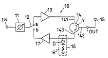
本発明の実施形態について、アクティブフェーズドアレーアンテナに使用する場合を例にとり図1を参照して説明する。
【0028】
入力端子INを通して送信信号が送受信モジュール10に入力する。送信信号は移相器11によって所望位相に設定され、送信側の端子aに接続された送受切り換えスイッチ12を経て電力増幅器13に供給され電力増幅される。その後、送信信号と受信信号とを分離する送受分離回路たとえば非可逆回路素子のサーキュレータ14に加えられる。
【0029】
サーキュレータ14はたとえば第1〜第3の3個の端子141〜143を有し、第1端子141が電力増幅器13に接続し、第2端子142は出力端子OUTおよび放射器15に接続されている。
【0030】
サーキュレータ14に加えられた送信信号は、矢印Yで示した順方向に低損失で通過し、第2端子142から出力端子OUTを経て放射器15に送られ、放射器15から空中に放射される。
【0031】
空中へ放射された送信信号はたとえば目標で反射され、放射器15によって受信される。受信信号は出力端子OUTを経てサーキュレータ14に送られ、矢印Yで示した順方向に低損失で通過し、第3端子143から低反射型リミタ16に送られる。低反射型リミタ16は、たとえばリミタダイオードDと、一端が接地された抵抗R´との直列接続回路で構成されている。
【0032】
受信信号は低反射型リミタ16から低雑音増幅器17に送られ低雑音増幅される。その後、受信側の端子bに接続された送受切り換えスイッチ12および移相器11を経て信号処理回路(図示せず)に送られる。
【0033】
アクティブフェーズドアレーアンテナでは、送受信モジュール10および放射器15の組み合わせが多数設けられ、それぞれの放射器15から放射された送信信号は空間で合成され、所望の放射パターンを形成する。
【0034】
上記した構成によれば、低雑音増幅器17の入力側、たとえば受信信号が伝送する低雑音増幅器17およびサーキュレータ14間に、低反射型リミタ16が接続されている。この場合、放射器15に不要反射成分が受信されると、不要反射成分は低反射型リミタ16で電力振幅が制限される。その結果、低反射型リミタ16を漏れ出て受信信号用の低雑音増幅器17に入力する電力振幅が小さくなり、低雑音増幅器17が保護される。
【0035】
また、低反射型リミタ16は、たとえばリミタダイオードDと抵抗R´との直列接続回路で構成されている。この場合、大電力の不要反射成分が入力し、リミタダイオードDがON状態になると、受信信号が伝送する伝送路は抵抗R´を介して接地される。このとき、不要反射成分の一部は抵抗R´を通して流れる。したがって、低反射型リミタ16は入力する信号をすべて反射する完全反射ではなく、その一部を反射する。つまり、リミタダイオードだけが単独に接続され抵抗が接続されていない場合に比べ、反射成分が小さい低反射になる。
【0036】
この場合、低雑音増幅器17側に漏れ出ないその残りの不要反射成分は、低反射型リミタ16で反射される電力成分Aと、抵抗R´によって熱に変換される電力成分Bとに分かれる。
【0037】
電力成分Aと電力成分Bの和はエネルギー保存則によって一定で、電力成分Aがサーキュレータ14を経て電力増幅器13の出力側に入力する。しかし、電力増幅器13の出力側に入力する電力成分Aは、従来技術の図6や図7で示したようにゼロである必要はなく、電力成分Aをたとえば送信電力の1/10程度に抑えれば、所望の性能が得られ問題は生じない。
【0038】
電力成分Bはその値が小さいほど低反射型リミタの挿入損失が小さくなり、受信系統の雑音特性が良好となる。したがって、電力成分Aと電力成分Bのバランスを最適化し、たとえば電力成分Aを、電力増幅器13が所望の性能を発揮できる範囲の最大値とし、電力成分Bをできるだけ小さくすれば、受信系統および送信系統の各増幅器17、13が保護され、同時に、受信系統における雑音特性の劣化が防止される。
【0039】
上記した構成によれば、低反射型リミタ16を動作させる駆動電力が不要であるため、消費電力はゼロとなる。また、保護回路用のスイッチおよびそれを駆動し、あるいは制御する回路を必要としないため小型化する。また、上記した構成の低反射型リミタ16はMMICに容易に組み込めるため、コストが軽減し、小型化し軽量化した送受信モジュールが実現される。
【0040】
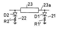
図1では、低反射型リミタは1組のリミタダイオードDと抵抗R´とで構成されている。しかし、図2に示すように、たとえばリミタダイオードD1と抵抗R1´、および、リミタダイオードD2と抵抗R2´が、それぞれ直列に接続された第1および第2の直列接続回路21、22を設け、第1直列接続回路21と第2直列接続回路22との間におよそ1/4波長線路23を接続する構成にすることもできる。
【0041】
この場合、およそ1/4波長線路23の入力端23aにおいて、入力端23aで反射された不要反射成分と、第2直列接続回路22で反射された不要反射成分とが逆相で打ち消し合い、低反射型リミタ16からサーキュレータ14方向に向う不要反射成分を小さくできる。
【0042】
また、リミタダイオードと抵抗が直列に接続された3組以上の直列接続回路を設け、各組の直列接続回路間におよそ1/4波長線路を接続する構成にすることもできる。
【0043】
次に、本発明の他の実施形態について図3を参照して説明する。図3は、図1に対応する部分に同じ符号を付し重複する説明を一部省略する。
【0044】
この実施形態は、低反射型リミタ16が第1方向性結合器31などから構成されている。第1方向性結合器31は、たとえば第1〜第4の4個の端子311〜314を有し、第1端子311から入力した信号が第3端子313および第4端子314に等分され、90°の位相差で出力する構成になっている。
【0045】
第1方向性結合器31は、その第1端子311がサーキュレータ14の第3端子143に接続され、第2端子312に終端抵抗R3が接続され、第3端子313に第1リミタダイオードD3が接続され、第4端子314に第2リミタダイオードD4が接続されている。
【0046】
第1リミタダイオードD3は第2方向性結合器32の第1端子321に接続され、第2リミタダイオードD4は第2方向性結合器32の第2端子322に接続されている。第2方向性結合器32の第3端子323は低雑音増幅器17に接続され、第4端子324は終端抵抗R4に接続されている。第2方向性結合器32は、第1方向性結合器31と同様、第1端子321から入力した信号が第3端子323および第4端子324に等分され、90°の位相差で出力する構成になっている。
【0047】
上記した構成の場合、受信信号は第1方向性結合器31の第3端子313および第4端子314に2分して出力される。それぞれの出力は第1、第2のリミタダイオードD3、D4を経て、第2方向性結合器32の第3端子323に合成されて出力し、受信信号用の低雑音増幅器17で電力増幅される。
【0048】
上記した構成において、第1方向性結合器31の第1端子311に不要反射成分が入力すると、不要反射成分は、第3端子313および第4端子314に出力し、第1および第2のリミタダイオードD3、D4で電力振幅が制限される。したがって、低反射型リミタ16を漏れ出て低雑音増幅器17へ入力する電力振幅は小さくなり、低雑音増幅器17が保護される。
【0049】
この場合、低反射型リミタ16から低雑音増幅器17側へ漏れ出ない残りのほとんどの不要反射成分は、第1および第2のリミタダイオードD3、D4で反射される。しかし、この反射成分は第1方向性結合器31に接続された終端抵抗R3で熱に変換される。その結果、低反射型リミタ16からサーキュレータ14方向に向う不要反射成分はほぼゼロの低反射となり、電力増幅器13の出力側に入力する不要反射成分も抑制される。
【0050】
したがって、図1の構成と同様の効果、たとえば受信信号用の低雑音増幅器17および送信信号用の電力増幅器13を保護するなどの効果が得られる。
【0051】
この場合、図1の構成に比べると、方向性結合器が接続された分だけ損失が増加し、受信系統の雑音特性が劣化する。しかし、その雑音特性は従来技術よりは劣化しない。
【0052】
次に、本発明の他の実施形態について図4を参照して説明する。図4は、図3に対応する部分に同じ符号を付し重複する説明を一部省略する。
【0053】
この実施形態は、第1および第2のリミタダイオードD3およびD4に、それぞれ受信信号用の低雑音増幅器41、42が接続され、一方の低雑音増幅器41は第2方向性結合器32の第1端子321に接続され、他方の低雑音増幅器42は第2方向性結合器32の第2端子322に接続されている。そして、第2方向性結合器32の第3端子が送受切り換えスイッチ12に接続され、第4端子に終端抵抗R4が接続されている。
【0054】
この構成の場合、低雑音増幅器41、42で増幅された受信信号は、第2方向性結合器32の第3端子に合成されて出力される。
【0055】
また、不要反射成分は第1および第2のリミタダイオードD3、D4で電力振幅が制限される。したがって、第1および第2のリミタダイオードD3、D4を漏れ出て低雑音増幅器41、42へ入力する電力振幅が抑えられ、低雑音増幅器41、42が保護される。
【0056】
また、低雑音増幅器41、42へ漏れ出ない残りのほとんどの不要反射成分は、第1および第2のリミタダイオードD3、D4によって反射され、第1方向性結合器31に接続された終端抵抗R3で熱に変換される。したがって、低反射型リミタ16からサーキュレータ14方向に向う不要反射成分はほぼゼロの低反射となり、電力増幅器13の出力側に入力する不要反射成分も抑制される。
【0057】
したがって、図3の構成と同様の効果、たとえば受信信号用の2つの低雑音増幅器41、42、および、送信信号用の電力増幅器13を保護するなどの効果が得られる。
【0058】
上記した構成によれば、低反射型リミタのリミタ機能によって漏れ電力が抑圧され、受信系統の低雑音増幅器が保護される。また、低反射型リミタの低反射機能によって、送信系統に位置する電力増幅器の出力側への入力が軽減し、あるいは抑圧され、送信系統の電力増幅器は所望の性能を安定に発揮できる。
【0059】
また、低反射型リミタにスイッチが用いられないため、回路構成が簡略化し、小型化や低価格化が容易になる。また、低反射型リミタは挿入損失が小さく、受信系統の雑音特性が向上する。また、低反射型リミタは消費電力がなく、MMIC化が容易であるため、安価で小型、軽量なマイクロ波送受信モジュールが容易に得られる。
【0060】
【発明の効果】
本発明によれば、小型化や軽量化が容易な低反射型リミタ並びに低反射型リミタを用いた送受信モジュールおよびアクティブフェーズドアレーアンテナを実現できる。
【図面の簡単な説明】
【図1】本発明の実施形態を説明する回路構成図である。
【図2】 本発明に使用される低反射型リミタの他の例を説明する回路構成図である。
【図3】本発明の他の実施形態を説明する回路構成図である。
【図4】本発明の他の実施形態を説明する回路構成図である。
【図5】従来例を説明する回路構成図である。
【図6】他の従来例を説明する回路構成図である。
【図7】他の従来例を説明する回路構成図である。
【図8】他の従来例を説明する回路構成図である。
【符号の説明】
10…送受信モジュール
11…移相器
12…送受切り換えスイッチ
13…送信側の電力増幅器
14…サーキュレータ
15…放射器
16…低反射型リミタ
17…受信側の低雑音増幅器
IN…入力端子
OUT…出力端子
D…リミタダイオード
R…終端抵抗
R´…抵抗[0001]
BACKGROUND OF THE INVENTION
The present invention relates to a low reflection limiter used for an active phased array antenna and the like, a transmission / reception module using the limiter , and an active phased array antenna .
[0002]
[Prior art]
The transmission / reception module includes an amplifier that amplifies a transmission signal and a reception signal, and is used, for example, for an active phased array antenna. An active phased array antenna has a large number of radiators that radiate transmission signals into space. For example, a transmission / reception module is provided for each radiator. Further, a transmission / reception separating circuit for separating the transmission signal and the reception signal is provided between the radiator and the transmission / reception module. A circuit for connecting such a transmission / reception module and a transmission / reception separation circuit is described in
[0003]
Here, a conventional transmission / reception module will be described with reference to FIG.
[0004]
A transmission signal is input to the transmission /
[0005]
In the active phased array antenna, a large number of combinations of the transmission /
[0006]
For example, if there is an obstacle at a short distance, the transmission signal radiated into the air is reflected by the obstacle and received by the
[0007]
When an unnecessary reflection component having a large power amplitude is directly input to the transmission / reception module, the low-noise amplifier for received signals is deteriorated or destroyed. If an unnecessary reflection component is input to the output side of the power amplifier for transmission signals for some reason, it is equivalent to connecting a load having a poor reflection characteristic to the power amplifier, and desired performance cannot be exhibited.
[0008]
For this reason, in the conventional transmission / reception module, in order to protect the low-noise amplifier for the reception signal and the power amplifier for the transmission signal from unnecessary reflection components, for example, a protection circuit is provided in the reception system that transmits the reception signal.
[0009]
Here, a conventional transceiver module equipped with a protection circuit will be described with reference to FIG. 6, parts corresponding to those in FIG. 5 are denoted by the same reference numerals, and redundant description is partially omitted.
[0010]
In this conventional example, a
[0011]
According to the configuration described above, the signal path of the reception system is blocked by the
[0012]
Next, another example of a conventional transmission / reception module equipped with a protection circuit will be described with reference to FIG. In FIG. 7, parts corresponding to those in FIG.
[0013]
In this conventional example, a 4-
[0014]
In this case, after the unnecessary reflection component passes through the 4-
[0015]
Next, another example of a conventional transmission / reception module equipped with a protection circuit will be described with reference to FIG. In FIG. 8, parts corresponding to those in FIG.
[0016]
In this conventional example, a
[0017]
According to this configuration, during transmission of a transmission signal, the signal path of the reception system is blocked by the
[0018]
Another example of a conventional transmission / reception module is described in
[0019]
[Patent Document 1]
JP-A-9-270601 [0020]
[Problems to be solved by the invention]
In the method of FIG. 6, a PIN diode or a field effect transistor (hereinafter referred to as FET) is usually used as the
[0021]
Since the PIN diode has a small insertion loss, it is possible to obtain a transmission / reception module having a low noise figure and good noise characteristics. However, a drive circuit for turning on / off the PIN diode at a high speed is required, which increases the cost and the size. In addition, power consumption for driving the PIN diode cannot be ignored. In addition, switches using PIN diodes are rarely used as MMICs, and it is difficult to reduce the size by using MMICs.
[0022]
FETs have the advantage of lower power consumption than PIN diodes. In addition, a control circuit for turning on / off the FET at high speed can also be constituted by a CMOS logic circuit or the like, so that the price can be easily reduced. However, a control circuit for turning on / off is required and the size is increased. Further, since the insertion loss is large, the noise characteristic of the receiving system is degraded when the power amplitude of the unnecessary reflection component is increased.
[0023]
The method of FIG. 7 does not require a driving circuit or a control circuit, has an advantage of good noise characteristics and low power consumption. However, since two circulators are used, the cost increases, the size increases, and the mass increases. Therefore, although high performance can be achieved, it is difficult to reduce the size and price of the transmission / reception module.
[0024]
The method of FIG. 8 provides good noise characteristics. However, unnecessary reflected power is input to the power amplifier that amplifies the transmission signal. Therefore, one of the basic functions of the protection circuit, for example, a function for stabilizing the performance of the power amplifier located on the transmission side cannot be obtained. Therefore, the method of FIG. 8 is limited in application when the unnecessary reflection component is small, for example, when the beam scanning angle is narrow. Further, the price, power consumption, size, and the like are the same as those in the configuration of FIG. 6, and further miniaturization is desired.
[0025]
The present invention aims to provide an above-mentioned drawbacks and solves the miniaturization and cost reduction easy low reflective limiter of transceiver module and the transceiver module and the active phased array antenna employing the low reflective limiter To do.
[0026]
[Means for Solving the Problems]
The present invention provides a transmission / reception module comprising a first amplifier for amplifying a transmission signal and a second amplifier for amplifying a reception signal, wherein a low reflection type limiter is provided on the input side of the second amplifier, and the low reflection type limiter is provided . Has a plurality of series connection circuits in which a limiter diode and a resistor are connected in series, and a quarter wavelength line connected between the plurality of series connection circuits .
[0027]
DETAILED DESCRIPTION OF THE INVENTION
The embodiment of the present invention will be described with reference to FIG. 1 by taking as an example the case of use in an active phased array antenna.
[0028]
A transmission signal is input to the transmission /
[0029]
The
[0030]
The transmission signal applied to the circulator 14 passes through the forward direction indicated by the arrow Y with low loss, is transmitted from the
[0031]
The transmitted signal radiated into the air is reflected by the target, for example, and received by the
[0032]
The received signal is sent from the low
[0033]
In the active phased array antenna, a large number of combinations of the transmission /
[0034]
According to the above configuration, the low
[0035]
Further, the low
[0036]
In this case, the remaining unnecessary reflection component that does not leak to the
[0037]
The sum of the power component A and the power component B is constant according to the energy conservation law, and the power component A is input to the output side of the
[0038]
The smaller the value of the power component B, the smaller the insertion loss of the low reflection type limiter, and the better the noise characteristic of the receiving system. Therefore, if the balance between the power component A and the power component B is optimized, for example, the power component A is set to the maximum value within the range in which the
[0039]
According to the above-described configuration, the driving power for operating the low
[0040]
In FIG. 1, the low reflection type limiter is constituted by a set of limiter diodes D and a resistor R ′. However, as shown in FIG. 2, for example, first and second
[0041]
In this case, at the
[0042]
Further, it is possible to provide a configuration in which three or more series connection circuits in which a limiter diode and a resistor are connected in series are provided, and a quarter wavelength line is connected between the series connection circuits of each set.
[0043]
Next, another embodiment of the present invention will be described with reference to FIG. In FIG. 3, parts corresponding to those in FIG.
[0044]
In this embodiment, the low
[0045]
The first
[0046]
The first
[0047]
In the case of the configuration described above, the received signal is divided into two signals and output to the
[0048]
In the configuration described above, when an unnecessary reflection component is input to the
[0049]
In this case, most of the remaining unnecessary reflection components that do not leak from the low
[0050]
Therefore, it is possible to obtain the same effect as the configuration of FIG. 1, for example, the effect of protecting the low-
[0051]
In this case, compared to the configuration of FIG. 1, the loss increases by the amount of connection of the directional coupler, and the noise characteristics of the receiving system are deteriorated. However, the noise characteristics are not deteriorated as compared with the prior art.
[0052]
Next, another embodiment of the present invention will be described with reference to FIG. 4, parts corresponding to those in FIG.
[0053]
In this embodiment, low-
[0054]
In the case of this configuration, the reception signals amplified by the
[0055]
The unnecessary reflection component is limited in power amplitude by the first and second
[0056]
Further, most of the remaining unwanted reflection components that do not leak to the
[0057]
Therefore, an effect similar to that of the configuration of FIG. 3, such as protecting the two
[0058]
According to the above configuration, the leakage power is suppressed by the limiter function of the low reflection type limiter, and the low noise amplifier of the reception system is protected. Further, the low reflection function of the low reflection type limiter reduces or suppresses the input to the output side of the power amplifier located in the transmission system, so that the transmission system power amplifier can stably exhibit desired performance.
[0059]
In addition, since a switch is not used for the low reflection type limiter, the circuit configuration is simplified, and miniaturization and cost reduction are facilitated. Further, the low reflection type limiter has a small insertion loss and improves the noise characteristics of the receiving system. In addition, since the low reflection type limiter does not consume power and can be easily made into an MMIC, an inexpensive, small, and lightweight microwave transmission / reception module can be easily obtained.
[0060]
【The invention's effect】
ADVANTAGE OF THE INVENTION According to this invention, the transmission / reception module and active phased array antenna using the low reflection type limiter which is easy to reduce in size and weight, and a low reflection type limiter are realizable.
[Brief description of the drawings]
FIG. 1 is a circuit configuration diagram illustrating an embodiment of the present invention.
FIG. 2 is a circuit configuration diagram illustrating another example of a low reflection type limiter used in the present invention.
FIG. 3 is a circuit configuration diagram illustrating another embodiment of the present invention.
FIG. 4 is a circuit configuration diagram illustrating another embodiment of the present invention.
FIG. 5 is a circuit configuration diagram illustrating a conventional example.
FIG. 6 is a circuit configuration diagram illustrating another conventional example.
FIG. 7 is a circuit configuration diagram illustrating another conventional example.
FIG. 8 is a circuit configuration diagram illustrating another conventional example.
[Explanation of symbols]
DESCRIPTION OF
Claims (7)
Priority Applications (2)
| Application Number | Priority Date | Filing Date | Title |
|---|---|---|---|
| JP2002318084A JP4141797B2 (en) | 2002-10-31 | 2002-10-31 | Low reflection limiter, transceiver module and active phased array antenna using low reflection limiter |
| US10/695,793 US7151918B2 (en) | 2002-10-31 | 2003-10-30 | Low reflection limiter and transmitting/receiving module utilizing same |
Applications Claiming Priority (1)
| Application Number | Priority Date | Filing Date | Title |
|---|---|---|---|
| JP2002318084A JP4141797B2 (en) | 2002-10-31 | 2002-10-31 | Low reflection limiter, transceiver module and active phased array antenna using low reflection limiter |
Publications (3)
| Publication Number | Publication Date |
|---|---|
| JP2004153653A JP2004153653A (en) | 2004-05-27 |
| JP2004153653A5 JP2004153653A5 (en) | 2005-10-27 |
| JP4141797B2 true JP4141797B2 (en) | 2008-08-27 |
Family
ID=32461308
Family Applications (1)
| Application Number | Title | Priority Date | Filing Date |
|---|---|---|---|
| JP2002318084A Expired - Fee Related JP4141797B2 (en) | 2002-10-31 | 2002-10-31 | Low reflection limiter, transceiver module and active phased array antenna using low reflection limiter |
Country Status (2)
| Country | Link |
|---|---|
| US (1) | US7151918B2 (en) |
| JP (1) | JP4141797B2 (en) |
Families Citing this family (19)
| Publication number | Priority date | Publication date | Assignee | Title |
|---|---|---|---|---|
| KR101031692B1 (en) * | 2002-12-18 | 2011-04-29 | 파나소닉 주식회사 | Radio communication apparatus, radio communication method, antenna apparatus and first duplexer |
| KR100595736B1 (en) | 2004-07-26 | 2006-06-30 | 주식회사 에이텔시스텍 | Design method of low noise amplier in portable internet time division duplexing antenna part and the low noise amplier |
| JP2006311512A (en) * | 2005-03-30 | 2006-11-09 | Toshiba Corp | Transmitter-receiver module and radar equipment with the same |
| JP4509899B2 (en) | 2005-09-07 | 2010-07-21 | 株式会社東芝 | Transceiver module |
| JP4855313B2 (en) * | 2007-03-28 | 2012-01-18 | 三菱電機株式会社 | Amplifier, receiving module, transmitting / receiving module, and antenna device |
| JP4808182B2 (en) | 2007-04-27 | 2011-11-02 | 株式会社エヌ・ティ・ティ・ドコモ | Wireless communication apparatus and power supply method for wireless communication apparatus |
| JP4962298B2 (en) * | 2007-12-19 | 2012-06-27 | 富士通株式会社 | Transceiver |
| JP2009267943A (en) * | 2008-04-28 | 2009-11-12 | Toshiba Corp | Transmission device for railway vehicle and transmission system for railway vehicle |
| JP5300057B2 (en) * | 2009-01-07 | 2013-09-25 | 株式会社ネットコムセック | Transceiver |
| JP5225113B2 (en) * | 2009-01-07 | 2013-07-03 | 三菱電機株式会社 | Communication device |
| CN102668325B (en) * | 2009-10-29 | 2014-12-17 | 日本电业工作株式会社 | Power regeneration apparatus, power regeneration method, power storage system, power storage method, and high-frequency apparatus |
| JP5426434B2 (en) * | 2010-03-05 | 2014-02-26 | 株式会社東芝 | Transceiver module |
| JP5235031B2 (en) * | 2011-03-15 | 2013-07-10 | 島田理化工業株式会社 | Limiter device, radar system |
| JP2013090263A (en) * | 2011-10-21 | 2013-05-13 | Toshiba Corp | Reception circuit for phased array radar and transmission/reception module for phased array radar |
| JP5797313B1 (en) | 2014-08-25 | 2015-10-21 | 株式会社京三製作所 | Regenerative circulator, high frequency power supply device, and high frequency power regeneration method |
| US9871647B2 (en) * | 2014-10-22 | 2018-01-16 | Lg Electronics Inc. | Apparatus and method for cancelling self-interference signal in RF front end |
| KR101557823B1 (en) * | 2014-11-03 | 2015-10-06 | 엘아이지넥스원 주식회사 | Protection circuit for transceiver module |
| JP2019114906A (en) * | 2017-12-22 | 2019-07-11 | ルネサスエレクトロニクス株式会社 | Semiconductor device and semiconductor system |
| CN113162648A (en) * | 2021-03-25 | 2021-07-23 | 中国电子科技集团公司第二十九研究所 | High-power transceiving front-end circuit with active standing wave resistance |
Family Cites Families (5)
| Publication number | Priority date | Publication date | Assignee | Title |
|---|---|---|---|---|
| US3859609A (en) * | 1973-07-23 | 1975-01-07 | Texas Instruments Inc | Absorptive pin attenuators |
| US5896563A (en) * | 1995-04-27 | 1999-04-20 | Murata Manufacturing Co., Ltd. | Transmitting and receiving switch comprising a circulator and an automatic changeover switch which includes an impedance circuit |
| JP3106088B2 (en) * | 1995-05-26 | 2000-11-06 | 三菱電機株式会社 | Radar transponder |
| JPH09270601A (en) | 1996-04-02 | 1997-10-14 | Nec Corp | Transmission reception changeover circuit |
| US6362685B1 (en) * | 2000-07-20 | 2002-03-26 | Rockwell Collins, Inc. | Power amplifier with multilevel power modes |
-
2002
- 2002-10-31 JP JP2002318084A patent/JP4141797B2/en not_active Expired - Fee Related
-
2003
- 2003-10-30 US US10/695,793 patent/US7151918B2/en active Active
Also Published As
| Publication number | Publication date |
|---|---|
| US20040242166A1 (en) | 2004-12-02 |
| US7151918B2 (en) | 2006-12-19 |
| JP2004153653A (en) | 2004-05-27 |
Similar Documents
| Publication | Publication Date | Title |
|---|---|---|
| JP4141797B2 (en) | Low reflection limiter, transceiver module and active phased array antenna using low reflection limiter | |
| US5446464A (en) | Transceiver module | |
| US11711108B2 (en) | Universal transmit/receive module for radar and communications | |
| US4791421A (en) | Transmit-receive module for phased-array antennas | |
| US5027125A (en) | Semi-active phased array antenna | |
| US6362685B1 (en) | Power amplifier with multilevel power modes | |
| JP4962298B2 (en) | Transceiver | |
| US7791536B2 (en) | High power phased array antenna system and method with low power switching | |
| US20070002781A1 (en) | Transmit-receive antenna switch in a TDD wireless communication system | |
| JP2004153653A5 (en) | ||
| US8331388B2 (en) | Circuit arrangement and method of operating a circuit arrangement | |
| KR100840527B1 (en) | Apparatus for transmit/receive antenna switch in tdd wireless communication system | |
| US7436353B2 (en) | Transmitting-receiving module of radar system | |
| US7079815B2 (en) | Monolithic microwave integrated circuit transceiver | |
| EP1630570B1 (en) | Transceiver module for a system of two phased array antennas | |
| JP4594910B2 (en) | Transmission / reception module and phased array radar device | |
| CN113507290B (en) | Bidirectional multi-polarization mode transceiving system and transceiving method thereof | |
| CN112532559A (en) | Numerical control amplitude-phase multifunctional chip and method for transmitting signals in chip | |
| WO2010128330A1 (en) | Radar apparatus | |
| KR101557823B1 (en) | Protection circuit for transceiver module | |
| CN112485764B (en) | Retro-reflector with echo enhancement and phase shift modulation functions | |
| JP5300057B2 (en) | Transceiver | |
| JP3153909B2 (en) | Active phased array antenna | |
| KR200383751Y1 (en) | Non-reflected RF switch composed of balance type | |
| KR20050066524A (en) | Active channel apparatus for active phased array antenna system |
Legal Events
| Date | Code | Title | Description |
|---|---|---|---|
| A521 | Written amendment |
Free format text: JAPANESE INTERMEDIATE CODE: A523 Effective date: 20050711 |
|
| A621 | Written request for application examination |
Free format text: JAPANESE INTERMEDIATE CODE: A621 Effective date: 20050711 |
|
| RD04 | Notification of resignation of power of attorney |
Free format text: JAPANESE INTERMEDIATE CODE: A7424 Effective date: 20050714 |
|
| A977 | Report on retrieval |
Free format text: JAPANESE INTERMEDIATE CODE: A971007 Effective date: 20070921 |
|
| A131 | Notification of reasons for refusal |
Free format text: JAPANESE INTERMEDIATE CODE: A131 Effective date: 20071002 |
|
| A521 | Written amendment |
Free format text: JAPANESE INTERMEDIATE CODE: A523 Effective date: 20071203 |
|
| TRDD | Decision of grant or rejection written | ||
| A01 | Written decision to grant a patent or to grant a registration (utility model) |
Free format text: JAPANESE INTERMEDIATE CODE: A01 Effective date: 20080603 |
|
| A01 | Written decision to grant a patent or to grant a registration (utility model) |
Free format text: JAPANESE INTERMEDIATE CODE: A01 |
|
| A61 | First payment of annual fees (during grant procedure) |
Free format text: JAPANESE INTERMEDIATE CODE: A61 Effective date: 20080611 |
|
| FPAY | Renewal fee payment (event date is renewal date of database) |
Free format text: PAYMENT UNTIL: 20110620 Year of fee payment: 3 |
|
| R151 | Written notification of patent or utility model registration |
Ref document number: 4141797 Country of ref document: JP Free format text: JAPANESE INTERMEDIATE CODE: R151 |
|
| FPAY | Renewal fee payment (event date is renewal date of database) |
Free format text: PAYMENT UNTIL: 20110620 Year of fee payment: 3 |
|
| FPAY | Renewal fee payment (event date is renewal date of database) |
Free format text: PAYMENT UNTIL: 20120620 Year of fee payment: 4 |
|
| FPAY | Renewal fee payment (event date is renewal date of database) |
Free format text: PAYMENT UNTIL: 20120620 Year of fee payment: 4 |
|
| FPAY | Renewal fee payment (event date is renewal date of database) |
Free format text: PAYMENT UNTIL: 20130620 Year of fee payment: 5 |
|
| LAPS | Cancellation because of no payment of annual fees |