JP4139952B2 - COPOLYMER POLYMER FILM, METHOD FOR FORMING THE SAME, AND SEMICONDUCTOR DEVICE USING COPOLYMER POLYMER FILM - Google Patents
COPOLYMER POLYMER FILM, METHOD FOR FORMING THE SAME, AND SEMICONDUCTOR DEVICE USING COPOLYMER POLYMER FILM Download PDFInfo
- Publication number
- JP4139952B2 JP4139952B2 JP2002223960A JP2002223960A JP4139952B2 JP 4139952 B2 JP4139952 B2 JP 4139952B2 JP 2002223960 A JP2002223960 A JP 2002223960A JP 2002223960 A JP2002223960 A JP 2002223960A JP 4139952 B2 JP4139952 B2 JP 4139952B2
- Authority
- JP
- Japan
- Prior art keywords
- organic monomer
- polymer film
- organic
- monomer
- film
- Prior art date
- Legal status (The legal status is an assumption and is not a legal conclusion. Google has not performed a legal analysis and makes no representation as to the accuracy of the status listed.)
- Expired - Fee Related
Links
Images


Classifications
-
- H—ELECTRICITY
- H01—ELECTRIC ELEMENTS
- H01L—SEMICONDUCTOR DEVICES NOT COVERED BY CLASS H10
- H01L2924/00—Indexing scheme for arrangements or methods for connecting or disconnecting semiconductor or solid-state bodies as covered by H01L24/00
- H01L2924/0001—Technical content checked by a classifier
- H01L2924/0002—Not covered by any one of groups H01L24/00, H01L24/00 and H01L2224/00
Description
【0001】
【発明の属する技術分野】
本発明は、半導体装置における素子間を結ぶ多層配線間の絶縁に好適な絶縁膜及びその形成方法、その絶縁膜を用いた多層配線構造を有する半導体装置、ならびに高分子膜成長装置に関する。
【0002】
【従来の技術】
半導体集積回路の設計ルールは縮小を続けており、それに伴い、配線幅が減少し、隣接する配線間の間隔も狭くなっている。その結果、配線間の寄生容量に起因する遅延により高速動作性能の劣化が顕在化している。つまり、半導体集積回路において、配線信号遅延は配線CR時定数(C:配線容量、R:配線抵抗)に依存するが、配線幅の減少による配線抵抗の増大および配線間隔の減少による配線間容量の増大により配線CR時定数が大幅に増大すると、トランジスタのスイッチング速度向上に対して配線での信号伝達速度が追従できない状態が懸念されている。従来、半導体集積回路の配線材料にはアルミ合金が主に使用されていたが、より高速な動作が必要な集積回路では配線の低抵抗化のため銅配線が使用されている。
【0003】
一方、配線間容量の増大を回避するために、配線間の絶縁膜として、従来広く利用されているシリカ(SiO2)系絶縁膜よりも、比誘電率の低い絶縁膜材料の採用が進められている。このような比誘電率の低い絶縁膜としては、フッ素添加シリカ(SiOF)膜やポーラスシリカ膜、有機高分子膜(有機絶縁膜)が知られている。
【0004】
フッ素添加シリカの成膜方法としては、例えば特開2002−16061号公報(以後「引例1」と表記)に、ヘキサメチルジシロキサンなどの有機シリコン化合物と炭素2重結合を2つ以上有するフッ化炭素化合物との混合ガスをプラズマ重合反応させてフッ化炭素含有シリコン酸化膜を形成する方法が記載されている。かかる重合反応では、重合生成物として環状炭化水素が形成される反応経路は含まれないことから、有機シリコン化合物とフッ化炭素化合物とが強固な環状炭化水素を介して接続されることはない。このため、十分な機械強度が得られない。
【0005】
フッ素添加シリカは、現在、既に一部の市販製品で使用されているものの、膜自身の低誘電率化を図るために膜中のフッ素濃度を高くすると、水分あるいは水素との反応によって生じるフッ化水素で配線金属の腐食が発生したり、フッ素が脱離することにより比誘電率が増大するといった課題が生じる。加えて、半導体集積回路技術の進歩により、絶縁膜への低誘電率化の要求は、既にフッ素添加シリカ(SiOF)膜で得られる3.3程度の比誘電率では十分に応えられなくなってきている。すなわち、比誘電率が3以下と非常に小さな絶縁材料が注目されている。
【0006】
例えば、特開平11−288931号公報(以後「引例2」と表記)には、シロキサン(-Si-O-Si-)に飽和炭化水素基が結合したシリコン系炭化水素化合物の気化ガスを用いたプラズマ重合技術で、比誘電率3以下のシリコン系有機絶縁膜が得られることが記載されている。この場合、飽和炭化水素基自体は安定であるためプラズマ中の電子エネルギーで飽和炭化水素基の構成分子の一部を解離させて活性化させている。かかる重合反応においても、環状炭化水素が形成される反応経路は含まないことから、シリコン系炭化水素化合物同士が強固な環状炭化水素を介して接続されることはない。このため、十分な機械強度が得られず、さらに、シリコン系有機絶縁膜に微細な空孔を導入するポーラス膜の分子設計も困難である。
【0007】
特表2002−503879号公報(以後「引例3」と表記)には、特定範囲のRFパワーレベルのプラズマ処理により、解離させた酸化ガスと、炭化水素基とシロキサン又はシランとからなるオルガノシリコン化合物とを反応させて低誘電率膜を堆積処理する方法が記載されている。この反応過程においても、環状炭化水素が形成される反応経路は含まれないことから、オルガノシリコン化合物が強固な環状炭化水素を介して接続されることはなく、このため、十分な機械強度が得られない。また、プラズマ中でオルガノシリコン化合物を酸化させる際、その酸化反応や酸化度を制御することが難しい。さらには、シリコン系有機絶縁膜に微細な空孔を導入するポーラス膜の分子設計も困難である。
【0008】
一方で、現在、半導体集積回路上の多層配線間を絶縁するシリカ系以外の層間絶縁膜として、耐熱性・耐吸湿性に優れた有機高分子膜の開発が急がれている。
【0009】
有機高分子膜の耐湿性を高めるには、有機モノマー中に親水基が含まれないことが肝要である。また、その有機高分子膜の骨格を形成する有機モノマーの重合反応は水分子を生成させる縮重合反応を経由しないことが望ましいとされている。ここで有機モノマーとは、かかる有機モノマーを構成単位として、重合反応を生じ、目的とする有機高分子(有機ポリマー)を形成する原料化合物を指す。
【0010】
層間絶縁膜としての機能性を有する有機高分子膜の成膜方法としては、有機高分子膜の成膜に広く用いられているスピンコーティング法がある。このスピンコーティング法は、溶媒に溶解した有機モノマーを塗布して被膜を形成した後、溶媒を除去するとともに、加熱により有機モノマーの重合反応を進行させ、この結果、2次元あるいは3次元の網目構造をもった高分子膜が形成される。得られた高分子膜からなる有機絶縁膜を構成する骨格は、有機溶剤にとけていた有機モノマーの構造によってきまる。
【0011】
例えば、“REAL-TIME FT-IR STUDIES OF THE REACTION KINETICS FOR THE POLYMERIZATION OF DIVINYL SILOXANE BIS BENZOCYCLO BUTENE MONOMERS”,Material Research Symposium Proceeding,Vol.227,p.103, 1991,T.M.Stokich, Jr., W.M.Lee, R.A.Peters (以後「引例4」と表記)には、ジビニルシロキサンビスベンゾシクロブテンモノマーをメシチレンに溶解させた溶液をスピン塗布した後、100℃でベークして溶媒であるメシチレンを除去し、その後、さらに300℃〜350℃まで加熱すると、ベンゾシクロブテン骨格中の炭素四員環の熱開環重合反応で、下記化学式に示す、ジビニルシロキサンビスベンゾシクロブテンを骨格とした3次元分子鎖からなる有機高分子膜が形成される記述がある。
【0012】
ジビニルシロキサンビスベンゾシクロブテンモノマー(DVS−BCBモノマー)
【0013】
【化4】
【0014】
【化5】
【0015】
また、スピンコーティング法は、塗布膜をベーク炉中で加熱して、まず溶剤を除去した後、さらに高温で加熱して有機モノマーの重合反応を起こして有機高分子膜を形成するものである。すなわち、基本的に、熱エネルギーを利用して重合反応を起こしているため、例えば400℃、30分といった高温・長時間の熱処理を必要とする。最近のULSIデバイスでは、多層化がより一層進められ、例えば9層近くの多層配線を形成する場合もあり、多層化が進行すると、スピン塗布膜の高温ベーク累積時間が増大するため、銅多層配線の信頼性が低下しやすくなる。さらに、ベーク炉中に酸素が存在すると、酸素と有機モノマーの一部が反応して目的とする有機高分子膜が形成されない場合もある。そのため、ベーク炉全体を窒素ガス置換する必要があり、これは低コスト化の阻害要因の一つとなる。
【0016】
また、スピンコーティング法は、その塗布処理を、局所排気されたスピン塗布室で行うが、その際、浮遊している粉塵粒子や、スピン塗布室の内壁にこびりつき乾燥、固化した有機モノマーの微粒子などが、形成されるスピン塗布膜に混入して、膜質を劣化させる場合もある。さらに、スピン塗布では、大量の有機溶剤を必要とし、環境負荷が大きいといった課題もある。加えて、下地膜と形成された有機高分子膜との密着性不足の課題も指摘されている。
【0017】
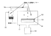
本発明者は、特開平11−17006号公報(特願平09−164688、以下「引例5」と表記)にて、有機モノマーを気化させ、気相からモノマー分子を供給し、基板上で熱重合を行って有機高分子膜を得る方法を提案している。図6に、この方法に用いられる成膜装置を示す。タンク55中の有機モノマーを減圧下で加熱して蒸発させる。一方、反応室を排気ポンプ50により減圧し、気化原料配管56を通して蒸発した有機モノマーを反応室51に送る。有機モノマー分子は、半導体集積回路が形成された半導体基板53の表面に吸着される。その際、半導体基板53は、基板加熱部54によって加熱されており、この熱エネルギーによって重合反応が進行し、架橋構造を有する有機絶縁膜52が形成される。この方法は、スピンコーティング法と異なり、有機溶剤を利用せず、また減圧反応室で成膜するため、酸素が存在しない雰囲気で成膜することができる。したがって、スピンコーティングにおいて生じる酸素との反応や、被膜中に残留する溶媒の気化に伴うボイドの発生など、膜質の低下要因を原理的に有していない点で優れていた。しかしながら、重合反応速度を増大させるため基板温度を上げると、一旦吸着した有機モノマー分子の離脱速度が増し、基板上への実効的な吸着速度が減少し、結果的に所望の成膜速度が得られないといった技術課題を有していた。
【0018】
【発明が解決しようとする課題】
本発明者は、特開2000−12532号公報(特願平10−170016、以下「引例6」と表記)において、機能性有機高分子膜の成膜方法としてMVP(Monomer-Vapor Polymerization)法を提案している。この方法は、有機高分子膜の骨格を形成する有機モノマーを気化させ、キャリアガスを用いて気相中を輸送し、反応室中に形成されたHeプラズマを介して加熱基板表面に吹き付けることで、基板表面に有機高分子膜を形成するものである。気相輸送された有機モノマーは、プラズマ環境を通過する際に励起され、より反応性を増した状態となって基板表面に到達し、重合反応を起こす。予め励起された有機モノマー分子は、比較的わずかな熱エネルギーを加えるだけで容易に重合反応を起こすため、基板温度をそれほど高くしなくても所望の重合速度を達成できる。また、出発原料の化学構造と全く異なる構造を有する膜が形成されるCVD法に対して、MVP法は、出発原料の化学構造を骨格とする構造を有する膜が形成されるため、膜厚や膜質を高い再現性で高精度に制御することができる利点を有している
具体的には、前記のDVS−BCBモノマーガスをプラズマ中で活性化させて、DVS−BCBモノマー中のシクロブテン構造と、別のDVS−BCBモノマー中の二重結合とを付加重合させてDVS−BCB高分子膜を得た。ここで、付加重合は下記の式で示されるように、シクロブテン構造と二重結合との付加反応により炭化水素6員環が形成され、この炭化水素6員環を介してモノマーが結合される。なお、このMVP法は、従来のプラズマCVD法あるいはプラズマ重合法と区別するため、プラズマ付加重合法と呼ぶ。
【0019】
ベンゾシクロブテン構造の開環反応
【0020】
【化6】
【0021】
【化7】
【0022】
そこで、さらに低い誘電率を達成するためには、得られる有機高分子膜の嵩密度を小さくすることが有効な手段であり、そのためには有機高分子膜にその嵩密度を小さくできる有機骨格を導入する必要がある。しかし、このような手段には、嵩密度を小さくすることによる低誘電率化と、他の半導体材料との高い密着性との両立が困難であるという問題がある。有機高分子膜の比誘電率は小さいものの、より低誘電率化を図るためには、酸素やシリコンといった極性元素をなるべく少なくすることが必要である。しかしながら、これらの極性元素の存在により他の半導体材料との密着性が向上する。このように、有機高分子膜の低誘電率化と密着性とはトレードオフの関係にある。
【0023】
このような問題を解決するためには、理想的には、他の半導体材料と接して界面を形成する表面、すなわち有機高分子膜の上面層および底面層(下面層)のみが他の半導体材料との密着性に優れる材料から構成されていることが望ましいといえる。
【0024】
DVS−BCBモノマーといった単一のモノマー原料を用いた従来のプラズマ付加重合法においては、成膜条件の変化、例えばプラズマ生成のRFパワーや成長圧力によるある程度の構造変化は可能であったが、界面付近の比誘電率や密着性を精度よく制御することは困難であった。つまり、従来のプラズマ付加重合法においては、膜厚方向の連続的かつ大幅な膜質制御は実質的に不可能であった。
【0025】
本発明は、以上のような問題に鑑みてなされたものであって、低誘電率でありながら密着性にも優れる有機高分子膜、およびこれを用いた多層配線構造を有する半導体装置を提供することを目的とするものである。また、このような有機高分子膜を気相成長により形成する成膜方法、およびその成膜方法に好適な高分子膜成長装置を提供することを目的とするものである。
【0026】
【課題を解決するための手段】
本発明は、上記の目的を達成するために鋭意検討した結果、特定の複数種の有機モノマーに由来する骨格を含む共重合高分子膜によれば、低誘電率で且つ密着性に優れる絶縁膜を提供し得ることを見出し、本発明を完成するに至った。また、特定の複数種の有機モノマーの混合ガスを用いてプラズマ付加重合を行うことによって、膜厚方向に沿って、その膜組成や化学構造を容易に制御できることを見出し、本発明を完成するに至った。
【0027】
すなわち本発明は、シクロブテン構造を少なくとも2つ以上有し且つ極性分子構造を含む結合を有する第1の有機モノマーのガスと、
二重結合を環内に有し且つ該二重結合と第1の有機モノマーのシクロブテン構造との反応により第1の有機モノマーと第2の有機モノマーとが結合し十字型骨格ユニットを形成する脂環式炭化水素である第2の有機モノマーのガスとを含む混合ガスを、減圧下の反応室内において、該反応室内に設置され加熱された下地面に吹き付けて、該下地面上で第1の有機モノマー分子と第2の有機モノマー分子のプラズマ共重合反応を起こして共重合高分子膜の成長を行うことを特徴とする共重合高分子膜の形成方法に関する。
【0028】
また本発明は、前記混合ガスを、前記反応室内に形成されたプラズマ中を通過させた後に前記下地面に吹き付けることを特徴とする上記の共重合高分子膜の形成方法に関する。
【0029】
また本発明は、第1及び第2の有機モノマーガスを前記反応室に供給するに際して、これら有機モノマーガスの相対供給量を経時的に変化させることで、前記混合ガス中の第1及び第2の有機モノマーの相対含有量比を経時的に変化させて、形成される共重合高分子膜の膜厚方向に、第1及び第2の有機モノマーにそれぞれ由来する骨格ユニットの面内平均組成を変化させることを特徴とする上記の共重合高分子膜の形成方法に関する。
【0030】
また本発明は、第1の有機モノマーが、下記化学式で示されるビスベンゾシクロブテン系化合物である上記の共重合高分子膜の形成方法に関する。
【0031】
【化8】
【0032】
また本発明は、第1の有機モノマーが、下記化学式で示されるシロキサンビスベンゾシクロブテンである上記の共重合高分子膜の形成方法に関する。
【0033】
【化9】
【0034】
また本発明は、第1の有機モノマーが、下記化学式で示されるジビニルシロキサンビスベンゾシクロブテンである上記の共重合高分子膜の形成方法に関する。
【0035】
【化10】
【0036】
また本発明は、第1の有機モノマーは単独で重合可能な化合物であり、該第1の有機モノマーを重合開始から重合終了を通して供給して前記混合ガスに含有させ、第2の有機モノマーは重合途中に供給して前記混合ガスに含有させて重合を行い、
前記下地面との界面を含む下層領域および上面を含む上層領域は、第2の有機モノマーに由来する骨格ユニットを含まず、第1の有機モノマーに由来する骨格ユニットを有し、前記下層領域と上層領域の間の中間領域は、第1の有機モノマーと第2の有機モノマーに由来する骨格ユニットを有する、高分子膜を形成することを特徴とする上記の共重合高分子膜の形成方法に関する。
【0037】
また本発明は、シクロブテン構造を少なくとも2つ以上有し且つ極性分子構造を含む結合を有する第1の有機モノマーと、二重結合を環内に有する脂環式炭化水素である第2の有機モノマーとのプラズマ共重合により形成された共重合体高分子膜であって、
第1の有機モノマーのシクロブテン構造と第2の有機モノマーの二重結合との開環付加反応により生じる炭素6員環を介して第1の有機モノマーと第2の有機モノマーとが結合されてなる十字型骨格ユニットを有することを特徴とする共重合高分子膜に関する。
【0038】
また本発明は、エテン−1,2−ジイル(−C=C−)構造および少なくとも2つ以上のシクロブテン構造を有し且つ極性分子構造を含む結合を有する第1の有機モノマーと、二重結合を環内に有する脂環式炭化水素である第2の有機モノマーとのプラズマ共重合により形成された共重合高分子膜であって、
一方の第1の有機モノマーのシクロブテン構造と他方の第1の有機モノマーのエテン−1,2−ジイル(−C=C−)構造との開環付加反応により生じる炭素6員環を介して第1の有機モノマー同士が結合されてなる骨格をもつ領域と、
第1の有機モノマーのシクロブテン構造と第2の有機モノマーの二重結合との開環付加反応により生じる炭素6員環を介して第1の有機モノマーと第2の有機モノマーとが結合されてなる十字型骨格ユニットをもつ領域とを有する共重合高分子膜に関する。
【0039】
また本発明は、第1の有機モノマーはシロキサン結合(Si−O)を有しており、膜厚方向において、シロキサン結合構造の密度が変化していることを特徴とする上記の共重合高分子膜に関する。
【0040】
また本発明は、膜厚方向において、第2の有機モノマーに由来する骨格ユニットの面内平均含有比率が変化していることを特徴とする上記の共重合高分子膜に関する。
【0041】
また本発明は、第1の有機モノマーはシロキサン結合(Si−O)を有しており、膜厚方向において、シロキサン結合構造の密度と、第2の有機モノマーに由来する骨格ユニットの面内平均含有比率とがいずれも変化していることを特徴とする上記の共重合高分子膜に関する。
【0042】
また本発明は、膜中に含まれるシロキサン結合構造の密度の変化は、下地面に接する共重合高分子膜の下面付近の領域および上面付近の領域に比較して、膜厚方向の中間領域において、前記シロキサン結合構造の密度が相対的に低くなっていることを特徴とする上記の共重合高分子膜に関する。
【0043】
また本発明は、膜中に含まれる第2の有機モノマーに由来する骨格ユニットの面内平均含有比率の変化は、下地面に接する共重合高分子膜の下面付近の領域および上面付近の領域に比較して、膜厚方向の中間領域において、前記骨格ユニットの面内平均含有率が相対的に高くなっていることを特徴とする上記の共重合高分子膜に関する。
【0044】
また本発明は、第1の有機モノマーはシロキサン結合(Si−O)を有し、そのシロキサン結合構造の密度と、第2の有機モノマーに由来する骨格ユニットの面内平均含有比率は、それぞれ膜厚方向において変化しており、
下地面に接する共重合高分子膜の下面付近の領域および上面付近の領域に比較して、膜厚方向の中間領域において、前記シロキサン結合構造の密度が相対的に低く、かつ前記骨格ユニットの面内平均含有率が相対的に高くなっていることを特徴とする上記の共重合高分子膜に関する。
【0045】
また本発明は、シロキサン結合(Si−O)及び少なくとも2つ以上のシクロブテン構造を有する第1の有機モノマーと、二重結合を環内に有する脂環式炭化水素である第2の有機モノマーとのプラズマ共重合により形成された共重合高分子膜であって、第1の有機モノマーのシクロブテン構造と第2の有機モノマーの二重結合との開環付加反応により生じる炭素6員環を介して第1の有機モノマーと第2の有機モノマーとが結合されてなる十字型骨格ユニットを有し、第1の有機モノマーに由来するシロキサン結合構造の密度および第2の有機モノマーに由来する骨格ユニットの面内平均含有比率がそれぞれ膜厚方向において変化しており、下地面に接する共重合高分子膜の下面付近の領域および上面付近の領域に比較して、膜厚方向の中間領域において、前記シロキサン結合構造の密度が相対的に低く、かつ前記骨格ユニットの面内平均含有率が相対的に高くなっている共重合高分子膜と、
前記共重合体高分子膜に、金属配線が埋め込まれてなる配線構造を有する半導体装置に関する。
【0046】
また本発明は、前記金属配線は、膜厚方向において少なくとも前記中間領域から前記上面付近の領域にわたって存在し、その金属配線に接続する金属ビアは、少なくとも前記下面付近の領域に埋め込まれている上記の半導体装置に関する。
【0049】
本発明によれば、絶縁膜の原料として特定の複数の有機モノマーを用いることにより、1種の原料モノマーを用いる場合では得えられなかった機能性を持つ高分子膜を得ることができる。また、成膜工程において原料モノマー供給量の制御を、異なる種類の原料モノマーそれぞれに対して独立に行うことにより、膜厚方向に沿って膜構造の制御が可能となる。すなわち本発明によれば、機械強度や密着性に優れながら、低誘電率の高分子膜を提供できる。また、このような高分子膜を配線間絶縁膜として多層配線構造に適用することにより、信頼性および素子特性に優れる半導体装置を提供することができる。
【0050】
【発明の実施の形態】
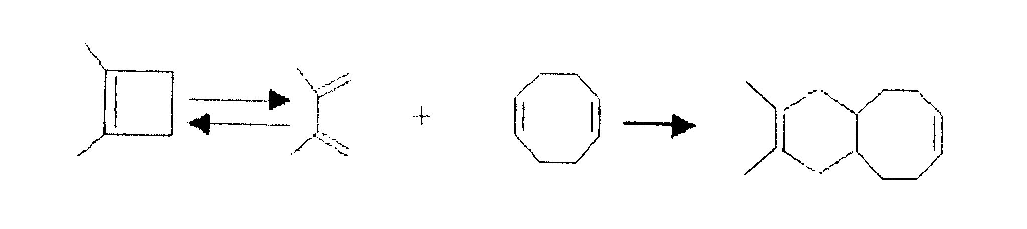
本発明においては、配線間絶縁膜として好適な有機高分子膜を、複数種の有機モノマーを用いたプラズマ付加重合法により形成することができる。このプラズマ付加重合法では、用いる複数の有機モノマーのうち共重合可能な2種類以上の有機モノマーの一方はシクロブテン構造を2つ以上有し、他方の有機モノマーは不飽和結合を2つ以上もつ。また、シクロブテン構造を2つ以上もつ有機モノマーは単独で用いても、その有機モノマー骨格中の不飽和結合が関与する開環・付加重合反応によって高分子膜を形成できることが好ましい。ここでは、共重合可能な2種類以上の有機モノマーが付加重合することで炭化水素環を形成し、この炭化水素環を介して複数の有機モノマーが結合されてゆくことで有機高分子膜を得ることができる。例えば下記化学式に示されるように、一方の有機モノマーが有するシクロブテン構造と、他方の有機モノマーが有する、脂環式炭化水素の環内のエテン−1,2−ジイル(−C=C−)構造(以下適宜「脂環式エテン構造」という)との付加反応を利用することができる。一方の有機モノマーのシクロブテン構造は他方の有機モノマーの環内二重結合との付加反応により炭素6員環を形成し、この炭素6員環を介してモノマー同士が結合される。
【0051】
【化11】
【0052】
【化12】
以下、本発明における有機高分子膜の成膜方法について図1を用いて説明する。ここでは、シクロブテン構造をもつ第1の有機モノマーを「有機モノマーA」、脂環式エテン構造を持つ第2の有機モノマーを「有機モノマーB」と記する。
【0053】
まず、反応室1は、真空ポンプ8により減圧されており、反応室1の内部には基板加熱部6が設けられ、その上に半導体基板5が固定される。原料有機モノマーAおよびBは、それぞれ気化供給システム61、62内において気化され、その蒸気はキャリアガスとともに原料供給配管38A、38B、バルブ18A、18Bを介して反応室1へ供給される。反応室1の壁面はヒータ2により、気化原料供給配管38A、38Bの管壁はヒータ3により加熱され所望の温度に維持されている。有機モノマーAと有機モノマーBの蒸気は、それぞれがキャリアガスとともにシャワーヘッド7へ供給されて混合された後、基板4の表面へ吹き付けられる。その際、シャワーヘッド7と基板加熱部6との間には、RF電源9からRF電力が印加され、プラズマが誘起されている。そのため、有機モノマーAと有機モノマーBの分子はプラズマ雰囲気を通過して励起され、活性化された状態で基板表面に到達する。活性化され基板へ到達した有機モノマーAガスと有機モノマーBガスは、基板加熱部6からの熱エネルギーを受け、速やかに共重合反応を起こし、半導体基板5表面上に共重合高分子絶縁膜4が成長する。
【0054】
なお、未反応の原料は、反応室1が真空ポンプ8により減圧されており、その壁面も保温されていることから、気体状態のまま、ヒータにより加熱されている排気配管16を経て冷却トラップ14へ到達する。冷却トラップ14内では温度が十分に低いため、気体状の原料モノマーA、Bは凝集され、冷却トラップ14内で液化あるいは固化される。その結果、未反応の原料モノマーは、排気ポンプ8には送られることなく、冷却トラップ14内で回収される。
【0055】
図2は、本発明における有機モノマーが液体である場合、あるいは有機溶媒に溶解し溶液として利用する場合に利用可能な、有機モノマー原料の気化供給システムを説明するための模式図である。有機モノマーAタンク23Aから、気化制御器において有機モノマー原料が気化され、反応室へ供給される直前までを示す。なお、以下の説明では単量体である有機モノマーを例に説明するが、二量体である有機オリゴマーでもその原理は同様である。
【0056】
有機モノマーA 22は、バルブ46A、液体流量指示器A 28A、バルブ43Aを介して気化制御器A 30Aに供給される。さらに、有機モノマーA用液体流量指示器28Aからフィードバック制御されている気化制御バルブA 35Aと気化制御機A内バルブ37を介し、気化室A 32Aに供給される。一方、キャリアガスA 26Aはバルブ45Aを経て気化制御器30Aへ供給される。したがって、気化室A 32Aの直前で液体原料モノマーA 22AとキャリアガスA 26Aは混合される。キャリアガスAと混合状態で気化室A 32Aへ供給された液体原料モノマーA 22Aは、気化室32Aへ供給されるときの急激な圧力減少により、同時にヒーター34により受ける熱エネルギーにより連続的に気化する。気化した原料モノマーAは、ヒーターで保温されている原料供給配管38A、バルブ18Aを介して反応室1へ供給される。なお、気化が困難な有機モノマーの場合、有機溶剤にその有機モノマーを溶解し、かかる溶液を気化制御器A 30Aに供給してもよい。
【0057】
図3は、本発明における有機モノマーが固体である場合に利用可能な、有機モノマー原料の気化供給システムを説明するための模式図である。キャリアガス26Bが供給される有機モノマーBタンク23Bから、反応室へ気化された有機モノマー原料が供給される直前までを示す。なお、以下の説明では単量体である有機モノマーを例に説明するが、二量体である有機オリゴマーでもその原理は同様である。
【0058】
キャリアガスB 26Bは気体流量制御器31Bにおいて流量を制御されながら、バルブ45Bを介して有機モノマーBタンク 23Bへ供給される。有機モノマーBタンク 23Bは一定温度に加熱されている。この温度は、有機モノマーBが溶融状態から気化して、あるいは固相状態から昇華して、十分な飽和蒸気圧が得られる温度である。また、気化あるいは昇華状態も温度により制御される。気化したモノマーBは、供給されたキャリアガスと混合され、バルブ46B、気体流量指示器B 33B、バルブ43Bを介して気化原料供給配管38Bへ供給され、さらに、バルブ41Bを介して反応室1へ供給される。その際、単位時間あたりの有機モノマーの供給量は、キャリアガス流量により制御することができる。
【0059】
以上のように、有機モノマー原料が常温で液体であっても固体であっても適切な気化供給システムを選択することで、反応室へ、気体状態の有機モノマーを所定量、供給することができる。なお、常温で気体の有機モノマーを利用する場合は、通常の気体原料ガスやクリーニングガスと同様の供給形態をとればよい。また、本発明において用いられるキャリアガスとしては、ヘリウムガス、アルゴンガス、ネオンガス等の、有機モノマー原料に対して不活性なガスを適宜使用することができる。
【0060】
〔第1の有機モノマー:ベンゾシクロブテン構造を持つ有機モノマー〕
ここでは、第1の有機モノマーの1つとして、ベンゾシクロブテン構造を2つ持つ有機モノマー(以下適宜「ビスベンゾシクロブテン誘導体」という)について具体的に説明する。
【0061】
この有機モノマーは、下記化学式に示すように、ベンゾシクロブテン構造の2つが炭素化合物やシロキサンの二価基Qを介して接続された構造を有する。ベンゾシクロブテン構造は、ベンゼン環とシクロブテン構造をもつ縮合環構造を有し、そのシクロブテン構造は下記化学式に示されるように開環反応を起こす。
【0062】
【化13】
【0063】
エチレン基(−CH2−CH2−)等の炭素数1〜3の直鎖状又は分岐状のアルキレン基;
エテン−1,2−ジイル基(−CH=CH−、ビニレン基)、
1,3−ブタジエン−1,4−ジイル基(−CH=CH−CH=CH−)、
下記化学式に示す2価基
【0064】
【化14】
下記化学式に示すエチン−1,2−ジイル基、
【0065】
【化15】
【0066】
【化16】
等の直鎖状又は分岐状のアルキニレン;
下記化学式に示すフェニレン基、
【0067】
【化17】
【0068】
【化18】
【0069】
【化19】
【0070】
【化20】
【0071】
【化21】
【0072】
【化22】
【0073】
【化23】
【0074】
【化24】
その他の第1の有機モノマーとして、シクロブテン構造を縮合環内に2つ以上有する縮合多環炭化水素構造を有する有機モノマー(以下適宜「縮合多環シクロブテン誘導体」という)について具体的に説明する。例えば、ナフタレン、アントラセン、フェナントレン、ナフタセン、ピレン、クリセンなどの縮合多環炭化水素と2つ以上のシクロブテンとの縮合構造を有するものが挙げられる。さらには、縮合多環炭化水素の一部が飽和炭化水素基あるいは不飽和炭化水素基で置換されたものと2つ以上のシクロブテンとの縮合構造も含まれる。ここで、シクロブテン構造は、第2の有機モノマーと開環付加反応を生じ得るように、他の環と共有しない2つの炭素原子と、他の環と共有し且つ二重結合を形成する二つの炭素原子とから構成される。
【0075】
以下にこのような縮合多環炭化水素構造を有する有機モノマーを例示する。なお、ベンゼン環と2つのベンゾジシクロブテンとが縮合された縮合多環炭化水素構造およびその誘導体も含まれる。
【0076】
【化25】
【0077】
【化26】
【0078】
【化27】
【0079】
【化28】
〔第2の有機モノマー:2つの二重結合を環内に持つ脂環式炭化水素〕
第2の有機モノマーとして用いられる脂環式炭化水素の環内の二重結合は、第1の有機モノマーのシクロブテン構造と付加反応を生じる。
【0080】
具体的には、8員環の脂環式化合物として、シクロオクタテトラエン、1,3,5-シクロオクタトリエン、1,3,6-シクロオクタトリエン、1,4-シクロオクタジエン、1,5-シクロオクタジエン、あるいはそれらに炭化水素基等の置換基が結合されたものが挙げられる。また、6員環の脂環式化合物としては、1,3−シクロヘキサジエン、1,4−シクロヘキサジエン、あるいはそれらに炭化水素基等の置換基が結合されたものが挙げられる。さらに、5員環の脂環式化合物としては、1,3−シクロペンタジエタンあるいはそれに炭化水素基等の置換基が結合されたものが挙げられる。その他、7員環の脂環式化合物として、1,3,5−シクロペプタトリエン、1,3,6−シクロペプタトリエン、1,3−シクロペプタジエンおよびそれらにそれに炭化水素基等の置換基が結合されたものが挙げられる。なお、これらの脂環式炭化水素化合物は、単独で第2の有機モノマーとして使用することもできるし、これらの混合物として使用することもできる。
【0081】
なかでも、下記の脂環式炭化水素が好ましい。
【0082】
【化29】
【化30】
【化31】
【化32】
【化33】
【化34】
【化35】
【化36】
【化37】
ここでは、第1の有機モノマーとしてビスベンゾシクロブテン誘導体と第2の有機モノマーとして1,5-シクロオクタジエン(融点:−56℃)を用いて、プラズマ付加共重合反応を行った場合について説明する。
【0091】
気化されたビスベンゾシクロブテン誘導体はプラズマ中で活性化され、下記化学式に示すように、そのシクロブテン骨格の4員環が開環して2つのビニリデン構造を生じる。
【0092】
【化38】
【0093】
【化39】
【0094】
【化40】
ここでは、第1の有機モノマーとしてビスベンゾシクロブテン誘導体と第2の有機モノマーとして1,3,5-シクロオクタトリエン(融点:−83℃)を用いて、プラズマ付加共重合反応を行った場合について説明する。
【0095】
気化されたビスベンゾシクロブテン誘導体はプラズマ中で活性化され、そのシクロブテン骨格の4員環が開環して2つのビニリデン構造を生じる。
【0096】
一方、気化された1,3,5-シクロオクタトリエンもプラズマ中で活性化され、その環内の一つの二重結合と、ビスベンゾシクロブテン誘導体のシクロブテン骨格が開環して形成された2つのビニリデン構造との付加反応が生じ、形成された炭素6員環を介して、第1の有機モノマーのベンゼン環と第2の有機モノマーの8員環とが接続される。続いて、同様の反応が、第2の有機モノマーの8員環内の他の2つの二重結合のそれぞれと他の第1の有機モノマーとの間でも生じ、結果、下記化学式に示すように、シクロオクタン環に炭素6員環を介して3つのベンゼン環が互いに垂直3方向に結合された骨格ユニットが得られる。
【0097】
【化41】
【0098】
【化42】
ここでは、第1の有機モノマーとしてビスベンゾシクロブテン誘導体と第2の有機モノマーとしてシクロオクタテトラエンを用いて、プラズマ付加共重合反応を行った場合について説明する。
【0099】
気化されたビスベンゾシクロブテン誘導体はプラズマ中で活性化され、そのシクロブテン骨格の4員環が開環して2つのビニリデン構造を生じる。
【0100】
一方、気化されたシクロオクタテトラエンもプラズマ中で活性化され、その環内の一つの二重結合と、ビスベンゾシクロブテン誘導体のシクロブテン骨格が開環して形成された2つのビニリデン構造との付加反応が生じ、形成された炭素6員環を介して、第1の有機モノマーのベンゼン環と第2の有機モノマーの8員環とが接続される。続いて、同様の反応が、第2の有機モノマーの8員環内の他の3つの二重結合のそれぞれと他の第1の有機モノマーとの間でも生じ、結果、下記化学式に示すように、シクロオクタン環にそれぞれ炭素6員環を介して4つのベンゼン環が十字型に結合された骨格ユニットが得られる。
【0101】
【化43】
【0102】
【化44】
ここでは、第1の有機モノマーとして、2つのシクロブテン構造の間に介在する2価基Qがジビニルシロキサン由来の2価基であるビスベンゾシクロブテン誘導体、すなわちDVS−BCBモノマーを用い、第2の有機モノマーとしてシクロオクタテトラエンを用いてプラズマ付加重合反応を行った場合を説明する。
【0103】
この反応においても、前述の実施の形態と同様に第1の有機モノマーのシクロブテン構造と第2の有機モノマーの環内二重結合との開環付加反応により、DVS−BCBモノマーのベンゼン環とシクロオクタテトラエン由来のシクロオクタン環とが炭素6員環を介して接続された骨格ユニットが形成され、この骨格ユニットが格子状に配列した高分子骨格構造が得られる。さらに一方では、DVS−BCBモノマー同士の反応も生じ、一方のモノマーのシクロブテン構造と他方のモノマーの二価基Q内の二重結合とのプラズマ付加重合反応も競合して生じる。その結果、例えば下記化学式に示すように、上記骨格ユニットが格子状に配列された高分子骨格構造において骨格ユニット間を連結する二価基Q内の二重結合とDVS−BCBモノマーのシクロブテン構造との付加反応によって架橋された高強度構造膜が得られる。この架橋密度はDVS−BCBモノマーとシクロオクタテトラエンとの供給量比によって変化させることができる。高分子骨格構造における全ての二価基Qの二重結合を架橋するには、DVS−BCBモノマーの供給量をシクロオクタテトラエン供給量の少なくとも2倍以上とする必要がある。高分子骨格構造内に活性な二重結合が多量に残存すると、膜特性に経時変化が生じるおそれがある。従って、シクロオクタテトラエンの供給量は(あるいは供給速度)は、DVS−BCBモノマーの供給量(あるいは供給速度)に対してモル比で30%以下が好ましく、20%以下がより好ましい。なお、プラズマを利用する成膜方法では、プラズマ中に発生する水素ラジカルと高分子骨格構造内の二重結合との水素付加反応が生じて、架橋後に高分子骨格構造内の二重結合が残存することは極めてまれである。
【0104】
【化45】
ここでは、第1の有機モノマーとして、ナフタレンと2つのシクロブテンとの縮合物である縮合多環シクロブテン誘導体を用い、第2の有機モノマーとしてシクロオクタテトラエンを用いてプラズマ付加共重合反応を行った場合について説明する。
【0105】
気化された縮合多環シクロブテン誘導体はプラズマ中で活性化され、そのシクロブテン骨格の4員環が開環して2つのビニリデン構造を生じる。
【0106】
一方、気化されたシクロオクタテトラエンもプラズマ中で活性化され、その環内の二重結合と、シクロブテン骨格が開環して形成された2つのビニリデン構造との付加反応が生じ、形成された6員環を介して、第1の有機モノマーのナフタレン環と第2の有機モノマーの8員環とが接続される。続いて、同様の反応が第2の有機モノマーの8員環中の他の二重結合と他の第1の有機モノマーとの間でも生じ、結果、下記化学式に示すように、シクロオクタン環に炭素6員環を介して4つのナフタレン環が接続された骨格ユニットが得られる。さらに、この付加反応が複数のベンゾシクロブテン構造部とシクロオクタテトラエンとの間で生じることで、シクロオクタン環に炭素6員環を介して4つのナフタレン環が接続された骨格ユニットがシクロオクタン環を交点として網目格子状に配列した高分子構造が得られる。
【0107】
【化46】
ここでは、第1の有機モノマーとして、ナフタレンと4つのシクロブテンとの縮合物である縮合多環シクロブテン誘導体を用い、第2の有機モノマーとして1,3-シクロヘキサジエンを用いてプラズマ付加共重合反応を行った場合について説明する。
【0108】
気化された縮合多環シクロブテン誘導体はプラズマ中で活性化され、そのシクロブテン骨格の4員環が開環して2つのビニリデン構造を生じる。
【0109】
一方、気化された1,3-シクロヘキサジエンもプラズマ中で活性化され、その環内の二重結合と、シクロブテン骨格が開環して形成された2つのビニリデン構造との付加反応が生じ、形成された6員環を介して、第1の有機モノマーのナフタレン環と第2の有機モノマーの6員環とが接続される。続いて、下記化学式に示すように、同様の反応が第2の有機モノマーの6員環中の他の二重結合と他の第1の有機モノマーとの間でも生じ、結果、炭素6員環に炭素6員環を介して2つのナフタレン環が接続された骨格ユニットが得られる。さらに、この付加反応が、複数のベンゾシクロブテン構造と1,3−シクロヘキサジエンとの間で生じることで、シクロヘキサン環に炭素6員環を介してナフタレン環が接続された骨格ユニットがナフタレン環を交点として網目格子状に配列した高分子構造が得られる。
【0110】
【化47】
【0111】
【実施例】
以下に、第1の有機モノマーとしてDVS−BCBモノマーを用い、第2の有機モノマーとしてシクロオクタテトラエンを用いてプラズマ付加共重合反応を行う場合を例に挙げ、本発明をさらに詳しく説明する。
【0112】
〔共重合高分子膜およびその成膜方法〕
ここで、高分子膜成長装置の有機モノマータンクAにはDVS−BCBモノマーを収容し、有機モノマータンクBにはシクロオクタテトラエンを収容した。キャリアガス26A、26B、パージガスおよび圧力送出ガス27にはいずれもヘリウム(He)を用いた。クリーニングガス21には、NF3と酸素の混合気体、又はSF6と酸素あるいはオゾンの混合気体を用いた。またCF4やC2F6といったフルオロカーボンガスと酸素あるいはオゾンの混合気体でもよい。
【0113】
有機モノマーの気化は次のようにして行った。ここではDVS−BCBモノマーについて説明するが、シクロオクタテトラエンについても同様に行うことができる。
【0114】
まず、高分子膜成長装置(図1)の気化制御器(図2)を初期状態に維持するために、気化制御器内バルブ37A及びバルブ41A、成長装置のバルブ49を「開」とし、真空ポンプ8で、反応室1、排気配管16、廃液配管15、気化制御器38A、気化原料供給配管38Aを真空引きする。
【0115】
有機モノマーの気化温度は、有機モノマーガスの必要供給量を確保するために必要な温度であるとともに、有機モノマーを気相供給する配管過程で分解や重合等による変質および配管の閉塞等を伴わない温度に設定することが望ましい。配管は、成長時に設定される温度に十分に耐えられる耐熱性材料からものを用いることが必要である。また、配管の温度は、配管各所に設置された熱電対によりモニターし、常に設定温度となるよう配管加熱ヒータを制御する。
【0116】
次に、図2に示すバルブ45Aを「開」とし、キャリアガス供給配管40Aからキャリアガス(He)26Aを、気体流量制御器31Aを介して気化制御器30Aに供給し、さらに気化原料供給配管38A、バルブ18Aを介して反応室1に流し、排気配管16を介して真空ポンプ8で装置外に排気する。
【0117】
ここでは、気化温度を210℃とし、Heキャリアガス流量500sccm(500ml/min(normal))とした。この条件の場合、気化制御器の全圧Pは、7Torr(933Pa)であり、反応室1は2.0Torr(267Pa)であった。また、反応室1内に設置された基板加熱部6により、半導体集積回路が形成されたシリコン基板(半導体基板)5を400℃に加熱した。DVS−BCBモノマーとシクロオクタテトラエンを用いた場合の基板加熱温度は200℃〜450℃の範囲内に設定することが好ましい。
【0118】
以上の操作の後、DVS−BCBモノマー及びシクロオクタテトラエンを、それぞれHeキャリアガスとともに、それぞれの気化原料供給配管を介し反応室1へ供給し、混合する。反応室1内へ供給されたこれらのガスは反応室1内のシャワーヘッド7で分散される。シャワーヘッド7には13.56MHzのRFパワーが印加されており、このシャワーヘッド下にHeプラズマを発生させた。RFパワーは100W以下、好ましくは50W以下とし、DVS−BCBモノマー及びシクロオクタテトラエンの付加反応に関与する官能基(シクロブテン構造および二重結合)のみを活性化させることが肝要である。
【0119】
DVS−BCBモノマーとシクロオクタテトラエンの混合ガスは、シャワーヘッド7により分散された後、かかるHeプラズマを通して半導体基板5上に吹き付けられる。400℃に加熱された基板表面上では、DVS−BCBモノマーとシクロオクタテトラエンの共重合反応が生じて共重合高分子膜(有機絶縁膜)が形成される。その際、排気配管16には未反応のDVS−BCBモノマーおよびシクロオクタテトラエンを含むガスが流れるが、20℃程度に冷やされた冷却トラップ14にてガス状のDVS−BCBモノマーとシクロオクタテトラエンが液化され、真空ポンプ8には入り込まない。
【0120】
所定量のDVS−BCBモノマー及びシクロオクタテトラエンを反応室1へ気相供給した後、それぞれの供給を停止し、反応室内の半導体基板5を取り出す。
【0121】
成膜工程においてDVS−BCBモノマーガスとシクロオクタテトラエンガスの相対供給量を経時的に変化させることで、膜厚方向にDVS−BCB由来の骨格ユニットとシクロオクタテトラエン由来の骨格ユニットの比率が異なる、すなわち化学構造の異なる共重合高分子膜が得られる。
【0122】
例えば、重量流量換算で流速0.15g/分のDVS−BCBモノマーのみを30秒間供給し、その後DVS−BCBモノマーとシクロオクタテトラエンを同時にそれぞれ流速0.15g/分と0.01g/分で1分間供給した。その後、シクロオクタテトラエンの供給を停止し、流速0.15g/分のDVS−BCBモノマーのみを30秒間供給した。その際、DVS−BCBモノマーは成膜開始から終了まで通して連続的に供給されている。
【0123】
あるいは、成膜開始から終了まで通してDVS−BCBモノマーの供給を重量流量換算で流速0.15g/分で一定とし、シクロオクタテトラエンの供給速度を最初の30秒間で流速0g/分から0.01g/分へ増加させ、その後、流速0.01/分で1分間保ち、次に30秒間で流速0.01g/分から0g/分へ減少させることもできる。この場合、DVS−BCB由来の骨格ユニットとシクロオクタテトラエン由来の骨格ユニットの相対量が膜厚方向に連続的に変化した共重合高分子膜が得られる。
【0124】
図4に、得られる共重合高分子膜の模式的断面図を示す。成膜の初期および終了時期では、DVS−BCBモノマーを含みシクロオクタテトラエンを含まないガス或いはDVS−BCBモノマーの相対含有量の多いガスを供給するため、下地膜およびキャップ膜との界面付近の層領域では、それぞれ中間領域に対してDVS−BCB由来の骨格ユニットが相対的に多い。これにより、下地膜やキャップ膜を構成する他の材料との密着性に優れた共重合高分子膜が得られる。一方、成膜の中間時期では、シクロオクタテトラエンの供給を開始する或いは供給量を増やすため、膜厚方向の中間領域においては相対的にDVS−BCB由来の骨格ユニットは少なく、シクロオクタテトラエン由来の骨格ユニットを比較的多く含んだ共重合高分子膜が得られる。すなわち、共重合高分子膜の中間領域は相対的に嵩密度が小さく低誘電率となる。シクロオクタテトラエン由来の骨格ユニットを比較的多く含んだ共重合膜領域では、膜中に含まれる酸素やシリコンが少ないため、相対的に比誘電率が低くなる。
【0125】
なお、図4では説明のために構造の異なる3層膜のように記載しているがこれらは連続した層である。先に述べたように、有機モノマーの供給量はそれぞれ独立に制御可能であるので、ゆるやかに供給量を変化させる場合は連続的にゆるやかに構造が変化をした共重合高分子膜が得られる。また、急激に供給量を変化させることにより連続的に急激に構造が変化した共重合高分子膜を形成することが可能である。
【0126】
〔多層配線構造およびその形成方法〕
本発明の共重合高分子膜をMOSFETデバイスの多層配線構造に適用した場合について図5を用いて説明する。
【0127】
ここでは、上記の実施例で説明した共重合高分子膜を、シリコン基板81に形成されたMOSFET82上に設けられた3層の銅配線85、87、89(M1、M2、M3)を埋め込むための絶縁膜に適用した。
【0128】
第1の銅配線(M1)85は、MOSFET82上の無機層間絶縁膜84に形成されている銅コンタクトプラグ83上に形成され、配線間絶縁膜91にバリア金属膜を介して埋め込まれている。無機層間絶縁膜84の表面には銅拡散バリアキャップ膜として10nm厚以下の極薄膜シリコン窒化膜90が形成されている。このキャップ膜90上に形成された配線間絶縁膜91は、DVS−BCB由来の骨格ユニットを多く含むDVS−BCB高分子膜91aと、DVS−BCB及びシクロオクタテトラエン由来の骨格ユニットを含むDVS−BCB・シクロオクタテトラエン共重合高分子膜91bと、DVS−BCB由来の骨格ユニットを多く含むDVS−BCB高分子膜91cの連続した3つの層状領域からなる構造を有している。
【0129】
この配線間絶縁膜91において、下地膜および上地膜との界面付近の領域には、機械的強度と密着性に優れたDVS−BCB高分子膜91a、91cを配置している。これらのDVS−BCB高分子膜(比誘電率k=2.5)は、単位骨格あたり2つのシロキサン基を含んでおり、高い機械的強度を有しながら銅拡散バリア膜(タンタル系金属等)との密着性に優れる。
【0130】
配線間絶縁膜91の中間領域を構成するDVS−BCB・シクロオクタテトラエン共重合高分子膜91bは、そのシロキサン濃度がDVS−BCB高分子膜91aの半分以下であり、その比誘電率kは2.1である。
【0131】
第1層目の配線間絶縁膜91の実効誘電率は、DVS−BCB高分子層状領域とDVS−BCB・シクロオクタテトラエン共重合高分子層状領域との厚み比に依存するが、DVS−BCB高分子層状領域の総厚さは、DVS−BCB・シクロオクタテトラエン共重合高分子層状領域の5〜20%程度、例えば10%程度であることが望ましい。例えば、銅配線85の厚さが300nmの場合、DVS−BCB高分子膜91a、DVS−BCB・シクロオクタテトラエン共重合高分子膜91b、DVS−BCB高分子膜91cのそれぞれの厚さは15nm/270nm/15nmとすることができ、この場合の実効比誘電率は2.2〜2.3程度であった。
【0132】
かかる配線間絶縁膜91は、図1に示した共重合高分子膜の成長装置を用いて成長した。ここでは、基板加熱温度を425℃とし、シャワーヘッドには50WのRFパワーを印加してHeプラズマを発生させた。まず、成膜初期ではDVS−BCBモノマーのみを供給して15nm厚のDVS−BCB高分子膜を成長させた。続いて、DVS−BCBモノマーとシクロオクタテトラエンとが等モル供給となるように、例えばDVS−BCBモノマーの流量0.15g/分、シクロオクタテトラエン流量0.01g/分で供給し、270nm厚のDVS−BCB・シクロオクタテトラエン共重合高分子膜を成長した。続いて、再びDVS−BCBモノマーのみを供給して15nm厚のDVS−BCB高分子膜を成長させた。その際、DVS−BCBモノマーは成膜開始から終了まで通して連続的に供給されている。なお、成膜開始から終了まで通してDVS−BCBモノマーの供給量を一定とし、シクロオクタテトラエンの供給量を連続的に増減させれば絶縁膜の全領域がDVS−BCB・シクロオクタテトラエン共重合高分子膜となり、そのシロキサン構造の密度が漸次的に変化し下地膜および上地膜との界面近傍領域で高く中間領域で低くなる膜を形成することもできる。その後、この第1の配線層間絶縁膜91には、配線形成用の溝が形成され、この配線溝内に10nm厚のTaNバリア膜で側面および底面が覆われた第1層目のシングルダマシン銅配線85が形成される。
【0133】
次に、第1の銅配線85上に10nm厚の銅拡散バリアキャップ膜90を成長させ、第2の配線間絶縁膜92を成長する。ここには、第1の銅配線85とビア86と第2の銅配線87からなるデュアルダマシン銅配線が形成される。ここでも、DVS−BCB高分子膜92aとDVS−BCB・シクロオクタテトラエン共重合高分子膜92bとDVS−BCB高分子膜92cの3つの層状領域からなる絶縁膜を成長する。
【0134】
まず、銅ビア86を埋め込む層間絶縁膜領域には機械的強度および密着性に優れるDVS−BCB高分子膜92aを成長する。続いて、DVS−BCB・シクロオクタテトラエン共重合高分子膜92bを成長する。ここでは、DVS−BCBモノマーとシクロオクタテトラエンとのモル供給量比を4:1とし、シロキサン構造の密度をDSV−BCB高分子膜中の75%程度以下とした。DVS−BCB・シクロオクタテトラエン共重合高分子膜92bには、後に配線溝をドライエッチングにより形成するが、その際、下地のDVS−BCB高分子膜92aをエッチング停止層として用いることができる。N2/H2/CFx系エッチングガスを用いた場合、そのエッチング速度は膜中のシロキサン構造の密度に依存する。DVS−BCB・シクロオクタテトラエン共重合高分子膜のシロキサン密度を下地のDVS−BCB高分子膜と比較して75%以下まで小さくしているのは、エッチング選択性を向上させるためである。当然のことながら、その比誘電率は2.0程度となり、配線間容量の低減の観点からも有利である。続いて、このDVS−BCB・シクロオクタテトラエン共重合高分子膜上92bに、機械的強度と密着性に優れたDVS−BCB高分子膜92cを成長する。
【0135】
かかる配線間絶縁膜92も、図1に示した共重合高分子膜の成長装置を用い、DVS−BCBモノマーとシクロオクタテトラエンとの相対供給量を所定量に制御することで連続成長させることができる。
【0136】
この第2の配線間絶縁膜92を構成するDVS−BCB高分子膜92aにはビア孔が開口され、DVS−BCB・シクロオクタテトラエン共重合高分子膜92bとDVS−BCB高分子膜92cには配線溝が形成される。そして、これらの配線溝とビア孔からなる開口部に、その側面と底面をTaNバリア膜で覆われた第2層目のデュアルダマシン銅配線87が形成される。
【0137】
その後、第2の銅配線87上に10nm厚の銅拡散バリアキャップ膜であるSiN膜90を成長させ、第3の配線間絶縁膜93を成長する。ここでは、第2の銅配線87とビア88と第3の銅配線89からなるデュアルダマシン銅配線が形成される。ここでも、ビア88を埋め込む層間絶縁膜領域には機械的強度および密着性に優れるDVS−BCB高分子膜93aを、配線形成部にはDVS−BCB・シクロオクタテトラエン高分子膜93b、その上層には機械的強度および密着性に優れるDVS−BCB高分子膜93cを連続成長する。この成長においては、供給ガスを、有機モノマー成分がDVS−BCBモノマー100%のガスを供給してDVS−BCB高分子膜93aを形成し、続いてDVS−BCBモノマー80モル%、シクロオクタテトラエン20モル%の混合ガスを供給してDVS−BCB・シクロオクタテトラエン高分子膜93bを形成し、そして再びDVS−BCBモノマー100%のガスを供給してDVS−BCB高分子膜93cを形成する。DVS−BCB・シクロオクタテトラエン高分子膜93bの比誘電率は2.2〜1.8程度である。
【0138】
このように、本発明によれば、DVS−BCBモノマーとシクロオクタテトラエンのように、共重合高分子膜を気相反応系において形成可能な2種以上の有機モノマーを用い、その少なくとも一種の有機モノマーが単独で重合可能であることにより、各有機モノマー由来の骨格ユニットの含有量比率を変化させることができる。すなわち、用いる有機モノマーガスの供給比を制御することで各有機モノマー由来の骨格ユニットの含有量比率を膜厚方向に変化させることができ、ULSI多層配線のように各配線層の配線間絶縁膜に対して要求される膜物性、例えば機械強度や密着性、比誘電率を満たすことができる。さらに本発明によれば、高分子膜の嵩密度、言い換えると屈折率が、膜厚方向に連続的あるいはステップ状に変化している有機膜を得ることができる。このような有機高分子膜は光導波路用基板にも用いることができる。
【0139】
以上に説明した高分子膜の成長例では、単独で重合可能な一方の有機モノマーとして、DVS−BCBモノマーを用いたが、本発明では単独でも重合する有機モノマーと、この有機モノマーと共重合可能な他の有機モノマーを含有する混合ガスを用いて共重合高分子膜を気相成長することができれば、これに限定するものではない。なお、本発明の成長方法において、自己重合可能な有機モノマーを含む2種以上の有機モノマーの混合ガスに対して、さらにアセチレンやエチレンといった不飽和鎖式炭化水素等の重合性モノマーを重合補助ガスとして添加して、共重合高分子膜を気相成長させることもできる。
【0140】
【発明の効果】
本発明によれば、特定の有機モノマーガスを複数混合して共重合高分子膜を気相成長することができるため、1種の原料モノマーを用いる場合では得えられなかった機能性を有する高分子膜を得ることが可能となる。さらに、有機モノマーガスの供給量をそれぞれ独立に制御しながら反応室へ供給することで、膜厚方向に沿って膜構造の異なる共重合高分子膜を得ることができる。より具体的には、他の材料層との界面領域に機械強度と密着性に富んだ共重合高分子膜を配置し、その間に位置する中間層に嵩密度の小さな共重合高分子膜を配置することができる。その結果、膜全体として実効比誘電率が低く、かつ密着性および機械的強度に優れた共重合高分子膜を得ることができる。また、このような共重合高分子膜を配線間絶縁膜として多層配線構造に適用することにより、信頼性および素子特性に優れる半導体装置を提供することができる。
【図面の簡単な説明】
【図1】本発明の高分子膜の形成方法の実施に利用可能な成膜装置の概略図である。
【図2】本発明の高分子膜の形成方法に利用される、有機モノマー原料の気化制御器の構成を示す模式図である。
【図3】本発明の高分子膜の形成方法に利用される、有機モノマー原料の気化制御器の構成を示す模式図である。
【図4】本発明の一実施例である共重合高分子膜の断面模式図である。
【図5】本発明の一実施例である共重合高分子膜を用いた多層銅配線構造の断面模式図である。
【図6】有機モノマーを気化させ、気相の有機モノマーを基板上で重合して高分子膜を得る従来法の説明図である。
【符号の説明】
1 反応室
2 反応室加熱ヒータ
3 配管加熱ヒータ
4 共重合高分子膜
5 半導体基板
6 基板加熱部
7 シャワーヘッド
8 真空ポンプ
9 RF電源
10 マッチングボックス
11 RFケーブル
12a、12b アース線
13 気体流量制御器
14 冷却トラップ
15 廃液配管
16 排気配管
17 バルブ
18A、18B バルブ
19A 気化モノマーA
19B 気化モノマーB
20A 排気気化モノマーA
20B 排気気化モノマーB
21 クリーニングガス
22A 有機モノマーA
22B 有機モノマーB
23A 有機モノマーAタンク
23B 有機モノマーBタンク
24A 洗浄溶剤A
25A 洗浄溶剤Aタンク
26A キャリアガスA、
26B キャリアガスB
27 圧力送出ガス
28A 有機モノマーA用液体流量指示器
29A 洗浄溶剤A用液体流量指示器
30A 気化制御器A
31A 気体流量制御器A
31B 気体流量制御器B
32A 気化室
33B 気体流量指示器B
34 ヒータ
35A 気化制御バルブA
36A 洗浄溶剤制御バルブA
37A 気化制御器A内バルブ
38A 気化原料A供給配管
38B 気化原料B供給配管
39A 気化原料A排気配管
39B 気化原料B排気配管
40A キャリアガスA供給配管
40B キャリアガスB供給配管
41A〜48A、41B〜48B バルブ
50 排気ポンプ
51 反応室
52 有機絶縁膜
53 半導体基板
54 基板加熱部
55 タンク
56 気化原料配管
61 気化モノマーA供給システム
62 気化モノマーB供給システム
81 シリコン基板
82 MOSFET
83 銅コンタクトプラグ
84 無機層間絶縁膜
85 第1の銅配線
86 ビア
87 第2の銅配線
88 ビア
89 第3の銅配線
90 銅拡散バリアキャップ膜
91 第1の配線間絶縁膜
91a,c DVS−BCB高分子膜
91b DVS−BCB・シクロオクタトリエン共重合高分子膜
92 第2の配線間絶縁膜
92a,c DVS−BCB高分子膜
92b DVS−BCB・シクロオクタトリエン共重合高分子膜
93 第3の配線間絶縁膜
93a,c DVS−BCB高分子膜
93b DVS−BCB・シクロオクタトリエン共重合高分子膜[0001]
BACKGROUND OF THE INVENTION
The present invention relates to an insulating film suitable for insulation between multilayer wirings connecting elements in a semiconductor device, a method for forming the same, a semiconductor device having a multilayer wiring structure using the insulating film, and a polymer film growth apparatus.
[0002]
[Prior art]
Design rules for semiconductor integrated circuits continue to shrink, and accordingly, the wiring width decreases and the spacing between adjacent wirings also narrows. As a result, the deterioration of the high-speed operation performance becomes obvious due to the delay caused by the parasitic capacitance between the wirings. That is, in the semiconductor integrated circuit, the wiring signal delay depends on the wiring CR time constant (C: wiring capacitance, R: wiring resistance), but the wiring resistance increases due to the reduction in wiring width and the wiring capacitance due to the reduction in wiring spacing. If the wiring CR time constant increases significantly due to the increase, there is a concern that the signal transmission speed in the wiring cannot follow the improvement in the switching speed of the transistor. Conventionally, an aluminum alloy has been mainly used as a wiring material of a semiconductor integrated circuit. However, in an integrated circuit that requires a higher speed operation, a copper wiring is used to reduce the resistance of the wiring.
[0003]
On the other hand, in order to avoid an increase in capacitance between wirings, silica (SiO 2 ) The use of insulating film materials having a lower relative dielectric constant than system insulating films is being promoted. As such an insulating film having a low relative dielectric constant, a fluorine-added silica (SiOF) film, a porous silica film, and an organic polymer film (organic insulating film) are known.
[0004]
As a method for forming a fluorine-added silica film, for example, in Japanese Patent Application Laid-Open No. 2002-16061 (hereinafter referred to as “Reference 1”), a fluoride having two or more carbon double bonds and an organic silicon compound such as hexamethyldisiloxane. A method of forming a fluorocarbon-containing silicon oxide film by plasma polymerization of a mixed gas with a carbon compound is described. In such a polymerization reaction, a reaction path in which a cyclic hydrocarbon is formed as a polymerization product is not included, and therefore the organic silicon compound and the fluorocarbon compound are not connected via a strong cyclic hydrocarbon. For this reason, sufficient mechanical strength cannot be obtained.
[0005]
Fluorine-added silica is currently used in some commercial products, but if the fluorine concentration in the film is increased to reduce the dielectric constant of the film itself, fluorinated silica is generated by reaction with moisture or hydrogen. Problems such as corrosion of the wiring metal due to hydrogen and increase in relative dielectric constant due to desorption of fluorine occur. In addition, due to advances in semiconductor integrated circuit technology, the demand for lower dielectric constants for insulating films cannot be sufficiently met with the specific dielectric constant of about 3.3 already obtained with fluorine-added silica (SiOF) films. Yes. In other words, an insulating material having a relative dielectric constant of 3 or less has attracted attention.
[0006]
For example, in Japanese Patent Laid-Open No. 11-288931 (hereinafter referred to as “Reference 2”), a vaporized gas of a silicon-based hydrocarbon compound in which a saturated hydrocarbon group is bonded to siloxane (—Si—O—Si—) is used. It is described that a silicon-based organic insulating film having a relative dielectric constant of 3 or less can be obtained by a plasma polymerization technique. In this case, since the saturated hydrocarbon group itself is stable, some of the constituent molecules of the saturated hydrocarbon group are dissociated and activated by the electron energy in the plasma. Even in such a polymerization reaction, since a reaction path in which a cyclic hydrocarbon is formed is not included, silicon-based hydrocarbon compounds are not connected to each other through a strong cyclic hydrocarbon. For this reason, sufficient mechanical strength cannot be obtained, and molecular design of a porous film that introduces fine vacancies into the silicon-based organic insulating film is difficult.
[0007]
JP-T-2002-503879 (hereinafter referred to as “Reference 3”) discloses an organosilicon compound comprising an oxidizing gas dissociated by plasma treatment at a specific range of RF power level, a hydrocarbon group, and siloxane or silane. In which a low dielectric constant film is deposited. Even in this reaction process, the reaction route for forming cyclic hydrocarbons is not included, so that the organosilicon compound is not connected via the strong cyclic hydrocarbons, and thus sufficient mechanical strength is obtained. I can't. Moreover, when oxidizing an organosilicon compound in plasma, it is difficult to control the oxidation reaction and the degree of oxidation. Furthermore, it is also difficult to design a porous film that introduces fine pores into the silicon-based organic insulating film.
[0008]
On the other hand, the development of an organic polymer film excellent in heat resistance and moisture absorption as an interlayer insulating film other than a silica-based insulating film that insulates between multilayer wirings on a semiconductor integrated circuit is urgent.
[0009]
In order to improve the moisture resistance of the organic polymer film, it is important that the organic monomer does not contain a hydrophilic group. In addition, it is desirable that the polymerization reaction of the organic monomer forming the skeleton of the organic polymer film does not go through a condensation polymerization reaction that generates water molecules. Here, the organic monomer refers to a raw material compound that causes a polymerization reaction using such an organic monomer as a structural unit to form a target organic polymer (organic polymer).
[0010]
As a method for forming an organic polymer film having functionality as an interlayer insulating film, there is a spin coating method widely used for forming an organic polymer film. In this spin coating method, an organic monomer dissolved in a solvent is applied to form a film, and then the solvent is removed and the polymerization reaction of the organic monomer proceeds by heating. As a result, a two-dimensional or three-dimensional network structure is formed. Thus, a polymer film having the structure is formed. The skeleton constituting the organic insulating film composed of the obtained polymer film is determined by the structure of the organic monomer dissolved in the organic solvent.
[0011]
For example, “REAL-TIME FT-IR STUDIES OF THE REACTION KINETICS FOR THE POLYMERIZATION OF DIVINYL SILOXANE BIS BENZOCYCLO BUTENE MONOMERS”, Material Research Symposium Proceeding, Vol.227, p.103, 1991, TMStokich, Jr., WMLee, RAPeters (Hereinafter referred to as “Reference 4”), a solution of divinylsiloxane bisbenzocyclobutene monomer dissolved in mesitylene was spin-coated and then baked at 100 ° C. to remove mesitylene as a solvent. When heated to ˜350 ° C., an organic polymer film comprising a three-dimensional molecular chain having a skeleton of divinylsiloxane bisbenzocyclobutene represented by the following chemical formula in a thermal ring-opening polymerization reaction of a carbon four-membered ring in the benzocyclobutene skeleton There is a description that is formed.
[0012]
Divinylsiloxane bisbenzocyclobutene monomer (DVS-BCB monomer)
[0013]
[Formula 4]
[0014]
[Chemical formula 5]
[0015]
In the spin coating method, the coating film is heated in a baking furnace to first remove the solvent, and further heated at a high temperature to cause a polymerization reaction of the organic monomer to form an organic polymer film. That is, basically, since a polymerization reaction is caused by using thermal energy, a heat treatment at a high temperature and a long time such as 400 ° C. for 30 minutes is required. In recent ULSI devices, multilayering is further advanced, for example, a multilayer wiring of nearly nine layers may be formed. As the multilayering progresses, the accumulated time of high-temperature baking of the spin coating film increases, so the copper multilayer wiring The reliability of the is likely to be lowered. Further, when oxygen is present in the baking furnace, the target organic polymer film may not be formed due to a reaction between oxygen and a part of the organic monomer. Therefore, it is necessary to replace the entire baking furnace with nitrogen gas, which is one of the factors that hinder cost reduction.
[0016]
In the spin coating method, the coating process is carried out in a locally evacuated spin coating chamber. At that time, floating dust particles, dry, solidified organic monomer particles stuck to the inner wall of the spin coating chamber, etc. However, it may be mixed in the spin coating film to be formed to deteriorate the film quality. Furthermore, spin coating requires a large amount of organic solvent and has a problem that the environmental load is large. In addition, the problem of insufficient adhesion between the base film and the formed organic polymer film has been pointed out.
[0017]
The present inventor disclosed in Japanese Patent Application Laid-Open No. 11-17006 (Japanese Patent Application No. 09-164688, hereinafter referred to as “Reference 5”), vaporized an organic monomer, supplied monomer molecules from the gas phase, and heated on the substrate. A method for obtaining an organic polymer film by polymerization is proposed. FIG. 6 shows a film forming apparatus used in this method. The organic monomer in the
[0018]
[Problems to be solved by the invention]
The present inventor in Japanese Patent Application Laid-Open No. 2000-12532 (Japanese Patent Application No. 10-170016, hereinafter referred to as “Reference 6”) uses an MVP (Monomer-Vapor Polymerization) method as a method for forming a functional organic polymer film. is suggesting. In this method, the organic monomer forming the skeleton of the organic polymer film is vaporized, transported in the gas phase using a carrier gas, and sprayed onto the surface of the heated substrate via He plasma formed in the reaction chamber. An organic polymer film is formed on the substrate surface. The vapor-transported organic monomer is excited when passing through the plasma environment, reaches a substrate surface in a more reactive state, and causes a polymerization reaction. Since the organic monomer molecules excited in advance easily undergo a polymerization reaction by applying a relatively small amount of heat energy, a desired polymerization rate can be achieved without increasing the substrate temperature so much. In contrast to the CVD method in which a film having a completely different structure from the chemical structure of the starting material is formed, the MVP method forms a film having a structure with the chemical structure of the starting material as a skeleton. It has the advantage that the film quality can be controlled with high reproducibility and high accuracy.
Specifically, the DVS-BCB monomer gas is activated in a plasma, and a cyclobutene structure in the DVS-BCB monomer and a double bond in another DVS-BCB monomer are subjected to addition polymerization to form a DVS- A BCB polymer membrane was obtained. Here, in addition polymerization, as shown by the following formula, a hydrocarbon 6-membered ring is formed by an addition reaction between a cyclobutene structure and a double bond, and a monomer is bonded through the hydrocarbon 6-membered ring. This MVP method is called a plasma addition polymerization method in order to distinguish it from the conventional plasma CVD method or plasma polymerization method.
[0019]
Ring-opening reaction of benzocyclobutene structure
[0020]
[Chemical 6]
[0021]
[Chemical 7]
[0022]
Therefore, in order to achieve a lower dielectric constant, it is an effective means to reduce the bulk density of the obtained organic polymer film. For this purpose, an organic skeleton capable of reducing the bulk density is formed on the organic polymer film. It is necessary to introduce. However, such means has a problem that it is difficult to achieve both low dielectric constant by reducing the bulk density and high adhesion to other semiconductor materials. Although the relative permittivity of the organic polymer film is small, it is necessary to reduce polar elements such as oxygen and silicon as much as possible in order to further reduce the permittivity. However, the presence of these polar elements improves the adhesion with other semiconductor materials. Thus, there is a trade-off relationship between lowering the dielectric constant and adhesion of the organic polymer film.
[0023]
In order to solve such a problem, ideally, only the surface forming an interface in contact with another semiconductor material, that is, the upper surface layer and the bottom surface layer (lower surface layer) of the organic polymer film is the other semiconductor material. It can be said that it is desirable to be comprised from the material which is excellent in adhesiveness.
[0024]
In the conventional plasma addition polymerization method using a single monomer raw material such as a DVS-BCB monomer, it is possible to change the film formation conditions, for example, to some extent due to the RF power and growth pressure of plasma generation. It has been difficult to accurately control the relative dielectric constant and adhesion in the vicinity. That is, in the conventional plasma addition polymerization method, continuous and significant film quality control in the film thickness direction has been virtually impossible.
[0025]
The present invention has been made in view of the above problems, and provides an organic polymer film having a low dielectric constant and excellent adhesion, and a semiconductor device having a multilayer wiring structure using the organic polymer film. It is for the purpose. It is another object of the present invention to provide a film forming method for forming such an organic polymer film by vapor phase growth and a polymer film growing apparatus suitable for the film forming method.
[0026]
[Means for Solving the Problems]
As a result of diligent studies to achieve the above object, the present invention provides a low dielectric constant and excellent adhesion film according to a copolymerized polymer film containing a skeleton derived from a plurality of specific organic monomers. The present invention has been completed. In addition, by performing plasma addition polymerization using a mixed gas of a plurality of specific organic monomers, it is found that the film composition and chemical structure can be easily controlled along the film thickness direction, and the present invention is completed. It came.
[0027]
That is, the present invention The Has at least two clobutene structures And having a bond containing a polar molecular structure A gas of a first organic monomer;
Double bond The ring Inside And the reaction between the double bond and the cyclobutene structure of the first organic monomer couples the first organic monomer and the second organic monomer to form a cruciform skeleton unit. A mixed gas containing a gas of the second organic monomer that is an alicyclic hydrocarbon is sprayed on a heated base surface installed in the reaction chamber in a reaction chamber under reduced pressure, and the first base is formed on the base surface. Of the organic monomer molecule and the second organic monomer molecule Plasma The present invention relates to a method for forming a copolymerized polymer film, which comprises causing a polymerization reaction to grow a copolymerized polymer film.
[0028]
The present invention also relates to the above-described method for forming a copolymerized polymer film, wherein the mixed gas is blown onto the base surface after passing through the plasma formed in the reaction chamber.
[0029]
In the present invention, when the first and second organic monomer gases are supplied to the reaction chamber, the relative supply amounts of these organic monomer gases are changed over time, whereby the first and second organic monomer gases in the mixed gas are changed. of By changing the relative content ratio of the organic monomer over time, the in-plane average composition of the skeleton unit derived from the first and second organic monomers is changed in the film thickness direction of the copolymer film to be formed. The present invention relates to a method for forming a copolymer polymer film as described above.
[0030]
The present invention also relates to a method for forming the above-described copolymeric polymer film, wherein the first organic monomer is a bisbenzocyclobutene compound represented by the following chemical formula.
[0031]
[Chemical 8]
[0032]
The present invention also relates to a method for forming the above copolymerized polymer film, wherein the first organic monomer is siloxane bisbenzocyclobutene represented by the following chemical formula.
[0033]
[Chemical 9]
[0034]
The present invention also relates to a method for forming the copolymer polymer film, wherein the first organic monomer is divinylsiloxane bisbenzocyclobutene represented by the following chemical formula.
[0035]
[Chemical Formula 10]
[0036]
In the present invention, the first organic monomer is a compound that can be polymerized alone, and the first organic monomer is supplied from the start of polymerization through the end of polymerization to be contained in the mixed gas, and the second organic monomer is polymerized. It is supplied in the middle and is contained in the mixed gas for polymerization,
The lower layer region including the interface with the base surface and the upper layer region including the upper surface do not include a skeleton unit derived from the second organic monomer, and have a skeleton unit derived from the first organic monomer, The intermediate region between the upper layer regions has a skeleton unit derived from a first organic monomer and a second organic monomer, and forms a polymer film. .
[0037]
The present invention also has at least two cyclobutene structures. And having a bond containing a polar molecular structure First organic monomer and double bond The ring A second organic monomer that is an alicyclic hydrocarbon within Formed by plasma copolymerization of A copolymer polymer film comprising:
The first organic monomer and the second organic monomer are bonded via a carbon 6-membered ring generated by the ring-opening addition reaction between the cyclobutene structure of the first organic monomer and the double bond of the second organic monomer. Cruciform skeleton unit The present invention relates to a copolymerized polymer film characterized by comprising:
[0038]
The present invention also has an ethene-1,2-diyl (—C═C—) structure and at least two cyclobutene structures. And having a bond containing a polar molecular structure First organic monomer and double bond The ring A second organic monomer that is an alicyclic hydrocarbon within Formed by plasma copolymerization of A copolymerized polymer membrane,
The first through the carbon 6-membered ring produced by the ring-opening addition reaction between the cyclobutene structure of one first organic monomer and the ethene-1,2-diyl (—C═C—) structure of the other first organic monomer. A region having a skeleton formed by bonding one organic monomer;
The first organic monomer and the second organic monomer are bonded via a carbon 6-membered ring generated by the ring-opening addition reaction between the cyclobutene structure of the first organic monomer and the double bond of the second organic monomer. Cruciform skeleton unit The present invention relates to a copolymerized polymer film having a region with
[0039]
In the present invention, the first organic monomer has a siloxane bond (Si—O), and the density of the siloxane bond structure is changed in the film thickness direction. Relates to the membrane.
[0040]
The present invention also relates to the copolymer polymer film described above, wherein the in-plane average content ratio of the skeleton unit derived from the second organic monomer is changed in the film thickness direction.
[0041]
In the present invention, the first organic monomer has a siloxane bond (Si—O), and in the film thickness direction, the density of the siloxane bond structure and the in-plane average of the skeleton unit derived from the second organic monomer It is related with said copolymerization polymer film | membrane characterized by all having changed content rate.
[0042]
In the present invention, the density change of the siloxane bond structure contained in the film is observed in the intermediate region in the film thickness direction as compared with the region near the lower surface and the region near the upper surface of the copolymerized polymer film in contact with the base surface. Further, the present invention relates to the above copolymerized polymer film, wherein the density of the siloxane bond structure is relatively low.
[0043]
In the present invention, the change in the in-plane average content ratio of the skeleton unit derived from the second organic monomer contained in the film is changed in the region near the lower surface and the region near the upper surface of the copolymer polymer film in contact with the base surface. In comparison, in the intermediate region in the film thickness direction, the in-plane average content of the skeleton unit is relatively high.
[0044]
In the present invention, the first organic monomer has a siloxane bond (Si-O), and the density of the siloxane bond structure and the in-plane average content ratio of the skeleton unit derived from the second organic monomer are the film Changes in the thickness direction,
Compared to the region near the lower surface and the region near the upper surface of the copolymer polymer film in contact with the lower ground, the density of the siloxane bond structure is relatively low in the middle region in the film thickness direction, and the surface of the skeleton unit It is related with said copolymerization polymer film | membrane characterized by the inner average content rate being comparatively high.
[0045]
The present invention also provides a first organic monomer having a siloxane bond (Si—O) and at least two or more cyclobutene structures, and a double bond. The ring A second organic monomer that is an alicyclic hydrocarbon within Formed by plasma copolymerization of A copolymerized polymer membrane, The first organic monomer and the second organic monomer are bonded via a carbon 6-membered ring generated by the ring-opening addition reaction between the cyclobutene structure of the first organic monomer and the double bond of the second organic monomer. Having a cruciform skeleton unit, The density of the siloxane bond structure derived from the first organic monomer and the in-plane average content ratio of the skeleton unit derived from the second organic monomer are each changed in the film thickness direction, and the copolymerized polymer film in contact with the base surface Compared with the region near the lower surface and the region near the upper surface, the density of the siloxane bond structure is relatively low and the in-plane average content of the skeleton unit is relatively high in the intermediate region in the film thickness direction. Copolymer film made of When ,
In the copolymer polymer film, The present invention relates to a semiconductor device having a wiring structure in which metal wiring is embedded.
[0046]
In the present invention, the metal wiring is present in at least a region near the upper surface from the intermediate region in the film thickness direction, and a metal via connected to the metal wiring is buried in at least the region near the lower surface. The present invention relates to a semiconductor device.
[0049]
According to the present invention, by using a plurality of specific organic monomers as the raw material for the insulating film, a polymer film having functionality that cannot be obtained when one kind of raw material monomer is used can be obtained. In addition, by controlling the supply amount of the raw material monomer independently for each of the different types of raw material monomers in the film formation step, the film structure can be controlled along the film thickness direction. That is, according to the present invention, it is possible to provide a polymer film having a low dielectric constant while being excellent in mechanical strength and adhesion. Further, by applying such a polymer film as an inter-wiring insulating film to a multilayer wiring structure, a semiconductor device having excellent reliability and element characteristics can be provided.
[0050]
DETAILED DESCRIPTION OF THE INVENTION
In the present invention, an organic polymer film suitable as an inter-wiring insulating film can be formed by a plasma addition polymerization method using a plurality of types of organic monomers. In this plasma addition polymerization method, one of two or more types of organic monomers copolymerizable among a plurality of organic monomers to be used has two or more cyclobutene structures, and the other organic monomer has two or more unsaturated bonds. Moreover, it is preferable that even when an organic monomer having two or more cyclobutene structures is used alone, a polymer film can be formed by a ring-opening / addition polymerization reaction involving an unsaturated bond in the organic monomer skeleton. Here, a hydrocarbon ring is formed by addition polymerization of two or more kinds of copolymerizable organic monomers, and an organic polymer film is obtained by bonding a plurality of organic monomers through the hydrocarbon ring. be able to. For example, as shown in the following chemical formula, one organic monomer has a cyclobutene structure, and the other organic monomer has an ethene-1,2-diyl (—C═C—) structure in an alicyclic hydrocarbon ring. (Hereinafter referred to as “alicyclic ethene structure” as appropriate) can be used. The cyclobutene structure of one organic monomer forms a carbon 6-membered ring by an addition reaction with an intracyclic double bond of the other organic monomer, and the monomers are bonded through this carbon 6-membered ring.
[0051]
Embedded image
[0052]
Embedded image
Hereinafter, a method for forming an organic polymer film in the present invention will be described with reference to FIG. Here, the first organic monomer having a cyclobutene structure is referred to as “organic monomer A”, and the second organic monomer having an alicyclic ethene structure is referred to as “organic monomer B”.
[0053]
First, the reaction chamber 1 is depressurized by a vacuum pump 8, a substrate heating unit 6 is provided inside the reaction chamber 1, and a semiconductor substrate 5 is fixed thereon. The raw organic monomers A and B are vaporized in the
[0054]
In addition, since the reaction chamber 1 is decompressed by the vacuum pump 8 and its wall surface is kept warm, the unreacted raw material passes through the
[0055]
FIG. 2 is a schematic diagram for explaining a vaporization supply system of an organic monomer raw material that can be used when the organic monomer in the present invention is a liquid, or when dissolved in an organic solvent and used as a solution. From the organic
[0056]
The organic monomer A 22 is supplied to the vaporization controller A 30A via the
[0057]
FIG. 3 is a schematic diagram for explaining a vaporization supply system of an organic monomer raw material that can be used when the organic monomer in the present invention is a solid. From the organic
[0058]
The
[0059]
As described above, a predetermined amount of gaseous organic monomer can be supplied to the reaction chamber by selecting an appropriate vaporization supply system regardless of whether the organic monomer raw material is liquid or solid at room temperature. . In addition, what is necessary is just to take the supply form similar to normal gaseous source gas and cleaning gas, when using a gaseous organic monomer at normal temperature. In addition, as the carrier gas used in the present invention, a gas inert to the organic monomer raw material such as helium gas, argon gas, neon gas and the like can be appropriately used.
[0060]
[First organic monomer: an organic monomer having a benzocyclobutene structure]
Here, an organic monomer having two benzocyclobutene structures (hereinafter referred to as “bisbenzocyclobutene derivative” as appropriate) will be specifically described as one of the first organic monomers.
[0061]
As shown in the following chemical formula, this organic monomer has a structure in which two benzocyclobutene structures are connected via a divalent group Q of a carbon compound or siloxane. The benzocyclobutene structure has a condensed ring structure having a benzene ring and a cyclobutene structure, and the cyclobutene structure causes a ring-opening reaction as shown in the following chemical formula.
[0062]
Embedded image
[0063]
Ethylene group (-CH 2 -CH 2 A linear or branched alkylene group having 1 to 3 carbon atoms such as-);
Ethene-1,2-diyl group (—CH═CH—, vinylene group),
1,3-butadiene-1,4-diyl group (—CH═CH—CH═CH—),
Divalent group shown in the following chemical formula
[0064]
Embedded image
An ethyne-1,2-diyl group represented by the following chemical formula:
[0065]
Embedded image
[0066]
Embedded image
Linear or branched alkynylene such as
A phenylene group represented by the chemical formula:
[0067]
Embedded image
[0068]
Embedded image
[0069]
Embedded image
[0070]
Embedded image
[0071]
Embedded image
[0072]
Embedded image
[0073]
Embedded image
[0074]
Embedded image
As another first organic monomer, an organic monomer having a condensed polycyclic hydrocarbon structure having two or more cyclobutene structures in the condensed ring (hereinafter referred to as “condensed polycyclic cyclobutene derivative” as appropriate) will be specifically described. Examples thereof include those having a condensed structure of a condensed polycyclic hydrocarbon such as naphthalene, anthracene, phenanthrene, naphthacene, pyrene and chrysene and two or more cyclobutenes. Furthermore, a condensed structure of one in which a part of the condensed polycyclic hydrocarbon is substituted with a saturated hydrocarbon group or an unsaturated hydrocarbon group and two or more cyclobutenes is also included. Here, the cyclobutene structure has two carbon atoms that are not shared with other rings and two that are shared with other rings and form a double bond so that a ring-opening addition reaction can occur with the second organic monomer. Consists of carbon atoms.
[0075]
The organic monomer which has such a condensed polycyclic hydrocarbon structure is illustrated below. A condensed polycyclic hydrocarbon structure in which a benzene ring and two benzodicyclobutenes are condensed and derivatives thereof are also included.
[0076]
Embedded image
[0077]
Embedded image
[0078]
Embedded image
[0079]
Embedded image
[Second organic monomer: alicyclic hydrocarbon having two double bonds in the ring]
The double bond in the ring of the alicyclic hydrocarbon used as the second organic monomer causes an addition reaction with the cyclobutene structure of the first organic monomer.
[0080]
Specifically, as an 8-membered alicyclic compound, cyclooctatetraene, 1,3,5-cyclooctatriene, 1,3,6-cyclooctatriene, 1,4-cyclooctadiene, 1, Examples include 5-cyclooctadiene and those having a substituent such as a hydrocarbon group bonded thereto. Examples of the 6-membered alicyclic compound include 1,3-cyclohexadiene, 1,4-cyclohexadiene, and those obtained by binding a substituent such as a hydrocarbon group thereto. Furthermore, examples of the 5-membered alicyclic compound include those in which 1,3-cyclopentadiethane or a substituent such as a hydrocarbon group is bonded thereto. In addition, as 7-membered alicyclic compounds, 1,3,5-cyclopeptatriene, 1,3,6-cyclopeptatriene, 1,3-cyclopeptadiene and their hydrocarbon groups, etc. In which the substituents are bonded. These alicyclic hydrocarbon compounds can be used alone as the second organic monomer, or can be used as a mixture thereof.
[0081]
Of these, the following alicyclic hydrocarbons are preferred.
[0082]
Embedded image
Embedded image
Embedded image
Embedded image
Embedded image
Embedded image
Embedded image
Embedded image
Embedded image
Here, a case where a plasma addition copolymerization reaction is performed using a bisbenzocyclobutene derivative as the first organic monomer and 1,5-cyclooctadiene (melting point: −56 ° C.) as the second organic monomer will be described. To do.
[0091]
The vaporized bisbenzocyclobutene derivative is activated in plasma, and as shown in the following chemical formula, the 4-membered ring of the cyclobutene skeleton is opened to produce two vinylidene structures.
[0092]
Embedded image
[0093]
Embedded image
[0094]
Embedded image
Here, when a plasma addition copolymerization reaction is performed using a bisbenzocyclobutene derivative as the first organic monomer and 1,3,5-cyclooctatriene (melting point: −83 ° C.) as the second organic monomer Will be described.
[0095]
The vaporized bisbenzocyclobutene derivative is activated in plasma, and the 4-membered ring of the cyclobutene skeleton is opened to produce two vinylidene structures.
[0096]
On the other hand, the vaporized 1,3,5-cyclooctatriene is also activated in the plasma, and is formed by opening one double bond in the ring and the cyclobutene skeleton of the bisbenzocyclobutene derivative. An addition reaction with one vinylidene structure occurs, and the benzene ring of the first organic monomer and the 8-membered ring of the second organic monomer are connected through the formed carbon 6-membered ring. Subsequently, a similar reaction occurs between each of the other two double bonds in the 8-membered ring of the second organic monomer and the other first organic monomer, and as a result, as shown in the following chemical formula: Thus, a skeleton unit in which three benzene rings are bonded to a cyclooctane ring via three carbon atoms in three directions perpendicular to each other is obtained.
[0097]
Embedded image
[0098]
Embedded image
Here, a bisbenzocyclobutene derivative is used as the first organic monomer and a cyclohexane is used as the second organic monomer. Octa A case where a plasma addition copolymerization reaction is performed using tetraene will be described.
[0099]
The vaporized bisbenzocyclobutene derivative is activated in plasma, and the 4-membered ring of the cyclobutene skeleton is opened to produce two vinylidene structures.
[0100]
Meanwhile, vaporized cyclo Octa Tetraene was also activated in the plasma, resulting in an addition reaction between one double bond in the ring and two vinylidene structures formed by the ring opening of the cyclobutene skeleton of the bisbenzocyclobutene derivative. The benzene ring of the first organic monomer and the 8-membered ring of the second organic monomer are connected via the carbon 6-membered ring. Subsequently, a similar reaction occurs between each of the other three double bonds in the 8-membered ring of the second organic monomer and the other first organic monomer, and as a result, as shown in the following chemical formula: Thus, a skeleton unit in which four benzene rings are bonded in a cross shape to a cyclooctane ring via a carbon 6-membered ring is obtained.
[0101]
Embedded image
[0102]
Embedded image
Here, a bisbenzocyclobutene derivative in which a divalent group Q interposed between two cyclobutene structures is a divalent group derived from divinylsiloxane, that is, a DVS-BCB monomer, is used as the first organic monomer, Cycloocta as organic monomer Tetra A case where a plasma addition polymerization reaction is performed using ene will be described.
[0103]
In this reaction as well, the benzene ring of the DVS-BCB monomer and the cyclooctane are added by the ring-opening addition reaction between the cyclobutene structure of the first organic monomer and the intracyclic double bond of the second organic monomer, as in the previous embodiment. Tetra A skeleton unit in which an ene-derived cyclooctane ring is connected via a carbon 6-membered ring is formed, and a polymer skeleton structure in which the skeleton units are arranged in a lattice is obtained. On the other hand, the reaction between DVS-BCB monomers also occurs, and the plasma addition polymerization reaction between the cyclobutene structure of one monomer and the double bond in the divalent group Q of the other monomer also occurs in competition. As a result, for example, as shown in the following chemical formula, in the polymer skeleton structure in which the skeleton units are arranged in a lattice form, a double bond in the divalent group Q connecting the skeleton units and the cyclobutene structure of the DVS-BCB monomer A high-strength structural film crosslinked by the addition reaction is obtained. This crosslink density is determined by DVS-BCB monomer and cycloocta Tetra It can be changed according to the supply amount ratio with the ene. In order to crosslink all the double bonds of the divalent group Q in the polymer skeleton structure, the supply amount of the DVS-BCB monomer is changed to cycloocta Tetra It is necessary to make it at least twice the supply amount of en. If a large amount of active double bonds remain in the polymer skeleton structure, the film characteristics may change with time. Therefore, cycloocta Tetra The supply amount of ene (or supply rate) is preferably 30% or less, more preferably 20% or less, in terms of molar ratio to the supply amount (or supply rate) of the DVS-BCB monomer. In the film formation method using plasma, a hydrogen addition reaction between a hydrogen radical generated in the plasma and a double bond in the polymer skeleton structure occurs, and the double bond in the polymer skeleton structure remains after crosslinking. It is extremely rare to do.
[0104]
Embedded image
Here, a condensed polycyclic cyclobutene derivative that is a condensate of naphthalene and two cyclobutenes is used as the first organic monomer, and cyclohexane is used as the second organic monomer. Octa A case where a plasma addition copolymerization reaction is performed using tetraene will be described.
[0105]
The vaporized condensed polycyclic cyclobutene derivative is activated in plasma, and the 4-membered ring of the cyclobutene skeleton is opened to produce two vinylidene structures.
[0106]
Meanwhile, vaporized cyclo Octa Tetraene is also activated in the plasma, causing an addition reaction between the double bond in the ring and the two vinylidene structures formed by the ring opening of the cyclobutene skeleton, and through the formed 6-membered ring, The naphthalene ring of one organic monomer and the 8-membered ring of the second organic monomer are connected. Subsequently, a similar reaction occurs also between another double bond in the 8-membered ring of the second organic monomer and the other first organic monomer, and as a result, as shown in the following chemical formula, A skeletal unit in which four naphthalene rings are connected via a carbon 6-membered ring is obtained. Furthermore, this addition reaction can be performed with a plurality of benzocyclobutene structures and cyclohexane. Octa Owing to the formation with tetraene, a polymer structure in which a skeleton unit in which four naphthalene rings are connected to a cyclooctane ring via a carbon 6-membered ring is arranged in a mesh lattice pattern with the cyclooctane ring as an intersection is obtained.
[0107]
Embedded image
Here, a condensed polycyclic cyclobutene derivative that is a condensate of naphthalene and four cyclobutenes is used as the first organic monomer, and 1,3-cyclohexadiene is used as the second organic monomer, and the plasma addition copolymerization reaction is performed. The case where it went is demonstrated.
[0108]
The vaporized condensed polycyclic cyclobutene derivative is activated in plasma, and the 4-membered ring of the cyclobutene skeleton is opened to produce two vinylidene structures.
[0109]
On the other hand, the vaporized 1,3-cyclohexadiene is also activated in the plasma, resulting in an addition reaction between the double bond in the ring and the two vinylidene structures formed by opening the cyclobutene skeleton. The naphthalene ring of the first organic monomer and the 6-membered ring of the second organic monomer are connected via the 6-membered ring. Subsequently, as shown in the chemical formula below, a similar reaction occurs between the other double bond in the 6-membered ring of the second organic monomer and the other first organic monomer, resulting in a carbon 6-membered ring. A skeleton unit in which two naphthalene rings are connected to each other through a carbon 6-membered ring is obtained. Furthermore, this addition reaction occurs between a plurality of benzocyclobutene structures and 1,3-cyclohexadiene, so that a skeleton unit in which a naphthalene ring is connected to a cyclohexane ring via a carbon 6-membered ring has a naphthalene ring. A polymer structure arranged in the form of a mesh lattice as intersections is obtained.
[0110]
Embedded image
[0111]
【Example】
In the following, DVS-BCB monomer is used as the first organic monomer, and cycloocta is used as the second organic monomer. Tetra The present invention will be described in more detail by taking as an example a case where a plasma addition copolymerization reaction is carried out using ene.
[0112]
[Copolymer polymer film and film forming method thereof]
Here, the organic monomer tank A of the polymer film growth apparatus contains DVS-BCB monomer, and the organic monomer tank B contains cycloocta Tetra En accommodated. Helium (He) was used for each of the
[0113]
The organic monomer was vaporized as follows. Here, DVS-BCB monomer will be described. Tetra The same can be done for en.
[0114]
First, in order to maintain the vaporization controller (FIG. 2) of the polymer film growth apparatus (FIG. 1) in the initial state, the
[0115]
The vaporization temperature of the organic monomer is a temperature necessary for securing the necessary supply amount of the organic monomer gas, and is not accompanied by deterioration or blockage of the piping due to decomposition or polymerization in the piping process for supplying the organic monomer in the gas phase. It is desirable to set the temperature. The piping must be made of a heat-resistant material that can sufficiently withstand the temperature set during growth. In addition, the temperature of the pipe is monitored by thermocouples installed at various places in the pipe, and the pipe heater is controlled so that the temperature is always set.
[0116]
Next, the
[0117]
Here, the vaporization temperature was 210 ° C., and the He carrier gas flow rate was 500 sccm (500 ml / min (normal)). Under this condition, the total pressure P of the vaporization controller was 7 Torr (933 Pa), and the reaction chamber 1 was 2.0 Torr (267 Pa). Further, the substrate heating unit 6 installed in the reaction chamber 1 heated the silicon substrate (semiconductor substrate) 5 on which the semiconductor integrated circuit was formed to 400 ° C. DVS-BCB monomer and cycloocta Tetra It is preferable to set the substrate heating temperature in the case of using en in the range of 200 ° C to 450 ° C.
[0118]
After the above operation, DVS-BCB monomer and cycloocta Tetra The ene is supplied to the reaction chamber 1 together with the He carrier gas through each vaporized raw material supply pipe and mixed. These gases supplied into the reaction chamber 1 are dispersed by the shower head 7 in the reaction chamber 1. An RF power of 13.56 MHz was applied to the shower head 7, and He plasma was generated under the shower head. The RF power is 100 W or less, preferably 50 W or less, and the DVS-BCB monomer and cycloocta Tetra It is important to activate only the functional groups (cyclobutene structure and double bond) involved in the addition reaction of ene.
[0119]
DVS-BCB monomer and cycloocta Tetra The mixed gas of en is dispersed by the shower head 7 and then sprayed onto the semiconductor substrate 5 through the He plasma. On the substrate surface heated to 400 ° C., DVS-BCB monomer and cycloocta Tetra A copolymerization reaction of ene occurs to form a copolymerized polymer film (organic insulating film). At that time, unreacted DVS-BCB monomer and cycloocta Tetra Gas containing ene flows, but gaseous DVS-BCB monomer and cycloocta are cooled in a
[0120]
A given amount of DVS-BCB monomer and cycloocta Tetra After supplying ethylene to the reaction chamber 1 in a gas phase, the supply of each is stopped, and the semiconductor substrate 5 in the reaction chamber is taken out.
[0121]
DVS-BCB monomer gas and cycloocta Tetra By changing the relative supply amount of Engas over time, DVS-BCB-derived skeletal units and cycloocta Tetra Copolymer polymer films having different ratios of ene-derived skeleton units, that is, different chemical structures can be obtained.
[0122]
For example, only DVS-BCB monomer at a flow rate of 0.15 g / min in terms of weight flow rate is supplied for 30 seconds, and then DVS-BCB monomer and cycloocta Tetra En was simultaneously fed for 1 minute at flow rates of 0.15 g / min and 0.01 g / min, respectively. Then cycloocta Tetra The supply of ene was stopped, and only DVS-BCB monomer at a flow rate of 0.15 g / min was supplied for 30 seconds. At that time, the DVS-BCB monomer is continuously supplied from the start to the end of film formation.
[0123]
Alternatively, the supply of DVS-BCB monomer is kept constant at a flow rate of 0.15 g / min in terms of weight flow rate from the beginning to the end of film formation, Tetra The feed rate of the ene is increased from 0 g / min to 0.01 g / min in the first 30 seconds, then kept for 1 minute at 0.01 / min, and then from 0.01 g / min to 0 g / min in 30 seconds Can also be reduced. In this case, a skeleton unit derived from DVS-BCB and cycloocta Tetra A copolymeric polymer film in which the relative amount of the ene-derived skeleton unit is continuously changed in the film thickness direction is obtained.
[0124]
FIG. 4 shows a schematic cross-sectional view of the obtained copolymer polymer film. At the beginning and end of film formation, DVS-BCB monomer and cycloocta Tetra In order to supply a gas not containing ene or a gas having a large relative content of DVS-BCB monomer, in the layer region near the interface with the base film and the cap film, a skeleton unit derived from DVS-BCB is present in each intermediate region. There are relatively many. Thereby, a copolymerized polymer film excellent in adhesion to other materials constituting the base film and the cap film can be obtained. On the other hand, in the middle of film formation, Tetra In order to start the supply of ene or increase the supply amount, there are relatively few skeleton units derived from DVS-BCB in the middle region in the film thickness direction, and cycloocta Tetra A copolymer polymer film containing a relatively large amount of ene-derived skeleton units can be obtained. That is, the intermediate region of the copolymerized polymer film has a relatively low bulk density and a low dielectric constant. Cycloocta Tetra In the copolymer film region containing a relatively large amount of ene-derived skeleton units, the relative permittivity is relatively low because the film contains less oxygen and silicon.
[0125]
In FIG. 4, for the sake of explanation, a three-layer film having a different structure is shown, but these are continuous layers. As described above, since the supply amount of the organic monomer can be controlled independently, when the supply amount is gradually changed, a copolymer polymer film whose structure is gradually changed continuously can be obtained. Moreover, it is possible to form a copolymerized polymer film whose structure has been changed rapidly and continuously by changing the supply amount rapidly.
[0126]
[Multilayer wiring structure and formation method thereof]
The case where the copolymerized polymer film of the present invention is applied to a multilayer wiring structure of a MOSFET device will be described with reference to FIG.
[0127]
Here, in order to embed the three-layered copper wiring 85, 87, 89 (M1, M2, M3) provided on the
[0128]
The first copper wiring (M1) 85 is formed on the
[0129]
In the inter-wiring insulating
[0130]
DVS-BCB / cycloocta constituting the intermediate region of the inter-wiring insulating
[0131]
The effective dielectric constant of the first-layer inter-wiring insulating
[0132]
The
[0133]
Next, a copper diffusion
[0134]
First, a DVS-
[0135]
The inter-wiring insulating film 92 is also formed using the copolymer polymer film growth apparatus shown in FIG. Tetra Continuous growth can be achieved by controlling the relative supply amount to the predetermined amount.
[0136]
Via holes are opened in the DVS-
[0137]
Thereafter, a
[0138]
Thus, according to the present invention, DVS-BCB monomer and cycloocta Tetra A skeleton derived from each organic monomer by using two or more organic monomers capable of forming a copolymerized polymer film in a gas phase reaction system, such as en, and at least one organic monomer can be polymerized alone. The content ratio of the unit can be changed. That is, by controlling the supply ratio of the organic monomer gas to be used, the content ratio of the skeleton unit derived from each organic monomer can be changed in the film thickness direction, and the inter-wiring insulating film of each wiring layer like a ULSI multilayer wiring Film physical properties required, for example, mechanical strength, adhesion, and dielectric constant can be satisfied. Furthermore, according to the present invention, it is possible to obtain an organic film in which the bulk density of the polymer film, in other words, the refractive index changes continuously or stepwise in the film thickness direction. Such an organic polymer film can also be used for an optical waveguide substrate.
[0139]
In the growth example of the polymer film described above, the DVS-BCB monomer is used as one organic monomer that can be polymerized alone. However, in the present invention, an organic monomer that can be polymerized alone can be copolymerized with the organic monomer. The present invention is not limited to this as long as the copolymerized polymer film can be vapor-phase grown using a mixed gas containing other organic monomers. In the growth method of the present invention, a polymerizable monomer such as an unsaturated chain hydrocarbon such as acetylene or ethylene is further added to the mixed gas of two or more kinds of organic monomers including a self-polymerizable organic monomer. It can also be added as a vapor phase growth of the copolymer polymer film.
[0140]
【The invention's effect】
According to the present invention, the copolymer polymer film can be vapor-grown by mixing a plurality of specific organic monomer gases, and thus has high functionality that could not be obtained when using one kind of raw material monomer. A molecular film can be obtained. Furthermore, by supplying the organic monomer gas to the reaction chamber while independently controlling the supply amount of the organic monomer gas, copolymer polymer films having different film structures along the film thickness direction can be obtained. More specifically, a copolymer polymer film with high mechanical strength and adhesion is placed in the interface region with other material layers, and a copolymer polymer film with a low bulk density is placed in the intermediate layer located between them. can do. As a result, a copolymeric polymer film having a low effective relative dielectric constant as a whole and excellent adhesion and mechanical strength can be obtained. Further, by applying such a copolymerized polymer film as an inter-wiring insulating film to a multilayer wiring structure, a semiconductor device having excellent reliability and element characteristics can be provided.
[Brief description of the drawings]
FIG. 1 is a schematic view of a film forming apparatus that can be used for carrying out a method for forming a polymer film of the present invention.
FIG. 2 is a schematic diagram showing the configuration of an organic monomer raw material vaporization controller used in the polymer film formation method of the present invention.
FIG. 3 is a schematic diagram showing the configuration of an organic monomer raw material vaporization controller used in the polymer film forming method of the present invention.
FIG. 4 is a schematic cross-sectional view of a copolymerized polymer film according to one embodiment of the present invention.
FIG. 5 is a schematic cross-sectional view of a multilayer copper wiring structure using a copolymerized polymer film according to an embodiment of the present invention.
FIG. 6 is an explanatory diagram of a conventional method for obtaining a polymer film by vaporizing an organic monomer and polymerizing the organic monomer in a gas phase on a substrate.
[Explanation of symbols]
1 reaction chamber
2 Reaction chamber heater
3 Piping heater
4 Copolymer polymer membrane
5 Semiconductor substrate
6 Substrate heating unit
7 Shower head
8 Vacuum pump
9 RF power supply
10 Matching box
11 RF cable
12a, 12b Ground wire
13 Gas flow controller
14 Cooling trap
15 Waste liquid piping
16 Exhaust piping
17 Valve
18A, 18B valve
19A Vaporized monomer A
19B Vaporized monomer B
20A Exhaust gas monomer A
20B Exhaust gas monomer B
21 Cleaning gas
22A Organic monomer A
22B Organic monomer B
23A Organic monomer A tank
23B Organic monomer B tank
24A Cleaning solvent A
25A Cleaning solvent A tank
26A Carrier gas A,
26B Carrier gas B
27 Pressure delivery gas
28A Liquid flow indicator for organic monomer A
29A Liquid flow indicator for cleaning solvent A
30A Vaporization controller A
31A Gas flow controller A
31B Gas flow controller B
32A vaporization chamber
33B Gas flow indicator B
34 Heater
35A Vaporization control valve A
36A Cleaning solvent control valve A
37A Valve inside vaporization controller A
38A Vaporized raw material A supply piping
38B Vaporizing raw material B supply piping
39A Vaporizing material A exhaust piping
39B Vaporizing material B exhaust piping
40A Carrier gas A supply piping
40B Carrier gas B supply piping
41A-48A, 41B-48B Valve
50 Exhaust pump
51 reaction chamber
52 Organic insulation film
53 Semiconductor substrate
54 Substrate heating section
55 tanks
56 Vaporizing material piping
61 Vaporized monomer A supply system
62 Vaporized monomer B supply system
81 Silicon substrate
82 MOSFET
83 Copper contact plug
84 Inorganic interlayer insulation film
85 First copper wiring
86 Beer
87 Second copper wiring
88 Beer
89 Third copper wiring
90 Copper diffusion barrier cap film
91 First inter-wiring insulating film
91a, c DVS-BCB polymer membrane
91b DVS-BCB / cyclooctatriene copolymer polymer membrane
92 Second inter-wiring insulating film
92a, c DVS-BCB polymer membrane
92b DVS-BCB / cyclooctatriene copolymer film
93 Third inter-wiring insulating film
93a, c DVS-BCB polymer membrane
93b DVS-BCB / Cyclooctatriene Copolymer Film
Claims (20)
二重結合を環内に有し且つ該二重結合と第1の有機モノマーのシクロブテン構造との反応により第1の有機モノマーと第2の有機モノマーとが結合し十字型骨格ユニットを形成する脂環式炭化水素である第2の有機モノマーのガスとを含む混合ガスを、
減圧下の反応室内において、該反応室内に設置され加熱された下地面に吹き付けて、該下地面上で第1の有機モノマー分子と第2の有機モノマー分子のプラズマ共重合反応を起こして共重合高分子膜の成長を行うことを特徴とする共重合高分子膜の形成方法。A gas in the first organic monomer having a sheet Kurobuten structure a bond containing at least two or more organic and and polar molecular structure,
Fat to form a closed and and the double bond and the first organic monomer and the second organic monomer binds cruciform backbone units by reaction with cyclobutene structure of the first organic monomer double bonds in the ring A mixed gas containing a gas of a second organic monomer that is a cyclic hydrocarbon,
In a reaction chamber under reduced pressure, the substrate is sprayed on a heated base surface installed in the reaction chamber to cause a plasma copolymerization reaction between the first organic monomer molecule and the second organic monomer molecule on the base surface, thereby copolymerizing. A method for forming a copolymerized polymer film, comprising growing a polymer film.
前記下地面との界面を含む下層領域および上面を含む上層領域は、第2の有機モノマーに由来する骨格ユニットを含まず、第1の有機モノマーに由来する骨格ユニットを有し、前記下層領域と上層領域の間の中間領域は、第1の有機モノマーと第2の有機モノマーに由来する骨格ユニットを有する、高分子膜を形成することを特徴とする請求項1又は2に記載の共重合高分子膜の形成方法。The first organic monomer is a compound that can be polymerized alone, and the first organic monomer is supplied from the start of polymerization through the end of polymerization to be contained in the mixed gas, and the second organic monomer is supplied during the polymerization. Polymerization is carried out in the mixed gas,
The lower layer region including the interface with the base surface and the upper layer region including the upper surface do not include a skeleton unit derived from the second organic monomer, and have a skeleton unit derived from the first organic monomer, The intermediate region between the upper layer regions forms a polymer film having a skeleton unit derived from the first organic monomer and the second organic monomer. Method for forming a molecular film.
第1の有機モノマーのシクロブテン構造と第2の有機モノマーの二重結合との開環付加反応により生じる炭素6員環を介して第1の有機モノマーと第2の有機モノマーとが結合されてなる十字型骨格ユニットを有することを特徴とする共重合高分子膜。A first organic monomer having a coupling comprising at least two or more organic and and polar molecular structure a cyclobutene structure, plasma copolymerization with a second organic monomer is an alicyclic hydrocarbon having a double bond in the ring A copolymer polymer film formed by
The first organic monomer and the second organic monomer are bonded via a carbon 6-membered ring generated by the ring-opening addition reaction between the cyclobutene structure of the first organic monomer and the double bond of the second organic monomer. A copolymeric polymer film having a cross-shaped skeleton unit .
一方の第1の有機モノマーのシクロブテン構造と他方の第1の有機モノマーのエテン−1,2−ジイル(−C=C−)構造との開環付加反応により生じる炭素6員環を介して第1の有機モノマー同士が結合されてなる骨格をもつ領域と、
第1の有機モノマーのシクロブテン構造と第2の有機モノマーの二重結合との開環付加反応により生じる炭素6員環を介して第1の有機モノマーと第2の有機モノマーとが結合されてなる十字型骨格ユニットをもつ領域とを有する共重合高分子膜。And ethene-1,2-diyl (-C = C-) structure and a first organic monomer having a coupling comprising a perforated and and polar molecular structure at least two or more cyclobutene structure, having a double bond in the ring A copolymerized polymer film formed by plasma copolymerization with a second organic monomer that is an alicyclic hydrocarbon,
The first through the carbon 6-membered ring produced by the ring-opening addition reaction between the cyclobutene structure of one first organic monomer and the ethene-1,2-diyl (—C═C—) structure of the other first organic monomer. A region having a skeleton formed by bonding one organic monomer;
The first organic monomer and the second organic monomer are bonded via a carbon 6-membered ring generated by the ring-opening addition reaction between the cyclobutene structure of the first organic monomer and the double bond of the second organic monomer. A copolymer polymer film having a region having a cross-shaped skeleton unit .
下地面に接する共重合高分子膜の下面付近の領域および上面付近の領域に比較して、膜厚方向の中間領域において、前記シロキサン結合構造の密度が相対的に低く、かつ前記骨格ユニットの面内平均含有率が相対的に高くなっていることを特徴とする請求項11又は12に記載の共重合高分子膜。The first organic monomer has a siloxane bond (Si—O), and the density of the siloxane bond structure and the in-plane average content ratio of the skeleton unit derived from the second organic monomer change in the film thickness direction. And
Compared to the region near the lower surface and the region near the upper surface of the copolymer polymer film in contact with the lower ground, the density of the siloxane bond structure is relatively low in the middle region in the film thickness direction, and the surface of the skeleton unit The copolymerized polymer film according to claim 11 or 12 , wherein the inner average content is relatively high.
前記共重合体高分子膜に、金属配線が埋め込まれてなる配線構造を有する半導体装置。 Plasma copolymerization of a first organic monomer having a siloxane bond (Si—O) and at least two or more cyclobutene structures with a second organic monomer that is an alicyclic hydrocarbon having a double bond in the ring A formed copolymeric polymer film, the first organic monomer via a carbon 6-membered ring generated by a ring-opening addition reaction between the cyclobutene structure of the first organic monomer and the double bond of the second organic monomer And a second organic monomer having a cross-shaped skeleton unit, the density of the siloxane bond structure derived from the first organic monomer, and the in-plane average content ratio of the skeleton unit derived from the second organic monomer Each in the film thickness direction, compared with the area near the lower surface and the area near the upper surface of the copolymer film in contact with the base surface, in the middle area in the film thickness direction. The density of the siloxane bond structure is relatively low, and a copolymerized polymer film plane average content of the backbone unit is relatively high,
A semiconductor device having a wiring structure in which metal wiring is embedded in the copolymer polymer film .
Priority Applications (1)
| Application Number | Priority Date | Filing Date | Title |
|---|---|---|---|
| JP2002223960A JP4139952B2 (en) | 2002-07-31 | 2002-07-31 | COPOLYMER POLYMER FILM, METHOD FOR FORMING THE SAME, AND SEMICONDUCTOR DEVICE USING COPOLYMER POLYMER FILM |
Applications Claiming Priority (1)
| Application Number | Priority Date | Filing Date | Title |
|---|---|---|---|
| JP2002223960A JP4139952B2 (en) | 2002-07-31 | 2002-07-31 | COPOLYMER POLYMER FILM, METHOD FOR FORMING THE SAME, AND SEMICONDUCTOR DEVICE USING COPOLYMER POLYMER FILM |
Publications (2)
| Publication Number | Publication Date |
|---|---|
| JP2004064023A JP2004064023A (en) | 2004-02-26 |
| JP4139952B2 true JP4139952B2 (en) | 2008-08-27 |
Family
ID=31943580
Family Applications (1)
| Application Number | Title | Priority Date | Filing Date |
|---|---|---|---|
| JP2002223960A Expired - Fee Related JP4139952B2 (en) | 2002-07-31 | 2002-07-31 | COPOLYMER POLYMER FILM, METHOD FOR FORMING THE SAME, AND SEMICONDUCTOR DEVICE USING COPOLYMER POLYMER FILM |
Country Status (1)
| Country | Link |
|---|---|
| JP (1) | JP4139952B2 (en) |
Families Citing this family (9)
| Publication number | Priority date | Publication date | Assignee | Title |
|---|---|---|---|---|
| US20080268177A1 (en) * | 2002-05-17 | 2008-10-30 | Air Products And Chemicals, Inc. | Porogens, Porogenated Precursors and Methods for Using the Same to Provide Porous Organosilica Glass Films with Low Dielectric Constants |
| US7019093B2 (en) * | 2002-10-18 | 2006-03-28 | Dow Global Technologies Inc. | Aqueous developable, photosensitive benzocyclobutene-based oligomers and polymers with high moisture resistance |
| JP4506953B2 (en) | 2004-05-28 | 2010-07-21 | 日本電気株式会社 | Copolymer film and method for producing the same |
| JP5077509B2 (en) * | 2004-07-23 | 2012-11-21 | 日本電気株式会社 | Polymer membrane and method for producing the same |
| KR20080019808A (en) * | 2006-08-29 | 2008-03-05 | 주성엔지니어링(주) | Apparatus and method for depositing the organic thin film |
| JP4542203B2 (en) | 2007-07-24 | 2010-09-08 | 新日鉄マテリアルズ株式会社 | Bonding wires for semiconductor devices |
| JP6551394B2 (en) * | 2014-03-03 | 2019-07-31 | 三菱ケミカル株式会社 | Polymer, composition for organic electroluminescence device, organic electroluminescence device, organic EL display device and organic EL lighting |
| JP7280462B2 (en) * | 2018-04-27 | 2023-05-24 | 株式会社Flosfia | Optical waveguide manufacturing method |
| US10985009B2 (en) | 2018-04-27 | 2021-04-20 | Applied Materials, Inc. | Methods to deposit flowable (gap-fill) carbon containing films using various plasma sources |
-
2002
- 2002-07-31 JP JP2002223960A patent/JP4139952B2/en not_active Expired - Fee Related
Also Published As
| Publication number | Publication date |
|---|---|
| JP2004064023A (en) | 2004-02-26 |
Similar Documents
| Publication | Publication Date | Title |
|---|---|---|
| JP4217870B2 (en) | Organosiloxane copolymer film, manufacturing method thereof, growth apparatus, and semiconductor device using the copolymer film | |
| JP4997670B2 (en) | Copolymer polymer film production method, copolymer polymer film produced by the above formation method, and semiconductor device using copolymer polymer film | |
| JP4492752B2 (en) | Porous insulating film manufacturing method, porous insulating film, and semiconductor device | |
| CN100558940C (en) | Substrate of coating and preparation method thereof | |
| US6649540B2 (en) | Organosilane CVD precursors and their use for making organosilane polymer low-k dielectric film | |
| US6784118B2 (en) | Method for vaporization of liquid organic feedstock and method for growth of insulation film | |
| US20130157435A1 (en) | Materials and Methods of Forming Controlled Void | |
| WO2008010591A1 (en) | Method for forming porous insulating film | |
| JP4139952B2 (en) | COPOLYMER POLYMER FILM, METHOD FOR FORMING THE SAME, AND SEMICONDUCTOR DEVICE USING COPOLYMER POLYMER FILM | |
| JP3190886B2 (en) | Polymer film growth method | |
| JP3244024B2 (en) | Method for manufacturing semiconductor device | |
| JP3153190B2 (en) | Apparatus for producing polymer film and film forming method using this apparatus | |
| US7524908B2 (en) | Copolymerized high polymer film and method of manufacturing the same | |
| JP4019258B2 (en) | Method for producing copolymerized polymer film | |
| JP3384487B2 (en) | Method of forming insulating film and multilayer wiring | |
| US7585789B2 (en) | Method for forming porous insulation film | |
| US20060115980A1 (en) | Method for decreasing a dielectric constant of a low-k film | |
| JP2002329718A (en) | Siloxane polymer film on semiconductor substrate and its manufacturing method | |
| JP2007092075A (en) | Interlayer insulating film, its formation process and polymer composition | |
| JP2000058537A (en) | Manufacture of electronic device having organic resin- based insulating film | |
| JP2005191598A (en) | Manufacturing method of semiconductor device |
Legal Events
| Date | Code | Title | Description |
|---|---|---|---|
| RD03 | Notification of appointment of power of attorney |
Free format text: JAPANESE INTERMEDIATE CODE: A7423 Effective date: 20041220 |
|
| RD04 | Notification of resignation of power of attorney |
Free format text: JAPANESE INTERMEDIATE CODE: A7424 Effective date: 20041220 |
|
| A621 | Written request for application examination |
Free format text: JAPANESE INTERMEDIATE CODE: A621 Effective date: 20050615 |
|
| A977 | Report on retrieval |
Free format text: JAPANESE INTERMEDIATE CODE: A971007 Effective date: 20060112 |
|
| RD04 | Notification of resignation of power of attorney |
Free format text: JAPANESE INTERMEDIATE CODE: A7424 Effective date: 20060127 |
|
| A131 | Notification of reasons for refusal |
Free format text: JAPANESE INTERMEDIATE CODE: A131 Effective date: 20071017 |
|
| A521 | Written amendment |
Free format text: JAPANESE INTERMEDIATE CODE: A523 Effective date: 20071214 |
|
| A131 | Notification of reasons for refusal |
Free format text: JAPANESE INTERMEDIATE CODE: A131 Effective date: 20080206 |
|
| A521 | Written amendment |
Free format text: JAPANESE INTERMEDIATE CODE: A523 Effective date: 20080404 |
|
| TRDD | Decision of grant or rejection written | ||
| A01 | Written decision to grant a patent or to grant a registration (utility model) |
Free format text: JAPANESE INTERMEDIATE CODE: A01 Effective date: 20080514 |
|
| A01 | Written decision to grant a patent or to grant a registration (utility model) |
Free format text: JAPANESE INTERMEDIATE CODE: A01 |
|
| A61 | First payment of annual fees (during grant procedure) |
Free format text: JAPANESE INTERMEDIATE CODE: A61 Effective date: 20080527 |
|
| FPAY | Renewal fee payment (event date is renewal date of database) |
Free format text: PAYMENT UNTIL: 20110620 Year of fee payment: 3 |
|
| R150 | Certificate of patent or registration of utility model |
Free format text: JAPANESE INTERMEDIATE CODE: R150 |
|
| FPAY | Renewal fee payment (event date is renewal date of database) |
Free format text: PAYMENT UNTIL: 20110620 Year of fee payment: 3 |
|
| FPAY | Renewal fee payment (event date is renewal date of database) |
Free format text: PAYMENT UNTIL: 20120620 Year of fee payment: 4 |
|
| FPAY | Renewal fee payment (event date is renewal date of database) |
Free format text: PAYMENT UNTIL: 20120620 Year of fee payment: 4 |
|
| FPAY | Renewal fee payment (event date is renewal date of database) |
Free format text: PAYMENT UNTIL: 20130620 Year of fee payment: 5 |
|
| LAPS | Cancellation because of no payment of annual fees |