JP4136630B2 - Plasma processing equipment - Google Patents
Plasma processing equipment Download PDFInfo
- Publication number
- JP4136630B2 JP4136630B2 JP2002351756A JP2002351756A JP4136630B2 JP 4136630 B2 JP4136630 B2 JP 4136630B2 JP 2002351756 A JP2002351756 A JP 2002351756A JP 2002351756 A JP2002351756 A JP 2002351756A JP 4136630 B2 JP4136630 B2 JP 4136630B2
- Authority
- JP
- Japan
- Prior art keywords
- dielectric
- plasma processing
- processing apparatus
- temperature
- microwave
- Prior art date
- Legal status (The legal status is an assumption and is not a legal conclusion. Google has not performed a legal analysis and makes no representation as to the accuracy of the status listed.)
- Expired - Fee Related
Links
Images


Classifications
-
- H—ELECTRICITY
- H01—ELECTRIC ELEMENTS
- H01L—SEMICONDUCTOR DEVICES NOT COVERED BY CLASS H10
- H01L21/00—Processes or apparatus adapted for the manufacture or treatment of semiconductor or solid state devices or of parts thereof
- H01L21/02—Manufacture or treatment of semiconductor devices or of parts thereof
-
- H—ELECTRICITY
- H01—ELECTRIC ELEMENTS
- H01J—ELECTRIC DISCHARGE TUBES OR DISCHARGE LAMPS
- H01J37/00—Discharge tubes with provision for introducing objects or material to be exposed to the discharge, e.g. for the purpose of examination or processing thereof
- H01J37/32—Gas-filled discharge tubes
- H01J37/32431—Constructional details of the reactor
- H01J37/32458—Vessel
- H01J37/32522—Temperature
-
- H—ELECTRICITY
- H01—ELECTRIC ELEMENTS
- H01J—ELECTRIC DISCHARGE TUBES OR DISCHARGE LAMPS
- H01J37/00—Discharge tubes with provision for introducing objects or material to be exposed to the discharge, e.g. for the purpose of examination or processing thereof
- H01J37/32—Gas-filled discharge tubes
- H01J37/32009—Arrangements for generation of plasma specially adapted for examination or treatment of objects, e.g. plasma sources
- H01J37/32192—Microwave generated discharge
Description
【0001】
【発明の属する技術分野】
本発明は、マイクロ波を用いて発生させたプラズマによるプラズマ処理に係り、特に、マイクロ波をプラズマ発生室に透過すると共にプラズマ発生室の減圧又は真空環境を維持する誘電体の冷却に関する。
【0002】
【従来の技術】
半導体素子の製造においては、シリコン等の半導体単結晶基板(以下、基板という)上に素子を形成するため、塗布装置にて基板表面に感光性樹脂を塗布し、露光装置にて予め用意されたマスク(レチクル)のパターンを露光転写し、現像装置にて現像処理を行い、目的とする感光性樹脂の転写パターンを得る。この転写パターンをマスクとして、その後のエッチング、拡散、成膜工程等にて基板等に目的とする処理を行い、素子の形成を行う。
【0003】
半導体処理工程において、プラズマ処理装置は不可欠なものであり同時に生産性向上のため高い処理速度と低ダメージが要求される。要求される高い処理速度と低ダメージを実現する手段として近年、金属平板に加工されたスロットより誘電体にマイクロ波を導入し、真空側の誘電体表面に高密度プラズマを生成させる方法が注目されている。
【0004】
従来のプラズマ処理装置は、典型的に、マイクロ波発生源から供給されるマイクロ波を、スロットを有する金属平板及び誘電体を介して、被処理物としての半導体基板を収納するプラズマ発生室に供給する。プラズマ発生室は、減圧又は真空環境に維持され、反応ガスが供給される。反応ガスは、マイクロ波によってプラズマ化され、活性の強いラジカルとイオンになり、半導体基板と反応してプラズマ処理を施す。誘電体は、マイクロ波をプラズマ発生室に透過すると共にプラズマ発生室の減圧又は真空環境を維持する機能を有する。金属平板は、スロットを通じてマイクロ波を誘電体に導入し、誘電体が遊離してガスに不純物として混入することを防止したり、プラズマの分布を均一化したりする機能を有する。このようなプラズマ処理方法は、真空側の誘電体表面にマイクロ波励起の高密度プラズマを生成することができ、大面積で且つ高密度のプラズマ生成手法として大変有望である。
【0005】
【発明が解決しようとする課題】
しかし、従来のプラズマ処理方法は、プラズマ生成時に誘電体が受熱により高温となり誘電体の温度上昇、及び装置アイドル直後の誘電体の温度低下が原因の下記処理特性の変動、及び装置不具合がおこる可能性があった。
【0006】
処理特性の不具合としては、例えば、以下のものがある。即ち、高濃度イオン注入後のフォトレジストは、表面が変質し硬化層が形成されている。このためウェーハがリソグラフィ工程後のレジストベーク温度以上に加熱されるとレジストがはじけ飛ぶ現象(「ポッピング」ともいう。)が発生する。加熱によりはじけ飛んだレジストは、その後、オーバーアッシングを行ってもウェーハ上に残渣が残りチップ歩留まりへ大きく影響を及ぼす。そのため、高濃度イオン注入後のアッシングは、ウェーハ温度をリソグラフィ工程後のレジストベーク温度以下にて処理を行う必要がある。よって、誘電体の温度調整機能を有しない装置での処理では、以上の工程処理を重ねる毎に誘電体の温度が上がり、結果誘電体からの輻射熱により処理ウェーハがリソ工程後のレジストベーク温度以上に達しレジストがはじけ飛ぶ現象(ポッピング)が発生するという問題を引き起こす。
【0007】
装置側の不具合としては、例えば、以下のものがある。即ち、誘電体を用いる真空処理装置では、外部との真空を保つ目的で誘電体と真空容器部材間にシール部材を使用する。一般的にこのシール部材には、フッ素ゴム系シール材、及びパーフルオロ系エラストマーシール材等が用いられるが材料の物性より最高使用温度は200℃以下である。よって、誘電体の温度調整機能を有しない装置では処理を重ねる毎に誘電体の温度が上昇しシール材の最高使用温度以上に誘電体が昇温され、結果シール材が真空保持機能を果さなくなっていた。また、誘電体の温度調整機能を有さない装置では、長時間のアイドル状態後に使用する場合、誘電体及び誘電体保持部の内壁が処理ウェーハから発生する昇華物、及び反応生成物がガスから固体へ変化する温度以下であるため、ガス状態では排気されず誘電体、及び誘電体保持部内壁へデポジションを発生する。その結果、この累積デポジションが処理ウェーハへ再付着することによりチップ歩留まりへ大きく影響を及ぼしていた。
【0008】
本発明は、これら従来技術の問題点を解決すべく、誘電体の受熱による影響を防止して高品位なプラズマ処理を被処理物に施すプラズマ処理装置及び方法を提供することを例示的な目的とする。
【0009】
【課題を解決するための手段】
本発明の一側面としてのプラズマ処理装置は、被処理物を収納して真空又は減圧環境下で前記被処理物にプラズマ処理を施す真空容器と、マイクロ波を前記真空容器に透過すると共に前記真空容器の前記減圧又は真空環境を維持する誘電体と、前記マイクロ波を前記誘電体に案内するスロットを有する平板と、前記平板と前記誘導体との間に配置された冷却路を含み、前記誘電体の温度を調節するための温度調節機構を有し、前記冷却路が形成される前記平板と前記誘導体との間隔は2mm以下であり、前記誘電体又は当該誘電体近傍の温度を測定する温度検出器と当該温度検出器によって測定された温度に基づいて前記冷却路に供給される冷却媒体の流量を制御する制御部とを有することを特徴とする。
【0010】
【発明の実施の形態】
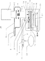
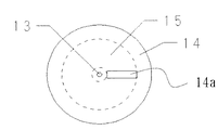
以下、添付図面を参照して、本発明の一実施形態としてのプラズマ処理装置100について説明する。ここで、図1は、プラズマ処理装置100の構造を示す概略断面図である。図2及び図3は、それぞれ、導波管2の接合部に設けられたマイクロ波に耐性のある隔壁シート4の平面図及び側面図である。図4は、マイクロ波供給器14の透過平面図であり、点線は環状導波路15を示し、角穴は導波管2の接合面を示している。図5は、矩形の開口部を有する金属平板16の平面図である。本実施形態のプラズマ処理装置100は、マイクロ波を利用して被処理物としての半導体基板21に所定のプラズマ処理(エッチング、成膜処理、レジストアッシング、ドーピング、シンタリング、表面改質処理等)を行う。
【0011】
プラズマ処理装置100は、マイクロ波発振器1と、導波管2と、マイクロ波供給器14と、金属平板16と、誘電体17と、ガス供給路18とを有する。
【0012】
マイクロ波発振器1は、例えば、調整されたマイクロ波を発振するマグネトロンからなり、2.45GHzのマイクロ波を発生する。マイクロ波は、その後、所定のモード(例えば、TMモードなど)に変換されて導波管2を伝搬する。なお、図1では、発生したマイクロ波がマイクロ波発振器1へ戻る反射波を吸収するアイソレータや、負荷側とのマッチングをとるためのインピーダンス整合器、被処理物Wを図示しないロードロック室との間で受け渡すためのゲートバルブなどは省略されている。
【0013】
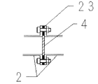
導波管2は、マイクロ波をマイクロ波供給器14に案内する機能を有する。導波管2には、後述する冷却媒体33の排出機構が接続される。排出機構は、穴群3と、隔壁シート4と、密閉部材5と、排気ホース7とが設けられている。
【0014】
穴群3は、隔壁シート4よりマイクロ波供給器14側にあって導波管2の表面に設けられており、導波管2内のマイクロ波を漏洩させない程度の多数の細かい、例えば、φ10mm以下、本実施形態ではφ3mmの穴から構成されている。
【0015】
隔壁シート4は、導波管2の接合部に設けられ、低誘電欠損材、例えば、厚み3mmのPTFEシートから構成されている。図2に示すように、隔壁シート4は、導波管2の合わせ面において、電気導通性のあるパッキン23と締結部品によって保持される。パッキン23の内側の形状は管内波長を変化させないように形状を導波管2の断面に対して同形状にする必要がある。本実施形態においては、図2に示すように、パッキン23の内側の形状は導波管2内の形状に適合している。但し、隔壁シート4を保持する必要があるので、保持部分は、マイクロ波伝播に悪影響しにくい数mm程度が望ましく、実施形態では、幅3mmで外側に向かって飛び出し、長さ3mm程度の窪みを設けた該パッキン23の窪みに隔壁シート4が保持されている。隔壁シート4により、誘電体17を冷却して高温になった冷却媒体33がマイクロ波発振器1や図示しないインピーダンス整合器に熱的に悪影響を与えることを防止することができる。
【0016】
密閉部材5は、穴群3を密閉する。排気ホース7は、密閉部材5に配置され、排出口6を介して冷却媒体33を排出する。
【0017】
マイクロ波供給器14は、その内部に形成されたプラズマ発生室19にマイクロ波を供給し、ガス供給路18を介して供給されるガスをプラズマ化して、プラズマ発生室19に収納されて半導体基板保持手段20によって保持された半導体基板21をプラズマ処理する。プラズマ発生室19は図示しない排気手段によって減圧又は真空環境に維持される。
【0018】
マイクロ波供給器14は、マイクロ波をプラズマ発生室19に供給するために、矩形の開口部14aを介して接続される環状導波路15と、金属平板16と、誘電体17を有する。また、プラズマ処理装置100は、誘電体17を冷却するための冷却機構を有する。
【0019】
金属平板16は、図5に示すように、マイクロ波を誘電体17に案内するための矩形の開口部又はスロット24を有し、例えば、アルミニウム、金、銀、銅などから構成される。金属平板16は、誘電体17が遊離してガスに不純物として混入することを防止したり、プラズマの分布を均一化したりする機能を有する。また、後述するように、平板16の中央には冷却媒体33を導入するための穴16aが設けられ、外周部にはマイクロ波に影響を及ぼさない形状を有し、冷却媒体33を排出する複数の穴16bが設けられ、マイクロ波供給器14より導入された冷却媒体33を誘電体17上面まで導入する。
【0020】
誘電体17は、マイクロ波をプラズマ発生室19に透過すると共にプラズマ発生室19の減圧又は真空環境を維持する。誘電体17は、例えば、アルミナセラミックス、アルミナイトライド、石英などから構成される。
【0021】
誘電体17の冷却機構は、図1に示すように、開閉バルブ8と、冷却媒体導入路10と、冷却媒体路11と、温度検出部12と、制御部22と、配管39とを有する。冷却媒体導入路10は、環状導波路15を有するマイクロ波供給器14の中央に継手9を介して設けられ、冷却媒体33を冷却媒体路11に導入する。また、図5に示すように、平板16の中央にも冷却媒体33を導入するための穴が設けられる。
【0022】
本実施形態では、平板16と誘電体17の間隔、即ち、冷却媒体路11の厚さは2mm以下であり、冷却媒体33は冷却媒体路11の空間を放射状に広がり、誘電体17の熱を冷却し、平板16の開口部、及び外周の穴から上部の環状導波路15へと流れ込み、環状導波路15を経由して導波管2へと流入する。この結果、冷却媒体33は、平板16も冷却し、スロット24の熱変形を防止する。
【0023】
導波管2に流れ込んだ冷却媒体33は、隔壁シート4によりそれ以上導波管2のマイクロ波発振器1側に流入することを拒まれ、φ3mmの穴群3を通して該導波管2の外部に排出される。排出された冷却媒体33は、密閉部材5を介してホース7を通して排出口6からプラズマ処理装置100外に排出される。この時、冷却媒体33は誘電体17で熱交換されているので高温になっており、高温媒体として排気処理するのが好ましい。
【0024】
誘電体17の温度調整機構は、開閉バルブ8と、温度検出器12と、制御部22と、図示しないメモリを含む。温度調節器12は、プラズマ発生室19の誘電体17近傍に設けられ、誘電体17近傍の温度を表す検出信号を制御部22に供給する。制御部22は、各部の動作を制御するが、本実施形態では特に、図示しないメモリに格納された温度制御方法に基づいてバルブ8の開閉及び開口量を制御する。この場合制御部の設定温度については、処理時に発生する昇華物、及び反応生成物のデポジションを防ぐ温度以上、かつ処理特性を阻害する誘電体温度の昇温を防止する温度以下の範囲に設定するのが好ましい。
【0025】
図示しないメモリに格納される温度制御方法は、例えば、温度検出器12が所定の温度を検出したかどうかを判断し、温度検出部12が所定の温度を検出したと判断した場合には、マイクロ波供給器14に接続された冷却媒体供給用の配管39上のバルブ8の開閉を制御するフローから構成される。より具体的には、制御部22は、温度検出器12からの検出信号が予め設定した温度に対して高いか低いかを判断し、高いと判断した場合には、制御部22は、バルブ8を開閉制御する図示しないバルブ開閉制御部にバルブ8の開閉及び開口量を調節させる信号を送信する。この結果、冷却媒体33の流量が調節される。バルブ開閉制御部と制御部22は一体であってもよい。
【0026】
本実施形態の温度調節機構によれば、誘電体17が規定の温度を超えた時だけ冷却媒体33を冷却媒体路11に送り込むことができるので誘電体17の温度を一定に維持して誘電体17の熱変形などを防止することができる。なお、制御部22は、ホース7から排出される冷却媒体33の流量を調節することもできる。この結果、制御部22は、冷却媒体33が冷却媒体路11に流入する量及び流出する量の両方を制御することができる。
【0027】
なお、冷却媒体33は、気体、液体又は低誘電欠損材を問わず、例えば、空気、窒素、アルゴン等の不活性ガス、フロリナート、ガルデン、HFE等のフッ素含有溶媒を含む。
【0028】
ガス供給路18には、反応ガス(例えば、NH3やNO)や放電ガス(例えば、XeやAr)が供給される。ガス供給路8には、例えば、図示しないガス供給源、バルブ、マスフローコントローラなどが接続される。
【0029】
以下、図6乃至図8を参照して、本発明の別の実施形態のプラズマ処理装置100Aについて説明する。ここで、図6は、プラズマ処理装置100Aの概略断面である。図7は、マイクロ波供給器34の平面図であり、同図に示すように、マイクロ波供給器34は、冷却水路30と入り口側及び出口側の継手31を有する。図8は、誘電体17上の熱伝導媒体シート29と金属平板16の開口部の位置を示す平面図である。なお、プラズマ処理装置100Aにおいて、プラズマ処理装置100と同一の部材は同一の参照番号を付して重複説明は省略する。
【0030】
本実施形態のプラズマ処理装置100は、冷却媒体路11の空間に熱伝導媒体シート29を配置している。シート29は耐熱性であり、熱伝導率の高い素材、例えば、シリコーンパウダーやシリコーンオイルから構成されている。また、図8に示すように、シート29は平板16の開口部24を閉口しないように誘電体17の外側周囲に配置される。
【0031】
冷却媒体導入路10を通り抜けた冷却媒体33は、誘電体17の中央から外側に向かって流れるため、誘電体17の中央と外側では冷却効率に差が生じる場合がある。プラズマ処理時間に対して誘電体17の蓄熱の差は大きく比例する。
【0032】
本実施形態では、誘電体17の外側に熱伝達率の良いシート29を設けることで誘電体17の外側の熱を平板16に伝達し、冷却媒体33による熱交換効率を向上している。また、マイクロ波供給器34に熱を逃がしている。
【0033】
マイクロ波供給器34は、図7に示すように、内部に周囲を取り囲むように冷却水路30を形成している。冷却水路30は、継手31を介して配管28に接続されており、マイクロ波供給器34内において冷却水の循環を行っている。熱伝導媒体シート29から平板16を介して伝わってきた誘電体17外側の熱は、冷却水路30にて排熱される。そのため冷却水路30は平板16近傍に設けられることが好ましい。
【0034】
誘電体17の近傍の温度検出器12によって検出された温度情報は制御部22に送られ、予め設定された温度によって、配管28上に設けられたバルブ32の開閉制御を行う。また、冷却媒体配管39上のバルブ8に対しても同様に開閉制御を行う。これにより、本実施形態は、プラズマ処理時間が長くなっても誘電体17の中央と外側の温度差を少なくした状態で一定に保つことができる。
【0035】
次に、プラズマ処理装置100及び100Aの動作について説明する。まず図示しない搬送アームが図示しないロードロック室から半導体基板20を図示しないゲートバルブを介してプラズマ発生室19の半導体基板保持手段21に導入する。この状態では、例えば、図示しないロードロック室とプラズマ発生室19とは真空又は減圧環境に維持されている。次いで、図示しないゲートバルブが閉口されてプラズマ発生室19は密閉される。必要があれば、保持手段21の高さの調節がなされてもよい。次いで、ガス供給路18の図示しないバルブが開口され、所定のガスがプラズマ発生室19に導入される。
【0036】
次に、マイクロ波発振器1からマイクロ波を導波管2を介してマイクロ波供給器14及び34に導入する。マイクロ波供給器14及び34に導入されたマイクロ波はプラズマ発生室19に導入されたガスをプラズマ化し、半導体基板20をプラズマ処理する。この結果、半導体基板20には予め設定された量の処理(例えば、所定の膜圧の成膜処理)が施される。
【0037】
プラズマ処理中に誘電体17の温度が所定の温度に到達したことを温度検出器12が検出すると、制御部22はバルブ8及び32を開口して冷却媒体33及び冷却水を導入し、誘電体17及び平板12を冷却する。この結果、誘電体17及び平板12が熱によって特性が劣化することを防止することができる。
【0038】
その後、半導体基板20は上述したのと逆の手順により図示しないゲートバルブを介してプラズマ発生室19からロードロック室に導出される。プラズマ発生室19から導出された半導体基板20は、必要があれば、次段のイオン注入装置などに搬送される。
【0039】
このように、本実施形態の誘電体17の冷却手段によれば、誘電体17のプラズマからの受熱による温度上昇での処理特性の変動を緩和することができ、半導体基板20へのエッチング処理、成膜処理、レジスト除去処理等に使用されるプラズマ処理装置100、100Aとしての処理特性の向上が可能である。
【0040】
本出願は更に以下の事項を開示する。
【0041】
(実施態様1) 被処理物を収納して真空又は減圧環境下で前記被処理物にプラズマ処理を施す真空容器と、
マイクロ波を前記真空容器に透過すると共に前記真空容器の前記減圧又は真空環境を維持する誘電体と、
前記マイクロ波を前記誘電体に案内するスロットを有する平板と、
前記平板と前記誘導体との間に配置された冷却路を含み、前記誘電体の温度を調節するための温度調節機構を有することを特徴とするプラズマ処理装置。
【0042】
(実施態様2) 前記冷却路が形成される前記平板と前記誘導体との間隔は2mm以下であることを特徴とする実施態様1記載のプラズマ処理装置。
【0043】
(実施形態3) 前記冷却路には、冷却媒体が供給されることを特徴とする実施態様1記載のプラズマ処理装置。
【0044】
(実施態様4) 前記冷却媒体は、空気、窒素、不活性ガス、フロリナート、ガルデン、フッ素含有溶媒のうち少なくとも一つを含むことを特徴とする実施態様3記載のプラズマ処理装置。
【0045】
(実施態様5) 前記冷却媒体は、気体、液体又は低誘電欠損材から構成されることを特徴とする実施態様3記載のプラズマ処理装置。
【0046】
(実施態様6) 前記冷却路には、冷却媒体が排出可能に供給されることを特徴とする実施態様1記載のプラズマ処理装置。
【0047】
(実施態様7) 前記誘電体又は当該誘電体近傍の温度を測定する温度検出器と、
当該温度検出器の温度に基づいて前記冷却路に供給される冷却媒体の流量を制御する制御部とを有することを特徴とする実施態様1記載のプラズマ処理装置。
【0048】
(実施態様8) 前記冷却路には熱伝導媒体が配置されることを特徴とする実施態様1又は3記載のプラズマ処理装置。
【0049】
(実施態様9) 前記熱伝導媒体は、前記誘電体の周囲に配置されることを特徴とする実施態様8記載のプラズマ処理装置。
【0050】
(実施態様10) 前記熱伝導媒体は、シリコーンパウダー又はシリコーンオイルを含むことを特徴とする実施態様8記載のプラズマ処理装置。
【0051】
(実施態様11) 前記熱伝導媒体は、誘電欠損材であることを特徴とする実施態様8記載のプラズマ処理装置。
【0052】
(実施態様12) 前記平板は、アルミニウム、金、銀及び銅の少なくとも一つを含む材料から構成されていることを特徴とする実施態様1記載のプラズマ処理装置。
【0053】
(実施態様13) 前記誘電体は、アルミナセラミックス、アルミナイトライド及び石英の少なくとも一つを含む材料から特徴されていることを特徴とする実施態様1記載のプラズマ処理装置。
【0054】
(実施態様14) 前記冷却媒体が透過することを許容すると共に前記マイクロ波が透過することを防止する多数の孔を所定の部位に有し、前記マイクロ波を前記平板まで案内する導波管と、
前記導波管の前記所定の部位と前記マイクロ波を供給するマイクロ波供給源との間であって前記導波管に設けられ、前記冷却媒体が前記導波管を前記マイクロ波供給源に向かって移動することを防止する隔壁とを更に有することを特徴とする実施態様3記載のプラズマ処理装置。
【0055】
(実施態様15) 前記隔壁は、誘電欠損材から構成されていることを特徴とする実施態様3記載のプラズマ処理装置。
【0056】
(実施態様16) 被処理物を真空容器に収納して真空又は減圧環境下で前記被処理物にプラズマ処理を施すプラズマ処理方法であって、
マイクロ波を前記真空容器に透過すると共に前記真空容器の前記減圧又は真空環境を維持する誘電体の近傍の温度を検出するステップと、
前記検出ステップの検出結果に基づいて、前記マイクロ波を前記誘電体に案内するスロットを有する平板と前記誘導体との間に配置された冷却路の冷却媒体の流量を制御するステップとを有することを特徴とするプラズマ処理方法。
【0057】
【発明の効果】
以上説明したように、本発明によれば、誘電体の受熱による影響を防止して高品位なプラズマ処理を被処理物に施すプラズマ処理装置及び方法を提供することができる。
【図面の簡単な説明】
【図1】 本発明の一実施形態のプラズマ処理装置の構造を示す概略断面図である。
【図2】 図1に示すプラズマ装置に設けられた導波管の接合部に設けられた隔壁シートの平面図である。
【図3】 図2に示す隔壁シート付近の側面図である。
【図4】 図1に示すプラズマ装置に設けられたマイクロ波供給器の透過平面図である。
【図5】 図1に示すプラズマ装置に設けられた金属平板の平面図である。
【図6】 本発明の別の実施形態のプラズマ処理装置の構造を示す概略断面図である。
【図7】 図6に示すプラズマ装置に設けられたマイクロ波供給器の透過平面図である。
【図8】 図6に示すプラズマ装置に設けられた熱伝導媒体シートの平面図である。
【符号の説明】
1 マイクロ波発振器
2 導波管
3 穴群
4 隔壁シート
5 密閉部材
6 冷却媒体排出口
7 排気ホース
8 バルブ
10 冷却媒体導入路
11 冷却媒体路
12 温度検出器
14、34 マイクロ波供給器
15 環状導波路
16 金属平板
17 誘電体
19 プラズマ発生室
21 半導体基板
22 制御部
29 熱伝導媒体シート
30 冷却水路
33 冷却媒体
100、100A プラズマ処理装置[0001]
BACKGROUND OF THE INVENTION
The present invention relates to plasma processing using plasma generated using microwaves, and more particularly to cooling a dielectric that transmits microwaves to a plasma generation chamber and maintains a reduced pressure or vacuum environment in the plasma generation chamber.
[0002]
[Prior art]
In the manufacture of semiconductor elements, in order to form elements on a semiconductor single crystal substrate (hereinafter referred to as a substrate) such as silicon, a photosensitive resin is applied to the substrate surface with a coating apparatus and prepared in advance with an exposure apparatus. A mask (reticle) pattern is exposed and transferred, and development processing is performed by a developing device to obtain a target photosensitive resin transfer pattern. Using this transfer pattern as a mask, the substrate or the like is subjected to a desired process in the subsequent etching, diffusion, film formation process, etc., and an element is formed.
[0003]
In a semiconductor processing process, a plasma processing apparatus is indispensable, and at the same time, high processing speed and low damage are required to improve productivity. In recent years, as a means to achieve the required high processing speed and low damage, a method of generating high-density plasma on the dielectric surface on the vacuum side by introducing microwaves into the dielectric from slots machined into metal flat plates has attracted attention. ing.
[0004]
Conventional plasma processing apparatuses typically supply microwaves supplied from a microwave generation source to a plasma generation chamber that houses a semiconductor substrate as an object to be processed through a metal plate having a slot and a dielectric. To do. The plasma generation chamber is maintained in a reduced pressure or vacuum environment and supplied with a reaction gas. The reactive gas is turned into plasma by microwaves, becomes radicals and ions with strong activity, reacts with the semiconductor substrate, and is subjected to plasma treatment. The dielectric has a function of transmitting microwaves to the plasma generation chamber and maintaining a reduced pressure or vacuum environment of the plasma generation chamber. The metal flat plate has a function of introducing a microwave into the dielectric through the slot to prevent the dielectric from being liberated and entering the gas as an impurity, or to make the plasma distribution uniform. Such a plasma processing method can generate microwave-excited high-density plasma on the dielectric surface on the vacuum side, and is very promising as a large-area and high-density plasma generation method.
[0005]
[Problems to be solved by the invention]
However, in the conventional plasma processing method, when the plasma is generated, the dielectric becomes high temperature due to heat reception, and the temperature of the dielectric rises, and the following processing characteristics change due to the temperature drop of the dielectric immediately after the device is idle, and the device malfunction can occur. There was sex.
[0006]
Examples of defects in processing characteristics include the following. That is, the surface of the photoresist after the high-concentration ion implantation is altered and a hardened layer is formed. For this reason, when the wafer is heated to a temperature higher than the resist baking temperature after the lithography process, a phenomenon in which the resist pops off (also referred to as “popping”) occurs. Resist that flies off by heating remains on the wafer even if overashing is performed thereafter, which greatly affects the chip yield. Therefore, the ashing after the high-concentration ion implantation needs to be performed at a wafer temperature equal to or lower than the resist baking temperature after the lithography process. Therefore, in processing with a device that does not have a dielectric temperature adjustment function, the temperature of the dielectric increases each time the above process is repeated, and as a result, the processed wafer becomes higher than the resist baking temperature after the lithographic process by radiant heat from the dielectric. This causes a problem that a phenomenon of popping up the resist (popping) occurs.
[0007]
Examples of problems on the apparatus side include the following. That is, in a vacuum processing apparatus using a dielectric, a seal member is used between the dielectric and the vacuum vessel member for the purpose of maintaining a vacuum with the outside. Generally, a fluororubber sealant, a perfluoroelastomer sealant, or the like is used for this seal member, but the maximum operating temperature is 200 ° C. or less because of the physical properties of the material. Therefore, in a device that does not have a dielectric temperature adjustment function, the dielectric temperature rises each time processing is performed, and the dielectric temperature rises above the maximum operating temperature of the sealing material. As a result, the sealing material performs the vacuum holding function. It was gone. In addition, in a device that does not have a dielectric temperature control function, when used after a long idle state, the dielectric and the inner wall of the dielectric holding part are sublimated from the processing wafer, and the reaction product is generated from the gas. Since it is below the temperature at which it changes to a solid, it is not evacuated in a gas state, and deposition occurs on the dielectric and the inner wall of the dielectric holding part. As a result, the accumulated deposition has a great influence on the chip yield by reattaching to the processed wafer.
[0008]
An object of the present invention is to provide a plasma processing apparatus and method for performing a high-quality plasma treatment on an object to be processed while preventing the influence of heat received by a dielectric material in order to solve the problems of the prior art. And
[0009]
[Means for Solving the Problems]
A plasma processing apparatus according to one aspect of the present invention includes a vacuum container that accommodates an object to be processed and performs plasma processing on the object to be processed in a vacuum or a reduced pressure environment, and transmits a microwave to the vacuum container and the vacuum. A dielectric that maintains the reduced pressure or vacuum environment of the container, a flat plate having a slot for guiding the microwave to the dielectric, and a cooling path disposed between the flat plate and the derivative; has a temperature adjusting mechanism for adjusting the temperature, the distance between the flat plate cooling passage is formed and the derivative Ri der below 2 mm, the temperature of measuring the dielectric or the temperature of the dielectric near characterized Rukoto of having a control unit for controlling the flow rate of the cooling medium supplied to the cooling passage based on the measured temperature by the detector and the temperature detector.
[0010]
DETAILED DESCRIPTION OF THE INVENTION
Hereinafter, a
[0011]
The
[0012]
The
[0013]
The
[0014]
The
[0015]
The
[0016]
The sealing
[0017]
The
[0018]
The
[0019]
As shown in FIG. 5, the metal
[0020]
The dielectric 17 transmits microwaves to the
[0021]
As shown in FIG. 1, the cooling mechanism for the dielectric 17 includes an opening /
[0022]
In the present embodiment, the distance between the
[0023]
The cooling
[0024]
The temperature adjustment mechanism of the dielectric 17 includes the opening /
[0025]
The temperature control method stored in a memory (not shown) is, for example, determining whether or not the
[0026]
According to the temperature adjustment mechanism of the present embodiment, the cooling
[0027]
The cooling
[0028]
A reactive gas (for example, NH 3 or NO) or a discharge gas (for example, Xe or Ar) is supplied to the
[0029]
Hereinafter, a
[0030]
In the
[0031]
Since the cooling
[0032]
In the present embodiment, by providing a
[0033]
As shown in FIG. 7, the
[0034]
The temperature information detected by the
[0035]
Next, the operation of the
[0036]
Next, the microwave is introduced from the
[0037]
When the
[0038]
Thereafter, the
[0039]
As described above, according to the cooling means for the dielectric 17 of the present embodiment, it is possible to mitigate fluctuations in processing characteristics due to a temperature rise due to heat reception from the plasma of the dielectric 17, and to etch the
[0040]
The present application further discloses the following matters.
[0041]
(Embodiment 1) A vacuum container that accommodates an object to be processed and performs plasma processing on the object to be processed in a vacuum or a reduced pressure environment;
A dielectric that transmits microwaves to the vacuum vessel and maintains the reduced pressure or vacuum environment of the vacuum vessel;
A flat plate having a slot for guiding the microwave to the dielectric;
A plasma processing apparatus comprising a cooling path disposed between the flat plate and the derivative, and having a temperature adjusting mechanism for adjusting the temperature of the dielectric.
[0042]
(Embodiment 2) The plasma processing apparatus according to
[0043]
(Embodiment 3) The plasma processing apparatus according to
[0044]
(Embodiment 4) The plasma processing apparatus according to
[0045]
(Embodiment 5) The plasma processing apparatus according to
[0046]
(Embodiment 6) The plasma processing apparatus according to
[0047]
(Embodiment 7) A temperature detector for measuring a temperature of the dielectric or the vicinity of the dielectric,
The plasma processing apparatus according to
[0048]
(Embodiment 8) The plasma processing apparatus according to
[0049]
(Embodiment 9) The plasma processing apparatus according to
[0050]
(Embodiment 10) The plasma processing apparatus according to
[0051]
(Embodiment 11) The plasma processing apparatus according to
[0052]
(Embodiment 12) The plasma processing apparatus according to
[0053]
(Embodiment 13) The plasma processing apparatus according to
[0054]
(Embodiment 14) A waveguide that guides the microwave to the flat plate, having a plurality of holes in a predetermined portion that allows the cooling medium to pass therethrough and prevents the microwave from passing therethrough ,
Between the predetermined portion of the waveguide and a microwave supply source that supplies the microwave, and is provided in the waveguide, and the cooling medium directs the waveguide toward the microwave supply source. The plasma processing apparatus according to
[0055]
(Embodiment 15) The plasma processing apparatus according to
[0056]
(Embodiment 16) A plasma processing method for storing an object to be processed in a vacuum vessel and performing plasma processing on the object to be processed in a vacuum or reduced pressure environment,
Detecting a temperature in the vicinity of a dielectric that transmits microwaves to the vacuum vessel and maintains the reduced pressure or vacuum environment of the vacuum vessel;
Controlling a flow rate of a cooling medium in a cooling path arranged between the flat plate having a slot for guiding the microwave to the dielectric and the derivative based on a detection result of the detection step. A plasma processing method.
[0057]
【The invention's effect】
As described above, according to the present invention, it is possible to provide a plasma processing apparatus and method for preventing an influence due to heat reception of a dielectric and performing high-quality plasma processing on an object to be processed.
[Brief description of the drawings]
FIG. 1 is a schematic cross-sectional view showing the structure of a plasma processing apparatus according to an embodiment of the present invention.
2 is a plan view of a partition sheet provided at a junction of a waveguide provided in the plasma apparatus shown in FIG.
FIG. 3 is a side view of the vicinity of the partition sheet shown in FIG.
FIG. 4 is a transmission plan view of a microwave supply device provided in the plasma apparatus shown in FIG.
FIG. 5 is a plan view of a metal flat plate provided in the plasma apparatus shown in FIG.
FIG. 6 is a schematic sectional view showing the structure of a plasma processing apparatus according to another embodiment of the present invention.
7 is a transmission plan view of a microwave supply device provided in the plasma apparatus shown in FIG. 6. FIG.
8 is a plan view of a heat conductive medium sheet provided in the plasma apparatus shown in FIG. 6. FIG.
[Explanation of symbols]
DESCRIPTION OF
Claims (13)
マイクロ波を前記真空容器に透過すると共に前記真空容器の前記減圧又は真空環境を維持する誘電体と、
前記マイクロ波を前記誘電体に案内するスロットを有する平板と、
前記平板と前記誘導体との間に配置された冷却路を含み、前記誘電体の温度を調節するための温度調節機構を有し、
前記冷却路が形成される前記平板と前記誘導体との間隔は2mm以下であり、
前記誘電体又は当該誘電体近傍の温度を測定する温度検出器と、
当該温度検出器によって測定された温度に基づいて前記冷却路に供給される冷却媒体の流量を制御する制御部とを有することを特徴とするプラズマ処理装置。A vacuum container for storing the object to be processed and performing a plasma treatment on the object to be processed in a vacuum or reduced pressure environment;
A dielectric that transmits microwaves to the vacuum vessel and maintains the reduced pressure or vacuum environment of the vacuum vessel;
A flat plate having a slot for guiding the microwave to the dielectric;
A cooling path disposed between the flat plate and the derivative; and a temperature adjusting mechanism for adjusting the temperature of the dielectric,
A distance between the flat plate and the derivatives in which the cooling channel is formed Ri der below 2 mm,
A temperature detector for measuring the temperature of the dielectric or the vicinity of the dielectric;
The plasma processing apparatus according to claim Rukoto of having a control unit for controlling the flow rate of the cooling medium supplied to the cooling passage based on a temperature measured by the temperature detector.
前記導波管の前記所定の部位と前記マイクロ波を供給するマイクロ波供給源との間であって前記導波管に設けられ、前記冷却媒体が前記導波管を前記マイクロ波供給源に向かって移動することを防止する隔壁とを更に有することを特徴とする請求項2記載のプラズマ処理装置。A waveguide for allowing the cooling medium to pass therethrough and preventing the microwave from passing therethrough in a predetermined portion, and guiding the microwave to the flat plate;
Between the predetermined portion of the waveguide and a microwave supply source that supplies the microwave, and is provided in the waveguide, and the cooling medium directs the waveguide toward the microwave supply source. The plasma processing apparatus according to claim 2, further comprising a partition wall that prevents movement of the plasma processing apparatus.
Priority Applications (3)
| Application Number | Priority Date | Filing Date | Title |
|---|---|---|---|
| JP2002351756A JP4136630B2 (en) | 2002-12-03 | 2002-12-03 | Plasma processing equipment |
| KR1020030086759A KR100593291B1 (en) | 2002-12-03 | 2003-12-02 | Plasma processing apparatus and method |
| US10/725,403 US7140321B2 (en) | 2002-12-03 | 2003-12-03 | Plasma processing apparatus and method |
Applications Claiming Priority (1)
| Application Number | Priority Date | Filing Date | Title |
|---|---|---|---|
| JP2002351756A JP4136630B2 (en) | 2002-12-03 | 2002-12-03 | Plasma processing equipment |
Publications (3)
| Publication Number | Publication Date |
|---|---|
| JP2004186440A JP2004186440A (en) | 2004-07-02 |
| JP2004186440A5 JP2004186440A5 (en) | 2006-01-19 |
| JP4136630B2 true JP4136630B2 (en) | 2008-08-20 |
Family
ID=32588081
Family Applications (1)
| Application Number | Title | Priority Date | Filing Date |
|---|---|---|---|
| JP2002351756A Expired - Fee Related JP4136630B2 (en) | 2002-12-03 | 2002-12-03 | Plasma processing equipment |
Country Status (3)
| Country | Link |
|---|---|
| US (1) | US7140321B2 (en) |
| JP (1) | JP4136630B2 (en) |
| KR (1) | KR100593291B1 (en) |
Families Citing this family (21)
| Publication number | Priority date | Publication date | Assignee | Title |
|---|---|---|---|---|
| JP4612786B2 (en) * | 2003-03-03 | 2011-01-12 | キヤノン株式会社 | Manufacturing method of organic field effect transistor |
| ATE492912T1 (en) * | 2003-04-01 | 2011-01-15 | Canon Kk | ORGANIC SEMICONDUCTOR ARRANGEMENT |
| JP2005079204A (en) * | 2003-08-28 | 2005-03-24 | Canon Inc | Field effect transistor and its manufacturing method |
| JP4401826B2 (en) * | 2004-03-10 | 2010-01-20 | キヤノン株式会社 | Field effect transistor and manufacturing method thereof |
| JP4557755B2 (en) * | 2004-03-11 | 2010-10-06 | キヤノン株式会社 | Substrate, conductive substrate, and organic field effect transistor manufacturing method |
| JP4401836B2 (en) * | 2004-03-24 | 2010-01-20 | キヤノン株式会社 | Field effect transistor and manufacturing method thereof |
| JP4731840B2 (en) * | 2004-06-14 | 2011-07-27 | キヤノン株式会社 | Field effect transistor and manufacturing method thereof |
| US7511296B2 (en) * | 2005-03-25 | 2009-03-31 | Canon Kabushiki Kaisha | Organic semiconductor device, field-effect transistor, and their manufacturing methods |
| JP2006294422A (en) * | 2005-04-11 | 2006-10-26 | Tokyo Electron Ltd | Plasma treatment apparatus, slot antenna and plasma treatment method |
| US7435989B2 (en) * | 2005-09-06 | 2008-10-14 | Canon Kabushiki Kaisha | Semiconductor device with layer containing polysiloxane compound |
| US7695999B2 (en) * | 2005-09-06 | 2010-04-13 | Canon Kabushiki Kaisha | Production method of semiconductor device |
| JP2008071500A (en) * | 2006-09-12 | 2008-03-27 | Noritsu Koki Co Ltd | Plasma generating device and work processing device using it |
| WO2008123605A1 (en) * | 2007-03-29 | 2008-10-16 | Tokyo Electron Limited | Plasma process apparatus |
| KR100856552B1 (en) * | 2007-06-21 | 2008-09-04 | (주)아이씨디 | Plasma treatment apparatus |
| JP4793662B2 (en) * | 2008-03-28 | 2011-10-12 | 独立行政法人産業技術総合研究所 | Microwave plasma processing equipment |
| US9390941B2 (en) | 2009-11-17 | 2016-07-12 | Hitachi High-Technologies Corporation | Sample processing apparatus, sample processing system, and method for processing sample |
| US9978565B2 (en) | 2011-10-07 | 2018-05-22 | Lam Research Corporation | Systems for cooling RF heated chamber components |
| US9530656B2 (en) | 2011-10-07 | 2016-12-27 | Lam Research Corporation | Temperature control in RF chamber with heater and air amplifier |
| KR102102003B1 (en) * | 2012-05-25 | 2020-04-20 | 도쿄엘렉트론가부시키가이샤 | Plasma processing device and plasma processing method |
| US9048190B2 (en) * | 2012-10-09 | 2015-06-02 | Applied Materials, Inc. | Methods and apparatus for processing substrates using an ion shield |
| TWI623960B (en) * | 2013-03-27 | 2018-05-11 | 蘭姆研究公司 | Semiconductor manufacturing apparatus and method for processing the same |
Family Cites Families (7)
| Publication number | Priority date | Publication date | Assignee | Title |
|---|---|---|---|---|
| JPH02302507A (en) * | 1989-05-16 | 1990-12-14 | Matsushita Electric Ind Co Ltd | High-frequency incinerator |
| JPH08274067A (en) | 1995-03-30 | 1996-10-18 | Hitachi Ltd | Plasma generating device |
| US6059922A (en) | 1996-11-08 | 2000-05-09 | Kabushiki Kaisha Toshiba | Plasma processing apparatus and a plasma processing method |
| JPH10340892A (en) | 1997-06-06 | 1998-12-22 | Sumitomo Metal Ind Ltd | Plasma-processing device |
| JP4053173B2 (en) * | 1999-03-29 | 2008-02-27 | 東京エレクトロン株式会社 | Microwave plasma processing apparatus and method |
| JP2002134417A (en) * | 2000-10-23 | 2002-05-10 | Tokyo Electron Ltd | Plasma processing system |
| JP3890258B2 (en) * | 2001-05-28 | 2007-03-07 | キヤノン株式会社 | Electron source manufacturing method and electron source manufacturing apparatus |
-
2002
- 2002-12-03 JP JP2002351756A patent/JP4136630B2/en not_active Expired - Fee Related
-
2003
- 2003-12-02 KR KR1020030086759A patent/KR100593291B1/en not_active IP Right Cessation
- 2003-12-03 US US10/725,403 patent/US7140321B2/en not_active Expired - Fee Related
Also Published As
| Publication number | Publication date |
|---|---|
| US7140321B2 (en) | 2006-11-28 |
| JP2004186440A (en) | 2004-07-02 |
| US20040118520A1 (en) | 2004-06-24 |
| KR20040048838A (en) | 2004-06-10 |
| KR100593291B1 (en) | 2006-06-26 |
Similar Documents
| Publication | Publication Date | Title |
|---|---|---|
| JP4136630B2 (en) | Plasma processing equipment | |
| US7629033B2 (en) | Plasma processing method for forming a silicon nitride film on a silicon oxide film | |
| KR100920280B1 (en) | Processing apparatus | |
| US8006640B2 (en) | Plasma processing apparatus and plasma processing method | |
| US7396771B2 (en) | Plasma etching apparatus and plasma etching method | |
| JP4624856B2 (en) | Plasma processing equipment | |
| US7947189B2 (en) | Vacuum processing apparatus and vacuum processing method of sample | |
| WO2007015504A1 (en) | Plasma processing apparatus and gas permeable plate | |
| WO2006092985A1 (en) | Microwave plasma processing device | |
| US5389197A (en) | Method of and apparatus for plasma processing of wafer | |
| KR100886030B1 (en) | Processing apparatus and lid opening/closing mechanism | |
| US6729261B2 (en) | Plasma processing apparatus | |
| US20070163502A1 (en) | Substrate processing apparatus | |
| EP1069597B1 (en) | Apparatus and method for manufacturing semiconductor device | |
| JP2012049393A (en) | Plasma processing apparatus | |
| US11942308B2 (en) | Microwave plasma source, microwave plasma processing apparatus and plasma processing method | |
| KR20130018822A (en) | Plasma nitriding treatment method and plasma nitriding treatment device | |
| JP5155790B2 (en) | Substrate mounting table and substrate processing apparatus using the same | |
| JP2007250569A (en) | Plasma treatment apparatus and member to be exposed in plasma | |
| JP5090299B2 (en) | Plasma processing apparatus and substrate mounting table | |
| JP3675065B2 (en) | Dry etching method | |
| KR100597627B1 (en) | Plasma reaction chamber | |
| JP5249689B2 (en) | Plasma processing apparatus and substrate mounting table | |
| JP2721888B2 (en) | Low pressure vapor phase growth equipment | |
| JP2000082694A (en) | Plasma processing apparatus |
Legal Events
| Date | Code | Title | Description |
|---|---|---|---|
| A521 | Request for written amendment filed |
Free format text: JAPANESE INTERMEDIATE CODE: A523 Effective date: 20051130 |
|
| A621 | Written request for application examination |
Free format text: JAPANESE INTERMEDIATE CODE: A621 Effective date: 20051130 |
|
| A977 | Report on retrieval |
Free format text: JAPANESE INTERMEDIATE CODE: A971007 Effective date: 20071128 |
|
| A131 | Notification of reasons for refusal |
Free format text: JAPANESE INTERMEDIATE CODE: A131 Effective date: 20071204 |
|
| A521 | Request for written amendment filed |
Free format text: JAPANESE INTERMEDIATE CODE: A523 Effective date: 20080131 |
|
| TRDD | Decision of grant or rejection written | ||
| A01 | Written decision to grant a patent or to grant a registration (utility model) |
Free format text: JAPANESE INTERMEDIATE CODE: A01 Effective date: 20080513 |
|
| A01 | Written decision to grant a patent or to grant a registration (utility model) |
Free format text: JAPANESE INTERMEDIATE CODE: A01 |
|
| A61 | First payment of annual fees (during grant procedure) |
Free format text: JAPANESE INTERMEDIATE CODE: A61 Effective date: 20080603 |
|
| R150 | Certificate of patent or registration of utility model |
Free format text: JAPANESE INTERMEDIATE CODE: R150 |
|
| FPAY | Renewal fee payment (event date is renewal date of database) |
Free format text: PAYMENT UNTIL: 20110613 Year of fee payment: 3 |
|
| FPAY | Renewal fee payment (event date is renewal date of database) |
Free format text: PAYMENT UNTIL: 20120613 Year of fee payment: 4 |
|
| FPAY | Renewal fee payment (event date is renewal date of database) |
Free format text: PAYMENT UNTIL: 20120613 Year of fee payment: 4 |
|
| FPAY | Renewal fee payment (event date is renewal date of database) |
Free format text: PAYMENT UNTIL: 20130613 Year of fee payment: 5 |
|
| LAPS | Cancellation because of no payment of annual fees |