JP4136063B2 - Radiation imaging device - Google Patents
Radiation imaging device Download PDFInfo
- Publication number
- JP4136063B2 JP4136063B2 JP11481698A JP11481698A JP4136063B2 JP 4136063 B2 JP4136063 B2 JP 4136063B2 JP 11481698 A JP11481698 A JP 11481698A JP 11481698 A JP11481698 A JP 11481698A JP 4136063 B2 JP4136063 B2 JP 4136063B2
- Authority
- JP
- Japan
- Prior art keywords
- image
- data
- memory
- radiation imaging
- imaging apparatus
- Prior art date
- Legal status (The legal status is an assumption and is not a legal conclusion. Google has not performed a legal analysis and makes no representation as to the accuracy of the status listed.)
- Expired - Fee Related
Links
- 230000005855 radiation Effects 0.000 title claims description 27
- 238000003384 imaging method Methods 0.000 title claims description 22
- 230000015654 memory Effects 0.000 claims description 63
- 230000006835 compression Effects 0.000 claims description 9
- 238000007906 compression Methods 0.000 claims description 9
- 230000002093 peripheral effect Effects 0.000 claims description 5
- 238000000034 method Methods 0.000 claims description 4
- 239000004065 semiconductor Substances 0.000 claims description 3
- 238000001514 detection method Methods 0.000 description 7
- 238000010586 diagram Methods 0.000 description 6
- 238000000605 extraction Methods 0.000 description 6
- 238000006243 chemical reaction Methods 0.000 description 3
- 230000007274 generation of a signal involved in cell-cell signaling Effects 0.000 description 3
- 239000010408 film Substances 0.000 description 2
- 239000011159 matrix material Substances 0.000 description 2
- VYPSYNLAJGMNEJ-UHFFFAOYSA-N Silicium dioxide Chemical compound O=[Si]=O VYPSYNLAJGMNEJ-UHFFFAOYSA-N 0.000 description 1
- 230000002950 deficient Effects 0.000 description 1
- 238000002059 diagnostic imaging Methods 0.000 description 1
- 230000000694 effects Effects 0.000 description 1
- 238000005516 engineering process Methods 0.000 description 1
- 239000000284 extract Substances 0.000 description 1
- 238000013507 mapping Methods 0.000 description 1
- 238000004886 process control Methods 0.000 description 1
- 230000004044 response Effects 0.000 description 1
- 239000010409 thin film Substances 0.000 description 1
Images


Description
【0001】
【発明の属する技術分野】
本発明は、撮像し記憶されたX線デジタル画像を表示する装置を備えた放射線撮像装置に関する。
【0002】
【従来の技術】
医用画像診断機器分野においてはデジタル技術が急速に進歩し、単純X線撮影装置に使用されていたX線フィルムやイメージングプレートに代わり半導体のX線面センサーを用いた放射線画像検出器が開発されている。このX線面センサーは、通常、X線を光に変換するX線変換膜と、ホトダイオードアレイと、TFTスイツチによって構成されており、X線照射後、各画素に蓄積された信号電荷を読み出しX線画像を形成する様になっている。
【0003】
一般的な画像の記憶装置に取込む方法とそれを表示装置に表示する方法を、図4、図5で説明する。図4の放射線画像検出部は、X線画像の一画素として、X線を光に変えるシンチレータとその光を受けて電荷信号を発生するホトダイオードとからなる光電変換部と、その信号をスイッチングして外部に出す薄膜トランジスタTFTとから構成されている。所定の寸法にこの画素がどれほど配列されているかによって、画像の分解能が幾何学的に決定される。そしてその電荷パターンを信号読出し回路の走査パルス発生器により走査線に信号を順次送って、TFTをスイッチングし、そのホトダイオードの電荷信号を信号線を介して順次転送レジスタに送り込む。
【0004】
転送レジスタから画像メモリ(RAM)の入力バッファに、時系列にX線電荷画像信号が入力される。制御バスからのWRITE入力信号とチップセレクタ信号により書込回路が働き、データはマトリックス構成のメモリセルに入る。このマトリックスメモリセルは画像一ページ分に相当するバッファメモリでページメモリ(フレームメモリ)として使用されている。画像の大きさによりそのメモリサイズが決定され、その画素サイズは例えば2048×2048と表現される。
このフレームメモリの画像を保管する場合は、制御バスからのREAD入力信号とチップセレクタ信号により、大型の画像記憶装置(磁気ディスク)にデータバスで転送され、撮像毎にこのルートで記録される。
【0005】
次に画像表示装置(CRT)に表示する場合は、同じく制御バスからのREAD入力信号とチップセレクタ信号によりフレームメモリからの読出しを行なう。図5に示すデータ読出部60が、アドレスレジスタに格納されているフレームメモリの読出開始原点、およびフレームメモリのサイズ(横方向と縦方向)によりアドレス制御Bをして、メモリー内の画像データを読み出しレジスタBに取り込み(読み出し手段)、データバスでリフレッシュメモリB20(RAMビデオメモリ)に順次ストアする。
【0006】
そして、メモリ制御9は表示タイミング発生部10からの信号でリフレッシュメモリB20の読出し制御信号を発生し、一方ビデオ信号発生部B23はリフレッシュメモリB20からの読出し信号、表示タイミング発生部10からの表示タイミング信号を受けて、ビデオ信号を発生する。表示装置CRT−B26はビデオ信号を受けてノンインタレース走査もしくはインタレース走査で画像を表示する。
【0007】
また必要により、同様な方法で画像ハードコピー装置5に出力する。
【0008】
【発明が解決しようとする課題】
従来の放射線撮像装置は以上のように構成されているが、放射線画像検出部1から出力された画像データは一旦バッファメモリ3(フレームメモリ)に転送され、画像記憶装置(磁気ディスク)4や画像表示装置CRT−B26や画像ハードコピー装置5に転送されるが、画像表示装置CRTには、医療用高解像度モニタからパーソナルコンピュータ用低解像度モニタまで、さまざまな解像度をもったものがあり、出力画像のサイズが必ずしもマッチしないという問題があった。特に放射線画像検出部1が動画像と静止画像の両方の撮像を目的としている場合には、例えば動画の場合にはビデオモニタへ、静止画の場合にはレーザイメージャへ出力するというような時、異なる解像度のデバイスに対応できるデータ転送手段が必要となっている。
【0009】
本発明は、このような事情に鑑みてなされたものであって、解像度の異なるデバイスに同時もしくは順次、画像データを転送して表示もしくは記録することのできる放射線画像撮像装置を提供することを目的とする。
【0010】
【課題を解決するための手段】
上記の目的を達成するため、本発明の放射線撮像装置は、一次元または二次元の半導体放射線センサーアレイを備えた放射線撮像装置において、撮影された画素データを格納するメモリーと、メモリー内の画素データを読み出すためのデータ読み出し手段と、
前記データ読み出し手段から読み出された画素データを入力する演算手段と、前記演算手段で演算された画素データをストアする複数のリフレッシュメモリと、前記複数のリフレッシュメモリのそれぞれに接続されたビデオ信号発生部と、前記ビデオ信号発生部のそれぞれに接続され、画像を表示する画像表示装置とを具備し、前記演算手段が前記それぞれの画像表示装置の解像度に対応させて画像を圧縮または拡大演算処理することを特徴とする。
【0011】
また、データ読み出し手段が画像データの一部特定の画素データのみを読み出すことを特徴とする。
【0012】
また、解像度の異なる前記画像表示装置に対して、その異なる数だけ設けられた処理制御ラインを有することを特徴とする。
【0013】
また、画像表示装置が動画像表示装置と静止画像表示装置とで構成されていることを特徴とする。
【0014】
また、撮像された画素データがメモリー内に無い部分に対し、その周辺部の画素データを用いて補間し縮小(拡大)演算することを特徴とする。
【0015】
本発明の放射線撮像装置は上記のように構成されており、演算手段が縮小または拡大演算処理をしたり、データ読み出し手段が画像データの一部特定の画素データのみを読み出したり、撮像された画素データの欠落がある部分に対し周辺部のデータで補間演算をしたり、解像度の異なる表示装置に応じて複数個の演算手段を備え、また動画像と静止画像を、同時もしくは順次、表示装置に必要な画像を表示することができる。
【0016】
【発明の実施の形態】
本発明の放射線撮像装置の一実施例を図1により説明する。
【0017】
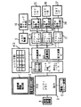
図1において、本放射線撮像装置は放射線画像検出部1と信号読出回路2とからなる画像発生部と、その画像を一時的に取り込むバッファメモリ3(フレームメモリ)と画像記憶装置4とからなる画像メモリ部と、バッファメモリ3の画像データを処理制御して表示装置CRT−A25、B26、C27に転送する処理制御部から構成される。
【0018】
処理制御部は、バッファメモリ3のアドレス値を格納しているレジスタ部40と、バッファメモリ3の画像データを読み出すデータ読出部60と、読み出したデータを圧縮演算Aまたは拡大演算Cする演算部50と、表示装置の解像度に対応したメモリサイズのリフレッシュメモリ(RAMビデオメモリ)A19、B20、C21と、ビデオ信号発生部A22、B23、C24と、各ラインの表示のタイミングを取るための表示タイミング発生部10と、リフレッシュメモリのメモリ制御9と、解像度の異なる画像表示装置25、26、27から構成される。
次に処理制御部の信号の流れについて説明する。データ読出部60はバッファメモリ3の画像データを、レジスタ部40に格納されている各アドレスレジスタ値(41、42)、(43、44)にしたがってアドレス制御A、B、Cをしてメモリー内の画像データを、読み出しレジスタA、B、Cに取り込み(読み出し手段)、データバスで演算部50に送る。
【0019】
本発明では、レジスタ部40の各アドレスレジスタに読出開始原点(41、42)、元画像即ちフレームメモリ3のサイズ(横方向43と縦方向44)、出力画像サイズ(横方向45と縦方向46)がそれぞれ格納されている。データ読出部60と演算部50は、格納されたアドレスレジスタの値により、フレームメモリの画像データを読み出し、演算処理する。
【0020】
演算部50はレジスタ部40のレジスタ値(45、46)に従い、表示装置の解像度にあわせた圧縮拡大演算A、C処理をし、データバスでリフレッシュメモリA19、B20、C21(RAMビデオメモリ)にデータを順次ストアする。
処理制御部は、解像度の異なる画像表示装置に対して、その異なる数だけの処理制御ラインを設け、データ読取部60―演算部50―リフレッシュメモリA、B、C、―ビデオ信号発生部A、B、C、―画像表示装置25、26、27のラインを構成して、その相互の表示タイミングを表示タイミング発生部10とメモリ制御9で制御する。このように制御することで解像度の異なる表示装置に同時に、もしくは順次表示することができる。
【0021】
図2に示す装置では、データ読出部60の特定領域抽出6が、フレームメモリ(バッファメモリ)の一部特定の画像データのみをアドレス制御で抽出する。この抽出はレジスタ部40のレジスタ値(47、48)に特定画像の切り出しサイズ(横方向47、縦方向48)を格納し、アドレス制御Dをして行われる。表示に不必要な周辺画像データを転送することをせずに抽出画像データのみが、表示装置CRT−D13の解像度に対応した圧縮拡大演算AまたはCの処理がされ、その抽出画像の全体を見ることができる圧縮率で、データバスでリフレッシュメモリD11(RAM)にストアされる。そしてビデオ信号発生部D12を介して抽出画像が表示装置CRT−D13に表示される。
【0022】
次に圧縮拡大演算について説明する。例えば放射線画像検出部1の画素数が2048×2048であるとする。一方表示装置CRTの表示可能なサイズが400×400であるとする。この場合通常ならば、サイズの不一致から転送表示不能となるか、あるいは、表示可能であっても、表示に不必要なデータを大量に転送しなければならないという問題があるので、放射線画像検出部の画素数2048×2048から表示可能なサイズ400×400へのサイズ変換を下記の要領でおこなう。
【0023】
演算はレジスタ部の各レジスタ値に基づいて実行される。まず、レジスタにはバッファメモリ(フレームメモリ)3上の読出し開始原点(横方向と縦方向)が格納されている。この場合バッファメモリ3上の全画素が読み出しの対象となっているため、いずれも“0”が格納される。次のレジスタには読出しの対象となっている元画像のサイズ(横方向と縦方向)がそれぞれ格納される。この場合はいずれも“2048”である。そして次のレジスタには出力画像サイズ(横方向と縦方向)がそれぞれ格納されている。この場合はいずれも“400”である。もし、出力画像のサイズが元画像のサイズよりも小さい場合には、演算操作は画像縮小となり、逆の場合には画像拡大となる。
【0024】
次に例示した数値での演算例を示す。まず任意の横方向1列について、元画像B0、B1、…B2047から出力画像値A0、A1、…、A399へのマッピング演算を行なう。具体的には、画素Xi(i=0、1、…、2047)について、i×400÷2048の演算を行ない、その整数部分が同値(i)となる画素同士を平均し、Aiとして格納するのである。例えば、元画像の画像番号1019〜1023は、前記演算によって、いずれも199と計算されるため、A199=(B1019+B1020+…+B1023)÷5によって、A199の値を決定することになる。この演算を、画像横方向について行なった後、縦方向についても同様に演算することにより、2次元の画像サイズを縮小変換できるのである。なお、演算が拡大演算になる場合にはスプライン補間や線形補間処理を用いて、縦横両方向に画素数を増大させれば良い。図3に圧縮、拡大、特定領域抽出の概略図を示した。
【0025】
実施例ではメモリに格納された元画像サイズが2048×2048で、出力サイズが400×400の場合を説明したが、本発明はこのサイズに限定されるものではなく、任意のサイズであっても良い。一次元の場合も同様に適用できる。
さらに実施例では、放射線画像検出部1からフレームメモリ3への各画素が1対1に対応することを想定しているが、センサアレイのピッチを更に細かくし、複数のセンサ出力を予め加算して、一画素分のメモリ領域に格納する構成であっても良い。
【0026】
また、画像縮小(拡大)演算に際して、対応するセンサ画素が欠陥画素である場合には、その画素値を使用せずに、周辺部のセンサ画素値のみを用いて演算することも可能である。
【0027】
また画像サイズの変更を伴なう装置であれば、出力データ列を所定手順でコード化しておくこともでき、そのコードを選択することで容易に変更できる。
【0028】
【発明の効果】
本発明の放射線撮像装置は上記のように構成されており、各種解像度の異なる画像表示装置に対して、同時に、もしくは順次にX線画像を表示することができる。例えば低解像度のパーソナルコンピュータのモニタに動画像を表示させておき、その内の重要なフレームのみを高解像度のイメージャーに出力するという使用法が可能となる。しかも特定な領域のみを画像サイズをあわせて必要な画像表示装置に表示することができる。
【図面の簡単な説明】
【図1】 本発明の放射線撮像装置の一実施例を示す図である。
【図2】 本発明の放射線撮像装置の他の実施例を示す図である。
【図3】 元画像の圧縮、拡大、特定抽出を説明するための図である。
【図4】 放射線画像のデジタルデータの書き込み、読み出し、表示を説明するための図である。
【図5】 従来の放射線撮像装置を示す図である。
【符号の説明】
1…放射線画像検出部
2…信号読出回路
3…バッファメモリ
4…画像記憶装置
5…画像ハードコピー装置
6…特定領域抽出
9…メモリ制御
10…表示タイミング発生部
11…リフレッシュメモリD
12…ビデオ信号発生部D
13…CRT―D
19…リフレッシュメモリA
20…リフレッシュメモリB
21…リフレッシュメモリC
22…ビデオ信号発生部A
23…ビデオ信号発生部B
24…ビデオ信号発生部C
25…CRT−A
26…CRT−B
27…CRT−C
30…元画像
31…圧縮演算画像
32…拡大演算画像
33…特定領域抽出画像
40…レジスタ部
41…読出開始原点X
42…読出開始原点Y
43…元画像即ちフレームメモリ3のサイズX
44…元画像即ちフレームメモリ3のサイズY
45…出力画像サイズX
46…出力画像サイズY
47…特定画像出力サイズX
48…特定画像出力サイズY
50…演算部
60…データ読出部[0001]
BACKGROUND OF THE INVENTION
The present invention relates to a radiation imaging apparatus including an apparatus that displays an X-ray digital image that has been captured and stored.
[0002]
[Prior art]
In the field of medical diagnostic imaging equipment, digital technology has advanced rapidly, and radiation image detectors using semiconductor X-ray surface sensors have been developed in place of X-ray films and imaging plates used in simple X-ray imaging equipment. Yes. This X-ray surface sensor is usually composed of an X-ray conversion film for converting X-rays into light, a photodiode array, and a TFT switch. After X-ray irradiation, signal charges accumulated in each pixel are read out. A line image is formed.
[0003]
A method for fetching into a general image storage device and a method for displaying it on a display device will be described with reference to FIGS. The radiological image detection unit of FIG. 4 switches a photoelectric conversion unit composed of a scintillator that converts X-rays into light and a photodiode that receives the light and generates a charge signal as one pixel of the X-ray image, and switches the signal. It is composed of a thin film transistor TFT that goes out. Depending on how these pixels are arranged in a given dimension, the resolution of the image is determined geometrically. Then, the charge pattern is sequentially sent to the scanning line by the scanning pulse generator of the signal readout circuit, the TFT is switched, and the charge signal of the photodiode is sequentially sent to the transfer register via the signal line.
[0004]
An X-ray charge image signal is input in time series from the transfer register to the input buffer of the image memory (RAM). The write circuit operates by the WRITE input signal and the chip selector signal from the control bus, and the data enters the memory cells in the matrix configuration. The matrix memory cell is a buffer memory corresponding to one image page and is used as a page memory (frame memory). The memory size is determined by the size of the image, and the pixel size is expressed as, for example, 2048 × 2048.
When storing the image in this frame memory, it is transferred to a large image storage device (magnetic disk) by a data bus by a READ input signal and a chip selector signal from the control bus, and recorded by this route for every imaging.
[0005]
Next, when displaying on the image display device (CRT), reading from the frame memory is similarly performed by a READ input signal and a chip selector signal from the control bus. The
[0006]
Then, the
[0007]
If necessary, the image data is output to the image
[0008]
[Problems to be solved by the invention]
The conventional radiation imaging apparatus is configured as described above, but the image data output from the radiation
[0009]
The present invention has been made in view of such circumstances, and an object of the present invention is to provide a radiographic imaging apparatus capable of transferring or displaying or recording image data simultaneously or sequentially to devices having different resolutions. And
[0010]
[Means for Solving the Problems]
In order to achieve the above object, a radiation imaging apparatus according to the present invention includes a memory for storing captured pixel data and pixel data in the memory in a radiation imaging apparatus including a one-dimensional or two-dimensional semiconductor radiation sensor array. Data reading means for reading
Calculation means for inputting pixel data read from the data reading means, a plurality of refresh memories for storing pixel data calculated by the calculation means, and a video signal generation connected to each of the plurality of refresh memories And an image display device that is connected to each of the video signal generators and displays an image, and the calculation means compresses or enlarges the image according to the resolution of the image display device. It is characterized by that.
[0011]
Further, the data reading means reads only partly specific pixel data of the image data.
[0012]
Further, for the different said image display device resolution, and having the different numbers only provided a process control line.
[0013]
In addition, the image display device includes a moving image display device and a still image display device.
[0014]
In addition, it is characterized in that a portion where the imaged pixel data is not in the memory is interpolated and reduced (enlarged) by using the pixel data of the peripheral portion.
[0015]
The radiation imaging apparatus of the present invention is configured as described above, and the calculation means performs reduction or enlargement calculation processing, the data reading means reads only a part of specific pixel data of the image data, or the imaged pixels Interpolation calculation is performed on peripheral data for parts with missing data, and multiple calculation means are provided according to display devices with different resolutions, and moving images and still images are displayed simultaneously or sequentially on the display device. Necessary images can be displayed.
[0016]
DETAILED DESCRIPTION OF THE INVENTION
An embodiment of the radiation imaging apparatus of the present invention will be described with reference to FIG.
[0017]
In FIG. 1, the radiation imaging apparatus includes an image generation unit including a radiation
[0018]
The processing control unit includes a
Next, the signal flow of the processing control unit will be described. The
[0019]
In the present invention, the read start origin (41, 42), the size of the original image, that is, the frame memory 3 (
[0020]
The arithmetic unit 50 performs compression / enlargement arithmetic operations A and C in accordance with the resolution of the display device in accordance with the register values (45, 46) of the
The processing control unit is provided with a different number of processing control lines for image display devices having different resolutions, and includes a data reading unit 60-an arithmetic unit 50-refresh memories A, B, C,-a video signal generation unit A, B, C, lines of the
[0021]
In the apparatus shown in FIG. 2, the specific area extraction 6 of the
[0022]
Next, the compression / enlargement calculation will be described. For example, it is assumed that the number of pixels of the radiation
[0023]
The calculation is executed based on each register value of the register unit. First, the reading start origin (horizontal direction and vertical direction) on the buffer memory (frame memory) 3 is stored in the register. In this case, since all the pixels on the
[0024]
Next, a calculation example with the exemplified numerical values is shown. First, a mapping operation from the original images B0, B1,... B2047 to the output image values A0, A1,. Specifically, with respect to the pixel Xi (i = 0, 1,..., 2047), an operation of i × 400 ÷ 2048 is performed, and the pixels whose integer part has the same value (i) are averaged and stored as Ai. It is. For example, since the image numbers 1019 to 1023 of the original image are all calculated as 199 by the above calculation, the value of A199 is determined by A199 = (B1019 + B1020 +... + B1023) ÷ 5. After performing this calculation in the horizontal direction of the image, the two-dimensional image size can be reduced and converted by performing the same calculation in the vertical direction. When the calculation is an enlargement calculation, the number of pixels may be increased in both the vertical and horizontal directions using spline interpolation or linear interpolation processing. FIG. 3 shows a schematic diagram of compression, enlargement, and specific area extraction.
[0025]
In the embodiment, the case where the original image size stored in the memory is 2048 × 2048 and the output size is 400 × 400 has been described, but the present invention is not limited to this size, and any size may be used. good. The same applies to the one-dimensional case.
Furthermore, in the embodiment, it is assumed that each pixel from the radiation
[0026]
In the image reduction (enlargement) calculation, if the corresponding sensor pixel is a defective pixel, the calculation can be performed using only the sensor pixel value in the peripheral portion without using the pixel value.
[0027]
If the apparatus involves changing the image size, the output data string can be coded according to a predetermined procedure, and can be easily changed by selecting the code.
[0028]
【The invention's effect】
The radiation imaging apparatus of the present invention is configured as described above, and can display X-ray images simultaneously or sequentially on image display apparatuses having various resolutions. For example, a moving image can be displayed on a monitor of a low-resolution personal computer, and only the important frames can be output to a high-resolution imager. In addition, only a specific area can be displayed on a necessary image display device with the same image size.
[Brief description of the drawings]
FIG. 1 is a diagram showing an embodiment of a radiation imaging apparatus of the present invention.
FIG. 2 is a diagram showing another embodiment of the radiation imaging apparatus of the present invention.
FIG. 3 is a diagram for explaining compression, enlargement, and specific extraction of an original image.
FIG. 4 is a diagram for explaining writing, reading, and display of digital data of a radiographic image.
FIG. 5 is a diagram showing a conventional radiation imaging apparatus.
[Explanation of symbols]
DESCRIPTION OF
12 ... Video signal generator D
13 ... CRT-D
19 ... Refresh memory A
20 ... Refresh memory B
21 ... Refresh memory C
22 ... Video signal generator A
23 ... Video signal generator B
24 ... Video signal generator C
25 ... CRT-A
26 ... CRT-B
27 ... CRT-C
30 ... Original image 31 ...
42 ... Reading origin Y
43 ... Original image, that is, the size X of the
44 ... Original image, that is, the size Y of the
45 ... Output image size X
46 ... Output image size Y
47 ... Specific image output size X
48 ... Specific image output size Y
50 ...
Claims (5)
撮影された画素データを格納するメモリーと、
メモリー内の画素データを読み出すためのデータ読み出し手段と、
前記データ読み出し手段から読み出された画素データを入力する演算手段と、
前記演算手段で演算された画素データをストアする複数のリフレッシュメモリと、
前記複数のリフレッシュメモリのそれぞれに接続されたビデオ信号発生部と、
前記ビデオ信号発生部のそれぞれに接続され、画像を表示する画像表示装置とを具備し、
前記演算手段が前記それぞれの画像表示装置の解像度に対応させて画像を圧縮または拡大演算処理することを特徴とする放射線撮像装置。In a radiation imaging apparatus comprising a one-dimensional or two-dimensional semiconductor radiation sensor array,
A memory for storing captured pixel data;
Data reading means for reading pixel data in the memory;
Arithmetic means for inputting pixel data read from the data reading means;
A plurality of refresh memories for storing pixel data calculated by the calculation means ;
A video signal generator connected to each of the plurality of refresh memories;
An image display device connected to each of the video signal generators for displaying an image;
The radiation imaging apparatus, wherein the calculation means performs a compression or enlargement calculation process on an image in accordance with the resolution of each of the image display apparatuses.
Priority Applications (1)
| Application Number | Priority Date | Filing Date | Title |
|---|---|---|---|
| JP11481698A JP4136063B2 (en) | 1998-04-24 | 1998-04-24 | Radiation imaging device |
Applications Claiming Priority (1)
| Application Number | Priority Date | Filing Date | Title |
|---|---|---|---|
| JP11481698A JP4136063B2 (en) | 1998-04-24 | 1998-04-24 | Radiation imaging device |
Publications (2)
| Publication Number | Publication Date |
|---|---|
| JPH11306326A JPH11306326A (en) | 1999-11-05 |
| JP4136063B2 true JP4136063B2 (en) | 2008-08-20 |
Family
ID=14647413
Family Applications (1)
| Application Number | Title | Priority Date | Filing Date |
|---|---|---|---|
| JP11481698A Expired - Fee Related JP4136063B2 (en) | 1998-04-24 | 1998-04-24 | Radiation imaging device |
Country Status (1)
| Country | Link |
|---|---|
| JP (1) | JP4136063B2 (en) |
Families Citing this family (3)
| Publication number | Priority date | Publication date | Assignee | Title |
|---|---|---|---|---|
| JP2003185600A (en) * | 2001-12-20 | 2003-07-03 | Shimadzu Corp | X-ray fluoroscopic equipment |
| JP5666967B2 (en) | 2011-04-08 | 2015-02-12 | 株式会社東芝 | Medical image processing system, medical image processing apparatus, medical image diagnostic apparatus, medical image processing method, and medical image processing program |
| JP2014032444A (en) * | 2012-08-01 | 2014-02-20 | Asia Air Survey Co Ltd | Low resolution image generation method, low resolution image generation device, and program for the same |
-
1998
- 1998-04-24 JP JP11481698A patent/JP4136063B2/en not_active Expired - Fee Related
Also Published As
| Publication number | Publication date |
|---|---|
| JPH11306326A (en) | 1999-11-05 |
Similar Documents
| Publication | Publication Date | Title |
|---|---|---|
| US6069351A (en) | Focal plane processor for scaling information from image sensors | |
| US9237286B2 (en) | Image sensor and method for power efficient readout of sub-picture | |
| US20100189330A1 (en) | Radiographic tomography image generating apparatus | |
| US7122802B2 (en) | Method and apparatus for increasing the data acquisition rate in a digital detector | |
| KR101503944B1 (en) | solid-state imaging device | |
| JP4584391B2 (en) | Device for panning and scaling the screen with an image sensor | |
| JP4136063B2 (en) | Radiation imaging device | |
| JP4314073B2 (en) | Radiation imaging apparatus and radiation imaging method | |
| JP2716949B2 (en) | X-ray diagnostic equipment | |
| JP2000312311A (en) | Signal processor | |
| JP3396038B2 (en) | Image capture device | |
| JP2786849B2 (en) | X-ray diagnostic equipment | |
| JP2002330429A (en) | Radiation imaging apparatus | |
| JP7457473B2 (en) | Image capture device and control method thereof | |
| JP3530371B2 (en) | Image processing device | |
| JP2002199281A (en) | Image processing apparatus | |
| JPS6150318B2 (en) | ||
| WO2018030490A1 (en) | Solid-state image capturing device, radiation image capturing system, and method of controlling solid-state image capturing device | |
| JPH11134472A (en) | Image processor, storage medium readable by computer and digital photographing device | |
| JPH10201745A (en) | X-ray photographing device | |
| JP2012037434A (en) | Image data transfer apparatus and control method thereof | |
| JPH0337936B2 (en) | ||
| JP3141515B2 (en) | Duplicate image reduction display method for infrared imaging device | |
| JP2004007050A (en) | Imaging apparatus | |
| JP2006271721A (en) | Flat x-ray detector, radiodiagnosis apparatus and control method of radiodiagnosis apparatus |
Legal Events
| Date | Code | Title | Description |
|---|---|---|---|
| A621 | Written request for application examination |
Free format text: JAPANESE INTERMEDIATE CODE: A621 Effective date: 20041112 |
|
| A977 | Report on retrieval |
Free format text: JAPANESE INTERMEDIATE CODE: A971007 Effective date: 20080212 |
|
| A131 | Notification of reasons for refusal |
Free format text: JAPANESE INTERMEDIATE CODE: A131 Effective date: 20080219 |
|
| A521 | Request for written amendment filed |
Free format text: JAPANESE INTERMEDIATE CODE: A523 Effective date: 20080417 |
|
| TRDD | Decision of grant or rejection written | ||
| A01 | Written decision to grant a patent or to grant a registration (utility model) |
Free format text: JAPANESE INTERMEDIATE CODE: A01 Effective date: 20080513 |
|
| A01 | Written decision to grant a patent or to grant a registration (utility model) |
Free format text: JAPANESE INTERMEDIATE CODE: A01 |
|
| A61 | First payment of annual fees (during grant procedure) |
Free format text: JAPANESE INTERMEDIATE CODE: A61 Effective date: 20080603 |
|
| R150 | Certificate of patent or registration of utility model |
Free format text: JAPANESE INTERMEDIATE CODE: R150 |
|
| FPAY | Renewal fee payment (event date is renewal date of database) |
Free format text: PAYMENT UNTIL: 20110613 Year of fee payment: 3 |
|
| FPAY | Renewal fee payment (event date is renewal date of database) |
Free format text: PAYMENT UNTIL: 20110613 Year of fee payment: 3 |
|
| FPAY | Renewal fee payment (event date is renewal date of database) |
Free format text: PAYMENT UNTIL: 20120613 Year of fee payment: 4 |
|
| FPAY | Renewal fee payment (event date is renewal date of database) |
Free format text: PAYMENT UNTIL: 20130613 Year of fee payment: 5 |
|
| FPAY | Renewal fee payment (event date is renewal date of database) |
Free format text: PAYMENT UNTIL: 20130613 Year of fee payment: 5 |
|
| FPAY | Renewal fee payment (event date is renewal date of database) |
Free format text: PAYMENT UNTIL: 20140613 Year of fee payment: 6 |
|
| LAPS | Cancellation because of no payment of annual fees |