JP4130388B2 - Liquid crystal display - Google Patents
Liquid crystal display Download PDFInfo
- Publication number
- JP4130388B2 JP4130388B2 JP2003285984A JP2003285984A JP4130388B2 JP 4130388 B2 JP4130388 B2 JP 4130388B2 JP 2003285984 A JP2003285984 A JP 2003285984A JP 2003285984 A JP2003285984 A JP 2003285984A JP 4130388 B2 JP4130388 B2 JP 4130388B2
- Authority
- JP
- Japan
- Prior art keywords
- circuit
- signal line
- display device
- liquid crystal
- crystal display
- Prior art date
- Legal status (The legal status is an assumption and is not a legal conclusion. Google has not performed a legal analysis and makes no representation as to the accuracy of the status listed.)
- Expired - Fee Related
Links
- 239000004973 liquid crystal related substance Substances 0.000 title claims description 99
- 238000006243 chemical reaction Methods 0.000 claims description 194
- 230000005236 sound signal Effects 0.000 claims description 126
- 230000003321 amplification Effects 0.000 claims description 22
- 238000003199 nucleic acid amplification method Methods 0.000 claims description 22
- 239000010409 thin film Substances 0.000 claims description 21
- 238000012937 correction Methods 0.000 claims description 19
- 239000003990 capacitor Substances 0.000 claims description 11
- 239000004065 semiconductor Substances 0.000 claims description 8
- 239000000758 substrate Substances 0.000 claims description 8
- 239000002184 metal Substances 0.000 claims description 7
- 239000004020 conductor Substances 0.000 claims description 6
- 239000010408 film Substances 0.000 claims description 6
- 229960001716 benzalkonium Drugs 0.000 claims 2
- CYDRXTMLKJDRQH-UHFFFAOYSA-N benzododecinium Chemical compound CCCCCCCCCCCC[N+](C)(C)CC1=CC=CC=C1 CYDRXTMLKJDRQH-UHFFFAOYSA-N 0.000 claims 2
- 238000013016 damping Methods 0.000 claims 2
- 238000009413 insulation Methods 0.000 claims 1
- 238000012545 processing Methods 0.000 description 25
- 238000010586 diagram Methods 0.000 description 12
- 230000002238 attenuated effect Effects 0.000 description 8
- 230000008878 coupling Effects 0.000 description 7
- 238000010168 coupling process Methods 0.000 description 7
- 238000005859 coupling reaction Methods 0.000 description 7
- 230000003287 optical effect Effects 0.000 description 5
- 229910021420 polycrystalline silicon Inorganic materials 0.000 description 3
- 229920005591 polysilicon Polymers 0.000 description 3
- 230000005540 biological transmission Effects 0.000 description 2
- 238000000034 method Methods 0.000 description 2
- XUIMIQQOPSSXEZ-UHFFFAOYSA-N Silicon Chemical compound [Si] XUIMIQQOPSSXEZ-UHFFFAOYSA-N 0.000 description 1
- 230000001413 cellular effect Effects 0.000 description 1
- 238000004891 communication Methods 0.000 description 1
- 230000006866 deterioration Effects 0.000 description 1
- 238000011161 development Methods 0.000 description 1
- 239000007772 electrode material Substances 0.000 description 1
- 238000005516 engineering process Methods 0.000 description 1
- 238000009499 grossing Methods 0.000 description 1
- 239000012535 impurity Substances 0.000 description 1
- 239000011159 matrix material Substances 0.000 description 1
- 239000013307 optical fiber Substances 0.000 description 1
- 229920001690 polydopamine Polymers 0.000 description 1
- 229910052710 silicon Inorganic materials 0.000 description 1
- 239000010703 silicon Substances 0.000 description 1
- 230000000007 visual effect Effects 0.000 description 1
Images


Classifications
-
- G—PHYSICS
- G02—OPTICS
- G02F—OPTICAL DEVICES OR ARRANGEMENTS FOR THE CONTROL OF LIGHT BY MODIFICATION OF THE OPTICAL PROPERTIES OF THE MEDIA OF THE ELEMENTS INVOLVED THEREIN; NON-LINEAR OPTICS; FREQUENCY-CHANGING OF LIGHT; OPTICAL LOGIC ELEMENTS; OPTICAL ANALOGUE/DIGITAL CONVERTERS
- G02F1/00—Devices or arrangements for the control of the intensity, colour, phase, polarisation or direction of light arriving from an independent light source, e.g. switching, gating or modulating; Non-linear optics
- G02F1/01—Devices or arrangements for the control of the intensity, colour, phase, polarisation or direction of light arriving from an independent light source, e.g. switching, gating or modulating; Non-linear optics for the control of the intensity, phase, polarisation or colour
- G02F1/13—Devices or arrangements for the control of the intensity, colour, phase, polarisation or direction of light arriving from an independent light source, e.g. switching, gating or modulating; Non-linear optics for the control of the intensity, phase, polarisation or colour based on liquid crystals, e.g. single liquid crystal display cells
- G02F1/133—Constructional arrangements; Operation of liquid crystal cells; Circuit arrangements
-
- G—PHYSICS
- G09—EDUCATION; CRYPTOGRAPHY; DISPLAY; ADVERTISING; SEALS
- G09G—ARRANGEMENTS OR CIRCUITS FOR CONTROL OF INDICATING DEVICES USING STATIC MEANS TO PRESENT VARIABLE INFORMATION
- G09G3/00—Control arrangements or circuits, of interest only in connection with visual indicators other than cathode-ray tubes
- G09G3/20—Control arrangements or circuits, of interest only in connection with visual indicators other than cathode-ray tubes for presentation of an assembly of a number of characters, e.g. a page, by composing the assembly by combination of individual elements arranged in a matrix no fixed position being assigned to or needed to be assigned to the individual characters or partial characters
- G09G3/34—Control arrangements or circuits, of interest only in connection with visual indicators other than cathode-ray tubes for presentation of an assembly of a number of characters, e.g. a page, by composing the assembly by combination of individual elements arranged in a matrix no fixed position being assigned to or needed to be assigned to the individual characters or partial characters by control of light from an independent source
- G09G3/36—Control arrangements or circuits, of interest only in connection with visual indicators other than cathode-ray tubes for presentation of an assembly of a number of characters, e.g. a page, by composing the assembly by combination of individual elements arranged in a matrix no fixed position being assigned to or needed to be assigned to the individual characters or partial characters by control of light from an independent source using liquid crystals
- G09G3/3611—Control of matrices with row and column drivers
- G09G3/3685—Details of drivers for data electrodes
-
- G—PHYSICS
- G09—EDUCATION; CRYPTOGRAPHY; DISPLAY; ADVERTISING; SEALS
- G09G—ARRANGEMENTS OR CIRCUITS FOR CONTROL OF INDICATING DEVICES USING STATIC MEANS TO PRESENT VARIABLE INFORMATION
- G09G2310/00—Command of the display device
- G09G2310/02—Addressing, scanning or driving the display screen or processing steps related thereto
- G09G2310/0264—Details of driving circuits
- G09G2310/027—Details of drivers for data electrodes, the drivers handling digital grey scale data, e.g. use of D/A converters
Landscapes
- Physics & Mathematics (AREA)
- Engineering & Computer Science (AREA)
- General Physics & Mathematics (AREA)
- Chemical & Material Sciences (AREA)
- Crystallography & Structural Chemistry (AREA)
- Theoretical Computer Science (AREA)
- Nonlinear Science (AREA)
- Computer Hardware Design (AREA)
- Optics & Photonics (AREA)
- Mathematical Physics (AREA)
- Control Of Indicators Other Than Cathode Ray Tubes (AREA)
- Liquid Crystal Display Device Control (AREA)
- Analogue/Digital Conversion (AREA)
- Television Receiver Circuits (AREA)
- Liquid Crystal (AREA)
Description
本発明は、液晶表示装置に関し、特に薄膜半導体素子で構成された音声信号処理回路を有する液晶表示装置に関する。また、音声信号処理回路を有する液晶表示装置を装填した電子機器に関する。 The present invention relates to a liquid crystal display device, and more particularly to a liquid crystal display device having an audio signal processing circuit formed of a thin film semiconductor element. The present invention also relates to an electronic device loaded with a liquid crystal display device having an audio signal processing circuit.
近年、通信技術の進歩に伴って、携帯電話が普及している。今後は更に動画の伝送やより多くの情報伝達が予想される。一方、パーソナルコンピュータもその軽量化によって、モバイル対応の製品が生産されている。電子手帳に始まったPDAと呼ばれる情報端末も多数生産され普及しつつある。また、表示装置の発展により、それらの携帯情報機器のほとんどにはフラットパネルディスプレイが装備されている。 In recent years, with the advance of communication technology, mobile phones have become widespread. In the future, transmission of moving images and transmission of more information are expected. On the other hand, personal computers are also being produced with mobile-friendly products due to their light weight. A large number of information terminals called PDAs that have begun in electronic notebooks are also being produced and spread. Also, with the development of display devices, most of these portable information devices are equipped with flat panel displays.
また、アクティブマトリクス型の表示装置の中でも、近年、低温ポリシリコン薄膜トランジスタ(以下薄膜トランジスタをTFTと表記する)を用いた表示装置の製品化が進められている。低温ポリシリコンTFTでは画素だけでなく、画素部の周囲に信号線駆動回路を一体形成することが可能であるため、表示装置の小型化や、高精細化が可能であり、今後はさらに普及が見込まれる。 Among active matrix display devices, in recent years, display devices using low-temperature polysilicon thin film transistors (hereinafter referred to as thin film transistors) are being commercialized. In low-temperature polysilicon TFTs, not only the pixels but also the signal line drive circuit can be formed integrally around the pixel portion, so the display device can be made smaller and more precise, and it will become more popular in the future. Expected.
一方、情報携帯機器には視覚的表示機能だけでなく、その他の出力機能も求められ、特に音声出力機能も求められている。映像表示をおこなうときに、音声が得られているとより効果的に、その映像を見ることができ、より映像を楽しむことなどが可能になる。よって、表示装置に音声出力機能を有することが望まれる。 On the other hand, portable information devices are required not only for visual display functions but also for other output functions, and particularly for audio output functions. When displaying a video, if the sound is obtained, the video can be viewed more effectively and the video can be enjoyed more. Therefore, it is desired that the display device has an audio output function.
音声出力用の音声信号には、アナログ音声信号と、デジタル音声信号がある。アナログ音声信号はマイクロホンなどで直接音声を得るもの、アナログ出力の音声機器から得るものなどがある。一方デジタル音声信号は、CD、MD、DVDなどのデジタル音声機器より信号を得るものである。 Audio signals for audio output include analog audio signals and digital audio signals. Analog audio signals include those obtained directly from a microphone or the like, and those obtained from an analog output audio device. On the other hand, the digital audio signal is obtained from a digital audio device such as a CD, MD, or DVD.
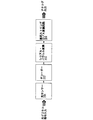
図2にデジタル音声信号をアナログに変換するまでのブロック図を示す。CDプレイヤーなどは光出力を備えているものが多く、このようなものから光ファイバーを通して、光センサー201に光信号を入力する。光センサー201は光信号を電気信号に変換する。この電気信号はEIAJのCP−1201規格などで規定されている。さらにこの信号はデコーダー202によって、図3に示すようなシリアルデジタル音声データにデコードされる。デコードされた電気信号はCDの場合1.411MHzのベースクロックと、44.1KHzのLRクロックとデジタル音声信号データの3種類がある。デジタル音声信号データはMSB(最上位ビット)より順にシリアルに転送される。さらに、シリアルデジタル音声データはシリアルパラレル変換回路203によって、パラレルデジタル音声データとなりD/A変換回路204に入力され、アナログに変換される。
FIG. 2 shows a block diagram until the digital audio signal is converted to analog. Many CD players and the like have an optical output, and an optical signal is input to the optical sensor 201 from such an apparatus through an optical fiber. The optical sensor 201 converts an optical signal into an electrical signal. This electric signal is defined by the CP-1201 standard of EIAJ. Further, this signal is decoded by the decoder 202 into serial digital audio data as shown in FIG. In the case of a CD, there are three types of decoded electrical signals: a 1.411 MHz base clock, a 44.1 KHz LR clock, and digital audio signal data. Digital audio signal data is serially transferred in order from the MSB (most significant bit). Further, the serial digital audio data is converted into parallel digital audio data by the serial / parallel conversion circuit 203 and input to the D /
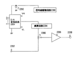
図5に音声信号処理回路の従来例を示す。図5にはD/A変換回路からスピーカー接続部までを記述している。音声信号処理回路はD/A変換回路501、増幅回路506、スピーカー接続部508、D/A変換回路電源502、スイッチ505、アナログ信号入力端子507より構成される。
FIG. 5 shows a conventional example of an audio signal processing circuit. FIG. 5 describes from the D / A conversion circuit to the speaker connection section. The audio signal processing circuit includes a D /
以下、その動作を説明する。パラレルデジタル音声信号はD/A変換回路501によってアナログに変換され、スイッチ505に入力される。一方アナログ音声信号は入力端子507よりスイッチ505に入力される。スイッチ505はD/A変換バッファ回路501の出力もしくはアナログ入力信号を選択し、選択した信号を増幅回路506に入力する。増幅回路506は増幅をおこない、スピーカー接続部508に出力する。
Hereinafter, the operation will be described. The parallel digital audio signal is converted to analog by the D /
ここで利得は例えば以下のようなものとする。アナログ信号入力端子507とD/A変換回路501の出力の信号レベルはいずれも283mVpp、100mVrmsとする。これを増幅回路503で35.3倍に増幅する。すなわちスピーカー接続部には10Vpp、3.54Vrmsの信号が得られる。
Here, for example, the gain is as follows. The signal levels of the analog
従来 の音声信号処理回路ではD/A変換回路は3Vまたは5V系を用いて、図4に示すような、抵抗ストリングを用いたものがあった。
すなわち、複数の抵抗を直列に接続し、抵抗ストリングを形成し、その接続点にスイッチを配置し、そのスイッチを切り換えることにより、求める電圧を得るものである。(例えば特許文献1参照)
Some conventional audio signal processing circuits use a 3V or 5V D / A converter circuit and a resistor string as shown in FIG.
That is, a desired voltage is obtained by connecting a plurality of resistors in series, forming a resistor string, placing a switch at the connection point, and switching the switch. (For example, see Patent Document 1)
以下、図4を用いてその動作を説明する。説明は簡略化のため3ビットを用いて行うが実際の音声信号用のD/A変換回路は10ビット以上が一般的である。まず、端子VHに高電位電源を接続する。また、VLに低電位電源を接続する。端子VHと端子VLの間に7本の抵抗401〜407を直列に接続する。ここで、抵抗401〜407は全て同じ値の抵抗とする。VLを2.3V、VHを3.9Vとすれば各抵抗の両端には0.2Vの電位が発生する。次に各抵抗の接続点にスイッチ408〜415を接続する。さらにスイッチの抵抗と反対側の端子を2つまとめてスイッチ416〜419を接続する。これを繰り返しスイッチ416〜419およびスイッチ420、421を接続する。
The operation will be described below with reference to FIG. The description will be made using 3 bits for simplification, but the actual audio signal D / A converter circuit generally has 10 bits or more. First, a high potential power source is connected to the terminal VH. In addition, a low potential power source is connected to VL. Seven
ここでスイッチの選択をデジタル信号で制御する。すなわち、最下位ビットでスイッチ408〜415を制御し、前述した2組のうちのいずれかを選択する。また、2ビット目のデータでスイッチ416〜419を制御し、2組のうちのいずれかを選択する。また、最上位ビットでスイッチ420、421のいずれかを選択する。このようにして出力端子422には抵抗401〜407の接続点のいずれかが接続される。たとえば、最下位ビットのデータが0であればスイッチ409、411、413、415がオンし、データが1であればスイッチ408、410、412、414がオンするものとする。同様に2ビット目のデータが0であればスイッチ417、419がオンし、データが1であれば416、418がオンするものとする。最上位ビットのデータが0であれば421がオンし、1であれば420がオンするものとする。
Here, the selection of the switch is controlled by a digital signal. That is, the
このような場合でデジタル音声データが111であればスイッチ408、416、420がオンし、VHの電圧3.9Vが出力端子に現れる。また、データが101であればスイッチ410、417、420がオンし、3.5Vの電圧がバッファ回路423を介して出力端子422に現れる。このようにして、デジタル信号をアナログ電圧に変換が可能となる。
In such a case, if the digital audio data is 111, the
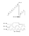
前述したような、抵抗ストリング型D/A変換回路はスイッチで電圧を切り換えるため、スイッチ用トランジスタの容量、一般的にはゲート容量によって、スイッチオフに際して、高電位側または低電位側に引っ張られ、図6に示すようなグリッジが発生する。このようなグリッジはノイズとして感じられるため、音声信号の質を低下させることになる。
例えば、前述したようにアナログ音声信号が100mVrmsであり、D/A変換後のデジタル音声信号も100mVrmsとするとき、グリッジが10mV発生すると、283mVppに対して、28分の1のノイズが発生することになり、S/Nを悪化させることになる。
Since the resistor string type D / A conversion circuit as described above switches the voltage with a switch, it is pulled to the high potential side or the low potential side when the switch is turned off by the capacitance of the switching transistor, generally the gate capacitance, A glitch as shown in FIG. 6 occurs. Since such a glitch is perceived as noise, the quality of the audio signal is degraded.
For example, as described above, when the analog audio signal is 100 mVrms and the digital audio signal after D / A conversion is also 100 mVrms, if a glitch of 10 mV is generated, noise of 1/28 is generated with respect to 283 mVpp. As a result, the S / N is deteriorated.
このようなS/Nの悪化はスピーカーから出力される音声を聞いているユーザーにとって非常に耳障りのものであり、ユーザーに不快感を与えるものであった。 Such deterioration of the S / N is very annoying for the user who is listening to the sound output from the speaker, and is uncomfortable for the user.
以上のような問題を解決するため、本発明はD/A変換回路の電源電圧を表示装置の電源電圧と合わせることにより、D/A変換回路の出力電圧を大きくし、相対的にグリッジの影響を低減するものである。また、音声信号処理回路の利得をアナログ信号入力とデジタル信号入力とで変更するものである。 In order to solve the above problems, the present invention increases the output voltage of the D / A conversion circuit by matching the power supply voltage of the D / A conversion circuit with the power supply voltage of the display device, and relatively affects the glitch. Is reduced. Further, the gain of the audio signal processing circuit is changed between an analog signal input and a digital signal input.
以下に本発明の構成を示す。本発明は絶縁表面上に少なくとも1つの画素と、少なくとも1つのソース信号線と、少なくとも1つのゲート信号線とを有する液晶表示装置において、前記液晶表示装置が、デジタル音声信号をD/A変換するD/A変換回路と、前記ゲート信号線またはソース信号線を駆動する信号線駆動回路と、前記信号線駆動回路と前記D/A変換回路とに同じ電圧を供給する電源回路とを有することを特徴とする。 The configuration of the present invention is shown below. The present invention provides a liquid crystal display device having at least one pixel, at least one source signal line, and at least one gate signal line on an insulating surface, wherein the liquid crystal display device D / A converts a digital audio signal. A D / A converter circuit; a signal line driver circuit that drives the gate signal line or source signal line; and a power supply circuit that supplies the same voltage to the signal line driver circuit and the D / A converter circuit. Features.
本発明の他の構成は、絶縁表面上に少なくとも1つの画素と、少なくとも1つのソース信号線と、少なくとも1つのゲート信号線とを有する液晶表示装置において、前記液晶表示装置が、デジタル音声信号をD/A変換するD/A変換回路と、前記ゲート信号線またはソース信号線を駆動する信号線駆動回路と、前記信号線駆動回路と前記D/A変換回路とに同じ電圧を供給する電源回路と、前記D/A変換回路の出力信号を増幅する増幅回路とを有することを特徴とする。 Another structure of the present invention is a liquid crystal display device having at least one pixel, at least one source signal line, and at least one gate signal line on an insulating surface, wherein the liquid crystal display device outputs a digital audio signal. A D / A conversion circuit for D / A conversion; a signal line drive circuit for driving the gate signal line or source signal line; and a power supply circuit for supplying the same voltage to the signal line drive circuit and the D / A conversion circuit And an amplifying circuit for amplifying the output signal of the D / A conversion circuit.
本発明の他の構成は、絶縁表面上に少なくとも1つの画素と、少なくとも1つのソース信号線と、少なくとも1つのゲート信号線とを有する液晶表示装置において、前記液晶表示装置が、デジタル音声信号をD/A変換するD/A変換回路と、前記ゲート信号線またはソース信号線を駆動する信号線駆動回路と、前記信号線駆動回路と前記D/A変換回路とに同じ電圧を供給する電源回路と、前記D/A変換回路の出力信号を減衰する減衰回路とを有することを特徴とする。 Another structure of the present invention is a liquid crystal display device having at least one pixel, at least one source signal line, and at least one gate signal line on an insulating surface, wherein the liquid crystal display device outputs a digital audio signal. A D / A conversion circuit for D / A conversion; a signal line drive circuit for driving the gate signal line or source signal line; and a power supply circuit for supplying the same voltage to the signal line drive circuit and the D / A conversion circuit And an attenuation circuit for attenuating the output signal of the D / A conversion circuit.
絶本発明の他の構成は、縁表面上に少なくとも1つの画素と、少なくとも1つのソース信号線と、少なくとも1つのゲート信号線とを有する液晶表示装置において、前記液晶表示装置が、デジタル音声信号をD/A変換するD/A変換回路と、前記ゲート信号線またはソース信号線を駆動する信号線駆動回路と、前記信号線駆動回路と前記D/A変換回路とに同じ電圧を供給する電源回路と、前記D/A変換回路によって変換されたアナログ音声信号を含む、複数の異なるアナログ音声信号から信号を選択するスイッチを有していることを特徴とする。 According to another aspect of the present invention, there is provided a liquid crystal display device having at least one pixel, at least one source signal line, and at least one gate signal line on an edge surface, wherein the liquid crystal display device is a digital audio signal. A D / A conversion circuit that performs D / A conversion, a signal line drive circuit that drives the gate signal line or source signal line, and a power source that supplies the same voltage to the signal line drive circuit and the D / A conversion circuit And a switch for selecting a signal from a plurality of different analog audio signals including the analog audio signal converted by the D / A conversion circuit.
本発明の他の構成は、絶縁表面上に少なくとも1つの画素と、少なくとも1つのソース信号線と、少なくとも1つのゲート信号線とを有する液晶表示装置において、前記液晶表示装置が、デジタル音声信号をD/A変換するD/A変換回路と、前記ゲート信号線またはソース信号線を駆動する信号線駆動回路と、前記信号線駆動回路と前記D/A変換回路とに同じ電圧を供給する電源回路と、前記D/A変換回路によって変換されたアナログ音声信号と外部から入力されたアナログ音声信号よりなる、複数の異なるアナログ音声信号から一つを選択するスイッチと、前記スイッチの出力信号を増幅する増幅回路とを有していることを特徴とする。 Another structure of the present invention is a liquid crystal display device having at least one pixel, at least one source signal line, and at least one gate signal line on an insulating surface, wherein the liquid crystal display device outputs a digital audio signal. A D / A conversion circuit for D / A conversion; a signal line drive circuit for driving the gate signal line or source signal line; and a power supply circuit for supplying the same voltage to the signal line drive circuit and the D / A conversion circuit A switch that selects one of a plurality of different analog audio signals, the analog audio signal converted by the D / A conversion circuit and an analog audio signal input from the outside, and an output signal of the switch is amplified And an amplifier circuit.
本発明の他の構成は、絶縁表面上に少なくとも1つの画素と、少なくとも1つのソース信号線と、少なくとも1つのゲート信号線とを有する液晶表示装置において、前記液晶表示装置が、外部から入力されるデジタル音声信号をD/A変換するD/A変換回路と、前記ゲート信号線またはソース信号線を駆動する信号線駆動回路と、前記信号線駆動回路と前記D/A変換回路とに同じ電圧を供給する電源回路と、前記D/A変換回路の出力信号を減衰させる減衰回路と、外部から入力されたアナログ信号または前記減衰回路からの出力信号中から一つを選択するするスイッチとを有していることを特徴とする。 Another structure of the present invention is a liquid crystal display device having at least one pixel, at least one source signal line, and at least one gate signal line on an insulating surface, wherein the liquid crystal display device is inputted from the outside. The same voltage is applied to the D / A conversion circuit that performs D / A conversion of the digital audio signal, the signal line drive circuit that drives the gate signal line or the source signal line, and the signal line drive circuit and the D / A conversion circuit. Power supply circuit, an attenuation circuit for attenuating the output signal of the D / A conversion circuit, and a switch for selecting one of the analog signal input from the outside or the output signal from the attenuation circuit. It is characterized by that.
本発明の他の構成は、絶縁表面上に少なくとも1つの画素と、少なくとも1つのソース信号線と、少なくとも1つのゲート信号線とを有する液晶表示装置において、前記液晶表示装置は、外部から入力されるデジタル音声信号をD/A変換するD/A変換回路と、前記ゲート信号線またはソース信号線を駆動する信号線駆動回路と、前記信号線駆動回路と前記D/A変換回路とに、同じ電圧を供給する電源回路と、外部から入力されるアナログ信号を増幅する増幅回路と、
前記増幅回路の出力信号または前記D/A変換回路の出力信号のいずれか一方を選択するスイッチとを有していることを特徴ている。
Another structure of the present invention is a liquid crystal display device having at least one pixel, at least one source signal line, and at least one gate signal line on an insulating surface, wherein the liquid crystal display device is inputted from the outside. The same applies to a D / A conversion circuit that D / A converts a digital audio signal, a signal line drive circuit that drives the gate signal line or source signal line, and the signal line drive circuit and the D / A conversion circuit. A power supply circuit for supplying voltage, an amplifier circuit for amplifying an analog signal input from the outside,
And a switch for selecting one of the output signal of the amplifier circuit and the output signal of the D / A converter circuit.
本発明の他の構成は、絶縁表面上に少なくとも1つの画素と、少なくとも1つのソース信号線と、少なくとも1つのゲート信号線とを有する液晶表示装置において、前記液晶表示装置は、外部から入力されるデジタル音声信号をD/A変換するD/A変換回路と、前記ゲート信号線またはソース信号線を駆動する信号線駆動回路と、前記信号線駆動回路と前記D/A変換回路とに、同じ電圧を供給する電源回路と、前記D/A変換回路の出力信号を減衰させる減衰回路と、外部から入力されるアナログ信号を増幅する増幅回路と、前記減衰回路の出力信号または前記増幅回路の出力信号のいずれか一方を選択するスイッチとを有していることを特徴としている。 Another structure of the present invention is a liquid crystal display device having at least one pixel, at least one source signal line, and at least one gate signal line on an insulating surface, wherein the liquid crystal display device is inputted from the outside. The same applies to a D / A conversion circuit that D / A converts a digital audio signal, a signal line drive circuit that drives the gate signal line or source signal line, and the signal line drive circuit and the D / A conversion circuit. A power supply circuit that supplies a voltage; an attenuation circuit that attenuates an output signal of the D / A converter circuit; an amplifier circuit that amplifies an analog signal input from the outside; and an output signal of the attenuation circuit or an output of the amplifier circuit And a switch for selecting one of the signals.
本発明の他の構成は、絶縁表面上に少なくとも1つの画素と、少なくとも1つのソース信号線と、少なくとも1つのゲート信号線とを有する液晶表示装置において、前記液晶表示装置が、外部から入力されるデジタル音声信号をD/A変換するD/A変換回路と、前記ゲート信号線またはソース信号線を駆動する信号線駆動回路と、前記信号線駆動回路と前記D/A変換回路とに、同じ電圧を供給する電源回路と、前記D/A変換回路の出力信号を減衰させる減衰回路と、外部から入力されるアナログ信号または前記減衰回路の出力信号のいずれか一方を選択するスイッチと、前記スイッチの出力信号を増幅する増幅回路とを有していることを特徴とした液晶表示装置。 Another structure of the present invention is a liquid crystal display device having at least one pixel, at least one source signal line, and at least one gate signal line on an insulating surface, wherein the liquid crystal display device is inputted from the outside. The same applies to a D / A conversion circuit that D / A converts a digital audio signal, a signal line drive circuit that drives the gate signal line or source signal line, and the signal line drive circuit and the D / A conversion circuit. A power supply circuit that supplies a voltage; an attenuation circuit that attenuates an output signal of the D / A conversion circuit; a switch that selects either an analog signal input from the outside or an output signal of the attenuation circuit; and the switch And an amplifying circuit for amplifying the output signal of the liquid crystal display device.
本発明の他の構成は、絶縁表面上に少なくとも1つの画素と、少なくとも1つのソース信号線と、少なくとも1つのゲート信号線とを有する液晶表示装置において、前記液晶表示装置は、外部から入力されるデジタル音声信号をD/A変換するD/A変換回路と、前記ゲート信号線またはソース信号線を駆動する信号線駆動回路と、前記信号線駆動回路と前記D/A変換回路とに、同じ電圧を供給する電源回路と、外部から入力されるアナログ信号を増幅する第1の増幅回路と、前記第1の増幅回路の出力信号または前記D/A変換回路の出力信号のいずれか一方を選択するスイッチと、前記スイッチの出力信号を増幅する第2の増幅回路を有していることを特徴とした液晶表示装置。 Another structure of the present invention is a liquid crystal display device having at least one pixel, at least one source signal line, and at least one gate signal line on an insulating surface, wherein the liquid crystal display device is inputted from the outside. The same applies to a D / A conversion circuit that D / A converts a digital audio signal, a signal line drive circuit that drives the gate signal line or source signal line, and the signal line drive circuit and the D / A conversion circuit. Select one of a power supply circuit for supplying voltage, a first amplifier circuit for amplifying an analog signal input from the outside, and an output signal of the first amplifier circuit or an output signal of the D / A converter circuit And a second amplifying circuit for amplifying an output signal of the switch.
本発明の他の構成は、絶縁表面上に少なくとも1つの画素と、少なくとも1つのソース信号線と、少なくとも1つのゲート信号線とを有する液晶表示装置において、前記液晶表示装置は、外部から入力されるデジタル音声信号をD/A変換するD/A変換回路と、前記ゲート信号線またはソース信号線を駆動する信号線駆動回路と、前記信号線駆動回路と前記D/A変換回路とに、同じ電圧を供給する電源回路と、前記D/A変換回路の出力信号を減衰させる減衰回路と、外部から入力されるアナログ信号を増幅する第1の増幅回路と、前記第1の増幅回路の出力信号または前記減衰回路の出力信号のいずれか一方を選択するスイッチと、前記スイッチの出力信号を増幅する第2の増幅回路を有していることを特徴としている。 Another structure of the present invention is a liquid crystal display device having at least one pixel, at least one source signal line, and at least one gate signal line on an insulating surface, wherein the liquid crystal display device is inputted from the outside. The same applies to a D / A conversion circuit that D / A converts a digital audio signal, a signal line drive circuit that drives the gate signal line or source signal line, and the signal line drive circuit and the D / A conversion circuit. A power supply circuit that supplies a voltage; an attenuation circuit that attenuates an output signal of the D / A converter circuit; a first amplifier circuit that amplifies an analog signal input from the outside; and an output signal of the first amplifier circuit Alternatively, a switch for selecting one of the output signals of the attenuation circuit and a second amplifier circuit for amplifying the output signal of the switch are provided.
本発明の他の構成は、絶縁表面上に少なくとも1つの画素と、少なくとも1つのソース信号線と、少なくとも1つのゲート信号線とを有する液晶表示装置において、前記液晶表示装置が、外部から入力されるデジタル音声信号をD/A変換するD/A変換回路と、前記ゲート信号線またはソース信号線を駆動する信号線駆動回路と、前記信号線駆動回路と前記D/A変換回路とに、同じ電圧を供給する電源回路と、外部から入力されたアナログ信号または前記D/A変換回路の出力信号のいずれか一方を選択するスイッチと、前記スイッチの出力信号を増幅する増幅回路とを有し、前記増幅回路は前記スイッチの状態に合わせて、利得が変化することを特徴としている。 Another structure of the present invention is a liquid crystal display device having at least one pixel, at least one source signal line, and at least one gate signal line on an insulating surface, wherein the liquid crystal display device is inputted from the outside. The same applies to a D / A conversion circuit that D / A converts a digital audio signal, a signal line drive circuit that drives the gate signal line or source signal line, and the signal line drive circuit and the D / A conversion circuit. A power supply circuit for supplying a voltage, a switch for selecting either an analog signal input from the outside or an output signal of the D / A conversion circuit, and an amplifier circuit for amplifying the output signal of the switch, The amplifying circuit is characterized in that the gain changes in accordance with the state of the switch.
本発明の他の構成は、絶縁表面上に少なくとも1つの画素と、少なくとも1つのソース信号線と、少なくとも1つのゲート信号線とを有する液晶表示装置において、前記液晶表示装置が、外部から入力されるデジタル音声信号をD/A変換するD/A変換回路と、前記ゲート信号線またはソース信号線を駆動する信号線駆動回路と、前記信号線駆動回路と前記D/A変換回路とに、同じ電圧を供給する電源回路と、前記D/A変換回路の出力信号を減衰させる減衰回路と、外部から入力されたアナログ信号または前記減衰回路の出力信号のいずれか一方を選択するスイッチと、前記スイッチの出力信号を増幅する増幅回路とを有し、前記増幅回路は前記スイッチの状態に合わせて、利得が変化することを特徴としたている。 Another structure of the present invention is a liquid crystal display device having at least one pixel, at least one source signal line, and at least one gate signal line on an insulating surface, wherein the liquid crystal display device is inputted from the outside. The same applies to a D / A conversion circuit that D / A converts a digital audio signal, a signal line drive circuit that drives the gate signal line or source signal line, and the signal line drive circuit and the D / A conversion circuit. A power supply circuit that supplies a voltage; an attenuation circuit that attenuates an output signal of the D / A conversion circuit; a switch that selects either an analog signal input from the outside or an output signal of the attenuation circuit; and the switch And an amplifier circuit that amplifies the output signal, wherein the amplifier circuit has a gain that changes in accordance with the state of the switch.
本発明の他の構成は、絶縁表面上に少なくとも1つの画素と、少なくとも1つのソース信号線と、少なくとも1つのゲート信号線とを有する液晶表示装置において、前記液晶表示装置は、外部から入力されるデジタル音声信号をD/A変換するD/A変換回路と、前記ゲート信号線またはソース信号線を駆動する信号線駆動回路と、前記信号線駆動回路と前記D/A変換回路とに、同じ電圧を供給する電源回路と、外部から入力されるアナログ信号を増幅する第1の増幅回路と、前記第1の増幅回路の出力信号または前記D/A変換回路の出力信号のいずれか一方を選択するスイッチと、前記スイッチの出力信号を増幅する第2の増幅回路とを有し、前記第2の増幅回路は前記スイッチの状態に合わせて利得が変化することを特徴としている。 Another structure of the present invention is a liquid crystal display device having at least one pixel, at least one source signal line, and at least one gate signal line on an insulating surface, wherein the liquid crystal display device is inputted from the outside. The same applies to a D / A conversion circuit that D / A converts a digital audio signal, a signal line drive circuit that drives the gate signal line or source signal line, and the signal line drive circuit and the D / A conversion circuit. Select one of a power supply circuit for supplying voltage, a first amplifier circuit for amplifying an analog signal input from the outside, and an output signal of the first amplifier circuit or an output signal of the D / A converter circuit And a second amplifying circuit for amplifying the output signal of the switch, wherein the second amplifying circuit has a gain that changes in accordance with the state of the switch.
本発明の他の構成は、絶縁表面上に少なくとも1つの画素と、少なくとも1つのソース信号線と、少なくとも1つのゲート信号線とを有する液晶表示装置において、前記液晶表示装置は、外部から入力されるデジタル音声信号をD/A変換するD/A変換回路と、前記ゲート信号線またはソース信号線を駆動する信号線駆動回路と、前記信号線駆動回路と前記D/A変換回路とに、同じ電圧を供給する電源回路と、外部から入力されるアナログ信号を増幅する第1の増幅回路と、前記D/A変換回路の出力信号を減衰させる減衰回路と、前記第1の増幅回路の出力信号または前記減衰回路の出力信号のいずれか一方を選択するスイッチと、前記スイッチの出力信号を増幅する第2の増幅回路とを有し、前記第2の増幅回路は前記スイッチの選択状態に合わせて利得が変化することを特徴としている。 Another structure of the present invention is a liquid crystal display device having at least one pixel, at least one source signal line, and at least one gate signal line on an insulating surface, wherein the liquid crystal display device is inputted from the outside. The same applies to a D / A conversion circuit that D / A converts a digital audio signal, a signal line drive circuit that drives the gate signal line or source signal line, and the signal line drive circuit and the D / A conversion circuit. A power supply circuit that supplies a voltage; a first amplifier circuit that amplifies an analog signal input from the outside; an attenuation circuit that attenuates an output signal of the D / A converter circuit; and an output signal of the first amplifier circuit Or a switch that selects one of the output signals of the attenuation circuit, and a second amplifier circuit that amplifies the output signal of the switch, and the second amplifier circuit selects the switch. It is characterized in that the gain is changed according to the state.
本発明の他の構成は、絶縁表面上に少なくとも1つの画素と、少なくとも1つのソース信号線と、少なくとも1つのゲート信号線とを有する液晶表示装置において、前記液晶表示装置は、外部から入力されるデジタル音声信号をD/A変換するD/A変換回路と、前記ゲート信号線またはソース信号線を駆動する信号線駆動回路と、前記信号線駆動回路と前記D/A変換回路とに、同じ電圧を供給する電源回路とを有し、前記D/A変換回路から出力されたアナログ音声信号を含む少なくとも二つのアナログ音声信号の中から、一つを選択して接続を切り換える切り換え回路と、前記少なくとも二つのアナログ音声信号のレベルをそろえるための補正回路を少なくとも一つ備えていることを特徴としている。 Another structure of the present invention is a liquid crystal display device having at least one pixel, at least one source signal line, and at least one gate signal line on an insulating surface, wherein the liquid crystal display device is inputted from the outside. The same applies to a D / A conversion circuit that D / A converts a digital audio signal, a signal line drive circuit that drives the gate signal line or source signal line, and the signal line drive circuit and the D / A conversion circuit. A switching circuit that selects one of the at least two analog audio signals including the analog audio signal output from the D / A conversion circuit and switches the connection; It is characterized by having at least one correction circuit for aligning the levels of at least two analog audio signals.
本発明の他の構成は、上記構成において、前記増幅回路はオペアンプであり、前記利得を変化させる手段は帰還抵抗を切り換えるものであることを特徴としている。 Another configuration of the present invention is characterized in that, in the above configuration, the amplifier circuit is an operational amplifier, and the means for changing the gain switches a feedback resistor.
本発明の他の構成は、上記構成において前記第2の増幅回路はオペアンプであり、前記利得を変化させる手段は帰還抵抗を切り換えるものであることを特徴としている。 Another configuration of the present invention is characterized in that, in the above configuration, the second amplifier circuit is an operational amplifier, and the means for changing the gain switches a feedback resistor.
本発明の他の構成は、上記構成において前記信号線駆動回路およびD/A変換回路は前記絶縁基板上に一体形成されていることを特徴としている。 Another structure of the present invention is characterized in that in the above structure, the signal line driving circuit and the D / A conversion circuit are integrally formed on the insulating substrate.
本発明の他の構成は、上記構成において前記信号線駆動回路およびD/A変換回路は薄膜トランジスタで形成されていることを特徴としている。 Another structure of the present invention is characterized in that in the above structure, the signal line driver circuit and the D / A converter circuit are formed of thin film transistors.
本発明の他の構成は、上記構成において前記D/A変換回路は抵抗ストリング式のD/A変換回路であり、前記抵抗ストリングを構成する抵抗は薄膜半導体を用いたものであることを特徴としている。 Another structure of the present invention is characterized in that, in the above structure, the D / A converter circuit is a resistor string type D / A converter circuit, and the resistor constituting the resistor string uses a thin film semiconductor. Yes.
本発明の他の構成は、上記構成において前記薄膜半導体はその上方または下方に形成される導電体膜との間で容量を形成していることを特徴としている。 Another structure of the present invention is characterized in that in the above structure, the thin film semiconductor forms a capacitance with a conductor film formed above or below the thin film semiconductor.
本発明の他の構成は、上記構成において前記D/A変換回路は抵抗ストリング式のD/A変換回路であり、前記抵抗ストリングを構成する抵抗は金属薄膜を用いたものであることを特徴としている。 Another structure of the present invention is characterized in that, in the above structure, the D / A converter circuit is a resistor string type D / A converter circuit, and the resistor constituting the resistor string uses a metal thin film. Yes.
本発明の他の構成は、上記構成において前記金属薄膜はその上方または下方に形成される導電体膜との間で容量を形成していることを特徴としている。 Another structure of the present invention is characterized in that in the above structure, the metal thin film forms a capacitance with a conductor film formed above or below the metal thin film.
本発明は、上記構成を備える電子機器である。 This invention is an electronic device provided with the said structure.
以上によって、デジタル信号をD/A変換回路で変換しても、グリッジの小さい、S/Nの大きな信号を得ることができる。これにより音質を向上させることが可能となり、より高品質な音声情報を提供できるようになる。 As described above, even if a digital signal is converted by the D / A conversion circuit, a signal having a small glitch and a large S / N can be obtained. As a result, the sound quality can be improved, and higher-quality sound information can be provided.
従来のストリング型D/A変換回路を用いた音声信号処理回路では、トランジスタのオンオフによるグリッジによってS/Nが悪化していた。 In an audio signal processing circuit using a conventional string type D / A conversion circuit, the S / N is deteriorated due to a glitch caused by on / off of a transistor.
本発明は、ストリング型D/A変換回路の電源電圧を表示装置の信号線駆動回路の電源電圧と合わせることによって、出力の振幅を大きくすることができS/Nを改善することが可能となる。また、D/A変換回路の後にある増幅回路利得をアナログ入力とデジタル入力とで切り換えることにより、利得の調整をおこなう。このようにして、それぞれの場合においても良好な振幅を得ることができる。本発明によって、音声出力機能を有する表示装置の音質改良が可能となった。 According to the present invention, the output amplitude can be increased and the S / N can be improved by matching the power supply voltage of the string type D / A converter circuit with the power supply voltage of the signal line driver circuit of the display device. . Further, the gain is adjusted by switching the gain of the amplifier circuit after the D / A conversion circuit between the analog input and the digital input. In this way, a good amplitude can be obtained in each case. According to the present invention, it is possible to improve the sound quality of a display device having an audio output function.
以下、本発明の実施形態を、図面を用いて説明する。 Hereinafter, embodiments of the present invention will be described with reference to the drawings.
(実施形態1)
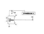
図1は本発明の第1の実施形態を示す図である。第1の実施形態は図1に示すように、D/A変換回路101、D/A変換回路電源102、スピーカー接続部108、信号線駆動回路109により構成される。D/A変換回路101に入力されたデジタル音声信号はアナログ音声信号に変換され、スピーカー接続部108に電気的に接続される。図1においてはスピーカー駆動を前提に表記をおこなっているが、スピーカー接続部は必ずしも必要ではなく、スピーカー接続部は他のものでも良い。
(Embodiment 1)
FIG. 1 is a diagram showing a first embodiment of the present invention. As shown in FIG. 1, the first embodiment includes a D /
第1の実施形態に用いるD/A変換回路は従来例と同じく図4に示すような構成をしているが、D/A変換回路の出力電圧を高くとれるように、D/A変換回路101の電源電圧を表示装置の駆動回路109の電源電圧と同じにしている。
液晶表示装置では少なくとも1つのソース信号線、少なくとも1つのゲート信号線が存在し、それらの交点部分に画素が配置され、ポリシリコンTFTを用いた液晶表示装置などでは、ソース信号線駆動回路、ゲート信号線駆動回路が内蔵されている。一般に、液晶表示装置の信号線駆動回路、特にゲート信号線駆動回路は高い電源電圧、たとえば16V〜20Vが必要である。従って、このような信号線駆動回路と一体化したような音声信号処理装置では、わざわざ高電圧の電源を追加しなくとも、16V〜20Vの電源電圧が使用可能となる。
The D / A converter circuit used in the first embodiment has a configuration as shown in FIG. 4 as in the conventional example. However, the D /
In a liquid crystal display device, at least one source signal line and at least one gate signal line exist, pixels are arranged at intersections thereof, and in a liquid crystal display device using a polysilicon TFT, a source signal line drive circuit, a gate A signal line driver circuit is incorporated. In general, a signal line driving circuit of a liquid crystal display device, particularly a gate signal line driving circuit, requires a high power supply voltage, for example, 16V to 20V. Therefore, in an audio signal processing apparatus integrated with such a signal line driving circuit, a power supply voltage of 16V to 20V can be used without adding a high voltage power supply.
そこで、本発明ではD/A変換回路101の電源電圧を表示装置の信号線駆動回路109の電源電圧と同じとすることとした。例えば、D/A電源102の電源電圧を16Vとすることによって、D/A変換回路101は5V以上の振幅の出力電圧を得ることが可能となる。すなわち、VHを12V、VLを4Vとすれば、D/A変換回路の最大振幅は8Vppとすることができ、従来例と同様に10mV程度のグリッジが発生しても、比率としては1/800に抑えることが可能となる。
Therefore, in the present invention, the power supply voltage of the D /
(実施形態2)
図20は本発明の第2の実施形態を示す図である。第2の実施形態は図20に示すように、D/A変換回路2001、D/A変換回路電源2002、スピーカー接続部2008、信号線駆動回路2009、増幅回路2006により構成される。D/A変換回路2001に入力されたデジタル音声信号はアナログ音声信号に変換される。増幅回路2006はD/A変換回路2001でD/A変換されたアナログ音声信号を増幅する。増幅回路2006はスピーカー接続部2008に電気的に接続される。出力のレベルによっては増幅回路2006を減衰回路とし、アナログ音声信号を減衰して出力してもよい。図20においてはスピーカー駆動を前提に表記をおこなっているが、スピーカー接続部は必ずしも必要ではなく、スピーカー接続部は他のものでも良い。
(Embodiment 2)
FIG. 20 is a diagram showing a second embodiment of the present invention. As shown in FIG. 20, the second embodiment includes a D /
前述した第1の実施形態と同様にD/A変換回路2001の電源を信号線駆動回路2009の電源2002と同じとすることによって、D/A変換回路2001の出力信号の振幅を大きく取ることができ、グリッジの影響を抑えることが可能となる。
As in the first embodiment described above, by making the power supply of the D /
(実施形態3)
図17は本発明の第3の実施形態を示す図である。第3の実施形態は図17に示すように、D/A変換回路1701、D/A変換回路電源1702、スピーカー接続部1708、信号線駆動回路1709、切り換え回路1705、アナログ音声入力部1707により構成される。D/A変換回路1701に入力されたデジタル音声信号はアナログ音声信号に変換される。一方、アナログ音声入力部より別のアナログ音声が入力される。切り換え回路1705はD/A変換回路1701でD/A変換されたアナログ音声信号、またはアナログ音声入力端子1707より入力されたアナログ音声信号のいずれかを選択する。この切り換え回路はスイッチを用いても良い。また、切り換え回路1705はスピーカー接続部1708に電気的に接続される。図17では2つの信号より選択をおこなっているが、選択は2つに限定されず、3つ以上あっても良い。図17においてはスピーカー駆動を前提に表記をおこなっているが、スピーカー接続部は必ずしも必要ではなく、スピーカー接続部は他のものでも良い。
(Embodiment 3)
FIG. 17 is a diagram showing a third embodiment of the present invention. As shown in FIG. 17, the third embodiment includes a D /
前述した第1の実施形態と同様にD/A変換回路1701の電源を信号線駆動回路1709の電源1702と同じとすることによって、D/A変換回路1701の出力信号の振幅を大きく取ることができ、グリッジの影響を抑えることが可能となる。
Similar to the first embodiment described above, by making the power supply of the D /
(実施形態4)
図21は本発明の第4の実施形態を示す図である。第4の実施形態は図21に示すように、D/A変換回路2101、D/A変換回路電源2102、スピーカー接続部2108、信号線駆動回路2109、切り換え回路2105、アナログ音声入力部2107、増幅回路2106により構成される。D/A変換回路2101に入力されたデジタル音声信号はアナログ音声信号に変換される。一方、アナログ音声入力部より別のアナログ音声が入力される。切り換え回路2105はD/A変換回路2101でD/A変換されたアナログ音声信号、またはアナログ音声入力端子2107より入力されたアナログ音声信号のいずれかを選択する。切り換え回路はスイッチを用いても良い。切り換え回路2105は増幅回路2106に接続され、増幅回路2106はアナログ信号を増幅し、また、スピーカー接続部2108に電気的に接続される。図21では2つの信号より選択をおこなっているが、選択は2つに限定されず、3つ以上あっても良い。図21おいてはスピーカー駆動を前提に表記をおこなっているが、スピーカー接続部は必ずしも必要ではなく、スピーカー接続部は他のものでも良い。
(Embodiment 4)
FIG. 21 is a diagram showing a fourth embodiment of the present invention. In the fourth embodiment, as shown in FIG. 21, a D /
前述した第1の実施形態と同様にD/A変換回路2101の電源を信号線駆動回路2109の電源2102と同じとすることによって、D/A変換回路2101の出力信号の振幅を大きく取ることができ、グリッジの影響を抑えることが可能となる。
As in the first embodiment, by making the power supply of the D /
(実施形態5)
図18は本発明の第5の実施形態を示す図である。第5の実施形態は図18に示すように、D/A変換回路1801、D/A変換回路電源1802、スピーカー接続部1808、信号線駆動回路1809、切り換え回路1805、アナログ音声入力部1807、補正回路1804により構成される。D/A変換回路1801に入力されたデジタル音声信号はアナログ音声信号に変換される。一方、アナログ音声入力部1807より別のアナログ音声が入力される。補正回路1804はD/A変換回路1801の出力信号とアナログ信号入力部1807の信号のレベルあわせをおこなう機能を有している。切り換え回路1805は補正回路1804でレベル補正されたアナログ音声信号、またはアナログ音声入力端子1807より入力されたアナログ音声信号のいずれかを選択する。切り換え回路はスイッチを用いても良い。切り換え回路1805はスピーカー接続部1808に電気的に接続される。図18では2つの信号より選択をおこなっているが、選択は2つに限定されず、3つ以上あっても良い。図18おいてはスピーカー駆動を前提に表記をおこなっているが、スピーカー接続部は必ずしも必要ではなく、スピーカー接続部は他のものでも良い。
(Embodiment 5)
FIG. 18 is a diagram showing a fifth embodiment of the present invention. In the fifth embodiment, as shown in FIG. 18, a D /
前述した第1の実施形態と同様にD/A変換回路1801の電源を信号線駆動回路1809の電源1802と同じとすることによって、D/A変換回路1801の出力信号の振幅を大きく取ることができ、グリッジの影響を抑えることが可能となる。
Similar to the first embodiment described above, by making the power supply of the D /
図18では補正回路1804をD/A変換回路1801と切り換え回路1805の間に配置しているが、これには限定されず、アナログ信号入力部1807と切り換え回路1805の間に配置しても良い。また、補正回路をD/A変換回路1801と切り換え回路1805の間と、アナログ信号入力部1807と切り換え回路1805の間の両方に配置しても良い。
In FIG. 18, the correction circuit 1804 is arranged between the D /
(実施形態6)
図19は本発明の第6の実施形態を示す図である。第6の実施形態は図19に示すように、D/A変換回路1901、D/A変換回路電源1902、スピーカー接続部1908、信号線駆動回路1909、切り換え回路1905、アナログ音声入力部1907、補正回路1904、増幅回路1906により構成される。D/A変換回路1901に入力されたデジタル音声信号はアナログ音声信号に変換される。一方、アナログ音声入力部1907より別のアナログ音声が入力される。補正回路1904はD/A変換回路1901の出力信号とアナログ信号入力部1907の信号のレベルあわせをおこなう機能を有している。切り換え回路1905は補正回路1904でレベル補正されたアナログ音声信号、またはアナログ音声入力端子1907より入力されたアナログ音声信号のいずれかを選択する。切り換え回路はスイッチを用いても良い。増幅回路1906は切り換え回路1905の出力信号を増幅する機能を有する。また増幅回路1906はスピーカー接続部1908に電気的に接続される。図19では、切り換え回路1905は2つの信号より選択をおこなっているが、選択信号は2つに限定されず、3つ以上あっても良い。図19おいてはスピーカー駆動を前提に表記をおこなっているが、スピーカー接続部は必ずしも必要ではなく、スピーカー接続部は他のものでも良い。
(Embodiment 6)
FIG. 19 is a diagram showing a sixth embodiment of the present invention. In the sixth embodiment, as shown in FIG. 19, a D /
前述した第1の実施形態と同様にD/A変換回路1901の電源を信号線駆動回路1909の電源1902と同じとすることによって、D/A変換回路1901の出力信号の振幅を大きく取ることができ、グリッジの影響を抑えることが可能となる。
As in the first embodiment described above, by making the power supply of the D /
図19では補正回路1904をD/A変換回路1901と切り換え回路1905の間に配置しているが、これには限定されず、アナログ信号入力部1907と切り換え回路1905の間に配置しても良い。また、補正回路をD/A変換回路1901と切り換え回路1905の間と、アナログ信号入力部1907と切り換え回路1905の間の両方に配置しても良い。
In FIG. 19, the correction circuit 1904 is disposed between the D /
このようにして、上記の実施形態では、D/A変換回路の電源電圧を信号線駆動回路の電源電圧と同じにすることによっての音声信号に対するグリッジのレベルを相対的に下げることができ、D/A変換回路の出力のS/Nを向上させることができ、また、D/A変換回路の出力を減衰することによって、アナログ音声信号のレベル合わせをすることが可能となる。 In this manner, in the above embodiment, the level of the glitch with respect to the audio signal can be relatively lowered by making the power supply voltage of the D / A conversion circuit the same as the power supply voltage of the signal line driving circuit. The S / N of the output of the / A conversion circuit can be improved, and the level of the analog audio signal can be adjusted by attenuating the output of the D / A conversion circuit.
これにより、高品質な音声情報をユーザーに供給することが可能となる。 As a result, high-quality audio information can be supplied to the user.
(実施例1)
図22に本発明の第1の実施例を示す。本実施例は図22に示すように、D/A変換回路2201、D/A変換回路電源2202、減衰回路2204、増幅回路2206、アナログ音声信号入力端子707、デジタルアナログ切り換えスイッチ2205、スピーカー接続部2208より構成される。
以下、従来例と同様にアナログ信号入力端子2207での信号レベル283mVpp、スピーカー接続部2208での信号レベル10Vppを前提に説明をおこなう。
(Example 1)
FIG. 22 shows a first embodiment of the present invention. In this embodiment, as shown in FIG. 22, a D /
The following description will be made assuming that the signal level is 283 mVpp at the analog
本実施例では、実施形態と同じようにD/A変換回路2201の電源電圧を表示装置の信号線駆動回路2209の電源電圧とあわせることにより、高く設定することとした。例えば、D/A変換回路電源2202の電源電圧を16Vとすることによって、D/A変換回路701は5V以上の振幅の出力電圧を得ることが可能となる。すなわち、VHを12V、VLを4Vとすれば、D/A変換回路の最大振幅は8Vppとすることができ、従来例と同様に10mV程度のグリッジが発生しても、比率としては1/800に抑えることが可能となる。
In this example, the power supply voltage of the D /
一方、アナログ音声信号入力端子2207に入力されるアナログ信号は従来例と同じく、283mVppなので、アナログ信号入力時とデジタル信号入力時においてレベルを合わせるために、本実施例において、D/A変換回路の出力信号は減衰回路2204を通過させている。なお、減衰回路2204は音声信号のレベルを合わせるための補正回路の一種である。具体的には減衰回路2204の減衰率を0.035倍に設定すれば、減衰回路2204の出力には283mVppの電圧が出力される。これによって増幅回路2206の入力レベルはアナログ信号入力時、デジタル信号入力時ともに283mVppとなり、増幅回路2206の利得を35.3倍とすれば、スピーカー接続部の出力電圧はアナログ信号入力時、デジタル信号入力時いずれをスイッチ2205で切り換えても10Vpp、約3.5Vrmsとなる。
On the other hand, since the analog signal input to the analog audio
尚、以上述べた利得は一例であり、限定されるものではなく、必要に応じて設定することが可能である。また、たとえば出力電圧が小さくて良い場合は増幅回路2206は用いずともよい。
The gain described above is an example and is not limited, and can be set as necessary. For example, when the output voltage may be small, the
このようにして、本実施例では、D/A変換回路の電源電圧を表示装置の電源電圧と同じにすることによっての音声信号に対するグリッジのレベルを相対的に下げることができ、D/A変換回路の出力のS/Nを向上させることができ、また、アナログ信号のみを増幅することによりアナログ音声信号とのレベル合わせをすることが可能となる。 In this way, in this embodiment, the level of the glitch with respect to the audio signal can be relatively lowered by making the power supply voltage of the D / A conversion circuit the same as the power supply voltage of the display device. The S / N of the output of the circuit can be improved, and the level of the analog audio signal can be adjusted by amplifying only the analog signal.
これにより、高品質な音声情報をユーザーに供給することが可能となる。
(実施例2)
図7に本発明の第2の実施例を示す。本実施例は図7に示すように、D/A変換回路701、D/A変換回路電源702、第1の増幅回路703、第2の増幅回路706、アナログ音声信号入力端子707、デジタルアナログ切り換えスイッチ705、スピーカー接続部708より構成される。
以下、従来例と同様にアナログ信号入力端子707での信号レベル283mVpp、スピーカー接続部708での信号レベル10Vppを前提に説明をおこなう。
As a result, high-quality audio information can be supplied to the user.
(Example 2)
FIG. 7 shows a second embodiment of the present invention. In this embodiment, as shown in FIG. 7, a D /
The following description will be made on the assumption that the signal level at the analog
本実施例では、実施形態と同じようにD/A変換回路701の電源電圧を表示装置の信号線駆動回路709の電源電圧とあわせることにより、高く設定することとした。例えば、D/A変換回路電源702の電源電圧を16Vとすることによって、D/A変換回路701は5V以上の振幅の出力電圧を得ることが可能となる。すなわち、VHを12V、VLを4Vとすれば、D/A変換回路の最大振幅は8Vppとすることができ、従来例と同様に10mV程度のグリッジが発生しても、比率としては1/800に抑えることが可能となる。
In this example, the power supply voltage of the D /
一方、アナログ音声信号入力端子707に入力されるアナログ信号は従来例と同じく、283mVppなので、アナログ信号入力時とデジタル信号入力時においてレベルを合わせるために、本実施例では、アナログ信号のみ第1の増幅回路703を通過させている。なお、増幅回路703は音声信号のレベルを合わせるための補正回路の一種である。具体的には第1の増幅回路703の利得を28.3倍に設定すれば、第1の増幅回路703の出力には8Vの電圧が出力される。これによって第2の増幅回路の入力レベルはアナログ信号入力時、デジタル信号入力時ともに8Vとなり、第2の増幅回路704の利得を1.25倍とすれば、スピーカー接続部の出力電圧はアナログ信号入力時、デジタル信号入力時いずれをスイッチ705で切り換えても10Vpp、約3.5Vrmsとなる。
On the other hand, the analog signal input to the analog audio
尚、以上述べた利得は一例であり、限定されるものではなく、必要に応じて設定することが可能である。また、出力電圧が小さくて良い場合は第2の増幅回路706は用いずともよい。
The gain described above is an example and is not limited, and can be set as necessary. In the case where the output voltage may be small, the
このようにして、本実施例では、D/A変換回路の電源電圧を表示装置の電源電圧と同じにすることによっての音声信号に対するグリッジのレベルを相対的に下げることができ、D/A変換回路の出力のS/Nを向上させることができ、また、アナログ信号のみを増幅することによりアナログ音声信号とのレベル合わせをすることが可能となる。 In this way, in this embodiment, the level of the glitch with respect to the audio signal can be relatively lowered by making the power supply voltage of the D / A conversion circuit the same as the power supply voltage of the display device. The S / N of the output of the circuit can be improved, and the level of the analog audio signal can be adjusted by amplifying only the analog signal.
これにより、高品質な音声情報をユーザーに供給することが可能となる。 As a result, high-quality audio information can be supplied to the user.
(実施例3)
図8に本発明の第3の実施例を示す。本実施例は図8に示すように、D/A変換回路801、D/A変換回路電源802、減衰回路804、第1の増幅回路803、第2の増幅回路806、アナログ音声信号入力端子807、デジタルアナログ切り換えスイッチ805、スピーカー接続部808より構成される。
以下、従来例と同様にアナログ信号入力端子707での信号レベル283mVpp、スピーカー接続部708での信号レベル10Vppを前提に説明をおこなう。
(Example 3)
FIG. 8 shows a third embodiment of the present invention. In this embodiment, as shown in FIG. 8, a D /
The following description will be made on the assumption that the signal level at the analog
本実施例では前記実施形態と同様にD/A変換回路801の電源電圧を表示装置の信号線駆動回路809の電源電圧とあわせることにより、高く設定することとした。例えば、D/A変換回路電源802の電源電圧を16Vとすることによって、D/A変換回路801は5V以上の振幅の出力電圧を得ることが可能となる。すなわち、VHを12V、VLを4Vとすれば、D/A変換回路の最大振幅は8Vppとすることができ、従来例と同様に10mV程度のグリッジが発生しても、比率としては1/800に抑えることが可能となる。
In this example, the power supply voltage of the D /
一方、アナログ音声信号入力端子807に入力されるアナログ信号は従来例と同じく、283mVppなので、アナログ信号入力時とレベルを合わせるためには、デジタル信号入力時の利得を0.0353倍に下げる必要がある。本実施例では、D/A変換回路801の出力を減衰回路804で減衰し、且つアナログ信号を第1の増幅回路803で増幅している。なお、減衰回路804も増幅回路803も音声信号のレベルを合わせるための補正回路の一種である。具体的には減衰回路804の減衰率を0.177とし、第1の増幅回路の利得を5倍とすることによって、アナログ信号入力時、デジタル信号入力時ともに第2の増幅回路806の入力は1.41Vppとなる。第2の増幅回路の利得を7.09倍とすることによって、スピーカー出力端子808での振幅を10Vpp、約3.54Vrmsとすることができる。
On the other hand, the analog signal input to the analog audio
尚、以上述べた利得は一例であり、限定される物ではなく、必要に応じて設定することが可能である。また、出力電圧が小さくて良い場合は第2の増幅回路806は用いずとも良い。
The gain described above is an example and is not limited, and can be set as necessary. When the output voltage may be small, the
このようにして、本実施例では、D/A変換回路の電源電圧を信号線駆動回路の電源電圧と同じにすることによっての音声信号に対するグリッジのレベルを相対的に下げることができ、D/A変換回路の出力のS/Nを向上させることができ、また、D/A変換回路の出力を減衰し、且つアナログ信号増幅回路で増幅したのちスイッチに入力することでアナログ信号入力時とデジタル信号入力時のレベル合わせをすることが可能となる。 In this way, in this embodiment, the level of the glitch relative to the audio signal can be lowered relatively by making the power supply voltage of the D / A conversion circuit the same as the power supply voltage of the signal line drive circuit. The S / N of the output of the A conversion circuit can be improved, and the output of the D / A conversion circuit is attenuated and amplified by the analog signal amplification circuit and then input to the switch, so that the analog signal is input and digital It is possible to adjust the level at the time of signal input.
これにより、高品質な音声情報をユーザーに供給することが可能となる。 As a result, high-quality audio information can be supplied to the user.
(実施例4)
図9に本発明の第4の実施例を示す。本実施例は図9に示すように、D/A変換回路901、D/A電源902、減衰回路904、増幅回路906、アナログ音声信号入力端子907、デジタルアナログ切り換えスイッチ905、スピーカー接続部908より構成される。
以下、従来例と同様にアナログ信号入力端子907での信号レベル283mVpp、スピーカー接続部908での信号レベル10Vppを前提に説明をおこなう。
Example 4
FIG. 9 shows a fourth embodiment of the present invention. As shown in FIG. 9, this embodiment includes a D / A conversion circuit 901, a D / A power source 902, an attenuation circuit 904, an amplification circuit 906, an analog audio signal input terminal 907, a digital / analog changeover switch 905, and a speaker connection unit 908. Composed.
The following description will be made on the assumption that the signal level is 283 mVpp at the analog signal input terminal 907 and the signal level is 10 Vpp at the speaker connection unit 908 as in the conventional example.
そこで、本発明ではD/A変換回路の電源電圧を表示装置の信号線駆動回路の電源電圧とあわせることにより、高く設定することとした。例えば、D/A変換回路電源902の電源電圧を16Vとすることによって、D/A変換回路901は5V以上の振幅の出力電圧を得ることが可能となる。すなわち、VHを12V、VLを4Vとすれば、D/A変換回路の最大振幅は8Vppすることができ、従来例と同様に10mV程度のグリッジが発生しても、比率としては1/800に抑えることが可能となる。 Therefore, in the present invention, the power supply voltage of the D / A conversion circuit is set high by combining it with the power supply voltage of the signal line driving circuit of the display device. For example, by setting the power supply voltage of the D / A conversion circuit power supply 902 to 16 V, the D / A conversion circuit 901 can obtain an output voltage having an amplitude of 5 V or more. That is, if VH is 12 V and VL is 4 V, the maximum amplitude of the D / A converter circuit can be 8 Vpp, and even if a glitch of about 10 mV occurs as in the conventional example, the ratio is 1/800. It becomes possible to suppress.
一方、アナログ音声信号入力端子907に入力されるアナログ信号は従来例と同じく、283mVppなので、アナログ信号入力時とレベルを合わせるためには、デジタル信号入力時の利得を0.0353倍に下げる必要がある。本実施例では以下のような設定をしている。すなわち、D/A変換回路901の出力を減衰回路904で減衰し、且つ増幅回路906の利得をアナログ信号入力時とデジタル信号入力時とで変更する。なお、これら減衰回路、増幅回路は音声信号のレベルを合わせるための補正回路の一種である。 On the other hand, the analog signal input to the analog audio signal input terminal 907 is 283 mVpp as in the conventional example. Therefore, in order to match the level with the analog signal input, it is necessary to reduce the gain when the digital signal is input to 0.0353 times. is there. In this embodiment, the following settings are made. That is, the output of the D / A conversion circuit 901 is attenuated by the attenuation circuit 904, and the gain of the amplification circuit 906 is changed between an analog signal input and a digital signal input. These attenuating circuits and amplifying circuits are a kind of correction circuit for adjusting the level of the audio signal.
具体例としては、減衰回路904の減衰量を0.177とし、増幅回路906の利得をアナログ信号入力時35.4倍、デジタル信号入力時7.09倍とすることによって、アナログ信号入力時とデジタル信号入力時のスピーカー接続部908のレベルいずれも10Vppとすることができる。 As a specific example, the attenuation amount of the attenuation circuit 904 is 0.177, and the gain of the amplification circuit 906 is 35.4 times when an analog signal is input, and 7.09 times when a digital signal is input. The level of the speaker connection portion 908 at the time of digital signal input can be set to 10 Vpp.
尚、以上述べた利得は一例であり、限定されるものではなく、必要に応じて設定することが可能である。また、増幅回路906の取り得る利得範囲が大きいなどの場合は減衰回路904は用いずとも良い。 The gain described above is an example and is not limited, and can be set as necessary. If the gain range that the amplifier circuit 906 can take is large, the attenuation circuit 904 may not be used.
このようにして、本実施例では、D/A変換回路の電源電圧を信号線駆動回路の電源電圧と同じにすることによっての音声信号に対するグリッジのレベルを相対的に下げることができ、D/A変換回路の出力のS/Nを向上させることができ、また、D/A変換回路901の出力を減衰回路904で減衰し、且つ増幅回路906の利得をアナログ信号入力時とデジタル信号入力時とで変更することによりアナログ音声信号とのレベル合わせをすることが可能となる。 In this way, in this embodiment, the level of the glitch relative to the audio signal can be lowered relatively by making the power supply voltage of the D / A conversion circuit the same as the power supply voltage of the signal line drive circuit. The S / N of the output of the A conversion circuit can be improved, the output of the D / A conversion circuit 901 is attenuated by the attenuation circuit 904, and the gain of the amplification circuit 906 is increased when an analog signal is input and when a digital signal is input It is possible to adjust the level with the analog audio signal by changing the above.
これにより、高品質な音声情報をユーザーに供給することが可能となる。 As a result, high-quality audio information can be supplied to the user.
(実施例5)
図10に本発明の第5の実施例を示す。本実施例は図10に示すように、D/A変換回路1001、D/A電源1002、第1の増幅回路1003、第2の増幅回路1006、アナログ音声信号入力端子1007、デジタルアナログ切り換えスイッチ1005、スピーカー接続部1008より構成される。
以下、従来例と同様にアナログ信号入力端子1007での信号レベル283mVpp、スピーカー接続部1008での信号レベル10Vppを前提に説明をおこなう。
(Example 5)
FIG. 10 shows a fifth embodiment of the present invention. In this embodiment, as shown in FIG. 10, a D /
The following description will be made on the assumption that the signal level at the analog
そこで、本発明ではD/A変換回路1001の電源電圧を表示装置の信号線駆動回路1009の電源電圧とあわせることにより、高く設定することとした。例えば、D/A変換回路電源1021の電源電圧を16Vとすることによって、D/A変換回路1001は5V以上の振幅の出力電圧を得ることが可能となる。すなわち、VHを12V、VLを4Vとすれば、D/A変換回路の最大振幅は8Vppすることができ、従来例と同様に10mV程度のグリッジが発生しても、比率としては1/800に抑えることが可能となる。
Therefore, in the present invention, the power supply voltage of the D /
一方、アナログ音声信号入力端子1007に入力されるアナログ信号は従来例と同じく、283mVppなので、アナログ信号入力時とレベルを合わせるためには、アナログ信号入力時、デジタル信号入力時で利得を変える必要がある。本実施例では、アナログ信号のみ第1の増幅回路1003を通過させること、およびアナログ信号入力時とデジタル信号入力時に第2の増幅回路1006の利得を変更することによりレベルを合わせている。なお、この増幅回路は音声信号のレベルを合わせるための補正回路の一種である。
On the other hand, since the analog signal input to the analog audio
具体的には第1の増幅回路1003の利得を5倍に設定すれば、第1の増幅回路1003の出力には1.41Vppの電圧が出力される。アナログ信号入力時における第2の増幅回路の利得を7.09倍に設定する。またデジタル信号入力時における第2の増幅回路の利得を1.25倍に設定すれば、スピーカー接続部の出力電圧はいずれも10Vppとすることができる。尚、以上述べた利得は一例であり、限定されるものではなく、必要に応じて設定することが可能である。
Specifically, when the gain of the
このようにして、本実施例では、D/A変換回路の電源電圧を信号線駆動回路の電源電圧と同じにすることによっての音声信号に対するグリッジのレベルを相対的に下げることができ、D/A変換回路の出力のS/Nを向上させることができ、また、アナログ信号のみを第1の増幅回路で増幅するおよび第2の増幅回路の利得をアナログ信号入力時と、デジタル信号入力時で切り換えることにより、アナログ信号入力時とデジタル信号入力時のスピーカー接続部のレベル合わせをすることが可能となる。 In this way, in this embodiment, the level of the glitch relative to the audio signal can be lowered relatively by making the power supply voltage of the D / A conversion circuit the same as the power supply voltage of the signal line drive circuit. The S / N of the output of the A converter circuit can be improved, and only the analog signal is amplified by the first amplifier circuit, and the gain of the second amplifier circuit is the analog signal input and the digital signal input By switching, it is possible to adjust the level of the speaker connection section when an analog signal is input and when a digital signal is input.
これにより、高品質な音声情報をユーザーに供給することが可能となる。 As a result, high-quality audio information can be supplied to the user.
(実施例6)
図11に本発明の第6の実施例を示す。本実施例は図11に示すように、D/A変換回路1101、D/A電源1102、第1の増幅回路1103、減衰回路1104、第2の増幅回路1106、アナログ音声信号入力端子1107、デジタルアナログ切り換えスイッチ1105、スピーカー接続部1108より構成される。
以下、従来例と同様にアナログ信号入力端子1107での信号レベル283mVpp、スピーカー接続部1108での信号レベル10Vppを前提に説明をおこなう。
(Example 6)
FIG. 11 shows a sixth embodiment of the present invention. In this embodiment, as shown in FIG. 11, a D /
In the following description, the signal level at the analog
そこで、本発明ではD/A変換回路1101の電源電圧を表示装置の信号線駆動回路1109の電源電圧とあわせることにより、高く設定することとした。例えば、D/A変換回路電源1102の電源電圧を16Vとすることによって、D/A変換回路1101は5V以上の振幅の出力電圧を得ることが可能となる。すなわち、VHを12V、VLを4Vとすれば、D/A変換回路の最大振幅は8Vppすることができ、従来例と同様に10mV程度のグリッジが発生しても、比率としては1/800に抑えることが可能となる。
Therefore, in the present invention, the power supply voltage of the D /
一方、アナログ音声信号入力端子1107に入力されるアナログ信号は従来例と同じく、283mVppなので、アナログ信号入力時とレベルを合わせるためには、デジタル信号入力時の利得を0.0353倍に下げる必要がある。本実施例では、アナログ信号のみ第1の増幅回路1103を通過させること、D/A変換回路1101の出力を減衰回路1104で減衰させること、第2の増幅回路1106の利得をアナログ信号入力時とデジタル信号入力時で切り換えることにより、スピーカー接続部1108におけるレベル合わせをおこなっている。
On the other hand, the analog signal input to the analog audio
具体的には第1の増幅回路1103の利得を5倍に設定すれば、第1の増幅回路1003の出力には1.41Vppの電圧が出力される。減衰回路1104の減衰率を0.2に設定し、デジタル信号入力時における第2の増幅回路の利得を6.25倍にすれば、スピーカー接続部1108のレベルは10Vppとなる。また、アナログ信号入力時における第2の増幅回路の利得を7.09倍にすれば、スピーカー接続部におけるレベルは10Vppとなる。このようにして、アナログ信号入力時とデジタル信号入力時のレベルあわせが可能になる。尚、以上述べた利得は一例であり、限定されるものではなく、必要に応じて設定することが可能である。
Specifically, if the gain of the
このようにして、本実施例では、D/A変換回路の電源電圧を信号線駆動回路の電源電圧と同じにすることによっての音声信号に対するグリッジのレベルを相対的に下げることができ、D/A変換回路の出力のS/Nを向上させることができ、また、アナログ信号のみを第1の増幅回路で増幅すること、D/A変換回路出力を減衰回路で減衰すること、第2の増幅回路の利得をアナログ信号入力時とデジタル信号入力時で切り換えることにより、スピーカー接続部におけるアナログ信号入力時とデジタル信号入力時のレベル合わせをすることが可能となる。なお、これら減衰回路、増幅回路は音声信号のレベルを合わせるための補正回路の一種である。 In this way, in this embodiment, the level of the glitch relative to the audio signal can be lowered relatively by making the power supply voltage of the D / A conversion circuit the same as the power supply voltage of the signal line drive circuit. The S / N of the output of the A converter circuit can be improved, and only the analog signal is amplified by the first amplifier circuit, the output of the D / A converter circuit is attenuated by the attenuation circuit, and the second amplification By switching the gain of the circuit between an analog signal input and a digital signal input, it is possible to adjust the level at the time of analog signal input and digital signal input at the speaker connection section. These attenuating circuits and amplifying circuits are a kind of correction circuit for adjusting the level of the audio signal.
これにより、高品質な音声情報をユーザーに供給することが可能となる。 As a result, high-quality audio information can be supplied to the user.
(実施例7)
図14に本発明の第7の実施例を示す。本実施例は、前記実施例をさらに具体的に示したもので、図14に示すように、D/A変換回路1401、D/A電源1402、第1の増幅回路1403、第2の増幅回路1404、第3の増幅回路1405、バッファ増幅回路1106、アナログ音声信号入力端子1407、スピーカー接続部1408、1409、カップリングコンデンサ1410、1412、1413、1414、平滑コンデンサ1411、1415、入力抵抗1416、1420、減衰抵抗1419、利得設定抵抗1417、1418、1421、1422、1423、1424、アナログデジタル切り換えスイッチ1427、バイアス電源1425、1426より構成される。
以下、従来例と同様にアナログ信号入力端子1407での信号レベル283mVpp、スピーカー接続部1408、1409での信号レベル10Vppを前提に説明をおこなう。
(Example 7)
FIG. 14 shows a seventh embodiment of the present invention. This embodiment is a more specific example of the above embodiment. As shown in FIG. 14, a D /
In the following, description will be made on the assumption that the signal level is 283 mVpp at the analog
以下順に動作を説明する。デジタル信号入力時において、D/A変換回路1401の出力はカップリングコンデンサ1413、減衰抵抗1429、切り換えスイッチ1427、カップリングコンデンサ1412を介して、入力抵抗1420、バッファ増幅回路1406に入力される。このとき、信号は減衰抵抗1419と入力抵抗1420で分割されるため、例えば抵抗1419を823kΩ、抵抗1420を177kΩとすると、バッファ増幅回路1406の入力信号レベルは1.41Vppとなる。バッファ増幅回路は利得が1であるため、カップリングコンデンサ1414には1.41Vppの信号が入力される。カップリングコンデンサ1414は抵抗1423、1424、増幅回路1405で構成される反転増幅回路と抵抗1421、1422、増幅回路1404によって構成される非反転増幅回路に入力される。抵抗1423、1424を100kΩ、709kΩとすれば反転増幅回路の利得は7.09倍となる。抵抗1421、1422を100kΩ、609kΩとすれば非反転増幅回路の利得も7.09倍となり、スピーカー接続部1408、1409には約10Vppの出力が得られる。スピーカー接続部1408、1409の出力は互いに逆相であり、BTL駆動をおこなうことができる。尚、ここではスピーカー駆動方式を、BTL駆動前提に説明をおこなったが、BTL駆動に限定されず他の駆動であっても良い。
The operation will be described below in order. When a digital signal is input, the output of the D /
また、アナログ信号入力時には入力端子1407より283mVppのアナログ信号が入力され、カップリングコンデンサ1410を介して、抵抗1416と増幅回路1403に入力される。増幅回路1403の利得は抵抗1417、1418で決まり、抵抗1417を100kΩ、抵抗1418を400kΩとすると増幅回路1403の利得は5倍となり、出力電圧は1.41Vppとなる。増幅回路1403の出力はスイッチ1427、カップリングコンデンサ1412を介して、バッファ増幅回路1406に入力される。その後はデジタル信号入力時と同じである。
When an analog signal is input, an analog signal of 283 mVpp is input from the
このようにして、本実施例では、D/A変換回路の電源電圧を信号線駆動回路の電源電圧と同じにすることによっての音声信号に対するグリッジのレベルを相対的に下げることができ、D/A変換回路の出力のS/Nを向上させることができ、また、アナログ信号のみを第1の増幅回路で増幅すること、D/A変換回路出力を減衰回路で減衰することにより、スピーカー接続部におけるアナログ信号入力時とデジタル信号入力時のレベル合わせをすることが可能となる。 In this way, in this embodiment, the level of the glitch relative to the audio signal can be lowered relatively by making the power supply voltage of the D / A conversion circuit the same as the power supply voltage of the signal line drive circuit. The S / N of the output of the A converter circuit can be improved, and only the analog signal is amplified by the first amplifier circuit, and the output of the D / A converter circuit is attenuated by the attenuation circuit. It is possible to adjust the level when an analog signal is input and when a digital signal is input.
(実施例8)
図15に本発明の第8の実施例を示す。図15(A)は非反転増幅回路であり、入力端子1501、増幅回路1502、出力端子1503、抵抗1504、1505、1507、スイッチ1506によって、構成されている。スイッチ1506が抵抗1504を選択している場合は、増幅回路1502の利得は1+(抵抗1504の抵抗値/抵抗1507の抵抗値)となる。また、スイッチ1506が抵抗1505を選択している場合は、増幅回路1502の利得は1+(抵抗1505の抵抗値/抵抗1507の抵抗値)となる。スイッチ1506を切り換えることにより利得を変更することができる。
(Example 8)
FIG. 15 shows an eighth embodiment of the present invention. FIG. 15A illustrates a non-inverting amplifier circuit which includes an
図15(B)は反転増幅回路であり、入力端子1508、増幅回路1509、出力端子1510、抵抗1511、1512、1514、スイッチ1513によって、構成されている。スイッチ1513が抵抗1511を選択している場合は、増幅回路1509の利得は(抵抗1511の抵抗値/抵抗1514の抵抗値)となる。また、スイッチ1513が抵抗1512を選択している場合は、増幅回路1509の利得は(抵抗1512の抵抗値/抵抗1514の抵抗値)となる。スイッチ1513を切り換えることにより利得を変更することができる。
FIG. 15B illustrates an inverting amplifier circuit which includes an
以上のように帰還抵抗を切り換えるような手段によって、増幅回路の利得を変更することができ、実施例4〜6と組み合わせて使用することができる。尚、利得を変更する手段は本実施例の手段に限定されず、他の手段を用いても良い。 As described above, the gain of the amplifier circuit can be changed by the means for switching the feedback resistor, and can be used in combination with the fourth to sixth embodiments. The means for changing the gain is not limited to the means of this embodiment, and other means may be used.
(実施例9)
図13に本発明の第9の実施例を示す。図13は本発明の抵抗ストリングを用いたD/A変換回路の構造断面図である。抵抗ストリングは図13(B)に示すように蛇行した導体薄膜1301〜1303を抵抗として用い、各接続点にコンタクトホール1304〜1307を配置している。この導体薄膜としては不純物がドープされたシリコンアイランドのような半導体膜、ゲート電極材料、配線などに使用される金属薄膜などが用いられる。本実施例ではこれらの抵抗体の上に絶縁膜1309を介して、導電層を設けている。具体的にはTFTのソース・ドレイン電極相当の導電層1308をかぶせて、抵抗体との間に容量1310を設けている。図13(C)はその断面図である。その等価回路を図13(A)に示す。
このように容量を設けることにより、DA変換回路の電位が安定し、グリッジを低減させることが可能となる。そのため、高品質な音声情報を提供することが可能となる。
本実施例は実施形態1〜6または実施例1〜6と併用することが可能である。
Example 9
FIG. 13 shows a ninth embodiment of the present invention. FIG. 13 is a structural sectional view of a D / A conversion circuit using the resistor string of the present invention. As shown in FIG. 13B, the resistor string uses meandering conductor
By providing the capacitor in this way, the potential of the DA converter circuit is stabilized and glitches can be reduced. Therefore, it is possible to provide high quality audio information.
This example can be used in combination with Embodiments 1 to 6 or Examples 1 to 6.
(実施例10)
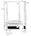
図16に本発明の第10の実施例を示す。図16は本発明を用いた液晶表示装置1601の実施例である。本実施例では、TFT基板1609上に薄膜素子をもちいて、ソース信号線駆動回路1602、ゲート信号線駆動回路1603、画素部1604、音声信号処理回路1605を一体形成し、且つTFT基板1609上に圧電素子型スピーカー1606、FPC1607、1608を実装している。また、対向基板1610とTFT基板1609の間に液晶を挟んでいる。また、基板1609上にTFTで一体形成された音声信号処理回路はD/A変換回路1611、第一の増幅回路1612、スイッチ1613、第2の増幅回路1614を有しているが、構成はこれに限定されない。また、スピーカーは圧電素子型スピーカーに限定されず他のスピーカーでも良い。
(Example 10)
FIG. 16 shows a tenth embodiment of the present invention. FIG. 16 shows an embodiment of a liquid
前述したように、本発明では、ソース信号線駆動回路1602、またはゲート信号線駆動回路1603とD/A変換回路1611の電源を共通化することによって、D/A変換回路1611の出力振幅を大きく取ることが可能となり、デジタル信号入力時のS/Nを向上させることができるため、高品質な音声情報を提供することが可能となる。図16ではD/A変換回路1611とゲート信号線駆動回路1603を電源1615で電圧供給している。図16では電源1605の付近で接続しているが、FPC1607、基板1609の上で接続してもよい。本実施例は実施形態1〜6、実施例1〜9と組み合わせることが可能である。
As described above, in the present invention, the source signal
(実施例11)
以上のようにして作製される表示装置は各種電子機器の表示部として用いることができる。以下に、本発明を用いて形成された表示装置を表示媒体として組み込んだ電子機器について説明する。
(Example 11)
The display device manufactured as described above can be used as a display portion of various electronic devices. Hereinafter, an electronic device in which a display device formed using the present invention is incorporated as a display medium will be described.
その様な電子機器としては、ビデオカメラ、デジタルカメラ、ヘッドマウントディスプレイ(ゴーグル型ディスプレイ)、ゲーム機、カーナビゲーション、パーソナルコンピュータ、携帯情報端末(モバイルコンピュータ、携帯電話または電子書籍等)などが挙げられる。それらの一例を図12に示す。 As such an electronic device, a video camera, a digital camera, a head mounted display (goggles type display), a game machine, a car navigation system, a personal computer, a personal digital assistant (mobile computer, mobile phone, electronic book, etc.), and the like can be given. . An example of them is shown in FIG.
図12(A)はデジタルカメラであり、本体3101、表示部3102、受像部3103、操作キー3104、外部接続ポート3105、シャッター3106等を含む。本発明の表示装置をカメラの表示部3102に用いることで、小型軽量のデジタルカメラを構成することができる。
FIG. 12A illustrates a digital camera, which includes a
図12(B)はノートパソコンであり、本体3201、筐体3202、表示部3203、キーボード3204、外部接続ポート3205、ポインティングマウス3206等を含む。本発明の表示装置を表示部3203に使用することで小型軽量のノートパソコンを構成することができる。
FIG. 12B illustrates a laptop computer, which includes a
図12(C)は携帯情報端末であり、本体3301、表示部3302、スイッチ3303、操作キー3304、赤外線ポート3305等を含む。本発明の表示装置を表示部3302に使用することで、小型軽量な携帯情報端末を構成することができる。
FIG. 12C illustrates a portable information terminal, which includes a
図12(D)は記録媒体を備えた画像再生装置(具体的にはDVD再生装置)であり、本体3401、筐体3402、記録媒体(CD、LDまたはDVD等)読込部3405、操作スイッチ3406、表示部(a)3403、表示部(b)3404等を含む。表示部Aは主として画像情報を表示し、表示部Bは主として文字情報を表示するが、本発明の表示装置は記録媒体を備えた画像再生装置の表示部(a)、(b)に用いることができる。なお、記録媒体を備えた画像再生装置としては、CD再生装置、ゲーム機器などに本発明を用いることで小型軽量な画像再生装置を構成することができる。
FIG. 12D illustrates an image reproduction device (specifically, a DVD reproduction device) including a recording medium, which includes a
図12(E)は折りたたみ式携帯表示装置であり、本体3501に本発明を用いた表示部3502を装着することにより小型軽量な携帯表示装置を構成することができる。
FIG. 12E illustrates a foldable portable display device. By attaching a
図12(F)は腕時計型コミュニケーターであり、本体3601は、表示部3602、操作スイッチ3603などを含む。本発明の表示装置を表示部3602に用いることで小型軽量な腕時計型コミュニケーターを構成することができる。
FIG. 12F illustrates a wristwatch-type communicator. A
図12(G)は携帯電話であり、本体3701は、筐体3702、表示部3703、音声入力部3704、アンテナ3705、操作キー3706、外部接続ポート3707などを含む。本発明の表示装置を表示部3703に用いることで小型軽量な携帯電話を構成することができる。
FIG. 12G illustrates a cellular phone. A
以上の様に、本発明の適用範囲は極めて広く、あらゆる分野の電子機器に適用することが可能である。また、本実施例の電子機器は実施形態1〜6、実施例1〜10のどのような組み合わせからなる構成を用いても実現することができる。 As described above, the application range of the present invention is extremely wide and can be applied to electronic devices in various fields. Moreover, the electronic device of a present Example is realizable even if it uses the structure which consists of what combination of Embodiment 1-6 and Examples 1-10.
Claims (25)
デジタル音声信号をD/A変換するD/A変換回路と、
前記ゲート信号線または前記ソース信号線を駆動する信号線駆動回路と、
前記信号線駆動回路と前記D/A変換回路とに同じ電源電圧を供給する電源回路とを有することを特徴とする液晶表示装置。 And one pixel even without low, at least one source signal line, in a liquid crystal display device having at least one gate signal line,
The digital audio signal and a D / A conversion circuit which converts D / A,
A signal line drive circuit for driving the gate signal line or the source signal line,
A liquid crystal display device comprising: a power supply circuit that supplies the same power supply voltage to the signal line driver circuit and the D / A conversion circuit.
デジタル音声信号をD/A変換するD/A変換回路と、
前記ゲート信号線または前記ソース信号線を駆動する信号線駆動回路と、
前記信号線駆動回路と前記D/A変換回路とに同じ電源電圧を供給する電源回路と、
前記D/A変換回路の出力信号を増幅する増幅回路とを有することを特徴とする液晶表示装置。 And one pixel even without low, at least one source signal line, in a liquid crystal display device having at least one gate signal line,
The digital audio signal and a D / A conversion circuit which converts D / A,
A signal line drive circuit for driving the gate signal line or the source signal line,
A power supply circuit for supplying the same power supply voltage to the signal line driving circuit and the D / A conversion circuit;
A liquid crystal display device comprising: an amplifier circuit for amplifying an output signal of the D / A conversion circuit.
デジタル音声信号をD/A変換するD/A変換回路と、
前記ゲート信号線または前記ソース信号線を駆動する信号線駆動回路と、
前記信号線駆動回路と前記D/A変換回路とに同じ電源電圧を供給する電源回路と、
前記D/A変換回路の出力信号を減衰する減衰回路とを有することを特徴とする液晶表示装置。 And one pixel even without low, at least one source signal line, in a liquid crystal display device having at least one gate signal line,
The digital audio signal and a D / A conversion circuit which converts D / A,
A signal line drive circuit for driving the gate signal line or the source signal line,
A power supply circuit for supplying the same power supply voltage to the signal line driving circuit and the D / A conversion circuit;
A liquid crystal display device comprising: an attenuation circuit that attenuates an output signal of the D / A conversion circuit.
デジタル音声信号をD/A変換するD/A変換回路と、
前記ゲート信号線または前記ソース信号線を駆動する信号線駆動回路と、
前記信号線駆動回路と前記D/A変換回路とに同じ電源電圧を供給する電源回路と、
前記D/A変換回路によって変換されたアナログ音声信号を含む、複数の異なるアナログ音声信号から信号を選択するスイッチとを有することを特徴とする液晶表示装置。 And one pixel even without low, at least one source signal line, in a liquid crystal display device having at least one gate signal line,
The digital audio signal and a D / A conversion circuit which converts D / A,
A signal line drive circuit for driving the gate signal line or the source signal line,
A power supply circuit for supplying the same power supply voltage to the signal line driving circuit and the D / A conversion circuit;
A liquid crystal display device comprising that you have a a switch comprising said analog audio signal converted by the D / A converter circuit selects the signal from a plurality of different analog audio signals.
デジタル音声信号をD/A変換するD/A変換回路と、
前記ゲート信号線または前記ソース信号線を駆動する信号線駆動回路と、
前記信号線駆動回路と前記D/A変換回路とに同じ電源電圧を供給する電源回路と、
前記D/A変換回路によって変換されたアナログ音声信号と外部から入力されたアナログ音声信号よりなる、複数の異なるアナログ音声信号から一つを選択するスイッチと、
前記スイッチの出力信号を増幅する増幅回路とを有することを特徴とする液晶表示装置。 And one pixel even without low, at least one source signal line, in a liquid crystal display device having at least one gate signal line,
The digital audio signal and a D / A conversion circuit which converts D / A,
A signal line drive circuit for driving the gate signal line or the source signal line,
A power supply circuit for supplying the same power supply voltage to the signal line driving circuit and the D / A conversion circuit;
A switch for selecting one of a plurality of different analog audio signals, the analog audio signal converted by the D / A conversion circuit and the analog audio signal input from the outside;
A liquid crystal display device comprising that you have the amplifier circuit for amplifying an output signal of said switch.
外部から入力されるデジタル音声信号をD/A変換するD/A変換回路と、
前記ゲート信号線または前記ソース信号線を駆動する信号線駆動回路と、
前記信号線駆動回路と前記D/A変換回路とに同じ電源電圧を供給する電源回路と、
前記D/A変換回路の出力信号を減衰させる減衰回路と、
外部から入力されたアナログ信号または前記減衰回路からの出力信号のいずれか一方を選択するするスイッチとを有することを特徴とした液晶表示装置。 And one pixel even without low, at least one source signal line, in a liquid crystal display device having at least one gate signal line,
A D / A conversion circuit of the digital audio signal to D / A conversion input from the external,
A signal line drive circuit for driving the gate signal line or the source signal line,
A power supply circuit for supplying the same power supply voltage to the signal line driving circuit and the D / A conversion circuit;
An attenuation circuit for attenuating the output signal of the D / A conversion circuit;
The liquid crystal display device characterized that you have a a switch for selecting either the input analog signal or the output signal from the damping circuit from the outside.
外部から入力されるデジタル音声信号をD/A変換するD/A変換回路と、
前記ゲート信号線または前記ソース信号線を駆動する信号線駆動回路と、
前記信号線駆動回路と前記D/A変換回路とに同じ電源電圧を供給する電源回路と、
外部から入力されるアナログ信号を増幅する増幅回路と、
前記増幅回路の出力信号または前記D/A変換回路の出力信号のいずれか一方を選択するスイッチとを有することを特徴とした液晶表示装置。 And one pixel even without low, at least one source signal line, in a liquid crystal display device having at least one gate signal line,
A D / A conversion circuit of the digital audio signal to D / A conversion input from the external,
A signal line drive circuit for driving the gate signal line or the source signal line,
A power supply circuit for supplying the same supply voltage and the signal line driver circuit and the D / A converter circuit,
An amplifier circuit for amplifying an analog signal input from the outside;
The liquid crystal display device characterized that you have a a switch for selecting either the output signal of the output signal or the D / A conversion circuit of the amplifier circuit.
外部から入力されるデジタル音声信号をD/A変換するD/A変換回路と、
前記ゲート信号線または前記ソース信号線を駆動する信号線駆動回路と、
前記信号線駆動回路と前記D/A変換回路とに同じ電源電圧を供給する電源回路と、
前記D/A変換回路の出力信号を減衰させる減衰回路と、
外部から入力されるアナログ信号を増幅する増幅回路と、
前記減衰回路の出力信号または前記増幅回路の出力信号のいずれか一方を選択するスイッチとを有することを特徴とした液晶表示装置。 And one pixel even without low, at least one source signal line, in a liquid crystal display device having at least one gate signal line,
A D / A conversion circuit of the digital audio signal to D / A conversion input from the external,
A signal line drive circuit for driving the gate signal line or the source signal line,
A power supply circuit for supplying the same supply voltage and the signal line driver circuit and the D / A converter circuit,
An attenuation circuit for attenuating the output signal of the D / A conversion circuit;
An amplifier circuit for amplifying an analog signal input from the outside;
The liquid crystal display device characterized that you have a a switch for selecting either the output signal of the output signal or the amplifier circuit of the damping circuit.
外部から入力されるデジタル音声信号をD/A変換するD/A変換回路と、
前記ゲート信号線または前記ソース信号線を駆動する信号線駆動回路と、
前記信号線駆動回路と前記D/A変換回路とに同じ電源電圧を供給する電源回路と、
前記D/A変換回路の出力信号を減衰させる減衰回路と、
外部から入力されるアナログ信号または前記減衰回路の出力信号のいずれか一方を選択するスイッチと、
前記スイッチの出力信号を増幅する増幅回路とを有することを特徴とした液晶表示装置。 And one pixel even without low, at least one source signal line, in a liquid crystal display device having at least one gate signal line,
A D / A conversion circuit of the digital audio signal to D / A conversion input from the external,
A signal line drive circuit for driving the gate signal line or the source signal line,
A power supply circuit for supplying the same supply voltage and the signal line driver circuit and the D / A converter circuit,
An attenuation circuit for attenuating the output signal of the D / A conversion circuit;
A switch for selecting either an analog signal input from the outside or an output signal of the attenuation circuit;
The liquid crystal display device characterized that you have the amplifier circuit for amplifying an output signal of said switch.
外部から入力されるデジタル音声信号をD/A変換するD/A変換回路と、
前記ゲート信号線または前記ソース信号線を駆動する信号線駆動回路と、
前記信号線駆動回路と前記D/A変換回路とに同じ電源電圧を供給する電源回路と、
外部から入力されるアナログ信号を増幅する第1の増幅回路と、
前記第1の増幅回路の出力信号または前記D/A変換回路の出力信号のいずれか一方を選択するスイッチと、
前記スイッチの出力信号を増幅する第2の増幅回路とを有することを特徴とした液晶表示装置。 And one pixel even without low, at least one source signal line, in a liquid crystal display device having at least one gate signal line,
A D / A conversion circuit of the digital audio signal to D / A conversion input from the external,
A signal line drive circuit for driving the gate signal line or the source signal line,
A power supply circuit for supplying the same supply voltage and the signal line driver circuit and the D / A converter circuit,
A first amplifier circuit for amplifying an analog signal input from the outside;
A switch for selecting either the output signal of the first amplifier circuit or the output signal of the D / A converter circuit;
The liquid crystal display device characterized that you have a second amplifying circuit for amplifying an output signal of said switch.
外部から入力されるデジタル音声信号をD/A変換するD/A変換回路と、
前記ゲート信号線または前記ソース信号線を駆動する信号線駆動回路と、
前記信号線駆動回路と前記D/A変換回路とに同じ電源電圧を供給する電源回路と、
前記D/A変換回路の出力信号を減衰させる減衰回路と、
外部から入力されるアナログ信号を増幅する第1の増幅回路と、
前記第1の増幅回路の出力信号または前記減衰回路の出力信号のいずれか一方を選択するスイッチと、
前記スイッチの出力信号を増幅する第2の増幅回路とを有することを特徴とした液晶表示装置。 And one pixel even without low, at least one source signal line, in a liquid crystal display device having at least one gate signal line,
A D / A conversion circuit of the digital audio signal to D / A conversion input from the external,
A signal line drive circuit for driving the gate signal line or the source signal line,
A power supply circuit for supplying the same supply voltage and the signal line driver circuit and the D / A converter circuit,
An attenuation circuit for attenuating the output signal of the D / A conversion circuit;
A first amplifier circuit for amplifying an analog signal input from the outside;
A switch for selecting either the output signal of the first amplifier circuit or the output signal of the attenuation circuit;
The liquid crystal display device characterized that you have a second amplifying circuit for amplifying an output signal of said switch.
外部から入力されるデジタル音声信号をD/A変換するD/A変換回路と、
前記ゲート信号線または前記ソース信号線を駆動する信号線駆動回路と、
前記信号線駆動回路と前記D/A変換回路とに同じ電源電圧を供給する電源回路と、
外部から入力されたアナログ信号または前記D/A変換回路の出力信号のいずれか一方を選択するスイッチと、
前記スイッチの出力信号を増幅する増幅回路とを有し、
前記増幅回路は前記スイッチの状態に合わせて利得が変化することを特徴とした液晶表示装置。 And one pixel even without low, at least one source signal line, in a liquid crystal display device having at least one gate signal line,
A D / A conversion circuit of the digital audio signal to D / A conversion input from the external,
A signal line drive circuit for driving the gate signal line or the source signal line,
A power supply circuit for supplying the same supply voltage and the signal line driver circuit and the D / A converter circuit,
A switch for selecting either an analog signal input from the outside or an output signal of the D / A converter circuit;
An amplification circuit for amplifying the output signal of the switch,
The liquid crystal display device wherein the amplifier circuit which is characterized in that the gain is changed according to the state of the switch.
外部から入力されるデジタル音声信号をD/A変換するD/A変換回路と、
前記ゲート信号線または前記ソース信号線を駆動する信号線駆動回路と、
前記信号線駆動回路と前記D/A変換回路とに同じ電源電圧を供給する電源回路と、
前記D/A変換回路の出力信号を減衰させる減衰回路と、
外部から入力されたアナログ信号または前記減衰回路の出力信号のいずれか一方を選択するスイッチと、
前記スイッチの出力信号を増幅する増幅回路とを有し、
前記増幅回路は前記スイッチの状態に合わせて利得が変化することを特徴とした液晶表示装置。 And one pixel even without low, at least one source signal line, in a liquid crystal display device having at least one gate signal line,
A D / A conversion circuit of the digital audio signal to D / A conversion input from the external,
A signal line drive circuit for driving the gate signal line or the source signal line,
A power supply circuit for supplying the same supply voltage and the signal line driver circuit and the D / A converter circuit,
An attenuation circuit for attenuating the output signal of the D / A conversion circuit;
A switch for selecting either an analog signal input from the outside or an output signal of the attenuation circuit;
An amplification circuit for amplifying the output signal of the switch,
The liquid crystal display device wherein the amplifier circuit which is characterized in that the gain is changed according to the state of the switch.
外部から入力されるデジタル音声信号をD/A変換するD/A変換回路と、
前記ゲート信号線または前記ソース信号線を駆動する信号線駆動回路と、
前記信号線駆動回路と前記D/A変換回路とに同じ電源電圧を供給する電源回路と、
外部から入力されるアナログ信号を増幅する第1の増幅回路と、
前記第1の増幅回路の出力信号または前記D/A変換回路の出力信号のいずれか一方を選択するスイッチと、
前記スイッチの出力信号を増幅する第2の増幅回路とを有し、
前記第2の増幅回路は前記スイッチの状態に合わせて利得が変化することを特徴とした液晶表示装置。 And one pixel even without low, at least one source signal line, in a liquid crystal display device having at least one gate signal line,
A D / A conversion circuit of the digital audio signal to D / A conversion input from the external,
A signal line drive circuit for driving the gate signal line or the source signal line,
A power supply circuit for supplying the same supply voltage and the signal line driver circuit and the D / A converter circuit,
A first amplifier circuit for amplifying an analog signal input from the outside;
A switch for selecting either the output signal of the first amplifier circuit or the output signal of the D / A converter circuit;
A second amplifier circuit for amplifying the output signal of the switch;
The liquid crystal display device according to claim 2, wherein the gain of the second amplifier circuit changes in accordance with the state of the switch.
外部から入力されるデジタル音声信号をD/A変換するD/A変換回路と、
前記ゲート信号線または前記ソース信号線を駆動する信号線駆動回路と、
前記信号線駆動回路と前記D/A変換回路とに同じ電源電圧を供給する電源回路と、
外部から入力されるアナログ信号を増幅する第1の増幅回路と、
前記D/A変換回路の出力信号を減衰させる減衰回路と、
前記第1の増幅回路の出力信号または前記減衰回路の出力信号のいずれか一方を選択するスイッチと、
前記スイッチの出力信号を増幅する第2の増幅回路とを有し、
前記第2の増幅回路は前記スイッチの選択状態に合わせて利得が変化することを特徴とした液晶表示装置。 And one pixel even without low, at least one source signal line, in a liquid crystal display device having at least one gate signal line,
A D / A conversion circuit for D / A converting a digital audio signal input from the outside;
A signal line drive circuit for driving the gate signal line or the source signal line,
A power supply circuit for supplying the same supply voltage and the signal line driver circuit and the D / A converter circuit,
A first amplifier circuit for amplifying an analog signal input from the outside;
An attenuation circuit for attenuating the output signal of the D / A conversion circuit;
A switch for selecting either the output signal of the first amplifier circuit or the output signal of the attenuation circuit;
A second amplifier circuit for amplifying the output signal of the switch;
The liquid crystal display device, wherein the second amplifier circuit has a gain that changes in accordance with a selection state of the switch.
外部から入力されるデジタル音声信号をD/A変換するD/A変換回路と、
前記ゲート信号線または前記ソース信号線を駆動する信号線駆動回路と、
前記信号線駆動回路と前記D/A変換回路とに同じ電源電圧を供給する電源回路とを有し、
前記D/A変換回路から出力されたアナログ音声信号を含む少なくとも二つのアナログ音声信号の中から、一つを選択して出力する切り換える切り換え回路と、
前記少なくとも二つのアナログ音声信号のレベルをそろえるための補正回路とを有することを特徴とする液晶表示装置。 And one pixel even without low, at least one source signal line, in a liquid crystal display device having at least one gate signal line,
A D / A conversion circuit of the digital audio signal to D / A conversion input from the external,
A signal line drive circuit for driving the gate signal line or the source signal line,
And a power supply circuit for supplying the same supply voltage and the signal line driver circuit and the D / A converter circuit,
A switching circuit for selecting and outputting one of at least two analog audio signals including the analog audio signal output from the D / A conversion circuit;
The liquid crystal display device characterized by having a correction circuit for aligning the level of the at least two analog audio signals.
前記増幅回路はオペアンプであり、帰還抵抗の抵抗値を変化させることによって前記利得を変化させることを特徴とした液晶表示装置。 Oite to claim 12 or claim 1 3,
The amplifier circuit is an operational amplifier, a liquid crystal display device, wherein the benzalkonium changing the gain by changing the resistance value of the feedback resistor.
前記第2の増幅回路はオペアンプであり、帰還抵抗の抵抗値を変化させることによって前記利得を変化させることを特徴とした液晶表示装置。 Oite to claim 14 or claim 1 5,
It said second amplifier circuit is an operational amplifier, a liquid crystal display device, wherein the benzalkonium changing the gain by changing the resistance value of the feedback resistor.
前記信号線駆動回路および前記D/A変換回路は絶縁基板上に一体形成されていることを特徴とした液晶表示装置。 Any Oite to one of claims 1 to 18,
The liquid crystal display device wherein the signal line driving circuit and the D / A converter circuit are integrally formed on the insulation substrate.
前記信号線駆動回路および前記D/A変換回路は薄膜トランジスタを用いて形成されていることを特徴とした液晶表示装置。 Any Oite to one of claims 1 to 19,
The liquid crystal display device wherein the signal line driving circuit and the D / A converter circuit is formed using a thin film transistor.
前記D/A変換回路は抵抗ストリング式のD/A変換回路であり、
前記抵抗ストリング式のD/A変換回路を構成する抵抗は薄膜半導体を用いたものであることを特徴とした液晶表示装置。 Any Oite to one of claims 1 to 20,
The D / A conversion circuit is a resistor string type D / A conversion circuit,
A liquid crystal display device characterized in that the resistor constituting the resistor string type D / A conversion circuit uses a thin film semiconductor.
前記薄膜半導体と、前記薄膜半導体の上方または下方に形成される導電体膜との間で容量を形成していることを特徴とした液晶表示装置。 Oite to claim 2 1,
A liquid crystal display device, wherein a capacitor is formed between the thin film semiconductor and a conductor film formed above or below the thin film semiconductor .
前記D/A変換回路は抵抗ストリング式のD/A変換回路であり、
前記抵抗ストリング式のD/A変換回路を構成する抵抗は金属薄膜を用いたものであることを特徴とした液晶表示装置。 Any Oite to one of claims 1 to 20,
The D / A conversion circuit is a resistor string type D / A conversion circuit,
A resistor constituting the resistor string type D / A conversion circuit is a liquid crystal display device using a metal thin film.
前記金属薄膜と、前記金属薄膜の上方または下方に形成される導電体膜との間で容量を形成していることを特徴とした液晶表示装置。 Oite to claim 2 3,
A liquid crystal display device, wherein a capacitance is formed between the metal thin film and a conductor film formed above or below the metal thin film .
Priority Applications (6)
| Application Number | Priority Date | Filing Date | Title |
|---|---|---|---|
| JP2003285984A JP4130388B2 (en) | 2003-08-04 | 2003-08-04 | Liquid crystal display |
| TW093122133A TWI371734B (en) | 2003-08-04 | 2004-07-23 | Liquid crystal display device and electronic apparatus |
| US10/902,793 US7884788B2 (en) | 2003-08-04 | 2004-08-02 | Liquid crystal display device and electronic apparatus |
| EP04018412A EP1505806A3 (en) | 2003-08-04 | 2004-08-03 | Liquid crystal display device comprising an audio signal processing circuit and electronic apparatus using the same |
| KR1020040061415A KR101077799B1 (en) | 2003-08-04 | 2004-08-04 | Liquid crystal display device and electronic apparatus |
| CNB2004100558315A CN100458531C (en) | 2003-08-04 | 2004-08-04 | Liquid crystal display device and electronic apparatus |
Applications Claiming Priority (1)
| Application Number | Priority Date | Filing Date | Title |
|---|---|---|---|
| JP2003285984A JP4130388B2 (en) | 2003-08-04 | 2003-08-04 | Liquid crystal display |
Publications (3)
| Publication Number | Publication Date |
|---|---|
| JP2005057484A JP2005057484A (en) | 2005-03-03 |
| JP2005057484A5 JP2005057484A5 (en) | 2006-07-20 |
| JP4130388B2 true JP4130388B2 (en) | 2008-08-06 |
Family
ID=33549995
Family Applications (1)
| Application Number | Title | Priority Date | Filing Date |
|---|---|---|---|
| JP2003285984A Expired - Fee Related JP4130388B2 (en) | 2003-08-04 | 2003-08-04 | Liquid crystal display |
Country Status (6)
| Country | Link |
|---|---|
| US (1) | US7884788B2 (en) |
| EP (1) | EP1505806A3 (en) |
| JP (1) | JP4130388B2 (en) |
| KR (1) | KR101077799B1 (en) |
| CN (1) | CN100458531C (en) |
| TW (1) | TWI371734B (en) |
Families Citing this family (9)
| Publication number | Priority date | Publication date | Assignee | Title |
|---|---|---|---|---|
| US7199637B2 (en) * | 2003-09-02 | 2007-04-03 | Semiconductor Energy Laboratory Co., Ltd. | Rectifier circuit without alternating-current feedback |
| US20090051676A1 (en) * | 2007-08-21 | 2009-02-26 | Gyu Hyeong Cho | Driving apparatus for display |
| US20090096816A1 (en) * | 2007-10-16 | 2009-04-16 | Seiko Epson Corporation | Data driver, integrated circuit device, and electronic instrument |
| TWI457673B (en) * | 2011-04-06 | 2014-10-21 | E Ink Holdings Inc | Signal line structure |
| WO2012144234A1 (en) * | 2011-04-21 | 2012-10-26 | パナソニック株式会社 | Voltage generating circuit, analog-digital converter circuit, solid-state image pickup device, and image pickup apparatus |
| CN103733245B (en) * | 2011-07-01 | 2016-04-27 | 矽创电子股份有限公司 | Save the driving circuit of the display panel of circuit area |
| KR101957152B1 (en) * | 2012-05-02 | 2019-06-19 | 엘지디스플레이 주식회사 | Organic light-emitting diode display, circuit and method for driving thereof |
| US9754534B2 (en) | 2015-04-21 | 2017-09-05 | Himax Technologies Limited | Calibrating circuit and calibrating method for display panel |
| KR102359886B1 (en) | 2015-07-07 | 2022-02-09 | 삼성디스플레이 주식회사 | Display panel driving apparatus, method of driving display panel using the same and display apparatus having the same |
Family Cites Families (17)
| Publication number | Priority date | Publication date | Assignee | Title |
|---|---|---|---|---|
| GB8504710D0 (en) * | 1985-02-23 | 1985-03-27 | Plessey Co Plc | Analogue to digital converter |
| JPS6380626A (en) * | 1986-09-24 | 1988-04-11 | Yamaha Corp | Digital/analog converter |
| JPH05157578A (en) * | 1991-12-06 | 1993-06-22 | Rohm Co Ltd | Display control device and level meter |
| US5643804A (en) | 1993-05-21 | 1997-07-01 | Semiconductor Energy Laboratory Co., Ltd. | Method of manufacturing a hybrid integrated circuit component having a laminated body |
| US6954236B1 (en) * | 1993-06-30 | 2005-10-11 | The United States Of America As Represented By The Secretary Of The Navy | Silicon-on-sapphire display with wireless interconnections and method of fabricating same |
| JP3373041B2 (en) * | 1994-05-18 | 2003-02-04 | オリンパス光学工業株式会社 | Image recording device |
| JPH0822024A (en) | 1994-07-05 | 1996-01-23 | Mitsubishi Electric Corp | Active matrix substrate and its production |
| JP2001051292A (en) * | 1998-06-12 | 2001-02-23 | Semiconductor Energy Lab Co Ltd | Semiconductor device and semiconductor display device |
| US6154161A (en) * | 1998-10-07 | 2000-11-28 | Atmel Corporation | Integrated audio mixer |
| JP3088393B2 (en) | 1998-11-04 | 2000-09-18 | 日本電気アイシーマイコンシステム株式会社 | Resistor string type D / A converter |
| JP3403097B2 (en) * | 1998-11-24 | 2003-05-06 | 株式会社東芝 | D / A conversion circuit and liquid crystal display device |
| JP2000244321A (en) | 1999-02-23 | 2000-09-08 | Kokusai Electric Co Ltd | D/a conversion level adjusting device |
| TW521223B (en) | 1999-05-17 | 2003-02-21 | Semiconductor Energy Lab | D/A conversion circuit and semiconductor device |
| KR100360272B1 (en) * | 2000-12-23 | 2002-11-09 | 엘지전자 주식회사 | Azimuth display apparatus and method for image terminal |
| JP2002324845A (en) | 2001-04-26 | 2002-11-08 | Toshiba Corp | Drive circuit for display unit |
| JP2003032333A (en) | 2001-07-12 | 2003-01-31 | Toshiba Corp | Portable terminal |
| US20030097262A1 (en) * | 2001-11-20 | 2003-05-22 | Gateway, Inc. | Handheld device having speech-to text conversion functionality |
-
2003
- 2003-08-04 JP JP2003285984A patent/JP4130388B2/en not_active Expired - Fee Related
-
2004
- 2004-07-23 TW TW093122133A patent/TWI371734B/en not_active IP Right Cessation
- 2004-08-02 US US10/902,793 patent/US7884788B2/en not_active Expired - Fee Related
- 2004-08-03 EP EP04018412A patent/EP1505806A3/en not_active Withdrawn
- 2004-08-04 KR KR1020040061415A patent/KR101077799B1/en not_active IP Right Cessation
- 2004-08-04 CN CNB2004100558315A patent/CN100458531C/en not_active Expired - Fee Related
Also Published As
| Publication number | Publication date |
|---|---|
| TW200509025A (en) | 2005-03-01 |
| CN1580915A (en) | 2005-02-16 |
| KR101077799B1 (en) | 2011-10-31 |
| CN100458531C (en) | 2009-02-04 |
| TWI371734B (en) | 2012-09-01 |
| US7884788B2 (en) | 2011-02-08 |
| JP2005057484A (en) | 2005-03-03 |
| EP1505806A3 (en) | 2008-02-20 |
| US20050030270A1 (en) | 2005-02-10 |
| EP1505806A2 (en) | 2005-02-09 |
| KR20050016138A (en) | 2005-02-21 |
Similar Documents
| Publication | Publication Date | Title |
|---|---|---|
| KR100995481B1 (en) | Display appliance | |
| US10916319B2 (en) | Pulse output circuit, shift register and display device | |
| US7750899B2 (en) | Liquid crystal display device | |
| JP2004173264A (en) | Display device | |
| JP4130388B2 (en) | Liquid crystal display | |
| JP4152797B2 (en) | Active matrix display device | |
| JP4053433B2 (en) | Current output DA converter circuit, display device, and electronic device | |
| JP2004212684A (en) | Electronic circuit and electronic equipment | |
| JP2004236302A (en) | Electronic circuit, display device, and electronic apparatus |
Legal Events
| Date | Code | Title | Description |
|---|---|---|---|
| A521 | Request for written amendment filed |
Free format text: JAPANESE INTERMEDIATE CODE: A523 Effective date: 20060601 |
|
| A621 | Written request for application examination |
Free format text: JAPANESE INTERMEDIATE CODE: A621 Effective date: 20060601 |
|
| A977 | Report on retrieval |
Free format text: JAPANESE INTERMEDIATE CODE: A971007 Effective date: 20080513 |
|
| TRDD | Decision of grant or rejection written | ||
| A01 | Written decision to grant a patent or to grant a registration (utility model) |
Free format text: JAPANESE INTERMEDIATE CODE: A01 Effective date: 20080520 |
|
| A01 | Written decision to grant a patent or to grant a registration (utility model) |
Free format text: JAPANESE INTERMEDIATE CODE: A01 |
|
| A61 | First payment of annual fees (during grant procedure) |
Free format text: JAPANESE INTERMEDIATE CODE: A61 Effective date: 20080521 |
|
| R150 | Certificate of patent or registration of utility model |
Ref document number: 4130388 Country of ref document: JP Free format text: JAPANESE INTERMEDIATE CODE: R150 Free format text: JAPANESE INTERMEDIATE CODE: R150 |
|
| FPAY | Renewal fee payment (event date is renewal date of database) |
Free format text: PAYMENT UNTIL: 20110530 Year of fee payment: 3 |
|
| FPAY | Renewal fee payment (event date is renewal date of database) |
Free format text: PAYMENT UNTIL: 20110530 Year of fee payment: 3 |
|
| FPAY | Renewal fee payment (event date is renewal date of database) |
Free format text: PAYMENT UNTIL: 20110530 Year of fee payment: 3 |
|
| FPAY | Renewal fee payment (event date is renewal date of database) |
Free format text: PAYMENT UNTIL: 20120530 Year of fee payment: 4 |
|
| R250 | Receipt of annual fees |
Free format text: JAPANESE INTERMEDIATE CODE: R250 |
|
| FPAY | Renewal fee payment (event date is renewal date of database) |
Free format text: PAYMENT UNTIL: 20120530 Year of fee payment: 4 |
|
| FPAY | Renewal fee payment (event date is renewal date of database) |
Free format text: PAYMENT UNTIL: 20130530 Year of fee payment: 5 |
|
| R250 | Receipt of annual fees |
Free format text: JAPANESE INTERMEDIATE CODE: R250 |
|
| FPAY | Renewal fee payment (event date is renewal date of database) |
Free format text: PAYMENT UNTIL: 20130530 Year of fee payment: 5 |
|
| R250 | Receipt of annual fees |
Free format text: JAPANESE INTERMEDIATE CODE: R250 |
|
| R250 | Receipt of annual fees |
Free format text: JAPANESE INTERMEDIATE CODE: R250 |
|
| R250 | Receipt of annual fees |
Free format text: JAPANESE INTERMEDIATE CODE: R250 |
|
| R250 | Receipt of annual fees |
Free format text: JAPANESE INTERMEDIATE CODE: R250 |
|
| R250 | Receipt of annual fees |
Free format text: JAPANESE INTERMEDIATE CODE: R250 |
|
| R250 | Receipt of annual fees |
Free format text: JAPANESE INTERMEDIATE CODE: R250 |
|
| R250 | Receipt of annual fees |
Free format text: JAPANESE INTERMEDIATE CODE: R250 |
|
| S531 | Written request for registration of change of domicile |
Free format text: JAPANESE INTERMEDIATE CODE: R313531 |
|
| R350 | Written notification of registration of transfer |
Free format text: JAPANESE INTERMEDIATE CODE: R350 |
|
| LAPS | Cancellation because of no payment of annual fees |