JP4130116B2 - Antistatic mat - Google Patents
Antistatic mat Download PDFInfo
- Publication number
- JP4130116B2 JP4130116B2 JP2002314714A JP2002314714A JP4130116B2 JP 4130116 B2 JP4130116 B2 JP 4130116B2 JP 2002314714 A JP2002314714 A JP 2002314714A JP 2002314714 A JP2002314714 A JP 2002314714A JP 4130116 B2 JP4130116 B2 JP 4130116B2
- Authority
- JP
- Japan
- Prior art keywords
- lattice
- antistatic mat
- forming member
- antistatic
- mat according
- Prior art date
- Legal status (The legal status is an assumption and is not a legal conclusion. Google has not performed a legal analysis and makes no representation as to the accuracy of the status listed.)
- Expired - Fee Related
Links
Images


Classifications
-
- H—ELECTRICITY
- H05—ELECTRIC TECHNIQUES NOT OTHERWISE PROVIDED FOR
- H05F—STATIC ELECTRICITY; NATURALLY-OCCURRING ELECTRICITY
- H05F3/00—Carrying-off electrostatic charges
- H05F3/02—Carrying-off electrostatic charges by means of earthing connections
- H05F3/025—Floors or floor coverings specially adapted for discharging static charges
Description
【0001】
【発明の属する技術分野】
本発明は、主に床上に配設され、静電気を帯電した人や物が載った時に静電気を地面に容易に流すことのできる帯電防止マットに関する。
【0002】
【従来の技術】
近年、静電気を嫌う環境が増加している。例えば、電子部品を扱う工場では静電気を帯びた作業者が触れると、電子部品が損傷することもあり、帯電した作業者の静電気を逃がすことが歩留まり、信頼性の向上のために必要である。そのために、床の上に導電性材料から成る膜を貼り付けることが多い。ところが、このような場合、床はコンクリート製であることが多く、クッション性が悪く、作業者への疲労負荷が大きい。
【0003】
そこで、クッション性を重視した帯電防止マットとして、例えば、特許文献1(特開平9−276205号公報)に記載のマットがある。このマットはモノフィラメントのランダムなループを堆積したものものであって、クッション性はよいがフィラメントの長さが大きいために、充分な帯電防止機能を発揮ができないことがある。また、作業者の足(靴)が踏みつける表面にフィラメントのループが露出しており、歩行しにくく、また、当初はフィラメントのループが厚さ方向に立っていたものが長期間使用している内に倒れて、あるいは寝てしまい、その結果、クッション性も悪化していくという問題があり、また、内部にゴミがたまりやすいという問題もある。
【0004】
【特許文献1】
特開平9−276205号公報
【0005】
【発明が解決しようとする課題】
本発明は上記問題に鑑み、良好な帯電防止機能を有し、クッション性を長期にわたって維持できる帯電防止マットを提供することを目的とする。
【0006】
【課題を解決するための手段】
請求項1の発明によれば、帯電防止マットであって、
弾性を有する導電性材料から成る格子形成部材を略同じ形状の格子穴を多数有するように格子状に配置して形成され、
任意に選択した20mm四方の領域において、格子形成部材の割合が15〜90%であり、
格子形成部材の高さが厚さよりも大きく、且つ作業者の靴が接する格子形成部材の上方の端部が先細に形成されている、
ことを特徴とする帯電防止マットが提供される。
請求項2の発明によれば、請求項1の発明において、格子形成部材の割合が40〜60%であることを特徴とする帯電防止マットが提供される。
請求項3の発明によれば、請求項1の発明において、格子形成部材の下方の端部が平らに形成されていることを特徴とする帯電防止マットが提供される。
請求項4の発明によれば、請求項1の発明において、格子形成部材が、押し出し型のスロットから第1の速度で押し出される直線部材と、隣接する直線部材の間に押し出し型のスロットから第1の速度よりも速い第2の速度で押し出され隣接する直線部材の間で褶曲する波状部材から成ることを特徴とする帯電防止マットが提供される。
請求項5の発明によれば、請求項1の発明において、ハニカム状に格子が形成されていることを特徴とする帯電防止マットが提供される。
請求項6の発明によれば、請求項1の発明において、導電性材料がJIS7215のプラスチックのデュロメータ硬さ試験方法による硬度で40〜70の値を有することを特徴とする帯電防止マットが提供される。
請求項7の発明によれば、請求項1の発明において、導電性材料の漏洩抵抗が10kΩ〜100MΩである、ことを特徴とする帯電防止マットが提供される。
【0007】
【発明の実施の形態】
以下、添付の図面を参照して本発明の実施の形態について説明する。
図1に示されるのは本発明による帯電防止マット1の第1の実施の形態の上面図であって、直線部材11と波状部材12を含む格子形成部材10を有し、隣接する2つの直線部材11の間に波状部材12が挟まれ、直線部材11と波状部材12は互いに結合している。
【0008】
そして、例えば、一つの波状部材12の、図中上方に凸の部分を山とし、図中下方に凸の部分を谷とすると、隣接する2つの山と、これらの山が接する直線部材11の間に(図中上が広い)釣鐘状の格子穴13が形成され、隣接する2つの谷と、これらの谷が接する直線部材11の間には(図中下が広い)釣鐘状の格子穴13が形成されている。
【0009】
帯電防止マット1は約90cm×60cmの大きさを有しているが、任意に選択した20mm四方の領域において、少なくとも1つの、好ましくは、2つ以上の、格子穴13が含まれ、格子形成部材10の割合は、15〜90%とされ、好ましくは40〜60%とされる。 なお、格子形成部材10の割合が、15%以下の場合は上下方向の変形が過大になり、形状を維持することができないし、90%以上の場合は静電気の発生量が大きくなる。
【0010】
ここで、任意に選択した20mm四方の領域において、としているのは、この帯電防止マットは人の足(靴)で踏まれるものであって、例えば、約90cm四方の大きさを有している。したがって、単に、この全体の面積に対して格子形成部材10の割合を規定しただけでは、足(靴)がそのまま全部入るような大きな格子穴ができる可能性があるからである。
【0011】
図2は図1のII-IIに沿って見た波状部材12の断面図であって、上端は図2の(A)に示されるような円弧状、または、(B)に示されるような台形状の、先細な形状とされ、逆に下端は平らにされている。このように、上端を先細にすることによって、静電気の発生がさらに抑制され、下端を平らにすることにより発生した静電気が逃げていきやすい。
【0012】
(A)の場合も、(B)の場合も、厚さt1は0.8〜2.0mm、好ましくは1.0〜1.4mm、より好ましくは1.2mmとされ、高さh1は上記の厚さにした場合に、2〜20mm、好ましくは5〜10mm、より好ましくは7mmとされる。
そして、(A)の場合の上端部の円弧の半径は0.5t〜4tにされ、(B)の場合の台形の高さh’は0.25t〜0.5tとされる。
そして、波の数は直線部材11に波状部材12が5個接する長さWf(図1参照)で規定して、Wf=10mm〜60mm、好ましくは38mmとされる。
【0013】
図3に示すのは図1のIII−III線に沿って見た直線部材11の断面図であって、厚さt2は0.5〜1.5mm、好ましくは0.8mmとされ、高さh2は波状部材12の上端部分を除去した値とされている。したがって、この第1の実施の形態においては、作業者の足(靴)が接するのは波状部材12である。
【0014】
次に、格子形成部材10の材料について説明する。この第1の実施の形態における格子形成部材10の材料は塩化ビニールに導電性の可塑剤を混練したものである。塩化ビニールに混練する導電性の可塑剤はいわゆる界面活性剤であり、界面活性剤を混練することにより樹脂の表面を導電性にするだけでなく表面の摩擦による電荷発生も防止する。
【0015】
この界面活性剤は、イオン性を基準に、アニオン活性剤、カチオン活性剤、両性活性剤、非イオン活性剤の4つに分類される。
塩化ビニールと相性の良いのは、アニオン活性剤のアルキルスルホン酸塩、アカチオン活性剤のアミド型カチオン類、両性活性剤のアルキルベタイン類、非イオン活性剤の脂肪酸モノグリセリド、ソルビタン脂肪酸エステル等がある。
【0016】
塩化ビニール100重量部に対し、導電性可塑剤が80〜180重量部程度添加されるが、さらに、少量の安定剤が追加される。安定剤としては、金属せっけん(高級脂肪酸の金属塩)が用いられるが、金属としては、例えば、Ba(バリウム)/Zn(亜鉛)の2成分がもちいられる。この場合、ZnせっけんはHClの捕捉、アリル塩素との置換をおこない、BaせっけんはHClの捕捉、ZnCl2との配位子交換によるZnせっけんの再生をおこない、ZnCl2とBaせっけんによるZnせっけんの再生がすぐれた安定化効果を発揮する。
【0017】
そして、上記のようにして生成される材料は、JISK7215に規定される「プラスチックのデュロメータ硬さ試験方法」で計測されるデュロメータ硬さが、40〜70、好ましくは55となるようにされる。デュロメータ硬さが40以下であると、上下方向に過大に変形してしまい、70以上であると製品全体の弾力性がなくなり、作業者への負担が過大になってしまう。
【0018】
また、漏洩抵抗が以下の値を有するように導電性可塑剤が混練される。
<加工前の材料(シート状)>
下限値=10kΩ、上限値=100MΩ、好ましくは500kΩ
<第1の実施の形態の形状に加工したもの(SUS板の上に配置)>
下限値=100kΩ、上限値=10MΩ、好ましくは10MΩ
<第1の実施の形態の形状に加工したもの(他の床材の上に配置)>
下限値=100kΩ、上限値=200MΩ、好ましくは25MΩ
いずれもESD STM7.1の試験法による。
なお、下限値以下であると感電のおそれがあり、上限値以上であると静電気が逃げていかない。
【0019】
次に、第1の実施の形態の帯電防止マット10の製造方法について説明する。
第1の実施の形態の帯電防止マット10は、上記のように生成される材料を加熱して溶融状態にし、それを図4に示されるような押し出し型50の出口から押し出して製造される。この押し出し成形は、特公平6−55403号公報に記載されているものであるので簡単に説明する。
【0020】
第1スロット51が直線部材11を形成するためのものであり、第2スロット52が波状部材12を形成するためのものである。第1スロット51は幅が狭いためにここから出てくる材料の速度は低く直線状に出てくる。一方、第2スロット52は幅が広いためにここから出てくる材料の速度は速く、第2スロット52を出て来たものは褶曲し、波状になり、これが、直線部と接合するのである。
【0021】
上記のようにして形成される第1の実施の形態の帯電防止マットの性能について説明する。前述のデュロメータ硬さが55となるようにしたものは良好なクッション性を得ることができ、米国ESD協会 STM97.2の試験法で計測した人体の帯電電位も1V以下であった。
【0022】
次に第2の実施の形態について説明する。図5に示すのが第2の実施の形態の帯電防止マット1を上方から見た図であって、六角形のハニカム格子を有している。
この場合の格子形成部材20の厚さt3は、第1の実施の形態の波状部の厚さt1と同じく、0.8〜2.0mm、好ましくは1.0〜1.4mm、より好ましくは1.2mmとされる。また、高さh3も上記の厚さにした場合に、2〜20mm、好ましくは5〜10mm、より好ましくは7mmとされる。
【0023】
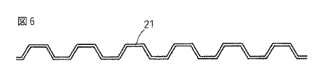
この第2の実施の形態の製造は、第1の実施の形態とは異なり、図6に示すような半割要素21を型で成形し、これを六角形の穴ができるように順次対向配置して、加熱、または、接着剤を用いて、互いに接合することによりおこなう。
あるいは、図7に示すように、六角形の部材22を押し出し成形し、これを、多数束ねて加熱、または、接着剤を用いて、互いに接合し、その後、所定の高さに切断して製造することもできる。
また、図8にシート状の導電材料23に図示のような切れ目24を入れ、その後、切れ目に直角な方向に引っ張ることでも製造することができる。
【0024】
以上、第1の実施の形態で直線部材と波状部材で格子穴が波形になるように格子を形成した場合と、第2の実施の形態で格子穴がハニカム状になるように格子を形成した場合とを説明したが、格子、あるいは、格子穴の形状は、これらに限定されるものではなく、その他の任意の形状にすることができ、例えば、格子穴が四角形になるようにすることも可能である。
【0025】
次に、上記のようにして製造される、本発明の帯電防止マットの使用例について図9を参照して説明する。
図9の(A)は、例えば、タイル、塗り床、長尺シート金属板で導電性の床100が施工されている場合に、その上に置く場合を示し、必要な場所に、本発明による帯電防止マット1を敷くだけでよい。
(B)は通常の非導電性の床100′の上に置く場合を示し、先ず、導電性シート110を非導電性の床100′の上に置き、その上に本発明の帯電防止マット1を敷く。そして、導電性シートを接地処理したものである。導電性シート110は、例えば、導電性樹脂で製造されたものや、あるいは、ステンレス板のような金属板でもよい。あるいは、金属箔を部分的に貼るものでもよい。
(C)は帯電防止マット1に導電性繊維120を織り込み、その繊維を接地したものである。
【0026】
【発明の効果】
各請求項に記載の発明は、帯電防止マットであるが、
弾性を有する導電性材料から成る格子形成部材を略同じ形状の格子穴を多数有するように格子状に配置して形成され、任意に選択した20mm四方の領域において、格子形成部材の割合が15〜90%とされ、格子形成部材の高さが厚さよりも大きく、且つ作業者の靴が接する格子形成部材の上方の端部が先細に形成されており、
良好なクッション性と良好な帯電防止機能を両立する、ことができる。
格子形成部材の割合を、請求項2の発明のように、40〜60%とすると好ましい。
導電性材料の硬さを、請求項6の発明のように、JIS7215のプラスチックのデュロメータ硬さ試験方法による硬度で40〜70の値を有するようにすると好ましい。
導電性材料の漏洩抵抗は、請求項7の発明のように、10kΩ〜100MΩとするのが好ましい。
請求項3の発明のように、格子形成部材の下方の端部を平らに形成すれば静電気が逃げやすい。
請求項4の発明にように、格子形成部材が、押し出し型のスロットから第1の速度で押し出される直線部材と、隣接する直線部材の間に押し出し型のスロットから第1の速度よりも速い第2の速度で押し出され隣接する直線部材の間で褶曲する波状部材から成るようにすれば、押し出し型で容易に製造できる。
【図面の簡単な説明】
【図1】第1の実施の形態の帯電防止マットの上面図である。
【図2】図1のII-II線にそって見た断面図である。
【図3】図1のIII-III線にそって見た断面図である。
【図4】第1の実施の形態の帯電防止マットを製造する型を示す図である。
【図5】第2の実施の形態の帯電防止マットの上面図である。
【図6】第2の実施の形態の一つの製造方法における半割要素を示す図である。
【図7】第2の実施の形態の別の製造方法における六角形断面の要素を示す図である。
【図8】第2の実施の形態のさらに別の製造方法を説明する図である。
【図9】本発明の帯電防止マットの使用例を示す図であって、
(A)は導電性床材の上に置く場合を示し、
(B)は通常の非導電性床材の上に導電性シートを介して置く場合を示し、
(C)は本発明の帯電防止マットに導電性繊維を織り込み、その繊維を接地した場合を示す。
【符号の説明】
1…帯電防止マット
10…格子形成部材
11…直線部材
12…波状部材
13…格子穴
20…格子形成部材
21…半割要素
22…六角形部材
23…シート上導電性材料
24…切れ目
50…押し出し型
51…第1スロット
52…第2スロット
100…導電性の床
100′…非導電性の床
110…導電性シート
120…導電性繊維[0001]
BACKGROUND OF THE INVENTION
The present invention relates to an antistatic mat that is mainly disposed on a floor and can easily flow static electricity to the ground when a person or object charged with static electricity is placed thereon.
[0002]
[Prior art]
In recent years, environments that dislike static electricity have increased. For example, in a factory that handles electronic components, touching by a worker who is charged with static electricity may damage the electronic component, so that it is necessary to release the static electricity of the charged worker and to improve reliability. Therefore, a film made of a conductive material is often stuck on the floor. However, in such a case, the floor is often made of concrete, the cushioning property is poor, and the fatigue load on the worker is large.
[0003]
Therefore, for example, there is a mat described in Patent Document 1 (Japanese Patent Application Laid-Open No. 9-276205) as an antistatic mat with an emphasis on cushioning properties. This mat is obtained by depositing random loops of monofilaments, and has good cushioning properties, but since the filament length is large, it may not be able to exhibit a sufficient antistatic function. In addition, the filament loop is exposed on the surface that the operator's feet (shoes) step on, making it difficult to walk, and the filament loop that originally stood in the thickness direction has been used for a long time. As a result, there is a problem that the cushioning property deteriorates as a result of falling or sleeping, and there is also a problem that dust tends to collect inside.
[0004]
[Patent Document 1]
Japanese Patent Laid-Open No. 9-276205
[Problems to be solved by the invention]
In view of the above problems, an object of the present invention is to provide an antistatic mat having a good antistatic function and capable of maintaining cushioning properties over a long period of time.
[0006]
[Means for Solving the Problems]
According to invention of
It is formed by arranging lattice forming members made of a conductive material having elasticity in a lattice shape so as to have many lattice holes of substantially the same shape,
In 20mm square area arbitrarily selected, the ratio of the lattice forming members Ri 15-90% der,
The height of the grid forming member is larger than the thickness, and the upper end of the grid forming member with which the worker's shoes are in contact is tapered.
An antistatic mat is provided.
According to the second aspect of the present invention, there is provided an antistatic mat according to the first aspect, wherein the ratio of the lattice forming member is 40 to 60%.
According to a third aspect of the present invention, there is provided the antistatic mat according to the first aspect, wherein the lower end of the lattice forming member is formed flat.
According to a fourth aspect of the present invention, in the first aspect of the invention, the lattice forming member is inserted into the linear member that is extruded from the extruded type slot at the first speed and from the extruded type slot between the adjacent linear members. An antistatic mat is provided comprising a corrugated member that is extruded at a second speed greater than one and is curved between adjacent linear members.
According to a fifth aspect of the present invention, there is provided an antistatic mat according to the first aspect, wherein a lattice is formed in a honeycomb shape.
According to a sixth aspect of the present invention, there is provided an antistatic mat according to the first aspect, wherein the conductive material has a hardness value of 40 to 70 according to a JIS7215 plastic durometer hardness test method. The
According to a seventh aspect of the present invention, there is provided an antistatic mat according to the first aspect, wherein the leakage resistance of the conductive material is 10 kΩ to 100 MΩ.
[0007]
DETAILED DESCRIPTION OF THE INVENTION
Hereinafter, embodiments of the present invention will be described with reference to the accompanying drawings.
FIG. 1 is a top view of a first embodiment of an
[0008]
And, for example, if one wave-
[0009]
The
[0010]
Here, in an arbitrarily selected 20 mm square area, the antistatic mat is stepped on a person's foot (shoe), and has a size of about 90 cm square, for example. . Therefore, simply defining the ratio of the
[0011]
FIG. 2 is a cross-sectional view of the
[0012]
In both cases (A) and (B), the thickness t1 is set to 0.8 to 2.0 mm, preferably 1.0 to 1.4 mm, more preferably 1.2 mm, and the height h1 is the above. 2 to 20 mm, preferably 5 to 10 mm, more preferably 7 mm.
The radius of the arc at the upper end in the case of (A) is 0.5t to 4t, and the trapezoidal height h 'in the case of (B) is 0.25t to 0.5t.
The number of waves is defined by a length Wf (see FIG. 1) in which five
[0013]
FIG. 3 is a cross-sectional view of the
[0014]
Next, the material of the
[0015]
This surfactant is classified into four types based on ionicity: an anionic active agent, a cationic active agent, an amphoteric active agent, and a nonionic active agent.
Examples of those having good compatibility with vinyl chloride include an anion activator alkyl sulfonate, an cation activator amide type cation, an amphoteric activator alkyl betaine, a nonionic activator fatty acid monoglyceride, and a sorbitan fatty acid ester.
[0016]
About 80 to 180 parts by weight of a conductive plasticizer is added to 100 parts by weight of vinyl chloride, and a small amount of stabilizer is added. As the stabilizer, metal soap (metal salt of higher fatty acid) is used. As the metal, for example, two components of Ba (barium) / Zn (zinc) are used. In this case, Zn soap captures HCl and displaces allyl chloride, Ba soap captures HCl and regenerates the Zn soap by exchanging ligand with ZnCl 2 and Zn soap by ZnCl 2 and Ba soap It exhibits a stabilizing effect with excellent reproduction.
[0017]
The material generated as described above has a durometer hardness of 40 to 70, preferably 55, as measured by the “plastic durometer hardness test method” defined in JIS K7215. If the durometer hardness is 40 or less, it is excessively deformed in the vertical direction, and if it is 70 or more, the elasticity of the entire product is lost and the burden on the operator becomes excessive.
[0018]
Further, the conductive plasticizer is kneaded so that the leakage resistance has the following value.
<Material before processing (sheet form)>
Lower limit value = 10 kΩ, upper limit value = 100 MΩ, preferably 500 kΩ
<Processed into the shape of the first embodiment (arranged on the SUS plate)>
Lower limit value = 100 kΩ, upper limit value = 10 MΩ, preferably 10 MΩ
<Processed in the shape of the first embodiment (arranged on other flooring)>
Lower limit value = 100 kΩ, upper limit value = 200 MΩ, preferably 25 MΩ
All are based on the test method of ESD STM7.1.
In addition, there exists a possibility of an electric shock if it is below the lower limit, and static electricity does not escape if it is above the upper limit.
[0019]
Next, a method for manufacturing the
The
[0020]
The
[0021]
The performance of the antistatic mat of the first embodiment formed as described above will be described. When the durometer hardness was 55, good cushioning properties were obtained, and the charge potential of the human body measured by the test method of the American ESD Association STM97.2 was 1 V or less.
[0022]
Next, a second embodiment will be described. FIG. 5 is a view of the
In this case, the thickness t3 of the
[0023]
In the manufacture of the second embodiment, unlike the first embodiment, the
Alternatively, as shown in FIG. 7, a
Further, the sheet-like
[0024]
As described above, in the first embodiment, the lattice is formed so that the lattice holes are corrugated by the linear member and the corrugated member, and in the second embodiment, the lattice is formed so that the lattice holes are honeycomb-shaped. However, the shape of the lattice or the lattice hole is not limited to these, and may be any other shape. For example, the lattice hole may be square. Is possible.
[0025]
Next, an example of use of the antistatic mat of the present invention produced as described above will be described with reference to FIG.
FIG. 9A shows, for example, a case where the
(B) shows a case where it is placed on a normal
(C) is one in which
[0026]
【The invention's effect】
The invention described in each claim is an antistatic mat,
It is formed by arranging lattice forming members made of an electrically conductive material having elasticity in a lattice shape so as to have many lattice holes of substantially the same shape, and the ratio of the lattice forming members is 15 to 15 in an arbitrarily selected 20 mm square region. 90%, the height of the grid forming member is larger than the thickness, and the upper end of the grid forming member that comes into contact with the shoe of the worker is tapered,
It is possible to achieve both good cushioning properties and a good antistatic function.
The ratio of the lattice forming member is preferably 40 to 60% as in the invention of claim 2.
It is preferable that the hardness of the conductive material has a value of 40 to 70 according to the JIS7215 plastic durometer hardness test method as in the invention of claim 6 .
The leakage resistance of the conductive material is preferably 10 kΩ to 100 MΩ as in the invention of
If the lower end portion of the lattice forming member is formed flat as in the invention of claim 3 , static electricity can easily escape.
According to a fourth aspect of the present invention, the lattice forming member has a linear member extruded at a first speed from the extrusion type slot and a first speed higher than the first speed from the extrusion type slot between the adjacent linear members. If it is made of a wave-like member that is extruded at a speed of 2 and bends between adjacent linear members, it can be easily manufactured with an extrusion die.
[Brief description of the drawings]
FIG. 1 is a top view of an antistatic mat according to a first embodiment.
FIG. 2 is a cross-sectional view taken along line II-II in FIG.
3 is a cross-sectional view taken along line III-III in FIG.
FIG. 4 is a view showing a mold for manufacturing the antistatic mat of the first embodiment.
FIG. 5 is a top view of an antistatic mat according to a second embodiment.
FIG. 6 is a diagram showing a halved element in one manufacturing method of the second embodiment.
FIG. 7 is a diagram showing elements having a hexagonal cross section in another manufacturing method according to the second embodiment;
FIG. 8 is a diagram illustrating still another manufacturing method according to the second embodiment.
FIG. 9 is a view showing an example of use of the antistatic mat of the present invention,
(A) shows the case where it puts on the conductive flooring,
(B) shows the case where it puts via a conductive sheet on a normal non-conductive flooring,
(C) shows a case where conductive fibers are woven into the antistatic mat of the present invention and the fibers are grounded.
[Explanation of symbols]
DESCRIPTION OF
Claims (7)
弾性を有する導電性材料から成る格子形成部材を略同じ形状の格子穴を多数有するように格子状に配置して形成され、
任意に選択した20mm四方の領域において、格子形成部材の割合が15〜90%であり、
格子形成部材の高さが厚さよりも大きく、且つ作業者の靴が接する格子形成部材の上方の端部が先細に形成されている、
ことを特徴とする帯電防止マット。An antistatic mat,
It is formed by arranging lattice forming members made of a conductive material having elasticity in a lattice shape so as to have many lattice holes of substantially the same shape,
In 20mm square area arbitrarily selected, the ratio of the lattice forming member Ri 15-90% der,
The height of the grid forming member is larger than the thickness, and the upper end of the grid forming member with which the shoe of the worker is in contact is tapered,
An antistatic mat characterized by that.
Priority Applications (3)
| Application Number | Priority Date | Filing Date | Title |
|---|---|---|---|
| JP2002314714A JP4130116B2 (en) | 2002-10-29 | 2002-10-29 | Antistatic mat |
| AU2003267154A AU2003267154A1 (en) | 2002-10-29 | 2003-09-11 | Antistatic mat |
| PCT/US2003/028648 WO2004039217A2 (en) | 2002-10-29 | 2003-09-11 | Antistatic mat |
Applications Claiming Priority (1)
| Application Number | Priority Date | Filing Date | Title |
|---|---|---|---|
| JP2002314714A JP4130116B2 (en) | 2002-10-29 | 2002-10-29 | Antistatic mat |
Publications (2)
| Publication Number | Publication Date |
|---|---|
| JP2004147780A JP2004147780A (en) | 2004-05-27 |
| JP4130116B2 true JP4130116B2 (en) | 2008-08-06 |
Family
ID=32211622
Family Applications (1)
| Application Number | Title | Priority Date | Filing Date |
|---|---|---|---|
| JP2002314714A Expired - Fee Related JP4130116B2 (en) | 2002-10-29 | 2002-10-29 | Antistatic mat |
Country Status (3)
| Country | Link |
|---|---|
| JP (1) | JP4130116B2 (en) |
| AU (1) | AU2003267154A1 (en) |
| WO (1) | WO2004039217A2 (en) |
Families Citing this family (3)
| Publication number | Priority date | Publication date | Assignee | Title |
|---|---|---|---|---|
| JP2006023119A (en) * | 2004-07-06 | 2006-01-26 | Fab Solution Kk | Method and device for evaluating electrostatic discharge damage preventing material |
| US8163701B2 (en) | 2005-08-19 | 2012-04-24 | Signature Therapeutics, Inc. | Prodrugs of active agents |
| KR100785320B1 (en) | 2006-10-26 | 2007-12-17 | 유동헌 | Footboard for cleaning shoes |
Family Cites Families (4)
| Publication number | Priority date | Publication date | Assignee | Title |
|---|---|---|---|---|
| US4981544A (en) * | 1989-02-03 | 1991-01-01 | Minnesota Mining And Manufacturing Company | Static dissipative tape |
| JP3288759B2 (en) | 1992-08-12 | 2002-06-04 | 日立ビアメカニクス株式会社 | Dust collector for printed circuit board processing machine |
| JPH09276205A (en) | 1996-04-15 | 1997-10-28 | Towa:Kk | Conductive, antistatic mat |
| DE29706847U1 (en) * | 1997-04-16 | 1997-08-07 | Abel Winfried | Doormat |
-
2002
- 2002-10-29 JP JP2002314714A patent/JP4130116B2/en not_active Expired - Fee Related
-
2003
- 2003-09-11 WO PCT/US2003/028648 patent/WO2004039217A2/en active Application Filing
- 2003-09-11 AU AU2003267154A patent/AU2003267154A1/en not_active Abandoned
Also Published As
| Publication number | Publication date |
|---|---|
| WO2004039217A3 (en) | 2004-07-08 |
| AU2003267154A8 (en) | 2004-05-25 |
| JP2004147780A (en) | 2004-05-27 |
| WO2004039217A2 (en) | 2004-05-13 |
| AU2003267154A1 (en) | 2004-05-25 |
Similar Documents
| Publication | Publication Date | Title |
|---|---|---|
| EP1116450A2 (en) | Mold-in fastening member and production of molded resin article having mold-in fastening member | |
| JP2006506123A (en) | Mat with elastic and compressible elements | |
| CN101028164B (en) | Ground pad installing parts | |
| AU736729B2 (en) | Female member of mechanical fastener | |
| JP4130116B2 (en) | Antistatic mat | |
| EP1070470A1 (en) | Structural unit having net member incorporated therein, seat and method for treating end section of net member | |
| JP5300229B2 (en) | Carpet and method for manufacturing carpet | |
| JP2007138653A (en) | Hard tile which engages projection and notch and manufacturing method therefor | |
| CN202112411U (en) | Double-density conductive shoes | |
| JP4277017B2 (en) | Work mat | |
| JP3073734U (en) | Fiber molding material | |
| JP4825922B1 (en) | Manufacturing method of non-slip mat | |
| US10369909B2 (en) | Surface fastener, cushioning structure, and seat structure | |
| CN219438776U (en) | Detachable floor mat | |
| JP7149581B2 (en) | Belt brushes, cleaners and washers | |
| CN219544230U (en) | Soft bottom carpet | |
| JP6074354B2 (en) | Dust scattering prevention floor mat | |
| CN215127010U (en) | Rubber cushion | |
| JP3154904U (en) | mattress | |
| JPH0249680Y2 (en) | ||
| KR20130080101A (en) | 3d mesh and the bedding thereof | |
| JPH09195485A (en) | Tatami border | |
| TWM474052U (en) | Quick assembling part of floor mat | |
| JPH0124136Y2 (en) | ||
| JPH0595465U (en) | Dust control mat |
Legal Events
| Date | Code | Title | Description |
|---|---|---|---|
| A621 | Written request for application examination |
Free format text: JAPANESE INTERMEDIATE CODE: A621 Effective date: 20050914 |
|
| A131 | Notification of reasons for refusal |
Free format text: JAPANESE INTERMEDIATE CODE: A131 Effective date: 20080108 |
|
| A521 | Written amendment |
Free format text: JAPANESE INTERMEDIATE CODE: A523 Effective date: 20080325 |
|
| TRDD | Decision of grant or rejection written | ||
| A01 | Written decision to grant a patent or to grant a registration (utility model) |
Free format text: JAPANESE INTERMEDIATE CODE: A01 Effective date: 20080422 |
|
| A01 | Written decision to grant a patent or to grant a registration (utility model) |
Free format text: JAPANESE INTERMEDIATE CODE: A01 |
|
| A61 | First payment of annual fees (during grant procedure) |
Free format text: JAPANESE INTERMEDIATE CODE: A61 Effective date: 20080520 |
|
| R150 | Certificate of patent or registration of utility model |
Free format text: JAPANESE INTERMEDIATE CODE: R150 |
|
| FPAY | Renewal fee payment (event date is renewal date of database) |
Free format text: PAYMENT UNTIL: 20110530 Year of fee payment: 3 |
|
| FPAY | Renewal fee payment (event date is renewal date of database) |
Free format text: PAYMENT UNTIL: 20110530 Year of fee payment: 3 |
|
| FPAY | Renewal fee payment (event date is renewal date of database) |
Free format text: PAYMENT UNTIL: 20120530 Year of fee payment: 4 |
|
| FPAY | Renewal fee payment (event date is renewal date of database) |
Free format text: PAYMENT UNTIL: 20130530 Year of fee payment: 5 |
|
| FPAY | Renewal fee payment (event date is renewal date of database) |
Free format text: PAYMENT UNTIL: 20130530 Year of fee payment: 5 |
|
| R250 | Receipt of annual fees |
Free format text: JAPANESE INTERMEDIATE CODE: R250 |
|
| LAPS | Cancellation because of no payment of annual fees |