JP4129724B2 - Liquid crystal display device and electronic apparatus using the same - Google Patents
Liquid crystal display device and electronic apparatus using the same Download PDFInfo
- Publication number
- JP4129724B2 JP4129724B2 JP2002174518A JP2002174518A JP4129724B2 JP 4129724 B2 JP4129724 B2 JP 4129724B2 JP 2002174518 A JP2002174518 A JP 2002174518A JP 2002174518 A JP2002174518 A JP 2002174518A JP 4129724 B2 JP4129724 B2 JP 4129724B2
- Authority
- JP
- Japan
- Prior art keywords
- liquid crystal
- polarizing plate
- substrate
- display device
- layer
- Prior art date
- Legal status (The legal status is an assumption and is not a legal conclusion. Google has not performed a legal analysis and makes no representation as to the accuracy of the status listed.)
- Expired - Fee Related
Links
Images


Landscapes
- Polarising Elements (AREA)
- Liquid Crystal (AREA)
Description
【0001】
【発明の属する技術分野】
本発明は、液晶表示装置および電子機器に関し、特に、半透過反射型の液晶表示装置であって、反射モードのみならず、透過モード時にも十分に明るい表示が可能な液晶表示装置の構成に関するものである。
【0002】
【従来の技術】
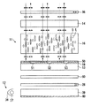
従来から、明るい場所では、通常の反射型の液晶表示装置と同様に外光を利用し、暗い場所では、内部の光源により表示を視認可能にした液晶表示装置が提案されている。この液晶表示装置は、反射モードと透過モードを兼ね備えた表示方式を採用しており、周囲の明るさに応じていずれかの表示方式に切り替えることにより、消費電力を低減しつつ周囲が暗い場合でも明瞭な表示を行うことができる。以下、本明細書では、この種の液晶表示装置のことを「半透過反射型液晶表示装置」という。半透過反射型液晶表示装置の一形態として、アルミニウム等の金属膜に光透過用の開口部を形成した反射膜を下基板の内面に備え、この反射膜を半透過反射膜として機能させるものが提案されている。なお、本明細書では液晶表示装置を構成する各基板の液晶側の面を「内面」、それと反対側の面を「外面」という。
【0003】
図16は、この種の半透過反射膜を用いた半透過反射型液晶表示装置の一例を示している。
この液晶表示装置100では、一対のガラス基板101,102間に液晶層103が挟持されており、下基板101の内面に、開口部104aを有する半透過反射層104、透明電極108、配向膜107が形成されている。一方、上基板102の内面には、透明電極112、配向膜113が形成されている。
【0004】
また、上基板102の外面側には、2枚の位相差板118、119(これら位相差板は1/4波長板120として機能する)、上偏光板114が配置され、下基板101の外面側には、1/4波長板115、下偏光板116が設けられている。さらに、光源122、導光板123、反射板124等からなるバックライト117が下偏光板116の下方に配置されている。なお、1/4波長板115,120は、ある波長帯域において直線偏光をほぼ円偏光にすることができるものである。
【0005】
図16に示す半透過反射型液晶表示装置100の表示原理を以下、図17を用いて説明する。なお、図17では、図11の液晶表示装置の構成要素のうち、表示原理の説明に必要なものだけを図示している。
まず、暗表示を行う場合には、液晶層103に電圧を印加して(オン状態として)液晶層103での位相差がない状態としておく。反射表示においては、上偏光板114の上方から入射した光は、上偏光板114の透過軸を紙面に垂直とすると、上偏光板114を透過した後、紙面に垂直な直線偏光となり、さらに1/4波長板120を透過した後、左回りの円偏光となり、液晶層103を透過する。そして、半透過反射層104の表面で反射すると回転方向が反転して右回りの円偏光となり、液晶層103を透過し、1/4波長板120を透過した後、紙面に平行な直線偏光となる。ここで、上偏光板114は紙面に垂直な透過軸を有しているので、反射光は上偏光板114に吸収されて外部(観察者側)へは戻らず、暗表示となる。
【0006】
一方、透過表示においては、バックライト117から出射された光は、下偏光板116の透過軸を紙面に平行とした場合、下偏光板116を透過した後、紙面に平行な直線偏光となり、さらに1/4波長板115を透過した後、右回りの円偏光となり、液晶層103を透過する。そして、右回りの円偏光が1/4波長板120を透過した後、紙面に平行な直線偏光となり、反射モードと同様、上偏光板114に吸収されて暗表示となる。
【0007】
次に、明表示を行う場合には、液晶層103に電圧を印加しない状態(オフ状態)とし、このときの液晶層103での複屈折効果による位相差が1/4波長になるように設定しておく。反射表示においては、上偏光板114の上方から入射し、上偏光板114、1/4波長板120を透過した後の左回りの円偏光は、液晶層103を透過して半透過反射層104の表面に到達した段階で紙面に平行な直線偏光となる。そして、半透過反射層104の表面で反射して液晶層103を透過すると、再度左回りの円偏光となり、1/4波長板120を透過した後、紙面に垂直な直線偏光となる。ここで、上偏光板114は紙面に垂直な透過軸を有しているので、反射光は上偏光板114を透過して外部(観察者側)へ戻り、明表示となる。
【0008】
一方、透過表示においては、バックライト117から入射し、下偏光板116、1/4波長板115を透過した後の右回りの円偏光は、液晶層103を透過した段階で紙面に垂直な直線偏光となる。そして、紙面に垂直な直線偏光が1/4波長板120を透過すると左回りの円偏光となり、上偏光板114は紙面に垂直な透過軸を有しているので、左回りの円偏光のうち、紙面に垂直な直線偏光のみが上偏光板114を透過して明表示となる。
【0009】
【発明が解決しようとする課題】
このように、図16、図17に示す液晶表示装置100によれば、外光の有無に関わらず表示の視認が可能ではあるものの、反射表示に比べて透過表示の明るさが不足するという問題があった。
その原因の一つは、図17による表示原理の説明で述べたように、透過表示で明表示を行う場合、液晶層103、1/4波長板120を透過して上偏光板114に入射される光が円偏光となっているので、その円偏光の略半分の光が上偏光板114で吸収されてしまい、表示に寄与しないからである。
【0010】
また、他の原因の一つは、バックライト117から出射された光のうち、半透過反射層104の開口部104aを通過せず、半透過反射層104の裏面で反射した光は、回転方向が反転して左回りの円偏光となり、1/4波長板115を透過すると紙面に垂直な直線偏光になる。そして、この直線偏光が紙面に平行な透過軸を有する下偏光板116によって吸収されることになる。つまり、バックライト117から出射された光のうち、開口部104aを通過しなかった光が、仮に下偏光板116に吸収されることなく下偏光板116を透過してバックライト117まで戻ってくれば、この戻り光が再度液晶セルに向けて出射されるが、実際には半透過反射層104の裏面で反射した後、下偏光板116によってほぼ全てが吸収されてしまい、再利用できないからである。
【0011】
ところで、二色性色素を添加した液晶、いわゆるゲストホスト液晶については良く知られている。このゲストホスト液晶を半透過反射型液晶表示装置に用いた場合、反射表示部では光が液晶層を2回通過するのに対して、透過表示部においては光が液晶層を通過するのは1回だけであるので、二色性色素による光の吸収量が反射表示部と透過表示部とで異なる。したがって、透過表示で充分なコントラストが得られるように色素濃度を調整すると、非常に反射率の低い反射表示しか得られない。逆に、反射表示で充分な明るさと適正なコントラストが得られるように色素濃度を調整すると、透過表示においては非常に低いコントラストになってしまうという問題があった。
【0012】
このようにゲストホスト液晶を半透過反射型液晶表示装置に適用した場合、反射表示と透過表示の双方で良好な光学特性を得るのは困難であった。この問題点を解決する手法が特開平11−242226号公報に開示されているが、この手法では反射表示部と透過表示部とで同時刻の液晶の配向状態を異ならせることが必須であり、そのために装置構成が複雑で製造も困難であるという欠点を有している。
【0013】
本発明は、上記の課題を解決するためになされたものであって、反射表示と透過表示の双方が可能な半透過反射型の液晶表示装置において、双方の表示モードにおける表示特性を向上させ、透過表示において高いコントラストが得られる液晶表示装置を提供することを目的とする。また、本発明は、反射表示と透過表示の双方の表示モードにおける表示特性を向上させ、透過表示におけるコントラストを高めた液晶表示部を備えた電子機器を提供することを目的とする。
【0014】
【課題を解決するための手段】
上記の目的を達成するために、本発明の液晶表示装置は、互いに対向する一対の基板の間に液晶層が挟持され、1つのドット領域内に透過表示領域と反射表示領域とを有する半透過反射型の液晶表示装置であって、前記一対の基板の一方の基板の外面側に第1偏光板が設けられるとともに前記一対の基板の他方の基板の外面側に第2偏光板が設けられ、前記第2偏光板と前記他方の基板との間に、前記液晶層の旋光による波長分散を補償又は緩和するとともに、前記第2偏光板から入射された直線偏光の偏光方向を前記他方の基板の内面に近接する液晶分子の配向方向に概ね垂直な方向に変換する位相補償層が設けられ、前記液晶層は、二色性色素が混入された誘電異方性が正の液晶組成物を含み、前記液晶層の液晶分子は、前記一対の基板の間において基板面に平行な面内で略90°ねじれており、前記第1偏光板の透過軸方向と前記一方の基板の内面に近接する液晶分子の配向方向とは概ね平行であることを特徴とする。
【0015】
この構成の透過モードにおける暗表示時の作用について、図2を用いて説明する。図2は本発明の原理を説明するための図であり、二色性色素Sを含んだ液晶層16が上下の基板14,13で挟持され、各基板14,13の外面側にそれぞれ偏光板36,28が設けられるとともに、下基板13の内面側に半透過反射層18が形成された半透過反射型の液晶表示装置を模式的に示している。
ここで、液晶層16の液晶分子Lは、非選択電圧印加時に上基板14と下基板13との間において基板面に平行な面内で略90°ねじれており、上基板14の内面側に接する液晶分子Lの配向方向は上偏光板(第1偏光板)36の透過軸に略平行となっている。また、比較のために、この液晶表示装置を位相補償層を設けない左側部分と、位相補償層60を下基板13と下偏光板28との間に介装させた右側部分とに分けているが、各下偏光板(第2偏光板)28の透過軸は下基板13の内面側に接する液晶分子Lの配向方向に対して適宜の角度に配され、液晶層16に入射する光の偏光方向が上記配向方向に概ね垂直となるようになっている。
【0016】
本構成によれば、透過表示において、下偏光板28を透過して直線偏光となった光は、位相補償層60により、その偏光方向が下基板28の内面に接する液晶分子Lの配向方向と概ね垂直となるように変換される(図2の右側部分参照)。そして、この光は液晶層16を透過すると、その偏光方向は、90°回転されて上偏光板36の透過軸と概ね垂直となる。
また、上記の光は、液晶層16を透過する前に予め液晶層16の旋光による波長分散を補償又は緩和する方向に位相がずらされるため、上偏光板36に到達した際の光のトータルの位相のずれ量は位相補償層60がない場合(図2の左側部分参照)に比べて小さくなる。その結果、上偏光板36に到達した上記の光の偏光状態は、位相補償層60がない場合に比べて直線偏光に近くなり、光抜けが防止されて良好な暗表示となる。
【0017】
理想的には、可視光の広い波長範囲に亘って液晶の旋光性による波長分散が完全に補償されるようにすることで、図2の右側部分に示したように、上偏光板に到達したR,G,Bの光の全てが楕円偏光成分を全く含まない直線偏光となり、出射光量をゼロとすることができる。これにより、暗表示における光抜けを効果的に抑えることができ、透過表示におけるコントラストを向上させることができる。
【0018】
また、図示を省略するが、本構成では、反射表示では液晶による旋光性と二色性色素Sによる光吸収とを利用しているため、色素濃度を調節することで、このような色素の光吸収を利用して表示を行なう反射表示と、光の旋光性のみを利用する透過表示との双方の表示特性を同時に向上することができる。また、透過表示に円偏光を用いないため、明表示時に上偏光板で吸収される成分がなく、透過表示を明るくすることができる。さらに、本発明の液晶表示装置においては、透過表示部と反射表示部の同時刻における液晶の配向状態は基本的に同じでよく、複雑な構成を必要としない。
【0019】
また、本発明の液晶表示装置は、互いに対向する一対の基板の間に液晶層が挟持され、1つのドット領域内に透過表示領域と反射表示領域とを有する半透過反射型の液晶表示装置であって、前記一対の基板の一方の基板の外面側に第1偏光板が設けられるとともに前記一対の基板の他方の基板の外面側に第2偏光板が設けられ、前記第2偏光板と前記他方の基板との間に、前記液晶層の旋光による波長分散を補償又は緩和するとともに、前記第2偏光板から入射された直線偏光(波長λ)に対して概ねλの位相差を形成し該直線偏光の偏光状態を保持する位相補償層が設けられ、前記液晶層は、二色性色素が混入された誘電異方性が正の液晶組成物を含み、前記液晶層の液晶分子は、前記一対の基板の間において基板面に平行な面内で略90°ねじれており、前記第1偏光板の透過軸方向と前記第1基板の内面に近接する液晶分子の配向方向とは概ね平行であり、前記第2偏光板の透過軸方向と前記他方の基板の内面に近接する液晶分子の配向方向とは概ね垂直であることを特徴とする。
【0020】
すなわち、本構成は、下偏光板の透過軸を下基板の内面に接する液晶分子の配向方向と概ね垂直とするとともに、位相補償層によって形成される位相差を概ねλとして下偏光板から入射される直線偏光の偏光状態を保持するようにしたものである。本構成によっても、下偏光板から液晶層内に入射する光を、その偏光方向が下基板の内面に接する液晶分子の配向方向に概ね垂直で、且つ、その位相が液晶の旋光性による波長分散が補償又は緩和される方向にずれた状態とすることができる。そのため、上述したのと同様の作用効果を奏し、透過表示のコントラストを向上させることができる。
【0021】
さらに、本発明の液晶表示装置は、互いに対向する一対の基板の間に液晶層が挟持され、1つのドット領域内に透過表示領域と反射表示領域とを有する半透過反射型の液晶表示装置であって、前記一対の基板の一方の基板の外面側に第1偏光板が設けられるとともに前記一対の基板の他方の基板の外面側に第2偏光板が設けられ、前記第2偏光板と前記他方の基板との間に、前記液晶層の旋光による波長分散を補償又は緩和するとともに、前記第2偏光板から入射された直線偏光(波長λ)に対して概ねλ/2の位相差を形成する位相補償層が設けられ、前記液晶層は、二色性色素が混入された誘電異方性が正の液晶組成物を含み、前記液晶層の液晶分子は、前記一対の基板の間において基板面に平行な面内で略90°ねじれており、前記第1偏光板の透過軸方向と前記一方の基板の内面に近接する液晶分子の配向方向とは概ね平行であり、前記位相補償層の遅相軸と前記他方の基板の内面に近接する液晶分子の配向方向とのなす角度がθであり、前記第2偏光板の透過軸と前記他方の基板の内面に接する液晶分子の配向方向とのなす角度が概ね2θであることを特徴とする。
【0022】
この構成によれば、透過表示において、下偏光板を透過して直線偏光となった光は、位相補償層によってその偏光方向が2θだけ回転されるため、下基板に到達した際に、その偏光方向が下基板の内面に接する液晶分子の配向方向に概ね垂直となる。したがって、本構成でも上述したのと同様の作用効果を奏し、透過表示のコントラストを向上させることができる。
【0023】
なお、上記のθの値は略45°であることが望ましい。この構成によれば、透過表示において、下偏光板を透過して直線偏光となった光は位相補償層を透過すると、偏光面が略90°回転された直線偏光となる。そして、この直線偏光の内、半透過反射層の裏面で反射された光は位相補償層を透過して再度偏光面を90°回転され、下偏光板に戻される。この際、この直線偏光の偏光方向と下偏光板の透過軸とは平行であるため、この直線偏光は下偏光板をそのまま透過する。このため、半透過反射層で反射された光を再利用して透過表示に寄与させることができ、明るい表示が可能となる。
【0024】
また、位相補償層を半透過反射層よりも外面側に配置することが好ましい。この構成によれば、反射表示において輝度が低下することがなく明るい表示が得られる。勿論、位相補償層を透過表示領域にのみ設けてもよい。この構成によっても反射表示の輝度を低下させることはない。
また、前記液晶層のリタデーション値Δnd(Δn:屈折率異方性,d:液晶層厚)が、Δnd=0.866・λ(λ:380nm〜780nm)を満たすように構成してもよい。この構成によれば、反射表示において階調反転のない高い表示品質を得ることができる。なお、Δnd=0.866・λとすべき根拠については、[発明の実施の形態]の項で後述する。
【0025】
位相補償層を、複数の位相差板の組み合わせとして構成してもよい。この構成によれば、液晶層に対して位相補償層のリタデーションを合わせこむ際の部材選択の自由度が高まる。
なお、上基板と下基板との間にカラーフィルタを設けてもよい。この構成によれば、反射表示、透過表示の双方で明瞭なカラー表示が可能な液晶表示装置を実現することができる。
本発明の電子機器は、上記本発明の液晶表示装置を備えたことを特徴とする。
この構成によれば、反射表示、透過表示の双方ともに明るく、特に透過表示においてコントラストの高い液晶表示部を備えた電子機器を提供することができる。
【0026】
【発明の実施の形態】
以下、本発明の一実施形態について説明すると、図1は本実施形態の液晶表示装置の概略構成を示す断面図であり、図3〜図6はいずれもその表示原理を説明するための図であって、表示原理の説明に必要な構成要素のみを示す図であり、図8〜図10はいずれも上記液晶表示装置を備えた電子機器の例を示す図である。本実施形態はアクティブマトリクス方式の半透過反射型カラー液晶表示装置の例であり、以下の全ての図面においては、図面を見やすくするため、各構成要素の膜厚や寸法の比率などは適宜異ならせてある。
【0027】
本実施の形態の液晶表示装置10は、図1に示すように、液晶セル11とバックライト12(照明装置)とを備えたものである。液晶セル11は、下基板13と上基板14とが対向配置され、これら上基板14と下基板13とに挟まれた空間に、二色性色素Sを添加した誘電率異方性が正のTN液晶が封入されて液晶層16が構成されている。そして、液晶セル11の後面側(下基板13の外面側)にバックライト12が配置されている。本実施の形態における二色性色素Sは液晶に添加されて液晶分子Lと同方向に配向する。また、この二色性色素SはいわゆるP型の二色性色素であり、液晶分子Lの配向方向に平行な直線偏光に対して最大の吸光度を示し、液晶分子Lの配向方向に垂直な直線偏光に対して最小の吸光度を示す。
【0028】
ガラスやプラスチックなどの透光性材料からなる下基板13の内面側には、アルミニウム、銀、またはこれらの合金等の反射率の高い金属膜からなる半透過反射層18が形成されている。半透過反射層18には、バックライト12から出射された光を透過させるための開口部18aが各ドット毎に設けられており、半透過反射層18の形成領域のうち、実際に金属膜が存在している部分が反射表示領域R、開口部18aの部分が透過表示領域Tを構成している。
【0029】
また、下基板13の内面側には、半透過反射層18を被覆するように、R(赤)、G(緑)、B(青)の各色素層51〜53を有するカラーフィルタ50が設けられている。そして、このカラーフィルタ50の上に、ITO(Indium Tin Oxide)等の透明導電膜からなる画素電極23が形成され、画素電極23を覆うようにポリイミド等からなる配向膜24が積層されている。また、下基板13の外面側には位相補償層60が設けられ、この位相補償層60の外面側には下偏光板28が設けられている。
【0030】
位相補償層60には、ポリカーボネイトやPVA等、液晶層16の旋光による波長分散と概ね逆の波長分散を有する部材が用いられ、液晶層16の旋光による波長分散特性を補償又は緩和するようになっている。つまり、この位相補償層60と液晶層16とは、直線偏光を楕円偏光に変換する場合の位相のずれの方向が互いに逆向き(即ち、楕円の回転方向が互いに逆回り)となっており、下偏光板28を透過して直線偏光となった光は、位相補償層60により予め液晶層16の旋光による波長分散を補償又は緩和する方向に位相がずれた楕円偏光に変換されるようになっている。
【0031】
この楕円偏光はツイスト配向した液晶層16を透過すると、その位相が液晶層16により上記のずれ方向と逆方向にずらされるため、トータルの位相のずれ量は位相補償層60を設けない場合に比べて小さくなり、上偏光板36に到達した光を直線偏光から若干ずれた楕円偏光とすることができる。
なお、このような波長分散の補償又は緩和は可視光の広い波長領域において行なわれることが望ましいが、必ずしも可視光の全範囲で行なわれる必要はなく、可視光の一部の波長領域内で緩和されるだけでも効果がある。
【0032】
また、この位相補償層60は下偏光板28から入射した直線偏光の偏光面を90°回転させるλ/2板として構成されており、バックライトの光利用効率を高めてより明るい表示を可能としている。つまり、バックライトから出射され下偏光板28を透過して直線偏光となった光は、位相補償層60を透過すると、偏光面が略90°回転された直線偏光となる。そして、この直線偏光の内、半透過反射層18の裏面で反射された光は位相補償層60を透過して再度偏光面を90°回転され、下偏光板28に戻される。この際、この直線偏光の偏光方向と下偏光板28の透過軸の方向とは平行であるため、この直線偏光は下偏光板28に吸収されることなくそのまま透過してバックライト12に戻る。そして、バックライト12下面の反射板40で反射されて再度液晶セル11に向けて出射されるので、半透過反射層18の裏面で反射された光を再利用して透過表示に寄与させることができるのである。
【0033】
なお、この位相補償層60は、複数の位相差板を組み合わせて構成してもよい。これにより、液晶に対してリタデーションを合わせこむ際の部材選択の自由度が高まり、液晶の旋光による波長分散を広い波長領域で補償しやすくなる。
また、下基板13はTFT等の画素スイッチング素子、データ線、走査線等が形成された素子基板から構成されているが、図1においては画素スイッチング素子、データ線、走査線等の図示は省略する。
一方、ガラスやプラスチックなどの透光性材料からなる上基板14の内面側には、ITO等の透明導電膜からなる共通電極32、ポリイミド等からなる配向膜33が順次積層されている。また、上基板14の外面側には上偏光板36が設けられている。
【0034】
上基板14側、下基板13側の配向膜33,24はともにラビング処理等の水平配向処理がなされており、上基板14側の配向膜33の配向方向は図1における紙面に平行な方向、下基板13側の配向膜24の配向方向は図1における紙面に垂直な方向にそれぞれ設定されている。このため、液晶層16の液晶分子Lと二色性色素分子Sとは非選択電圧印加(電圧オフ)時に上基板14と下基板13との間において基板面に平行な面内で略90°ツイストした状態となっている。
また、上偏光板36の透過軸方向は図1における紙面に平行な方向に設定され、下偏光板28の透過軸方向は図1における紙面に垂直な方向に設定されている。すなわち、上偏光板36の透過軸方向と上基板14の内面に接する液晶分子Lの配向方向とは概ね平行とされ、下偏光板28の透過軸方向と下基板13の内面に接する液晶分子Lの配向方向とは概ね平行とされている。
【0035】
さらに、液晶層16のリタデーションΔnd(Δn:液晶層16の屈折率異方性、d:液晶層厚)の値は、液晶層16を通過する可視光の波長をλ、Nを自然数として、下式(2)を満たすように設定されている。
Δnd=λ/2・(4N2−1)0.5 ・・・(1)
【0036】
式(1)は、透過表示において電圧オフ時の透過光量を最小にするものとして一般に知られており、これにより、高いコントラストが得られるようになっている。また、Δndが大きい場合には、電圧無印加状態から徐々に液晶層に電圧を印加していったときに表示が一旦明るくなった後に再度表示が暗くなる現象(階調反転現象)が観察されるため、本実施形態の液晶表示装置では、上記Nの値を1に設定して液晶層16のリタデーションΔndを下式(2)を満たすように構成している。
Δnd=0.866λ ・・・(2)
【0037】
つまり、TN液晶では旋光性を十分に発揮するためにはΔndが下記のモーガン条件(3)を満たす必要があるが、電圧印加に伴って実効的なΔndが小さくなる過程で、液晶層内を伝播した光は十分に旋光されずに楕円偏光となっているので、偏光板の偏光軸からずれた光が一部偏光板に一部吸収されてしまい、暗くなる。
Δnd>2λ ・・・(3)
このような階調反転現象は表示を正面から見た場合にも生じ、特に光が液晶層を二回通過する反射表示時で顕著に現れ、視認性を低下させる要因となる。特に、同じ電圧における実効的なΔndが大きい場合には、楕円偏光の度合いも大きくなり、階調反転時の輝度の落ち込みが大きくなるため、透過表示時の高いコントラスト性能を損なわない範囲で上述のNの値を最小とすることで、このような階調反転による輝度の落ち込み量が最小限に抑えられるようにしているのである。また、液晶層厚dが薄くなることで、通常のTN液晶で見られるような高輝度,高速応答化,低閾値電圧等の効果も得られる。
【0038】
なお、Δndの値は、λを可視光の波長域380nm〜780nmとして、一定の幅を有しており、コントラスト等の要求仕様に基づいて最適値に設定される。例えば、上式(2)のλを視感度の高いG(緑)に近い光の波長に合わせることで、高いコントラストが得られるようになっている。
バックライト12は、光源37と反射板38と導光板39を有しており、導光板39の下面側(液晶パネル1と反対側)には、導光板39中を透過する光を液晶セル11側に向けて出射させるための反射板40が設けられている。
【0039】
以下、本実施の形態の液晶表示装置10の表示原理を図3〜図6を用いて説明する。
まず、反射モードで暗表示を行う場合(図3参照)には、液晶層16に電圧を印加しない状態(非選択電圧印加状態)とし、液晶分子Lおよび二色性色素分子Sが上下基板間で略90°ツイスト配向した状態とする。上偏光板36の上方から入射した光は、上偏光板36の透過軸が紙面に平行なので、上偏光板36を透過した後、紙面に平行な直線偏光となる。
【0040】
この直線偏光は、液晶分子Lのねじれに沿って二色性色素分子Sに吸収されながら旋光し、半透過反射層18に到達して反射された後、さらに同じ経路を通って二色性色素分子Sに吸収されながら旋光して戻ってくる。この際、色素層51〜53を透過したR,Bの光は、液晶層16の旋光による波長分散により、直線偏光から少しだけずれた楕円偏光となるが、これらの光は液晶層16を2度通ることになるため、このような楕円偏光成分は二色性色素Sに充分に吸収され良好な暗表示が得られる。
【0041】
次に、反射モードで明表示を行う場合(図4参照)には、液晶層16に電圧を印加した状態(選択電圧印加状態)とし、液晶分子Lおよび二色性色素分子Sが基板面の略法線方向に立ち上がった状態とする。この場合、上偏光板36の上方から入射した紙面に平行な直線偏光は、液晶層16を往復する間、二色性色素分子Sによってほとんど吸収されず、旋光することもなく、そのまま上偏光板36に戻ってくる。したがって、この光は上偏光板36を透過して外部(観察者側)へ戻るため、明表示となる。
【0042】
一方、透過モードで暗表示を行う場合(図5参照)には、液晶分子Lおよび二色性色素分子Sの配向は反射モードにおける暗表示の場合と同様にしておく。バックライト12から入射した光は、下偏光板28を透過した後、紙面に垂直な直線偏光(即ち、R,G,Bの直線偏光)となり、位相補償層60を透過してその偏光面を90°回転される。また、これらのR,G,Bの直線偏光は、位相補償層60を透過する際、液晶の旋光による波長分散を補償又は緩和する方向に位相がずらされ、R,Bの直線偏光は直線偏光から少しだけずれた互いに逆回りの楕円偏光に変換される。
【0043】
そして、これらのR,G,Bの光が液晶層16に入ると、液晶の持つ旋光性によりR,G,Bの各直線偏光は偏光面が略90°回転されるとともに、液晶の旋光による波長分散によりR,Bの楕円偏光は位相補償層60による上記位相のずれと逆の方向に位相がずらされ、トータルの位相のずれ量は位相補償層60がない場合に比べて小さくなる。これにより、R,G,Bの光はいずれも直線偏光に近い光として上基板14側に到達する。そして、これらの直線偏光の偏光方向は上偏光板36の透過軸方向と直交しているため、上偏光板36によって略完全に吸収され、極めて良好な暗表示が得られる。
【0044】
次に、透過モードで明表示を行う場合(図6参照)には、液晶分子Lおよび二色性色素分子Sの配向は反射モードにおける明表示の場合と同様に、基板面に対して略垂直配向の状態としておく。バックライト12から入射した光は、下偏光板28を透過した後、紙面に垂直な直線偏光(即ち、R,G,Bの直線偏光)となり、位相補償層60を透過してその偏光面を90°回転される。また、これらのR,G,Bの直線偏光は、位相補償層60を透過する際、Gの偏光状態は変わらず、R,Bの直線偏光は直線偏光から少しだけずれた互いに逆回りの楕円偏光に変換される。
【0045】
そして、これらのR,G,Bの光は、旋光性の消失した液晶層16をそのまま透過し、これらの偏光方向と平行な透過軸を有する上偏光板36を透過して明表示となる。この際、R,Bの光は楕円偏光成分を含むため、二色性色素Sや上偏光板36によって僅かに吸収されるが、これによる輝度の低下は表示上殆ど問題にならない。
なお、下偏光板28を透過した紙面に平行な直線偏光のうち、半透過反射層18の裏面で反射された光は、位相補償層60を透過して再び偏光面が90°回転し、下偏光板28によって吸収されることなくバックライト12に戻る。そして、バックライト12下面の反射板40で反射して再度液晶セル11に向けて出射され、再利用される。
【0046】
本実施の形態の液晶表示装置10においては、反射表示では液晶による光の旋光性と二色性色素による光の吸収の双方を利用し、透過表示では液晶による光の旋光性のみを利用することによって、反射表示と透過表示の双方の表示特性を独立に向上させることができる。すなわち、反射表示はゲストホストモードを用い、二色性色素の添加量等によりコントラストを調節する一方、透過表示は、二色性色素にほとんど関係なく、液晶配向のねじれによる光の旋光性のみ利用したTNモードを用いているので、反射表示のコントラストとは独立して容易に高いコントラストを得ることができる。
【0047】
なお、二色性色素Sの添加量は、反射表示における明るさ向上の観点からは、通常のゲストホストモードと比べて少ない方が好ましく、透過表示におけるコントラスト向上の観点からは、明表示の明るさを損なわない範囲で多い方が好ましい。その理由は、本実施の形態の場合、反射表示においては、色素による吸収のみを用いるのではなく、液晶の持つ光の旋光性も合わせて用いるため、色素はそれ程多くなくても足りることと、色素が多いと、分子が垂直配向していても明表示における吸収分が増えることとなり、反射表示と透過表示との双方で、明表示の明るさが低下するからである。
【0048】
一方、透過表示においては、暗表示を行なう場合に、位相補償層60によって波長分散を補償しきれずに直線偏光から若干ずれた楕円偏光は二色性色素Sによって吸収され、暗表示の光抜けが効果的に防止できるためである。このため、二色性色素Sの添加量は明るさやコントラスト等の要求仕様に応じて最適な値に設定される。
【0049】
また、本実施形態の液晶表示装置10では透過表示に円偏光を用いないため、明表示時に上偏光板36で吸収される成分がなく、反射表示領域Rにおける半透過反射層18の裏面側で反射された光が下偏光板28で吸収される成分もないため、光の再利用が可能になり、透過表示を明るくすることができる。
さらに、本実施の形態の液晶表示装置においては、透過表示領域Tと反射表示領域Rの同時刻における液晶分子の配向状態は基本的に同じでよく、複雑な構成を必要としないので、製造が容易である。
【0050】
また、液晶層16のリタデーション値Δndが上式(3)を満たすように液晶層厚を設定しているため、反射表示においては階調反転のない視認性に優れた表示を得ることができ、透過表示においては明るく高コントラストな表示を得ることができる。
さらに、透過表示において、位相補償層60により液晶層16の旋光による波長分散を補償しているため、暗表示の輝度を更に低下させ、コントラストを大幅に向上させることができる。
【0051】
[電子機器]
上記実施形態の液晶表示装置を備えた電子機器の例について説明する。
図8は、携帯電話の一例を示した斜視図である。図8において、符号1000は携帯電話本体を示し、符号1001は上記実施形態の液晶表示装置を用いた液晶表示部を示している。
【0052】
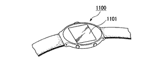
図9は、腕時計型電子機器の一例を示した斜視図である。図9において、符号1100は時計本体を示し、符号1101は上記実施形態の液晶表示装置を用いた液晶表示部を示している。
【0053】
図10は、ワープロ、パソコンなどの携帯型情報処理装置の一例を示した斜視図である。図10において、符号1200は情報処理装置、符号1202はキーボードなどの入力部、符号1204は情報処理装置本体、符号1206は上記実施形態の液晶表示装置を用いた液晶表示部を示している。
【0054】
図8〜図10に示す電子機器は、上記実施形態の液晶表示装置を用いた液晶表示部を備えているので、反射モード、透過モードにかかわらず明るく視認性に優れた表示が得られ、特に透過表示において高コントラストな表示部を有する電子機器を実現することができる。
【0055】
なお、本発明の技術範囲は上記実施の形態に限定されるものではなく、本発明の趣旨を逸脱しない範囲において種々の変更を加えることが可能である。例えば本発明は、上記実施の形態のようにアクティブマトリクス方式の半透過反射型カラー液晶表示装置に限ることなく、パッシブマトリクス方式、ドットマトリクス方式や白黒表示の液晶表示装置に適用することも可能である。
また、位相補償層60は必ずしも下偏光板28と下基板13との間の位置に設けられる必要はなく、透過表示領域にあればよい。
【0056】
【実施例】
本発明者らは、本発明の効果を実証するために本発明に係る構成の液晶表示装置を実際に作製し、透過率と反射率、およびコントラストを測定した。その結果について以下、報告する。
【0057】
本実施例では、色素濃度c(wt%)を変えた二種類の液晶セルC1,C2を作製した。
この液晶セルC1,C2を作製するに当たっては、誘電異方性が正の液晶組成物として、MJ96411(商品名、メルク社製)にカイラル物質を少量添加したものを用いた。この液晶組成物の屈折率異方性Δnは589nmの波長の光に対して0.12である。
また、二色性色素として下記の表1に示す4種類の色素(三菱化学社製)を用い、表1に示した混合比で混合して黒色色素とした。そして、この黒色色素を所定の濃度c(wt%)で上記液晶に混合してゲストホスト液晶とした。
【0058】
【表1】

そして、通常の方法により90°ツイストのTNセルを作製して上記ゲストホスト液晶を注入した後、上基板及び下基板の外面側に日東電工社製の偏光板SEG1425DU(商品名、偏光度:99.9%)を貼り付けた。この際、上下の偏光板の透過軸は、それぞれ上基板の配向膜のラビング方向,下基板の配向膜のラビング方向に平行となるようにしている。
【0060】
なお、セルギャップは、式(3)により、液晶層のリタデーションΔndがG(緑)の光に対して最適となる大きさとし、液晶セルC1,C2のセル厚(液晶層厚)をそれぞれ4.04μm,4.16μmとなるように構成した(表2参照)。すなわち、液晶セルC1,C2のリタデーションΔndはそれぞれ485nm,499nmとなり、550nm付近の波長の光に対して透過表示時のコントラストが最大となるようになっている。
【0061】
また、各液晶セルC1,C2について、上記液晶に混合するトータルの色素濃度cをそれぞれ3.6wt%,3.3wt%とし、光の吸収量(簡単のため、色素濃度c×液晶層厚みdとして計算している)が各液晶セルC1,C2についてそれぞれ14.5,13.7となるようにしている。
【0062】
【表2】
さらに、図7に示すように、下基板13と下偏光板28との間に配置する位相補償層60として、ポリカーボネイト製の二枚の位相差フィルム(第1位相差板61,第2位相差板62)を使用した。これらの第1位相差板61,第2位相差板62には、590nmの波長の光に対する位相差がそれぞれ460nm,220nmのものを用いている。
【0064】
また、図7に示すように、第1位相差板61,第2位相差板62の遅相軸を、下偏光板28の透過軸に対してそれぞれθ1,θ2だけ傾けて配置している。この角度θ1,θ2は、液晶セルC1についてはそれぞれ32°,33°、液晶セルC2についてはそれぞれ27°,38°とし、液晶の旋光による波長分散をより良く補償するとともに下偏光板28から入射した直線偏光の偏光面を90°だけ回転させるようにしている。なお、二色性色素の吸収によって偏光状態が変化するため、色素濃度の異なる液晶セルC1と液晶セルC2とでは、光学特性が最適となるθ1,θ2の条件が若干異なっている。
【0065】
また、式(1)においてNを1とした効果を調べるために、液晶層のリタデーションΔndが式(1)でNを2とした式に基づいて設定される二種類の比較用のセル(比較セルD1,比較セルD2)を作製した。比較セルD1,D2の液晶層はそれぞれ10.8μm,11.2μmとされ、いずれもG(緑)の光に対して最適な透過率が得られるようになっている。また、比較セルD1の液晶は二色性色素を混合しない通常のTNセルとし、比較セルD2では色素濃度cを1.3wt%として光の吸収量が液晶セルC1と略同一となるように構成している。
【0066】
さらに、位相補償層60の有無による透過表示時のコントラストの変化について調べるために、位相補償層60を設けない比較用のセル(第3比較セルD3,第4比較セルD4)を作製した。すなわち、比較セルD3,D4は、それぞれ液晶セルC1,C2の構成において、第1位相差板及び第2位相差板を省いた構成となっている。なお、下基板13に入射する光の偏光方向が上記液晶セルC1,C2と同一となるように、これらの比較セルD3,D4では、下偏光板28の透過軸を下基板13の配向膜のラビング方向に対して直交するように配置している。
【0067】
なお、上記の各セルC1,C2,D1〜D4において、反射特性と透過特性とを独立に調べるために、全面反射層を有するセルと反射層が全くないセルとの二種類を作製した。
そして、輝度計を用いてこれらのセルの反射特性及び透過特性を評価した。なお、輝度計はセル正面に配置され、セルの表示面から垂直に出射された光の輝度を測定するようになっている。そして、測定値に基づいて反射率及び透過率を算出している。
【0068】
〔階調反転に関する特性評価〕
まず、階調反転に対する効果を調べるために、反射層を有するセルを用いて0〜5Vまで電圧を印加しながら反射率を測定した。その結果、図11に示すように、比較セルD1では、印加電圧が0V〜1.3Vの範囲では反射率に変化はなく、1.3V付近で一旦増大した後、1.5V付近で反射率は減少し始めた。そして、印加電圧が2.1V付近で反射率は増大に転じ、印加電圧が3.4V以降で反射率は略一定の値となった。
【0069】
本来、二色性色素を含まない比較セルD1の構成では、印加電圧の有無に関わらず常に明表示を示すはずであり、ここでの反射率の変化は、純粋にリタデーションΔndと旋光性との関係として説明される。つまり、1.5V〜2.1V印加時の反射率の落ち込みは、電圧印加に伴う旋光性の低下によって反射光が一部上偏光板に吸収されたことに起因していると考えられる。なお、印加電圧1.3V〜1.5Vでの反射率の増大は実効的なΔndが式(2)を満たすような旋光性の高い状態になっていることに起因すると思われる。
【0070】
比較セルD2では、比較セルD1が示す反射率のカーブと比較して、1.8V〜3V印加時に反射率に落ち込みが見られる。落ち込みが見られた印加電圧の領域は上記比較セルD1において反射率の低下が見られたのと略同じ電圧領域であり、ここでの反射率の落ち込みも旋光性の消失の過程で生じる階調反転現象として説明できる。
これに対して、液晶セルC1では、電圧の増加に伴って反射率は増大し続け、階調反転のない良好な反射特性が得られた。また、5V印加時の反射率は25%程度となり、色素を混合した分反射率は低下しているものの、許容される範囲と考えられる。
【0071】
〔透過率及びコントラストに関する特性評価〕
次に、透過表示における透過率及びコントラストの評価を行なうために、反射層のないセルを用いて、0〜5Vまで電圧を印加しながら透過率を測定した。その結果、図12に示すように、比較セルD2,D3に関しては、4V印加時(明表示)に28%程度の透過率を示すものの、0V(暗表示)の透過率は0.5%程度あり、コントラストは55程度となった(表3参照)。
【0072】
【表3】
これに対して、液晶セルC1では4V印加時(明表示)の透過率と0V(暗表示)の透過率とはそれぞれ25.1%,0.065%となり、比較セルD2に比べて暗表示の輝度(光り抜け)が一桁程度改善された。これにより、コントラストは386に向上し、透過表示として十分な表示特性が得られた。また、液晶セルC1では位相補償層を設けたことと色素を混合したこととにより明表示における透過率は若干低下しているが、それほど大幅な低下ではなく、許容できる範囲である。また、図16に示したような円偏光を利用する従来の半透過反射型液晶表示装置の場合には、反射部をなくして画素全体を透過部にしたとしても、最大25%の透過率しか得られないことと比較すると、リサイクル光の利用により明るい表示が得られたと考えられる。
【0074】
色素濃度を薄くしたセルC2,D4についても上記と同様の測定を行なった。その結果、図13に示すように、4V印加時(明表示)の透過率はセルC2,D4についてそれぞれ26.73%,28.17%となり、色素濃度の濃い上記セルC1,D3に比べていずれも1.5%程度の改善が見られた(表3参照)。なお、セルC2については0V(暗表示)の透過率が0.088%と若干高くなったため、コントラストは304に低下したが、十分許容できる範囲と考えられる。
【0075】
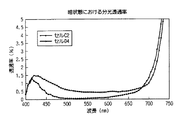
また、上述の暗表示における光抜けの改善効果を詳しく調べるために、分光透過率測定を行った。その結果、図14に示すように、液晶セルC1では可視光(400nm〜700nm)の広い波長範囲で波長分散の補償された均一な透過率が得られることがわかる。これにより、液晶セルC1では透過特性が可視光の略全範囲で最適化され、比較セルD3に比べて光抜けが大幅に低減された極めて良好な暗状態が得られることがわかる。
【0076】
セルC2,D4についても同様の測定を行った結果、図15に示すように、いずれのセルC2,D4についても色素濃度の濃い上記セルC1,D3に比べて若干透過率が増大している。これは、上記セルC1,D3では位相補償層によっても補償しきれずに液晶層に楕円偏光として入射した光は二色性色素によってある程度吸収されていたのに対して、色素濃度の薄いセルC2,D4ではこのような効果が弱まったためと考えられる。
【0077】
【発明の効果】
以上、詳細に説明したように、本発明の構成によれば、反射表示では液晶による光の旋光性と二色性色素による光の吸収を、透過表示では液晶による旋光性のみを利用することによって、反射表示及び透過表示の表示特性を共に向上させることができる。
また、透過表示部と反射表示部との同時刻における液晶の配向状態は基本的に同じでよく、複雑な構成を必要としないため、製造を容易にすることができる。
さらに、透過表示領域に液晶層の旋光による波長分散を補償する位相補償層が設けられているため、透過表示において高いコントラストを得ることができる。
【図面の簡単な説明】
【図1】 本発明の一実施形態の液晶表示装置の概略構成を示す断面図である。
【図2】 同、液晶表示装置の表示原理を説明するための図であって、表示原理の説明に必要な構成要素のみを示す図である。
【図3】 同、液晶表示装置の表示原理を説明するための図であって、表示原理の説明に必要な構成要素のみを示す図である。
【図4】 同、液晶表示装置の表示原理を説明するための図であって、表示原理の説明に必要な構成要素のみを示す図である。
【図5】 同、液晶表示装置の表示原理を説明するための図であって、表示原理の説明に必要な構成要素のみを示す図である。
【図6】 同、液晶表示装置の表示原理を説明するための図であって、表示原理の説明に必要な構成要素のみを示す図である。
【図7】 本発明の実施例の液晶表示装置の概略斜視図であり、構成部材の光学軸の配置を示す図である。
【図8】 本発明に係る電子機器の一例を示す斜視図である。
【図9】 本発明に係る電子機器の他の例を示す斜視図である。
【図10】 本発明に係る電子機器のさらに他の例を示す斜視図である。
【図11】 本発明の実施例の液晶表示装置における反射率を示す図である。
【図12】 本発明の実施例の液晶表示装置における透過率を示す図である。
【図13】 本発明の実施例の液晶表示装置における透過率を示す図である。
【図14】 本発明の実施例の液晶表示装置における暗表示の分光透過率を示す図である。
【図15】 本発明の実施例の液晶表示装置における暗表示の分光透過率を示す図である。
【図16】 従来の液晶表示装置の一例の概略構成を示す断面図である。
【図17】 同、液晶表示装置の表示原理を説明するための図であって、表示原理の説明に必要な構成要素のみを示す図である。
【符号の説明】
10 液晶表示装置
11 液晶セル
12 バックライト
13 下基板
14 上基板
16 液晶層
18 半透過反射層
18a 開口部
24,33 配向膜
28 下偏光板
36 上偏光板
50 カラーフィルタ
60 位相補償層
R 反射表示領域
T 透過表示領域
S 二色性色素分子
L 液晶分子[0001]
BACKGROUND OF THE INVENTION
The present invention relates to a liquid crystal display device and an electronic apparatus, and more particularly to a transflective liquid crystal display device that can display a sufficiently bright display not only in a reflection mode but also in a transmission mode. It is.
[0002]
[Prior art]
Conventionally, a liquid crystal display device has been proposed in which external light is used in a bright place in the same manner as a normal reflective liquid crystal display device, and in a dark place, the display can be visually recognized by an internal light source. This liquid crystal display device adopts a display method that has both a reflection mode and a transmission mode, and by switching to one of the display methods according to the surrounding brightness, even when the surroundings are dark while reducing power consumption Clear display can be performed. Hereinafter, in this specification, this type of liquid crystal display device is referred to as a “transflective liquid crystal display device”. As one form of the transflective liquid crystal display device, a reflective film in which an opening for light transmission is formed in a metal film such as aluminum is provided on the inner surface of the lower substrate, and this reflective film functions as a transflective film. Proposed. In the present specification, the liquid crystal side surface of each substrate constituting the liquid crystal display device is referred to as an “inner surface”, and the opposite surface is referred to as an “outer surface”.
[0003]
FIG. 16 shows an example of a transflective liquid crystal display device using this type of transflective film.
In this liquid
[0004]
Further, on the outer surface side of the
[0005]
The display principle of the transflective liquid
First, when performing dark display, a voltage is applied to the liquid crystal layer 103 (turned on) so that there is no phase difference in the
[0006]
On the other hand, in transmissive display, the light emitted from the
[0007]
Next, in the case of performing bright display, the voltage is not applied to the liquid crystal layer 103 (off state), and the phase difference due to the birefringence effect in the
[0008]
On the other hand, in the transmissive display, the clockwise circularly polarized light incident from the
[0009]
[Problems to be solved by the invention]
As described above, according to the liquid
One of the causes is that, as described in the explanation of the display principle with reference to FIG. 17, in the case of performing bright display by transmissive display, it is transmitted through the
[0010]
Another cause is that light emitted from the
[0011]
By the way, a liquid crystal to which a dichroic dye is added, that is, a so-called guest-host liquid crystal is well known. When this guest-host liquid crystal is used in a transflective liquid crystal display device, light passes through the liquid crystal layer twice in the reflective display portion, whereas light passes through the liquid crystal layer in the transmissive display portion. Since it is only once, the amount of light absorbed by the dichroic dye differs between the reflective display portion and the transmissive display portion. Therefore, when the dye density is adjusted so that a sufficient contrast can be obtained in the transmissive display, only a reflective display with a very low reflectance can be obtained. On the contrary, when the dye density is adjusted so that sufficient brightness and appropriate contrast can be obtained in the reflective display, there is a problem that the contrast becomes very low in the transmissive display.
[0012]
As described above, when the guest-host liquid crystal is applied to a transflective liquid crystal display device, it is difficult to obtain good optical characteristics in both reflective display and transmissive display. A method for solving this problem is disclosed in Japanese Patent Application Laid-Open No. 11-242226. However, in this method, it is essential that the liquid crystal alignment state at the same time be different between the reflective display portion and the transmissive display portion. For this reason, there is a drawback that the apparatus configuration is complicated and manufacturing is difficult.
[0013]
The present invention has been made in order to solve the above problems, and in a transflective liquid crystal display device capable of both reflective display and transmissive display, improves display characteristics in both display modes, An object of the present invention is to provide a liquid crystal display device capable of obtaining high contrast in transmissive display. It is another object of the present invention to provide an electronic apparatus including a liquid crystal display unit that improves display characteristics in both display modes of reflection display and transmission display and increases contrast in transmission display.
[0014]
[Means for Solving the Problems]
In order to achieve the above object, a liquid crystal display device of the present invention has a liquid crystal layer sandwiched between a pair of substrates facing each other, and has a transmissive display region and a reflective display region in one dot region. In the reflective liquid crystal display device, a first polarizing plate is provided on the outer surface side of one of the pair of substrates and a second polarizing plate is provided on the outer surface side of the other substrate of the pair of substrates, Between the second polarizing plate and the other substrate, the wavelength dispersion due to the optical rotation of the liquid crystal layer is compensated or relaxed, and the polarization direction of the linearly polarized light incident from the second polarizing plate is changed to that of the other substrate. A phase compensation layer that converts in a direction substantially perpendicular to the alignment direction of liquid crystal molecules adjacent to the inner surface is provided, and the liquid crystal layer includes a liquid crystal composition having a positive dielectric anisotropy mixed with a dichroic dye, The liquid crystal molecules of the liquid crystal layer are the pair of substrates. The substrate is twisted approximately 90 ° in a plane parallel to the substrate surface, and the transmission axis direction of the first polarizing plate and the alignment direction of the liquid crystal molecules adjacent to the inner surface of the one substrate are approximately parallel. And
[0015]
The operation at the time of dark display in the transmission mode of this configuration will be described with reference to FIG. FIG. 2 is a diagram for explaining the principle of the present invention, in which a
Here, the liquid crystal molecules L of the
[0016]
According to this configuration, in the transmissive display, the light that has been transmitted through the lower
In addition, since the phase of the light is shifted in advance in a direction to compensate or relax the wavelength dispersion due to the optical rotation of the
[0017]
Ideally, the wavelength dispersion due to the optical rotation of the liquid crystal is completely compensated over a wide wavelength range of visible light, so that the upper polarizing plate is reached as shown in the right part of FIG. All of the R, G, and B light is linearly polarized light containing no elliptically polarized light component, and the amount of emitted light can be made zero. Thereby, light omission in dark display can be effectively suppressed, and contrast in transmissive display can be improved.
[0018]
Although not shown, in this configuration, the reflection display uses the optical rotation by the liquid crystal and the light absorption by the dichroic dye S, so that the light of such a dye can be adjusted by adjusting the dye concentration. It is possible to simultaneously improve the display characteristics of both reflective display that performs display using absorption and transmissive display that uses only the optical rotation of light. Further, since circularly polarized light is not used for transmissive display, there is no component absorbed by the upper polarizing plate during bright display, and the transmissive display can be brightened. Furthermore, in the liquid crystal display device of the present invention, the alignment state of the liquid crystal at the same time in the transmissive display unit and the reflective display unit may be basically the same, and a complicated configuration is not required.
[0019]
The liquid crystal display device of the present invention is a transflective liquid crystal display device in which a liquid crystal layer is sandwiched between a pair of substrates facing each other, and a transmissive display region and a reflective display region are included in one dot region. A first polarizing plate is provided on the outer surface side of one substrate of the pair of substrates and a second polarizing plate is provided on the outer surface side of the other substrate of the pair of substrates, Between the second polarizing plate and the other substrate, Compensating or mitigating chromatic dispersion due to optical rotation of the liquid crystal layer , For linearly polarized light (wavelength λ) incident from the second polarizing plate Forms a phase difference of approximately λ And maintains the polarization state of the linearly polarized light The liquid crystal layer includes a liquid crystal composition having a positive dielectric anisotropy mixed with a dichroic dye, and the liquid crystal molecules of the liquid crystal layer are disposed between the pair of substrates. The second polarizing plate is twisted by approximately 90 ° in a plane parallel to the surface, and the transmission axis direction of the first polarizing plate is substantially parallel to the alignment direction of liquid crystal molecules adjacent to the inner surface of the first substrate. And the alignment direction of the liquid crystal molecules adjacent to the inner surface of the other substrate is substantially perpendicular.
[0020]
That is, in this configuration, the transmission axis of the lower polarizing plate is substantially perpendicular to the alignment direction of the liquid crystal molecules in contact with the inner surface of the lower substrate, and the phase difference formed by the phase compensation layer is approximately λ and is incident from the lower polarizing plate. The polarization state of linearly polarized light is maintained. Even with this configuration, the light incident on the liquid crystal layer from the lower polarizing plate has a polarization direction that is substantially perpendicular to the alignment direction of the liquid crystal molecules in contact with the inner surface of the lower substrate, and the phase is wavelength dispersion due to the optical rotation of the liquid crystal. It is possible to make a state shifted in a direction in which is compensated or relaxed. Therefore, the same operational effects as described above can be obtained, and the contrast of transmissive display can be improved.
[0021]
Furthermore, the liquid crystal display device of the present invention is a transflective liquid crystal display device in which a liquid crystal layer is sandwiched between a pair of substrates facing each other, and a transmissive display region and a reflective display region are included in one dot region. A first polarizing plate is provided on the outer surface side of one substrate of the pair of substrates and a second polarizing plate is provided on the outer surface side of the other substrate of the pair of substrates, Between the second polarizing plate and the other substrate, Compensating or mitigating chromatic dispersion due to optical rotation of the liquid crystal layer , For linearly polarized light (wavelength λ) incident from the second polarizing plate A phase compensation layer that forms a phase difference of approximately λ / 2 is provided, and the liquid crystal layer includes a liquid crystal composition having a positive dielectric anisotropy mixed with a dichroic dye, and the liquid crystal molecules of the liquid crystal layer include The pair of substrates is twisted approximately 90 ° in a plane parallel to the substrate surface, and the transmission axis direction of the first polarizing plate and the alignment direction of the liquid crystal molecules adjacent to the inner surface of the one substrate are approximately The angle formed between the slow axis of the phase compensation layer and the alignment direction of the liquid crystal molecules adjacent to the inner surface of the other substrate is θ, and the transmission axis of the second polarizing plate and the other substrate The angle between the alignment direction of the liquid crystal molecules in contact with the inner surface is approximately 2θ.
[0022]
According to this configuration, in the transmissive display, the light that has been transmitted through the lower polarizing plate and becomes linearly polarized light is rotated by the phase compensation layer by 2θ. The direction is substantially perpendicular to the alignment direction of the liquid crystal molecules in contact with the inner surface of the lower substrate. Therefore, this configuration can achieve the same effects as described above, and improve the contrast of transmissive display.
[0023]
The value of θ is preferably about 45 °. According to this configuration, in transmissive display, light that has been transmitted through the lower polarizing plate and converted into linearly polarized light becomes linearly polarized light with the polarization plane rotated by approximately 90 ° when transmitted through the phase compensation layer. Of the linearly polarized light, the light reflected by the back surface of the transflective layer is transmitted through the phase compensation layer, rotated again by 90 ° on the polarization plane, and returned to the lower polarizing plate. At this time, since the polarization direction of the linearly polarized light and the transmission axis of the lower polarizing plate are parallel, the linearly polarized light passes through the lower polarizing plate as it is. For this reason, the light reflected by the transflective layer can be reused to contribute to transmissive display, and a bright display is possible.
[0024]
Moreover, it is preferable to arrange | position a phase compensation layer in an outer surface side rather than a semi-transmissive reflective layer. According to this configuration, a bright display can be obtained without reducing the luminance in the reflective display. Of course, the phase compensation layer may be provided only in the transmissive display region. This configuration does not reduce the brightness of the reflective display.
The retardation value Δnd (Δn: refractive index anisotropy, d: liquid crystal layer thickness) of the liquid crystal layer may satisfy Δnd = 0.866 · λ (λ: 380 nm to 780 nm). According to this configuration, high display quality without gradation inversion can be obtained in reflective display. The basis for Δnd = 0.866 · λ will be described later in the section of [Embodiment of the Invention].
[0025]
The phase compensation layer may be configured as a combination of a plurality of retardation plates. According to this structure, the freedom degree of the member selection at the time of matching retardation of a phase compensation layer with respect to a liquid crystal layer increases.
A color filter may be provided between the upper substrate and the lower substrate. According to this configuration, it is possible to realize a liquid crystal display device capable of clear color display in both reflective display and transmissive display.
An electronic apparatus according to the present invention includes the liquid crystal display device according to the present invention.
According to this configuration, it is possible to provide an electronic apparatus including a liquid crystal display unit that is bright in both reflective display and transmissive display and particularly has high contrast in transmissive display.
[0026]
DETAILED DESCRIPTION OF THE INVENTION
Hereinafter, an embodiment of the present invention will be described. FIG. 1 is a cross-sectional view showing a schematic configuration of a liquid crystal display device of the present embodiment, and FIGS. 3 to 6 are diagrams for explaining the display principle. FIG. 8 is a diagram illustrating only components necessary for explaining the display principle, and FIGS. 8 to 10 are diagrams illustrating examples of electronic apparatuses including the liquid crystal display device. This embodiment is an example of an active matrix type transflective color liquid crystal display device. In all the following drawings, the film thicknesses and dimensional ratios of each component are appropriately changed in order to make the drawings easy to see. It is.
[0027]
As shown in FIG. 1, the liquid
[0028]
A
[0029]
A
[0030]
For the
[0031]
When this elliptically polarized light is transmitted through the twist-aligned
It is desirable that such chromatic dispersion compensation or relaxation be performed in a wide wavelength region of visible light, but it is not necessarily performed in the entire visible light range, and relaxation is performed in a part of the visible light wavelength region. Even just being done is effective.
[0032]
In addition, the
[0033]
The
The
On the other hand, a
[0034]
Both the
The transmission axis direction of the upper
[0035]
Further, the retardation Δnd of the liquid crystal layer 16 (Δn: refractive index anisotropy of the
Δnd = λ / 2 · (4N 2 -1) 0.5 ... (1)
[0036]
Expression (1) is generally known as a technique for minimizing the amount of transmitted light when the voltage is turned off in transmissive display, whereby high contrast can be obtained. In addition, when Δnd is large, when the voltage is gradually applied to the liquid crystal layer from the state where no voltage is applied, a phenomenon in which the display once becomes bright and then becomes dark again (gradation inversion phenomenon) is observed. Therefore, in the liquid crystal display device of this embodiment, the value of N is set to 1 so that the retardation Δnd of the
Δnd = 0.866λ (2)
[0037]
In other words, in order for TN liquid crystal to fully exhibit optical rotation, Δnd needs to satisfy the following Morgan condition (3), but in the process where effective Δnd decreases with voltage application, Since the propagating light is not sufficiently rotated and becomes elliptically polarized light, the light deviated from the polarization axis of the polarizing plate is partially absorbed by the polarizing plate and becomes dark.
Δnd> 2λ (3)
Such a gradation reversal phenomenon occurs even when the display is viewed from the front, and particularly appears at the time of reflective display in which light passes through the liquid crystal layer twice, which causes a reduction in visibility. In particular, when the effective Δnd at the same voltage is large, the degree of elliptically polarized light increases, and the drop in brightness at the time of gradation inversion increases. By minimizing the value of N, the amount of decrease in luminance due to such gradation inversion is minimized. In addition, since the liquid crystal layer thickness d is reduced, effects such as high luminance, high speed response, and low threshold voltage, which are found in a normal TN liquid crystal, can be obtained.
[0038]
The value of Δnd has a certain width with λ being a visible light wavelength range of 380 nm to 780 nm, and is set to an optimum value based on required specifications such as contrast. For example, high contrast can be obtained by matching λ in the above formula (2) with a wavelength of light close to G (green) having high visibility.
The
[0039]
Hereinafter, the display principle of the liquid
First, when performing dark display in the reflection mode (see FIG. 3), the
[0040]
The linearly polarized light rotates while being absorbed by the dichroic dye molecule S along the twist of the liquid crystal molecule L, reaches the
[0041]
Next, when bright display is performed in the reflection mode (see FIG. 4), a voltage is applied to the liquid crystal layer 16 (selection voltage application state), and the liquid crystal molecules L and the dichroic dye molecules S are placed on the substrate surface. It is assumed that it stands up in a substantially normal direction. In this case, the linearly polarized light parallel to the paper surface incident from above the upper
[0042]
On the other hand, when dark display is performed in the transmission mode (see FIG. 5), the alignment of the liquid crystal molecules L and the dichroic dye molecules S is set in the same manner as in the dark display in the reflection mode. The light incident from the
[0043]
When these R, G, and B light enters the
[0044]
Next, when the bright display is performed in the transmission mode (see FIG. 6), the orientation of the liquid crystal molecules L and the dichroic dye molecules S is substantially perpendicular to the substrate surface as in the case of the bright display in the reflection mode. The state of orientation is set. The light incident from the
[0045]
The R, G, and B light passes through the
Of the linearly polarized light that passes through the lower
[0046]
In the liquid
[0047]
The addition amount of the dichroic dye S is preferably smaller than that in the normal guest-host mode from the viewpoint of improving the brightness in the reflective display, and the brightness of the bright display from the viewpoint of improving the contrast in the transmissive display. It is preferable that the amount is as long as the thickness is not impaired. The reason for this is that, in the case of the present embodiment, in the reflective display, not only the absorption by the dye is used, but also the optical rotation of the light of the liquid crystal is used together. This is because if there are many dyes, the amount of absorption in bright display increases even if the molecules are vertically aligned, and the brightness of bright display decreases in both reflective display and transmissive display.
[0048]
On the other hand, in transmissive display, when performing dark display, elliptically polarized light that is slightly deviated from linearly polarized light without being fully compensated for chromatic dispersion by the
[0049]
Further, in the liquid
Furthermore, in the liquid crystal display device of the present embodiment, the alignment state of the liquid crystal molecules at the same time in the transmissive display region T and the reflective display region R may be basically the same, and a complicated configuration is not required. Easy.
[0050]
In addition, since the liquid crystal layer thickness is set so that the retardation value Δnd of the
Further, in the transmissive display, the wavelength dispersion due to the rotation of the
[0051]
[Electronics]
An example of an electronic apparatus including the liquid crystal display device of the above embodiment will be described.
FIG. 8 is a perspective view showing an example of a mobile phone. In FIG. 8,
[0052]
FIG. 9 is a perspective view showing an example of a wristwatch type electronic apparatus. In FIG. 9,
[0053]
FIG. 10 is a perspective view showing an example of a portable information processing apparatus such as a word processor or a personal computer. In FIG. 10,
[0054]
Since the electronic apparatus shown in FIGS. 8 to 10 includes a liquid crystal display unit using the liquid crystal display device of the above embodiment, a bright and excellent display can be obtained regardless of the reflection mode and the transmission mode. An electronic device having a display portion with high contrast in transmissive display can be realized.
[0055]
The technical scope of the present invention is not limited to the above embodiment, and various modifications can be made without departing from the spirit of the present invention. For example, the present invention is not limited to the active matrix transflective color liquid crystal display device as in the above embodiment, but can also be applied to a passive matrix method, a dot matrix method, and a monochrome display liquid crystal display device. is there.
Further, the
[0056]
【Example】
In order to demonstrate the effect of the present invention, the inventors actually manufactured a liquid crystal display device having a configuration according to the present invention, and measured transmittance, reflectance, and contrast. The results are reported below.
[0057]
In this example, two types of liquid crystal cells C1 and C2 with different dye concentrations c (wt%) were produced.
In manufacturing the liquid crystal cells C1 and C2, a liquid crystal composition having a positive dielectric anisotropy having a small amount of a chiral substance added to MJ96411 (trade name, manufactured by Merck & Co., Inc.) was used. The refractive index anisotropy Δn of this liquid crystal composition is 0.12 with respect to light having a wavelength of 589 nm.
Further, as the dichroic dye, four kinds of dyes (manufactured by Mitsubishi Chemical Corporation) shown in Table 1 below were used and mixed at the mixing ratio shown in Table 1 to obtain a black dye. And this black pigment | dye was mixed with the said liquid crystal by predetermined | prescribed density | concentration c (wt%), and it was set as the guest host liquid crystal.
[0058]
[Table 1]
Then, a 90 ° twisted TN cell was prepared by a normal method and the guest host liquid crystal was injected. Then, a polarizing plate SEG1425DU (trade name, polarization degree: 99 manufactured by Nitto Denko Corporation) was formed on the outer surface side of the upper substrate and the lower substrate. 9%). At this time, the transmission axes of the upper and lower polarizing plates are parallel to the rubbing direction of the alignment film on the upper substrate and the rubbing direction of the alignment film on the lower substrate, respectively.
[0060]
It should be noted that the cell gap is set to a size at which the retardation Δnd of the liquid crystal layer is optimal for G (green) light according to the equation (3), and the cell thickness (liquid crystal layer thickness) of the liquid crystal cells C1 and C2 is 4. It comprised so that it might become 04 micrometers and 4.16 micrometers (refer Table 2). That is, the retardations Δnd of the liquid crystal cells C1 and C2 are 485 nm and 499 nm, respectively, so that the contrast at the time of transmissive display is maximized with respect to light having a wavelength near 550 nm.
[0061]
Further, for each of the liquid crystal cells C1 and C2, the total dye concentration c mixed with the liquid crystal is 3.6 wt% and 3.3 wt%, respectively, and the amount of light absorption (dye concentration c × liquid crystal layer thickness d for simplicity). However, the liquid crystal cells C1 and C2 are 14.5 and 13.7, respectively.
[0062]
[Table 2]
Further, as shown in FIG. 7, two retardation films (a
[0064]
Further, as shown in FIG. 7, the slow axes of the
[0065]
Further, in order to investigate the effect of setting N to 1 in the formula (1), two types of comparison cells (comparison) in which the retardation Δnd of the liquid crystal layer is set based on the formula in which N is set to 2 in the formula (1) Cell D1 and comparative cell D2) were prepared. The liquid crystal layers of the comparison cells D1 and D2 are 10.8 μm and 11.2 μm, respectively, so that the optimum transmittance can be obtained for G (green) light. Further, the liquid crystal of the comparative cell D1 is a normal TN cell in which no dichroic dye is mixed, and the comparative cell D2 is configured such that the dye concentration c is 1.3 wt% and the light absorption amount is substantially the same as that of the liquid crystal cell C1. is doing.
[0066]
Furthermore, in order to investigate the change in contrast during transmissive display depending on the presence or absence of the
[0067]
In each of the cells C1, C2, D1 to D4 described above, two types of cells, a cell having an entire reflective layer and a cell having no reflective layer, were prepared in order to independently examine the reflection characteristics and the transmission characteristics.
Then, the reflection characteristics and transmission characteristics of these cells were evaluated using a luminance meter. The luminance meter is arranged in front of the cell and measures the luminance of light emitted vertically from the display surface of the cell. Then, the reflectance and transmittance are calculated based on the measured values.
[0068]
[Characteristic evaluation regarding gradation inversion]
First, in order to investigate the effect on gradation inversion, the reflectance was measured while applying a voltage from 0 to 5 V using a cell having a reflective layer. As a result, as shown in FIG. 11, in the comparative cell D1, there is no change in the reflectance when the applied voltage is in the range of 0V to 1.3V, and after increasing once near 1.3V, the reflectance near 1.5V. Began to decline. The reflectance started to increase when the applied voltage was around 2.1 V, and the reflectance became a substantially constant value after the applied voltage was 3.4 V.
[0069]
Originally, in the configuration of the comparative cell D1 that does not include the dichroic dye, the bright display should always be displayed regardless of the presence or absence of the applied voltage, and the change in reflectance here is purely between the retardation Δnd and the optical rotation. Explained as a relationship. That is, it is considered that the drop in reflectance when 1.5 V to 2.1 V is applied is due to the fact that the reflected light is partially absorbed by the upper polarizing plate due to a decrease in optical rotation accompanying voltage application. The increase in reflectance at an applied voltage of 1.3 V to 1.5 V is considered to be due to the fact that the optical rotation is high so that the effective Δnd satisfies the formula (2).
[0070]
In the comparison cell D2, a drop in reflectance is observed when 1.8V to 3V is applied, as compared to the reflectance curve indicated by the comparison cell D1. The region of the applied voltage where the drop was observed is substantially the same voltage region as that in which the reflectance was lowered in the comparative cell D1, and the drop in the reflectance here is also a gradation generated in the process of loss of optical rotation. This can be explained as an inversion phenomenon.
On the other hand, in the liquid crystal cell C1, the reflectance continued to increase as the voltage increased, and good reflection characteristics without gradation inversion were obtained. Further, the reflectivity when 5 V is applied is about 25%, and although the reflectivity is decreased by mixing the dye, it is considered to be an allowable range.
[0071]
[Characteristic evaluation regarding transmittance and contrast]
Next, in order to evaluate the transmittance and contrast in the transmissive display, the transmittance was measured using a cell without a reflective layer while applying a voltage from 0 to 5V. As a result, as shown in FIG. 12, regarding the comparative cells D2 and D3, although the transmittance is about 28% when 4V is applied (bright display), the transmittance at 0V (dark display) is about 0.5%. Yes, the contrast was about 55 (see Table 3).
[0072]
[Table 3]
On the other hand, in the liquid crystal cell C1, the transmittance when 4V is applied (bright display) and the transmittance at 0V (dark display) are 25.1% and 0.065%, respectively, which is darker than that of the comparative cell D2. The brightness (light loss) has been improved by an order of magnitude. Thereby, the contrast was improved to 386, and display characteristics sufficient for transmissive display were obtained. Further, in the liquid crystal cell C1, the transmittance in the bright display is slightly lowered due to the provision of the phase compensation layer and the mixing of the pigment, but it is not so much reduced and is in an allowable range. Further, in the case of the conventional transflective liquid crystal display device using circularly polarized light as shown in FIG. 16, even if the reflective portion is eliminated and the entire pixel is made a transmissive portion, the transmittance is only 25% at maximum. It is considered that bright display was obtained by using recycled light as compared with the case where it was not obtained.
[0074]
Measurements similar to those described above were performed for the cells C2 and D4 having a reduced pigment concentration. As a result, as shown in FIG. 13, the transmittance when 4V is applied (bright display) is 26.73% and 28.17% for the cells C2 and D4, respectively, which is higher than that of the cells C1 and D3 having a high pigment concentration. In all cases, an improvement of about 1.5% was observed (see Table 3). Note that the transmittance of 0V (dark display) for cell C2 was slightly increased to 0.088%, and thus the contrast decreased to 304, but is considered to be a sufficiently acceptable range.
[0075]
Further, in order to examine in detail the effect of improving light leakage in the above-described dark display, spectral transmittance measurement was performed. As a result, as shown in FIG. 14, it can be seen that the liquid crystal cell C1 can obtain a uniform transmittance with compensated chromatic dispersion in a wide wavelength range of visible light (400 nm to 700 nm). Thus, it can be seen that the liquid crystal cell C1 has a transmission characteristic optimized in substantially the entire range of visible light, and a very good dark state in which light leakage is significantly reduced as compared with the comparative cell D3.
[0076]
As a result of performing the same measurement for the cells C2 and D4, as shown in FIG. 15, the transmittance of the cells C2 and D4 is slightly increased as compared with the cells C1 and D3 having a high pigment concentration. This is because in the cells C1 and D3, light incident as elliptically polarized light on the liquid crystal layer without being compensated by the phase compensation layer was absorbed to some extent by the dichroic dye, whereas the cells C2 and D2 having a low dye concentration were used. It is thought that this effect was weakened in D4.
[0077]
【The invention's effect】
As described above in detail, according to the configuration of the present invention, by utilizing the optical rotatory power of the liquid crystal and the absorption of the light by the dichroic dye in the reflective display, by using only the optical rotatory power of the liquid crystal in the transmissive display. Both the display characteristics of the reflective display and the transmissive display can be improved.
In addition, the alignment state of the liquid crystal in the transmissive display portion and the reflective display portion at the same time may be basically the same, and a complicated configuration is not required, so that manufacturing can be facilitated.
Furthermore, since a phase compensation layer that compensates for wavelength dispersion caused by optical rotation of the liquid crystal layer is provided in the transmissive display region, high contrast can be obtained in transmissive display.
[Brief description of the drawings]
FIG. 1 is a cross-sectional view showing a schematic configuration of a liquid crystal display device according to an embodiment of the present invention.
FIG. 2 is a diagram for explaining the display principle of the liquid crystal display device, and showing only the components necessary for explaining the display principle.
FIG. 3 is a diagram for explaining the display principle of the liquid crystal display device, and showing only the components necessary for explaining the display principle.
FIG. 4 is a diagram for explaining the display principle of the liquid crystal display device, and showing only the components necessary for explaining the display principle.
FIG. 5 is a diagram for explaining the display principle of the liquid crystal display device, and showing only the components necessary for explaining the display principle.
FIG. 6 is a diagram for explaining the display principle of the liquid crystal display device, and showing only the components necessary for explaining the display principle.
FIG. 7 is a schematic perspective view of a liquid crystal display device according to an embodiment of the present invention, and is a diagram illustrating an arrangement of optical axes of constituent members.
FIG. 8 is a perspective view showing an example of an electronic apparatus according to the invention.
FIG. 9 is a perspective view showing another example of an electronic apparatus according to the invention.
FIG. 10 is a perspective view showing still another example of the electronic apparatus according to the invention.
FIG. 11 is a diagram showing reflectance in a liquid crystal display device according to an embodiment of the present invention.
FIG. 12 is a diagram showing transmittance in a liquid crystal display device according to an embodiment of the present invention.
FIG. 13 is a diagram showing the transmittance in the liquid crystal display device according to the embodiment of the present invention.
FIG. 14 is a diagram showing spectral transmittance of dark display in the liquid crystal display device according to the embodiment of the present invention.
FIG. 15 is a diagram illustrating spectral transmittance of dark display in the liquid crystal display device according to the embodiment of the present invention.
FIG. 16 is a cross-sectional view showing a schematic configuration of an example of a conventional liquid crystal display device.
FIG. 17 is a diagram for explaining the display principle of the liquid crystal display device, and showing only the components necessary for explaining the display principle.
[Explanation of symbols]
10 Liquid crystal display device
11 Liquid crystal cell
12 Backlight
13 Lower substrate
14 Upper substrate
16 Liquid crystal layer
18 Transflective layer
18a opening
24, 33 Alignment film
28 Lower polarizing plate
36 Upper Polarizer
50 color filter
60 Phase compensation layer
R Reflective display area
T Transparent display area
S Dichroic dye molecule
L Liquid crystal molecules
Claims (10)
前記一対の基板の一方の基板の外面側に第1偏光板が設けられるとともに前記一対の基板の他方の基板の外面側に第2偏光板が設けられ、前記第2偏光板と前記他方の基板との間に、前記液晶層の旋光による波長分散を補償又は緩和するとともに、前記第2偏光板から入射された直線偏光の偏光方向を前記他方の基板の内面に近接する液晶分子の配向方向に概ね垂直な方向に変換する位相補償層が設けられ、
前記液晶層は、二色性色素が混入された誘電異方性が正の液晶組成物を含み、前記液晶層の液晶分子は、前記一対の基板の間において基板面に平行な面内で略90°ねじれており、前記第1偏光板の透過軸方向と前記一方の基板の内面に近接する液晶分子の配向方向とは概ね平行であることを特徴とする、液晶表示装置。A transflective liquid crystal display device having a liquid crystal layer sandwiched between a pair of substrates facing each other and having a transmissive display region and a reflective display region in one dot region,
A first polarizing plate is provided on an outer surface side of one substrate of the pair of substrates, and a second polarizing plate is provided on an outer surface side of the other substrate of the pair of substrates, and the second polarizing plate and the other substrate And compensating or mitigating chromatic dispersion caused by optical rotation of the liquid crystal layer, and aligning the polarization direction of the linearly polarized light incident from the second polarizing plate with the alignment direction of liquid crystal molecules adjacent to the inner surface of the other substrate. A phase compensation layer that converts in a substantially vertical direction is provided,
The liquid crystal layer includes a liquid crystal composition having a positive dielectric anisotropy mixed with a dichroic dye, and the liquid crystal molecules of the liquid crystal layer are substantially in a plane parallel to the substrate surface between the pair of substrates. A liquid crystal display device, wherein the liquid crystal display device is twisted by 90 °, and the alignment direction of liquid crystal molecules adjacent to the inner surface of the one substrate is substantially parallel to the first polarizing plate.
前記一対の基板の一方の基板の外面側に第1偏光板が設けられるとともに前記一対の基板の他方の基板の外面側に第2偏光板が設けられ、前記第2偏光板と前記他方の基板との間に、前記液晶層の旋光による波長分散を補償又は緩和するとともに、前記第2偏光板から入射された直線偏光(波長λ)に対して概ねλの位相差を形成し該直線偏光の偏光状態を保持する位相補償層が設けられ、
前記液晶層は、二色性色素が混入された誘電異方性が正の液晶組成物を含み、前記液晶層の液晶分子は、前記一対の基板の間において基板面に平行な面内で略90°ねじれており、前記第1偏光板の透過軸方向と前記第1基板の内面に近接する液晶分子の配向方向とは概ね平行であり、前記第2偏光板の透過軸方向と前記他方の基板の内面に近接する液晶分子の配向方向とは概ね垂直であることを特徴とする、液晶表示装置。A transflective liquid crystal display device having a liquid crystal layer sandwiched between a pair of substrates facing each other and having a transmissive display region and a reflective display region in one dot region,
A first polarizing plate is provided on an outer surface side of one substrate of the pair of substrates, and a second polarizing plate is provided on an outer surface side of the other substrate of the pair of substrates, and the second polarizing plate and the other substrate And compensates or relaxes the chromatic dispersion caused by the optical rotation of the liquid crystal layer, and forms a phase difference of approximately λ with respect to the linearly polarized light (wavelength λ) incident from the second polarizing plate . A phase compensation layer that maintains the polarization state is provided,
The liquid crystal layer includes a liquid crystal composition having a positive dielectric anisotropy mixed with a dichroic dye, and the liquid crystal molecules of the liquid crystal layer are substantially in a plane parallel to the substrate surface between the pair of substrates. 90 ° twisted, the transmission axis direction of the first polarizing plate and the alignment direction of the liquid crystal molecules adjacent to the inner surface of the first substrate are substantially parallel, and the transmission axis direction of the second polarizing plate and the other A liquid crystal display device characterized by being substantially perpendicular to an alignment direction of liquid crystal molecules adjacent to an inner surface of a substrate.
前記一対の基板の一方の基板の外面側に第1偏光板が設けられるとともに前記一対の基板の他方の基板の外面側に第2偏光板が設けられ、前記第2偏光板と前記他方の基板との間に、前記液晶層の旋光による波長分散を補償又は緩和するとともに、前記第2偏光板から入射された直線偏光(波長λ)に対して概ねλ/2の位相差を形成する位相補償層が設けられ、
前記液晶層は、二色性色素が混入された誘電異方性が正の液晶組成物を含み、前記液晶層の液晶分子は、前記一対の基板の間において基板面に平行な面内で略90°ねじれており、前記第1偏光板の透過軸方向と前記一方の基板の内面に近接する液晶分子の配向方向とは概ね平行であり、前記位相補償層の遅相軸と前記他方の基板の内面に近接する液晶分子の配向方向とのなす角度がθであり、前記第2偏光板の透過軸と前記他方の基板の内面に接する液晶分子の配向方向とのなす角度が概ね2θであることを特徴とする、液晶表示装置。A transflective liquid crystal display device having a liquid crystal layer sandwiched between a pair of substrates facing each other and having a transmissive display region and a reflective display region in one dot region,
A first polarizing plate is provided on an outer surface side of one substrate of the pair of substrates, and a second polarizing plate is provided on an outer surface side of the other substrate of the pair of substrates, and the second polarizing plate and the other substrate between, as well as compensation or relax the wavelength dispersion by the optical rotation of the liquid crystal layer, a phase compensation generally forms a phase difference of lambda / 2 with respect to linearly polarized light which is incident (wavelength lambda) from said second polarizer Layers are provided,
The liquid crystal layer includes a liquid crystal composition having a positive dielectric anisotropy mixed with a dichroic dye, and the liquid crystal molecules of the liquid crystal layer are substantially in a plane parallel to the substrate surface between the pair of substrates. 90 ° twisted, the transmission axis direction of the first polarizing plate and the alignment direction of the liquid crystal molecules close to the inner surface of the one substrate are substantially parallel, and the slow axis of the phase compensation layer and the other substrate The angle between the alignment direction of the liquid crystal molecules adjacent to the inner surface of the substrate is θ, and the angle between the transmission axis of the second polarizing plate and the alignment direction of the liquid crystal molecules in contact with the inner surface of the other substrate is approximately 2θ. A liquid crystal display device.
Priority Applications (1)
| Application Number | Priority Date | Filing Date | Title |
|---|---|---|---|
| JP2002174518A JP4129724B2 (en) | 2002-06-14 | 2002-06-14 | Liquid crystal display device and electronic apparatus using the same |
Applications Claiming Priority (1)
| Application Number | Priority Date | Filing Date | Title |
|---|---|---|---|
| JP2002174518A JP4129724B2 (en) | 2002-06-14 | 2002-06-14 | Liquid crystal display device and electronic apparatus using the same |
Publications (3)
| Publication Number | Publication Date |
|---|---|
| JP2004020832A JP2004020832A (en) | 2004-01-22 |
| JP2004020832A5 JP2004020832A5 (en) | 2005-10-13 |
| JP4129724B2 true JP4129724B2 (en) | 2008-08-06 |
Family
ID=31173467
Family Applications (1)
| Application Number | Title | Priority Date | Filing Date |
|---|---|---|---|
| JP2002174518A Expired - Fee Related JP4129724B2 (en) | 2002-06-14 | 2002-06-14 | Liquid crystal display device and electronic apparatus using the same |
Country Status (1)
| Country | Link |
|---|---|
| JP (1) | JP4129724B2 (en) |
Families Citing this family (2)
| Publication number | Priority date | Publication date | Assignee | Title |
|---|---|---|---|---|
| CN100437267C (en) * | 2004-05-28 | 2008-11-26 | 鸿富锦精密工业(深圳)有限公司 | Semi penetration semi reflective liquid crystal display device |
| CN111033368A (en) * | 2017-09-06 | 2020-04-17 | 索尼公司 | Optical device, display device, and electronic apparatus |
-
2002
- 2002-06-14 JP JP2002174518A patent/JP4129724B2/en not_active Expired - Fee Related
Also Published As
| Publication number | Publication date |
|---|---|
| JP2004020832A (en) | 2004-01-22 |
Similar Documents
| Publication | Publication Date | Title |
|---|---|---|
| JP3410666B2 (en) | Liquid crystal display | |
| US6341002B1 (en) | Liquid crystal display device | |
| US7248311B2 (en) | Liquid crystal display device and electronic apparatus | |
| JP3493321B2 (en) | Liquid crystal display | |
| JP2000131681A (en) | Semi-transmission type liquid crystal display device | |
| JP3827587B2 (en) | Reflective or transflective liquid crystal display device | |
| KR20070013889A (en) | Liquid crystal display device | |
| US8085370B2 (en) | Single-polarizer reflective bistable twisted nematic (BTN) liquid crystal display device | |
| JP2000029010A (en) | Liquid crystal display device | |
| JP3410665B2 (en) | Liquid crystal display | |
| JP3705184B2 (en) | Liquid crystal device and electronic device | |
| JP4129724B2 (en) | Liquid crystal display device and electronic apparatus using the same | |
| JP4337843B2 (en) | Liquid crystal display device and electronic device | |
| JP2000347187A (en) | Reflective liquid crystal display device | |
| JP4141746B2 (en) | Liquid crystal display device and electronic apparatus using the same | |
| JP2003140154A (en) | Liquid crystal display device | |
| JP3619506B2 (en) | Liquid crystal display | |
| JP3655911B2 (en) | Liquid crystal display | |
| JP2004219553A (en) | Liquid crystal display device and electronic appliance | |
| JP3655903B2 (en) | Liquid crystal display | |
| JP3619507B2 (en) | Liquid crystal display | |
| JP2004219552A (en) | Liquid crystal display device and electronic appliance | |
| JP4609382B2 (en) | Liquid crystal display device and electronic device | |
| JP3619518B2 (en) | Liquid crystal display | |
| JP2003330024A (en) | Liquid crystal display and electronic equipment |
Legal Events
| Date | Code | Title | Description |
|---|---|---|---|
| A521 | Written amendment |
Free format text: JAPANESE INTERMEDIATE CODE: A523 Effective date: 20050603 |
|
| A621 | Written request for application examination |
Free format text: JAPANESE INTERMEDIATE CODE: A621 Effective date: 20050603 |
|
| A521 | Written amendment |
Free format text: JAPANESE INTERMEDIATE CODE: A821 Effective date: 20050606 |
|
| A977 | Report on retrieval |
Free format text: JAPANESE INTERMEDIATE CODE: A971007 Effective date: 20080204 |
|
| A131 | Notification of reasons for refusal |
Free format text: JAPANESE INTERMEDIATE CODE: A131 Effective date: 20080219 |
|
| A521 | Written amendment |
Free format text: JAPANESE INTERMEDIATE CODE: A523 Effective date: 20080326 |
|
| TRDD | Decision of grant or rejection written | ||
| A01 | Written decision to grant a patent or to grant a registration (utility model) |
Free format text: JAPANESE INTERMEDIATE CODE: A01 Effective date: 20080425 |
|
| A01 | Written decision to grant a patent or to grant a registration (utility model) |
Free format text: JAPANESE INTERMEDIATE CODE: A01 |
|
| A61 | First payment of annual fees (during grant procedure) |
Free format text: JAPANESE INTERMEDIATE CODE: A61 Effective date: 20080508 |
|
| R150 | Certificate of patent or registration of utility model |
Free format text: JAPANESE INTERMEDIATE CODE: R150 |
|
| FPAY | Renewal fee payment (event date is renewal date of database) |
Free format text: PAYMENT UNTIL: 20110530 Year of fee payment: 3 |
|
| FPAY | Renewal fee payment (event date is renewal date of database) |
Free format text: PAYMENT UNTIL: 20120530 Year of fee payment: 4 |
|
| FPAY | Renewal fee payment (event date is renewal date of database) |
Free format text: PAYMENT UNTIL: 20120530 Year of fee payment: 4 |
|
| FPAY | Renewal fee payment (event date is renewal date of database) |
Free format text: PAYMENT UNTIL: 20130530 Year of fee payment: 5 |
|
| FPAY | Renewal fee payment (event date is renewal date of database) |
Free format text: PAYMENT UNTIL: 20140530 Year of fee payment: 6 |
|
| LAPS | Cancellation because of no payment of annual fees |