JP4122594B2 - Optical device, and projector device, rear projector device, and multi-projector device using the same - Google Patents
Optical device, and projector device, rear projector device, and multi-projector device using the same Download PDFInfo
- Publication number
- JP4122594B2 JP4122594B2 JP29941798A JP29941798A JP4122594B2 JP 4122594 B2 JP4122594 B2 JP 4122594B2 JP 29941798 A JP29941798 A JP 29941798A JP 29941798 A JP29941798 A JP 29941798A JP 4122594 B2 JP4122594 B2 JP 4122594B2
- Authority
- JP
- Japan
- Prior art keywords
- light source
- light
- lens
- projector
- image
- Prior art date
- Legal status (The legal status is an assumption and is not a legal conclusion. Google has not performed a legal analysis and makes no representation as to the accuracy of the status listed.)
- Expired - Fee Related
Links
Images


Classifications
-
- H—ELECTRICITY
- H04—ELECTRIC COMMUNICATION TECHNIQUE
- H04N—PICTORIAL COMMUNICATION, e.g. TELEVISION
- H04N9/00—Details of colour television systems
- H04N9/12—Picture reproducers
- H04N9/31—Projection devices for colour picture display, e.g. using electronic spatial light modulators [ESLM]
- H04N9/3102—Projection devices for colour picture display, e.g. using electronic spatial light modulators [ESLM] using two-dimensional electronic spatial light modulators
- H04N9/3111—Projection devices for colour picture display, e.g. using electronic spatial light modulators [ESLM] using two-dimensional electronic spatial light modulators for displaying the colours sequentially, e.g. by using sequentially activated light sources
- H04N9/3114—Projection devices for colour picture display, e.g. using electronic spatial light modulators [ESLM] using two-dimensional electronic spatial light modulators for displaying the colours sequentially, e.g. by using sequentially activated light sources by using a sequential colour filter producing one colour at a time
-
- G—PHYSICS
- G03—PHOTOGRAPHY; CINEMATOGRAPHY; ANALOGOUS TECHNIQUES USING WAVES OTHER THAN OPTICAL WAVES; ELECTROGRAPHY; HOLOGRAPHY
- G03B—APPARATUS OR ARRANGEMENTS FOR TAKING PHOTOGRAPHS OR FOR PROJECTING OR VIEWING THEM; APPARATUS OR ARRANGEMENTS EMPLOYING ANALOGOUS TECHNIQUES USING WAVES OTHER THAN OPTICAL WAVES; ACCESSORIES THEREFOR
- G03B21/00—Projectors or projection-type viewers; Accessories therefor
- G03B21/14—Details
- G03B21/28—Reflectors in projection beam
-
- H—ELECTRICITY
- H04—ELECTRIC COMMUNICATION TECHNIQUE
- H04N—PICTORIAL COMMUNICATION, e.g. TELEVISION
- H04N9/00—Details of colour television systems
- H04N9/12—Picture reproducers
- H04N9/31—Projection devices for colour picture display, e.g. using electronic spatial light modulators [ESLM]
- H04N9/3141—Constructional details thereof
- H04N9/315—Modulator illumination systems
- H04N9/3152—Modulator illumination systems for shaping the light beam
Description
【0001】
【発明の属する技術分野】
本発明は、光学装置、並びに、それを用いたプロジェクタ装置、リアプロジェクタ装置及びマルチプロジェクタ装置に関するものである。
【0002】
【従来の技術】
近年、大画面の画像表示装置としてプロジェクタ装置が注目されている。小型で高精細・高輝度のCRTを用いたCRTプロジェクタ装置、液晶パネルを用いた液晶プロジェクタ装置、DMD(Digital Micromirror Device)を用いたDMDプロジェクタ装置等が製品化されている。中でもDMDはディジタル駆動素子であるため原理的にコンピュータ情報の表示、ディジタルテレビ放送との相性が良く、現在もっとも期待されているプロジェクタ装置用ライトバルブの一つである。
【0003】
まず、DMDの構造を説明する。DMDは半導体の製造技術を用い、シリコン基板上に例えば16μm×16μmの微小なミラーを多数配列し、これらを電気的に制御することにより入射光の反射方向をミラー毎にコントロールするもので、各微小ミラーが画素に相当し、投写レンズを介してスクリーンに投写することによって映像情報を表示する。図18は、2ピクセルのDMD素子の構成を示す斜視図である。図において510、511はマイクロミラーで、素子600の法線からそれぞれ+10度あるいは−10度に傾いているところを示している。
【0004】
マイクロミラー510、511の表面にはアルミニウムが蒸着され、高い反射率を持つ例えば正方形のミラーとして作用する。このマイクロミラーを傾ける角度により光が反射する方向を切り替え、さらに切り替え時間の調整により階調表現が実現できる。このようなマイクロミラーが所定のフォーマットに従って、例えば480×640、600×800というように2次元配列されライトバルブとして構成される。DMDの詳細については、Larry J. Hornbeck, ”Digital Light Processing for High-Brightness, High-Resolution Applications.”, SPIE Vol.3013, pp.27-40,等に詳しく紹介されているので、ここではこれ以上の詳しい説明は省略する。
【0005】
次に、DMDをライトバルブとして用いたビデオプロジェクタの光学系の原理を図19で説明する。図19は単板式DMDプロジェクタ装置によるDMDの表示原理を説明する概念図であり、150はメタルハライドランプなどの光源、601はDMD、このうち512、513は+10度に回転したマイクロミラー、514は−10度に回転したマイクロミラーを拡大して概念的に示している。また、602は不要光を吸収する光アブソーバ、80は投写レンズである。図19において光源150から出射された光は、DMD601の法線方向から+20度傾いた方向からDMD素子に入射される。−10度に回転したマイクロミラー514の反射光は投写レンズから外れて光アブソーバ602に吸収され、図示しないスクリーン上では黒点の画素となる。一方、+10度に回転したマイクロミラー512、513の反射光は投写レンズで集光されてスクリーン上で明点の画素となり、DMD601上のマイクロミラー像がスクリーンに映像として拡大投写される。なお、回転カラーフィルタを光路中に配置した単板式プロジェクタ装置や、ダイクロイックプリズムやダイクロイックフィルタを配列して、RGB3原色に分解して各色毎に変調する3板式のプロジェクタ装置などにより、カラー画像の表示を行なうことも可能である。
【0006】
さて、以上に述べたDMDの動作原理から明らかなように、DMDを照明する際の最も特徴的な条件は、被照明面の法線方向から所定の角度をもって照明光を入射させなければならないということである。図20はDMDを用いてカラー画像を表示する従来のカラー画像表示装置を示す模式的構成図であり、例えば特開平10−039240号に開示されている。図20において、603はDMD、515、516はDMDを構成するマイクロミラー、151は平行白色光を出射する平行白色光源、400は入射角度に対応して特定波長の透過光を生じさせる光学薄膜、800は結像レンズ、900はスクリーンである。
【0007】
ここで最も注目すべきは、DMD603に対する平行白色光源151の配置であり、DMD603の2次元配列された各ミラーに平行白色光を入射させるべく、平行白色光源151はDMD603に対して所定の角度α1だけ傾いた方向に配置されている。DMD603に入射した白色光は、傾斜角度θ1が制御されたミラー515、516で反射され、結像レンズ800によってスクリーン900に導かれる。光学薄膜400はカラー画像を表示させるために挿入されているが、ここでは動作の説明は省略する。以上説明したような斜方照明は、本例のような単板式プロジェクタ装置に限ったことではなく、複数板式のDMDプロジェクタ装置の場合でも共通して要求されるものである。
【0008】
同心円状、すなわち光軸に対して回転対称な強度分布を持つ照明光束により、被照明面をその法線より傾いた方向から照明すると、被照明面での照明光分布が同心円状にならないことは明らかである。図21は同心円状の強度分布を持つ照明光束により照明されたDMD604を法線方向から見たところを模式的に示しており、図中の曲線は同じ光強度の点を結んだ等強度線を概念的に表したものである。ここで、照明光束は、DMD604に対して図中矢印に示すように一辺から45度傾いた方向、かつ照明光束の光軸とDMD面の法線が20度の傾きを持つように入射される。よってDMD面での光強度の分布は図に示すようにDMD604の中心点に対して同心円状にはならず、プロジェクタ装置として非常に不適当な上下左右非対称の照明むらがスクリーン上で発生するという問題がある。なお、本明細書において、強度分布とはこの光束の光軸に垂直な平面内における光強度の分布を意味する。
【0009】
DMDプロジェクタ装置の場合、上記のような照明むらはディジタル信号処理によって低減することが比較的容易である。すなわち最も強度の低い照明光が入射する画素を基準にして、画面全体が均一な照度分布となるような、画素毎の投写光強度の規格化を行なえば良い。しかしこのような減光処理による画像品質の改善は、光の利用効率の点から望ましくない。また、DMDは反射型ライトバルブであるので、透過型のライトバルブに比べて比較的熱に強いという利点があり、数100から2、3kWクラスのキセノンランプやメタルハライドランプなどの高出力光源を用いることが可能である。しかしながら、他のライトバルブを用いたプロジェクタ装置と同様、光源光が最終的にスクリーンに到達する割合、すなわち光の利用効率は数%程度に留まっていた。従って、各構成要素における光利用効率を向上させるためにも、光学系による照明むらの軽減が重要な課題であった。
【0010】
そこで、ライトバルブの照明均一性を向上させるために、例えばミキシングロッド等を用いた照明光学系が従来のプロジェクタ装置に用いられている。
【0011】
図22は矩形状の入出射端面を有するミキシングロッドを用いた照明光学系の概念図であり、152は光源、200は反射鏡、300はミキシングロッド、401はレンズ、605はライトバルブである。光源152から発生した光は反射鏡200で集光され、集光点近傍に入射端面が位置するよう配置されたミキシングロッド300に入射される。光はガラス/空気の界面で数回程度の全反射をくり返しながらミキシングロッド300内を伝播しミキシングされる。このミキシングによって光源152および反射鏡200に固有の照明光束の明るさむらが軽減され、ミキシングロッド300の出射端面において断面が矩形でかつ、均一性の高い発散光束を得ることができる。よって後段のレンズ401によって、ミキシングロッド出射端面をライトバルブ605近傍に結像すれば、ライトバルブ605の照明均一性を効率よく向上させることができる。このようにミキシングロッド300による方法は所望の均一性と光束形状を持った照明光束を、後段の照明光学系とは全く独立させて設定することができるところに特徴がある。このようなミキシングロッドを用いた照明系の詳細についてはUS.Patent5,634,704を参照されたい。なお、本明細書において、光束形状とは光束の光軸に関して垂直な平面内における断面形状のことである。
【0012】
上記のようなミキシングロッドによる均一照明方式は、ライトバルブ(即ち、被照明面)が照明光軸に垂直に配置される場合には最大の効果を得ることができる。しかしながら、例えば平面ミラーを照明光路中に配置し、DMDに対して所定の方向から照明光束を入射させても、結局ミキシングロッドの出射端面像とDMD面の角度が一致せず、照明むらの発生が避けられないという問題が発生する。
【0013】
【発明が解決しようとする課題】
本発明は上記のような問題点に鑑み、上記DMDの照明に代表される任意平面の斜方照明に関して、被照明面の法線方向に対して所定の傾きを持った方向から照明光束を入射させた場合においても、被照明面において均一かつ対称性に優れた照度分布を得ることができる光学装置、並びに、それを用いたプロジェクタ装置、リアプロジェクタ装置及びマルチプロジェクタ装置を提供するものである。
【0014】
特に、複数のプロジェクタ装置(もしくは、リアプロジェクタ装置)を縦横に配列して大画面を構成するマルチプロジェクタ装置においては、光利用効率の向上のみならず、各画面間の明るさと色の差、とりわけ配列された投写画面の境界近傍における明るさと色の差を最小にし画面の継目を目立たなくさせることが厳しく求められる。よって各単位プロジェクタ装置(もしくは、リアプロジェクタ装置)の投写画面内においては明るさ、ならびに色の均一性を最大限に高め、前記照明むらを除去しなければならないという課題がある。
【0015】
【課題を解決するための手段】
本発明に係る光源装置は、1次光源である光源手段と、該光源手段からの出射光を集光して2次光源を形成する集光手段と、入射端面が前記2次光源の形成される位置近傍に配置され、出射端面から均一性の高い強度分布を有する発散光束を出射する均一化手段と、前記均一化手段の出射光を集光して、光路中に複数の3次光源を形成する第1のレンズ手段と、前記複数の3次光源の形成される位置近傍に配置され、前記第1のレンズ手段の出射光を所望の方向へ反射する反射光学素子とを備えたものである。
【0031】
【発明の実施の形態】
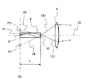
実施の形態1. 図1は本実施の形態に係る光学装置の構成を示す概略図である。本光学装置は光を放射する1次光源である光源手段1、反射面形状が回転2次曲面からなる反射ミラー20と略平行光束を収束するコンデンサーレンズ(第2のレンズ手段)21から構成される集光手段2、断面が四角形のミキシングロッド(均一化手段)3、少なくとも1枚のレンズから構成される第1のレンズ手段4、以下に説明する反射光学素子5により構成される照明装置であり、照明装置の光軸70外に配置された被照明面6(例えば、DMD等のライトバルブの画像表示面)を照明する。
【0032】
図1を用いて本光学装置の動作を説明する。図1において、光源1から放射された光は回転放物面からなる反射ミラー20で略平行光束11に変換され、後方のコンデンサーレンズ21によって収束光束12となる。この収束光束12の光束径が最も小さくなる位置付近では光源1の像(即ち、2次光源)が形成される。次に、この2次光源が形成される位置の近傍に、ミキシングロッド3の入射端面31を配置する。このときミキシングロッド3は反射ミラー20の回転軸とコンデンサーレンズ21の中心軸によって規定される照明光軸70とロッドの長軸が一致するように配置される。
【0033】
ミキシングロッド3に入射した光は側面での全反射を繰り返しながらその内部を伝播し、出射端面32から出射し発散光束13となる。また、ミキシングロッド3後方の第1のレンズ手段4は、ミキシングロッド3の出射端面32の像を照明光軸70上に設定された仮想被照明面60上に結像するように配置されている。なお、簡単のために、本実施の形態においては、第1のレンズ手段4が1枚構成のレンズによりなる場合について説明する。
【0034】
5は上記反射光学素子であり、第1のレンズ手段4によって形成される照明光束14を被照明面6の方向、すなわち光軸71に沿った方向へ偏向し、さらに光軸71から所定の角度傾いた法線72を有する矩形の被照明面6へ導く。このとき、照明光軸70と照明光軸71のなす角度が被照明面の法線72と照明光軸71のなす角度と一致するように反射光学素子が配置される。このような場合、被照明面6は仮想被照明面60と同様に、ミキシングロッド3の出射端面32と相似な矩形の光束により効率よく照明される。
【0035】
さらに詳しく本光学装置の動作について説明する。図2はミキシングロッド3によって生じる仮想的な2次光源について説明する概略図である。図2において、点Pは2次光源、S0は仮想2次光源が形成される面、P1、P2は仮想的な2次光源、33、34は仮想2次光源P1とP2からそれぞれミキシングロッド3の出射端面32へ到達する仮想的な光線、130、131は仮想2次光源P1、P2によって生じる実際の発散光線を示している。また、Lはミキシングロッド3の長さを示している。その他の符号は図1と同様であるので説明を省略する。
【0036】
まず、点Pに形成される2次光源から出射した光線は、ミキシングロッド3の側面を全反射しながら伝播し、発散光線130、131となって第1のレンズ手段4に入射する。ミキシングロッド3は透明なガラスやプラスチックなどの均質な材料で構成されており、n>n0の関係を満たす媒質内に配置される。ここで、nはミキシングロッド3の屈折率、n0はミキシングロッド3が配置される媒質の屈折率である。なお、本実施の形態では、空気中(n0≒1)にミキシングロッド3が置かれているとする。
【0037】
このような屈折率の関係から、点Pに形成される2次光源から発した光線は、ミキシングロッド3と空気の界面で所定の回数だけ全反射を繰り返して伝播する。このとき、出射端面32の側からは、見かけ上光線33、34の延長上に存在する仮想2次光源P1ならびにP2から光が出射されているように観察される。同様の理由で図示した2点以外にも多数の仮想2次光源が面S0上に形成される。
【0038】
一方、ミキシングロッド3の出射端面32は、これらの多数の仮想2次光源から発せられた全ての光線が通過する開口となる。この出射端面32においては、多数の仮想2次光源からの光束が重畳され、強度均一性の高い矩形光源が形成されることになる。すなわち、ミキシングロッド3による光線のミキシングによれば、不均一な強度分布を持つ2次光源から均一性の高い矩形面光源を得ることができる。
【0039】
図3は前述の仮想2次光源とこれが結像して形成される3次光源群の関係を示す概略図である。図3において、10は2次光源、15は仮想2次光源のひとつ、100は3次光源群、50は反射光学素子5の微小反射面を、それぞれ示しており、その他の符号は図1と同様であるので説明を省略する。
【0040】
第1のレンズ手段4はミキシングロッド3の出射端面32に形成される矩形光源像を被照明面6に結像させる作用を有する。このとき、仮想2次光源15に対しても第1のレンズ手段4による結像関係が成立する。すなわち、第1のレンズ手段4全系の焦点距離と複数の仮想2次光源のそれぞれの関係から、3次光源群100が所定の位置に形成される。3次光源群100の位置付近には、それぞれの3次光源の大きさに対応した微小反射面50が配置され、入射する収束光束を被照明面6の方向に偏向する。3次光源面近傍では仮想2次光源からの光線が最も小さなスポットに収束しており、微小反射面で効率よく光線を偏向させることができる。このような微小反射面50が不連続に隣接配置され、全体として反射光学素子5の反射面を形成する。
【0041】
図3では、ひとつの仮想2次光源15とこれに対応する3次光源の結像関係と、微小反射面50によって光線が被照明面6に導かれるところを破線で示している。このようにしてミキシングロッド3の出射端面像は、複数の仮想2次光源と3次光源の関係に応じて、被照明面6においてそれぞれ独立に結像し重畳されることになる。
【0042】
図4は近軸結像関係を示す図であり、焦点距離fの第1のレンズ手段4による出射端面32と仮想被照明面60の結像関係、ならびに仮想2次光源像面S0と3次光源面S1の結像関係を示している。尚、それぞれの像高、あるいは物体高と配置は矢印で表現し、これらを前記説明と同じ符号で示している。
【0043】
さて、本来第1のレンズ手段4はミキシングロッド3の出射端面32と仮想被照明面60が結像関係にあるように配置されており、出射端面32と第1のレンズ手段4の距離をa1、第1のレンズ手段4と仮想被照明面60の距離をb1とする。一方、第1のレンズ手段4と仮想2次光源像面S0との距離をa2、これの像面すなわち3次光源面S1と第1のレンズ手段4の距離をb2とする。また、出射端面32から仮想2次光源面S0までの距離はミキシングロッド3の長さをL、屈折率をnとしてL/nで表すことができる。以上のことから次の(1)〜(4)式のような関係が成り立ち、式(4)から3次光源が形成される近軸配置(即ち、距離b2)を求めることができる。
【0044】
a1-1+b1-1=f-1 (1)
【0045】
a2-1+b2-1=f-1 (2)
【0046】
a2=L/n+a1 (3)
【0047】
(1)〜(3)式より、
【0048】
b2={a1・b1・(a1+L/n)}/{(a1+b1)・(a1+L/n)-a1・b1}(4)
【0049】
例えば、a1=50mm、b1=150mmとすると(1)式からf=37.5mm、さらに、n=1.52、L=60mmとすると式(4)からb2≒64.56mmとなる。また(3)式よりa2=89.47mmとなる。
【0050】
なお、第1のレンズ手段4は実際には複数枚構成のレンズで構成することが可能であり、この場合レンズ全系の内部に3次光源面が形成される可能性がある。しかし、上記結像関係から規定される3次光源面の位置を条件に含めることで、反射光学素子5の配置の妨げとならないように第1のレンズ手段4を設計することができる。
【0051】
また、上記の数値ではb1/a1=3であるので、ミキシングロッド3の対角長さの約3倍に相当する対角長さを持った相似形状の被照明面を照明するのに適している。このとき仮想2次光源の大きさに対する3次光源の大きさの比はb2/a2とほぼ等しくなり、上記数値の場合は約0.72倍と縮小像が形成されることがわかる。さらに、3次光源群は第1のレンズ手段4により収束され仮想被照明面60へ向かう収束光束中に形成されるため、全ての3次光源を含む実効的な3次光源面の大きさは第1のレンズ手段4の有効径よりも小さくなる。よって反射光学素子5をコンパクトに作成することができ、装置の小型化、軽量化に大きく寄与する。
【0052】
さて、実際の光学系では近軸領域から外れる光線が存在するが、上記結像関係が成立しない範囲については出射端面32の結像位置の調整が必要となる。図5は前記(1)〜(4)式から求まる3次光源面上に配置された反射光学素子5のうち、周辺部を構成する微小反射素子51と52によって反射される光線が点線で示された被照明面6へ導かれる様子を示す概略図である。図の配置のように、微小反射素子51と被照明面6の距離は、もう一方の微小反射素子52と被照明面6との距離より大きくなるため、微小反射素子51による出射端面32の像61は被照明面6より手前に、微小反射素子52による出射端面32の像62は被照明面6より奥に形成される。結果として、このような結像面のずれは照明効率を低減させることになる。
【0053】
上記の結像面の位置ずれは、複数の微小反射面が3次光源面上に配置され、各3次光源に対応して各反射面の偏向方向が設定されているため生じる現象である。例えば、反射光学素子5の代わりに単純な平面ミラーを所定の角度だけ光軸に対して傾けて挿入すると、それぞれの3次光源に対応する主光線は平面ミラーで反射された後、再び被照明面上で交差する。その結果、各照明面は被照明面上で重畳されるが、重畳照明面と被照明面は大きく傾き、均一照明の効果を得ることは困難となる。以上のことから、主光線の方向と各照明光束による出射端面像の位置を調整すること、すなわち各微小反射面の角度と位置及び反射面形状の最適化によって、被照明面を斜めから、かつ均一に照明するための最適な照明光束を形成することが可能である。
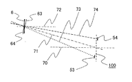
【0054】
図6は上記結像面の調整を行った微小反射光学素子の作用を説明する概略図である。微小反射面53と54による反射光の主光線をそれぞれ73、74とし、調整されたミキシングロッドの出射端面像をそれぞれ63、64とする。微小反射面53、54は調整のためにもともとの3次光源群100の面から離れた位置に配置されている。図に示されるように被照明面6から遠い微小反射面53は3次光源群100から被照明面6へ近づく方向に、逆に被照明面6に近い微小反射面54は被照明面6から遠ざかる方向へ調整される。一方、各微小反射面の角度により主光線が光軸72と交わる位置が調整されている。被照明面6の照明状態を観察、もしくは計算しながら以上のような調整を繰り返すことによって重畳照明光束の最適化を行うことができる。
【0055】
なお、3次光源の実効的な大きさを推定し、各微小反射面の大きさならびに配置を決定するには光線追跡による照明解析が有効である。まず、それぞれの3次光源に対して独立した解析を行い、全ての微小反射面による照明光束の重畳から被照明面の照明状態を推定する。そして、所望の照明特性が得られるまでこのような解析を繰り返せばよい。このとき微小反射面の形状は必ずしも平面である必要はなく、最適化のパラメータとして非球面、球面、不連続面などの面形状を用いても構わない。なお、反射光学素子全体としては反射面を規定する条件の下でいかなる形状も取ることができる。
【0056】
図7は最適設計された微小反射面による反射光学素子の具体的な構成例を示す概略図である。図において5は反射光学素子、55は微小反射面、56は最適設計の最小単位である微小反射体である。ある照明条件においてそれぞれ独立して最適化が施された微小反射面55が不連続に配列する素子として反射光学素子5を構成することができる。なお、最適設計の最小単位である微小反射体56の反射面、すなわち開口部の形状は図7のようにそれぞれ同じである必要はなく、またその大きさや配置も3次光源の特性に応じて様々な形態にすることが可能である。また、反射光学素子5は微小反射面55の精度を確保できる手法であればどのような成形法を用いてもよい。例えば、ガラスやプラスチック、セラミックなどの基材にアルミニウム等の金属薄膜や誘電体多層膜などの反射膜を成膜することで反射率の高い反射光学素子5を実現することができる。
【0057】
図8は反射光学素子5の具体的な構成の変形例を示す図である。図8において反射光学素子5は微小反射面55で構成される反射部と、基材部57から構成されており、大きさの異なる微小反射面55の組合わせによって反射面全体が構成されている。ミキシングロッド(均一化手段)の出射端面が矩形である場合、矩形の長辺方向と短辺方向で全反射の回数が異なる場合があり、3次光源の分布は中心点に関して対称とはならない。また、第1のレンズ手段が有するレンズ系の性能により3次光源群の形状も矩形から外側に歪んだ樽型になったり、逆に内側に歪んだ糸巻き型になったりするため、各微小反射面の配置や形状もこれに応じて設定する必要がある。なお、基材部57は反射光学素子5を保持するために設けているが、他の有効な保持方法を採用することによりこれを省略することも可能である。
【0058】
図9はxyz座標系における微小反射面55を示す概略図である。図9において75、76はそれぞれ微小反射面55への入射光線と反射光線を示しており、入射光線75とz軸は平行としている。また77は微小反射面55の法線であり、入射光線75となす角度はθであるとする。このとき反射光線76と微小反射面55の法線がなす角度もθとなる。
【0059】
78は入射光線75の延長線がxy平面と交わる点Qと原点Oを結んだ直線で、x軸となす角度をαとする。線78は反射光線76のxy平面への正射影と一致するので、z方向から全系を見れば微小反射面55に対してαの方向に被照明面が設定される。尚、図9には被照明面を図示していないが、被照明面とは、図1、図3などにて示す被照明面6と同様のものである。
【0060】
又、入射光線75の方向に対して反射させたい方向、すなわち角度2θが決まれば、微小反射面55を図のようにxy平面に対して角度θだけ傾ければよく、被照明面をxy平面と平行な平面に設定することで被照明面に対しては法線から2θの角度だけ傾いた方向から光線を入射させることができる。こうして全ての微小反射面に対して最適設計の初期値を求めることができる。
【0061】
例えば、反射光学素子5を前述のDMDの照明に適用した場合、照明光束に要求される条件は、DMDの法線に対する傾きが20度であること、かつ、DMDの法線回りのアジマス方向(図9においては、x軸と線78とのなす角αの方向)には、DMDの辺方向から45度回転した方向から入射する、ということである。よって、この図のような構成においては、α=45度、かつθ=10度とした微小反射面を初期値として用い、最適設計することが望ましい。
【0062】
以上のように、この反射光学素子5は、反射素子であるため熱の放散に優れるとともに、薄い平板形状に成形することができるのでさらに熱放散性に優れ、そのため、光束径が細く絞られたスポットに配置するにもかかわらず、熱破壊に強い素子として構成することができる。そして、このように反射光学素子5の耐熱性を高めることができるため、余分な冷却機構を省略することができ、軽量化、小型化に有利な装置を実現することができる。
【0063】
加えて、素子全体の厚さを部位によって著しく変化しないように設計することも可能であるため、熱変形にも強く、温度変化による光学性能劣化を最小限にとどめることが容易である。これらのことから、反射特性の向上や被照明面の均一照明に重点を置いた最適設計を行うことができ、設計の自由度も大きいという特徴がある。
【0064】
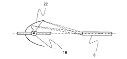
前述の説明からもわかるように、ミキシングロッド3の入射端面近傍に形成される2次光源の有効径が小さいほど光の利用効率を向上させることが容易であることが明らかであるが、集光方式は前述の回転放物面による反射ミラー20とコンデンサーレンズ21の組み合わせに限る必要はない。例えば、図10の光源装置は、キセノンランプやメタルハライドランプ、高圧水銀ランプなどの高輝度ランプ16から放射された光を回転楕円面鏡22で集光する方式であり、楕円面鏡22の第1焦点近傍に配置された高輝度ランプ16の発光部から出射した光が、楕円面鏡22の第2焦点近傍に配置されたミキシングロッド3の入射端面に到達するところを示している。さらに、図11には別の反射鏡の方式として直交放物面鏡(Orthogonal Parabolic Reflector;OPR)23を用いた例を示す。通常の放物面鏡は、焦点距離をfとした場合にその(x,y)断面が(5)式で与えられる曲線をx軸回りに回転して得られる曲面を反射面として用いる。
【0065】
y2=4fx
【0066】
一方、直交放物面鏡23は、(6)及び(7)式で与えられる曲線をY軸回りに回転した曲面を反射面として用いる。
【0067】
Y=2{f(f+X)}1/2 (但し、−f≦X≦0) (6)
【0068】
Y=2{f(f−X)}1/2 (但し、0≦X≦f) (7)
【0069】
図11において、17は線状光源、23は直交放物面鏡、Fは直交放物面鏡23の焦点位置である。直交放物面鏡23はY軸(即ち、回転軸)上に、略線状光源17(例えば、メタルハライドランプの放電アーク等)を配置して、略線状光源17の線方向と直角方向に出射する光線を焦点位置Fの一点に効率よく集光する作用がある。本発明においても、略線状光源17は直交放物面鏡23の回転軸上に配置することが望ましい。
【0070】
以上のように様々な集光方式が本発明に含まれるが、例えば主鏡と副鏡の組合わせにより反射鏡の開口方向に発散し利用されていなかった光を有効活用する方式や、部位によって異なる複数の回転2次曲面を連続的に繋ぎ合わせて反射面を構成し集光効率を向上させる方式なども勿論適用することができる。また指向性の強い光源を用いれば反射鏡そのものを省略する構成も可能である。具体的には発光ダイオードや面発光レーザなどの光源を用いることができ、ミキシングロッド3により均一性の高い面光源を得た後は、上記説明と同様の照明光学系を構成することによって類似の均一照明効果を得ることができる。
【0071】
本実施の形態では被照明面の形状を矩形とし、ミキシングロッド3の出射端面形状を重畳結像させ均一照明の効果を得る方式を説明した。しかし、ミキシングロッド3の代わりに円柱ロッドや楕円柱ロッド、その他さまざまな柱状ロッドを用いることにより所定の被照明領域を均一にかつ高効率に照明することが可能である。また、このようなロッドの全部あるいは一部分が先細あるいは逆に先太の形状をなし、入射端面と出射端面が異なる面積の相似形状となるように設定することも可能である。
【0072】
図12は出射側が大きくなる先太形状の矩形ロッド35を示す図である。図12では矢印で示すように内面で全反射する光線の平行度が高くなるが、反対に先細とすれば光線の平行度は低くなる。このようにロッドにテーパ角度を設定することにより、長方形の長辺方向と短辺方向で異なる平行度の調整を行なうこともでき、後段の第1のレンズ手段が有するレンズ系の作用と組合わせることで照明光学系の設計を多様化させることができる。勿論、このようなテーパ角度の設定によって3次光源の分布は等間隔に近い状態から大きく隔たることになる可能性が高いが、反射光学素子5を構成する微小反射面の最適化によって対応可能である。
【0073】
さらに、ミキシングロッド3の出射端面をロッドの長軸に垂直な平面からわずかに傾けて、出射端面の結像面と被照明面の角度の隔たりを予め低減させておくことも可能である。図13に示すように、出射端面が光軸に垂直でないロッド36から発散する光線は、矢印で示すように光軸79に関して非対称な分布となる。よって第1のレンズ手段41による結像作用によれば、ロッド36の出射端面の像66は光軸79に対して傾くことになる。なお、被照明面が要求する照明光の斜入射の効果を全てこのようなロッド出射端面の傾斜で行うのは困難である場合が多い。例えば、出射端面の傾斜が大きすぎると光線の傾きが大きくなりすぎるために、後段の第1のレンズ手段41の径を大きくしなければならず光学装置全体の容量を増加させなければならなくなる。そこで、ロッド36の入射端面も同様に光軸79に対して傾ければ、ロッド36の断面形状や長さの条件によれば上記光線の傾きを抑制できる可能性がある。本光学装置の反射光学素子5の作用を補い、かつ装置の小型化、軽量化に支障がない範囲で用いる分には、上記のような変形は非常に有効である。
【0074】
以上説明したように、本実施の形態によれば、ミキシングロッド側面での光の全反射に基づいて仮想的に形成される2次光源群が、第1のレンズ手段により結像して複数の3次光源が形成される。そして、この複数の3次光源の位置に対応して反射光学素子を配置しているため、所定の光束分布と強度分布を有する照明光束を効率よく反射して、被照明面にミキシングロッドの出射端面の像を結像し、上記の均一な強度分布の照明光束で被照明面を照明することができる。
【0075】
したがって、本発明に係る光源装置においては、簡単な構成で、被照明面の法線から所定の傾きを持った方向から照明光束を入射させ、この被照明面を均一に照明することができる。また、光源から出射される光を効率よく集光することができるので、光利用効率の高い光学装置を提供することができる。また、ミキシングロッドの出射端面を被照明面の形状と相似にした場合、光の損失を抑えて効率よく被照明面を照明する光学装置を提供することができる。さらにまた、ミキシングロッドは、入射端面あるいは出射端面の少なくとも一方がロッドの長軸に対して垂直な面から傾いて設定することも可能であるため、被照明面の斜方照明を目的とした反射光学素子の最適化において自由度の高い設計を行うことができる。また、反射光学素子による光路の折り曲げ方向の自由度が大きいため、全体としてコンパクトな光学装置を容易に実現することができる。
【0076】
実施の形態2. 本発明の実施の形態2に係るプロジェクタ装置の照明光学系について説明する。図14は反射型ライトバルブ65を用いたプロジェクタ装置の構成を示す概略図であり、実施の形態1で述べた光学装置を照明光学系に適用したものである。反射型ライトバルブ65は法線方向以外、すなわち斜め方向からの照明を要求するデバイスが望ましく、例えば従来例で説明したDMD(Digital Micromirror Device)が好適である。反射型ライトバルブ65に対向する位置には投写レンズ手段(第3のレンズ手段)8が配置され、図示しないスクリーン手段に反射型ライトバルブ65に形成される画像が拡大投写される。また、仮想2次光源15が第1のレンズ手段4によって3次光源18を形成し、反射型ライトバルブ65で反射された後、再び光源像19を形成するところを点線で示している。この光源像19は投写レンズ手段8の入射瞳81付近に形成され、高効率で照度均一性の高いプロジェクタ装置が構成される。なお、その他の符号は図1と同様であるので説明を省略する。
【0077】
さて、反射型ライトバルブ65が前述のDMDのように微小な反射ミラーで構成されている場合、入射する照明光束が発散性ならば反射したのち光変調された光束は、発散光束となって投写レンズ8に入射する。逆に、収束性の照明光束の場合は、反射型ライトバルブ65での反射後も収束性を保ちながら投写レンズ8に入射する。入射瞳上で3次光源群の像が過不足なく形成されるために図14に示すようにフィールドレンズ44を付加することも可能である。いずれにせよ、反射光学素子5の付近に形成される3次光源群が、再び投写レンズ8の瞳上で結像するために十分な瞳径を有し、適切な瞳位置を持つ投写レンズ8であればよい。
【0078】
主光線が光軸と平行になるテレセントリックレンズでは、射出瞳位置が無限遠で瞳径が無限大である。そのため、図14に示すように投写レンズ8内部の瞳位置に3次光源群が再結像するという状態にはならないが、テレセントリックに照明された反射型ライトバルブからの光を効率よく集光することができる。このようにプロジェクタ装置として所定の光学性能を発揮するものであれば、様々なタイプの投写レンズ8を用いることができる。
【0079】
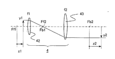
本実施の形態によるプロジェクタ装置において、いわゆる照明光学系の最も大きな特徴は、ミキシングロッド3による2次的な平面光源を反射型ライトバルブ65に結像する結像光学系が構成される点である。これまでの説明で1枚のレンズに代表されて描かれている第1のレンズ手段4の構成については、反射型ライトバルブ65が要求する照明条件を満たし、かつ反射光学素子5を挿入する空間的余裕が確保されることが最低限必要である。例えば、図15に示すアフォーカル系(afocal系:無限焦点系)は無限遠の物体に対しては無限遠像となるが、有限距離の物体に対しては有限位置に像を作るので第1のレンズ手段4に適用することができる。図15によりアフォーカル系の結像関係を説明する。
【0080】
第1レンズ42の物体側焦点Ff1より距離z1だけ後方の位置にあるミキシングロッド3の出射端面が、最終的に第2レンズ43の像側焦点Fb2より距離z2だけ後方の位置に結像するとすれば、次の式(8)、(9)が成り立つ。
【0081】
z2=−f22/z1=(f2/f1)2・z1=z1/m2 (8)
【0082】
β=(f1/z1)・(-z2/f2)=-(f1/f2)・(1/m2)=1/m (9)
【0083】
ここで、mはアフォーカル倍率(=−f1/f2)、βは横倍率であり、このアフォーカル倍率mは、ミキシングロッドの出射端面と反射型ライトバルブの画像表示面の大きさから決まる結像倍率にほぼ合致するように設定される。尚、f1、f2はそれぞれ第1、第2レンズ42、43の焦点距離である。
【0084】
よって、式(8)から求まる像位置z2に反射型ライトバルブ65を配置すれば、像倍率は物体像位置とは無関係に設定できるので、ミキシングロッド3の出射端面像を所望の大きさに拡大、あるいは縮小結像する際に光学系を構成する自由度が高くなる。また、アフォーカル系に入射する光線が光軸に平行であれば出射光線もまた光軸に平行であるので、ミキシングロッド出射端面から発散する全ての光線を効率よく被照明面に導くのに適した光学系であると言える。
【0085】
勿論、図15で説明したアフォーカル系は基本的な構成であり、実際には上記第1レンズ42ならびに第2レンズ43がそれぞれ複数のレンズから構成される第1レンズ群、第2レンズ群を形成し、それぞれの焦点を共有する構成となっていても構わない。いずれの場合でも3次光源は第1レンズ群あるいは第2レンズ群の設定にしたがって所定の位置に形成されるため、反射光学素子5のアフォーカル系内への挿入、ならびに反射光束と第1のレンズ手段4の干渉の回避を条件にして、照明光学系を最適化する必要がある。反射光束と第1のレンズ手段4の干渉を回避するためにレンズだけでなく反射ミラー等を光路中に挿入することも勿論可能である。
【0086】
また、プロジェクタ装置は小型化の目的のため、構成要素の配置を工夫したコンパクトな光路を求められることが多い。図16はプロジェクタ装置の構成を示す変形例である。符号は図14と共通であるので説明は省略する。図14では照明光学系の光軸70と反射型ライトバルブ65の法線72がほぼ平行となる配置であったが、本変形例では両者がほぼ直交するような配置となっている。反射型ライトバルブ65が要求する照明条件を満たす照明光学系であれば図16のように光軸が立体的に交差する構成を採ることは勿論構わない。
【0087】
また、実施の形態1で説明した全ての照明光学系ならびにその変形例を、実施の形態2である本プロジェクタ装置に適用可能であることは言うまでもない。
【0088】
実施の形態3. 本発明の実施の形態3に係るマルチDMDプロジェクタ装置について説明する。図17は本発明に係る光学装置を具備し、DMDを反射型ライトバルブとした4台のフロントプロジェクタ装置を用いて、マルチ(例えば、本実施の形態においては4画面)画面のプロジェクタ装置を構成したところを示している。図において、90はマルチリアプロジェクタ装置、91〜94はフロントプロジェクタ装置、95はリアスクリーンである。なお、フロントプロジェクタ装置91〜94については内部の構成を省略するが、本発明の反射光学素子を内包し、明るさの均一性に優れた投写画面を提供することができるのは前述の通りである。
【0089】
マルチリアプロジェクタ装置90は画面数や内部構成など様々な形態を取り得るが、ここでは最も単純な構成のもので説明する。各フロントプロジェクタ装置はリアスクリーン95上に目地なしで投写すべく隣接する投写画像の境界がほぼ一致するように配置され調整されているものとする。スクリーン95には便宜上の単位画面の境界線を点線で示している。
【0090】
実際のマルチ画面においては、単位画面間の目地にあたる部分がもっとも画像の品質を低減させる要因となる。さらに目地を挟んで両側の明るさに差が生じたり、目地に沿ってむらがあったりすると非常に見苦しい画面となる。そのため、実際には明るさや色調が近い角を画面中央に集めるように各プロジェクタ装置の配置を入れ替えたりすることでわずかに調子を整え、比較的むらを目立たなくさせることができる。しかし、単位画面の対角線方向に明るさのむらが生じると上記調整は非常に難しくなる。また、このような調整もマルチ画面数が増大するにつれ困難になる。したがって、単位画面に生じる上記明るさむらを低減することは、マルチ画面の画質向上にも重要である。
【0091】
このように、ひとつの筐体が複数のプロジェクタ装置を内包する形態に限らず、各々投写光学系を内蔵した複数の筐体を縦横に所定数配列することにより大画面のマルチプロジェクタ装置を構成しても良い。この場合には、それぞれの投写光学系に対応するスクリーン手段が共用されて配置されるか、もしくは各筐体毎に別個にスクリーン手段が設けられるかの形態が取られる。
【0092】
本発明の光学装置による照明光学系を具備するフロントプロジェクタ装置91〜94によれば、このような画面対角線方向の明るさむらを低減させることができ、単位プロジェクタ装置(あるいは、リアプロジェクタ装置)の配置の自由度を高め、最終画面の画質を向上させることが可能となる。このような効果はマルチの画面数やスクリーンの種類、またプロジェクタ装置90の内部構成に直接影響を受けないので、所望の大きさ、画面数のマルチプロジェクタ装置を構成することができ、例えば装置の奥行き低減のために各フロントプロジェクタ装置とスクリーン95間に反射ミラーが挿入されるような構成をはじめ、種々の構成に対して同様の効果を得ることが可能である。即ち、筐体内部には、目的に応じて画像反転あるいは筐体寸法低減を可能な反射手段を配置しても良い。
【0093】
なお、本発明は上記の実施の形態に限定されるものではなく、本発明の目的を逸脱せず、その要旨を変更しない範囲において様々な変形例が可能であることも勿論である。
【0094】
【発明の効果】
本発明に係る光源装置は、1次光源である光源手段と、該光源手段からの出射光を集光して2次光源を形成する集光手段と、入射端面が前記2次光源の形成される位置近傍に配置され、出射端面から均一性の高い強度分布を有する発散光束を出射する均一化手段と、前記均一化手段の出射光を集光して、光路中に複数の3次光源を形成する第1のレンズ手段と、前記複数の3次光源の形成される位置近傍に配置され、前記第1のレンズ手段の出射光を所望の方向へ反射する反射光学素子とを備えたので、被照明面の法線方向に対して所定の傾きを持った方向から照明光束を入射させた場合に、前記均一化手段の出射端面の像が形成される位置近傍に配置された被照明面において、均一かつ対称性に優れた照度分布を得ることができるという効果を奏する。
【図面の簡単な説明】
【図1】 実施の形態1に係る光学装置の構成を示す概略図。
【図2】 仮想2次光源について説明する概略図。
【図3】 仮想2次光源と3次光源群の関係を示す概略図。
【図4】 近軸結像関係を示す概念図。
【図5】 微小反射素子と被照明面の関係を示す概略図。
【図6】 微小反射光学素子の作用を説明する概略図。
【図7】 反射光学素子の具体な構成例を示す概略図。
【図8】 反射光学素子の具体的な構成の変形例を示す概略図。
【図9】 xyz座標系における微小反射面を示す概略図。
【図10】 楕円面鏡を用いた照明光学系の変形例を示す図。
【図11】 直交放物面鏡の作用を示す概略図。
【図12】 先太形状の矩形ロッドを示す図。
【図13】 出射端面が光軸に垂直でないロッドを示す図。
【図14】 実施の形態2に係るプロジェクタ装置の構成を示す概略図。
【図15】 アフォーカル系の作用を示す概略図。
【図16】 本発明に係るプロジェクタ装置の変形例の構成を示す概略図。
【図17】 本発明に係るマルチプロジェクタ装置の構成を示す概略図。
【図18】 DMD2ピクセルの構成を示す斜視図。
【図19】 DMDの表示原理を説明する概念図。
【図20】 従来のカラー画像表示装置を示す模式的構成図
【図21】 照明されたDMDを模式的に示す図。
【図22】 ミキシングロッドを用いた照明光学系の概念図。
【符号の説明】
1 光源手段、 2 集光手段、 3 ミキシングロッド(均一化手段)、
4 第1のレンズ手段、 5 反射光学素子、 6 被照明面、
8 投写レンズ(第3のレンズ手段)、 10 2次光源、
11 略平行光束、 12 収束光束、 13 発散光束、
14 照明光束、 15 仮想2次光源、 16、17 高輝度ランプ、
18 3次光源、 19 光源像、 20 反射ミラー、
21 コンデンサーレンズ(第2のレンズ手段)、 22 回転楕円面鏡、
23 直交放物面鏡、 31 入射端面、 32 出射端面、
33、34 仮想的な光線、 35 先太形状の矩形ロッド、
36 所定の傾きを有するロッド、 41 第1のレンズ手段、
42 第1レンズ、 43 第2レンズ、 44 フィールドレンズ、
50〜55 微小反射面、 56 微小反射体、 57 基材部、
60 仮想被照明面、 61〜64 出射端面の像、
65 反射型ライトバルブ、 66 出射端面の像、 70 光軸、
71 光軸、 72 法線、 73、74 反射光の主光線、
75 入射光線、 76 反射光線、 77微小反射面の法線、
78 点Qと点Oを結ぶ線、 79 光軸、 80 投写レンズ、
81 瞳、 90 マルチリアプロジェクタ装置、
91〜94 フロントプロジェクタ装置、 95 マルチスクリーン、
100 3次光源群、 130、131 発散光線、
150〜152 光源、 200 反射鏡、 300 ミキシングロッド、
400 光学薄膜、 401 レンズ、
510〜516 マイクロミラー、 600、601 DMD素子、
602 光アブソーバ、 603、604 DMD素子、
605 ライトバルブ、 800 結像レンズ、 900 スクリーン、
C 微小反射面と線分78との交点、 Ff1 第1レンズの物体側焦点、
Fb1 第1レンズの像側焦点、 Ff2 第2レンズの物体側焦点、
Fb2 第2レンズの像側焦点、 L ミキシングロッドの長さ、
O xyz座標系の原点、 P 2次光源、 P1、P2 仮想2次光源、
Q 入射光線とxy平面との交点、 S0 仮想2次光源が形成される面、
a1 出射端面と第1のレンズ手段の距離、
a2 第1のレンズ手段と仮想2次光源面との距離、
b1 第1のレンズ手段と仮想被照明面、
b2 3次光源面と第1のレンズ手段との距離、
f1 第1レンズの焦点距離、 f2 第2レンズの焦点距離、
y1 第1レンズの物体側焦点から距離z1だけ後方の位置における像高、
y2 第2レンズの像側焦点から距離z2だけ後方の位置における像高、
α 線78とx軸とのなす角、 α1 光源のミラーに対する設置角度、
θ 入射光線、反射光線と法線とのなす角、 θ1 ミラーの傾斜角度。[0001]
BACKGROUND OF THE INVENTION
The present invention relates to an optical device, and a projector device, a rear projector device, and a multi-projector device using the optical device.
[0002]
[Prior art]
In recent years, projector devices have attracted attention as large-screen image display devices. A compact, high-definition, high-luminance CRT projector device using a CRT, a liquid crystal projector device using a liquid crystal panel, a DMD projector device using a DMD (Digital Micromirror Device), and the like have been commercialized. Among them, DMD is a digital drive element, so it is in principle compatible with computer information display and digital television broadcasting, and is one of the most promising light valves for projector devices.
[0003]
First, the structure of the DMD will be described. DMD uses semiconductor manufacturing technology to arrange a large number of micromirrors of 16 μm × 16 μm, for example, on a silicon substrate, and controls the reflection direction of incident light for each mirror by electrically controlling them. A minute mirror corresponds to a pixel, and image information is displayed by projecting onto a screen via a projection lens. FIG. 18 is a perspective view showing a configuration of a 2-pixel DMD element. In the figure,
[0004]
Aluminum is vapor-deposited on the surfaces of the
[0005]
Next, the principle of the optical system of a video projector using DMD as a light valve will be described with reference to FIG. FIG. 19 is a conceptual diagram for explaining the principle of DMD display by a single-plate DMD projector apparatus, in which 150 is a light source such as a metal halide lamp, 601 is a DMD, of which 512 and 513 are micromirrors rotated by +10 degrees, and 514 is − The micromirror rotated by 10 degrees is enlarged and conceptually shown.
[0006]
As is apparent from the DMD operating principle described above, the most characteristic condition for illuminating the DMD is that illumination light must be incident at a predetermined angle from the normal direction of the illuminated surface. That is. FIG. 20 is a schematic configuration diagram showing a conventional color image display device that displays a color image using a DMD, and is disclosed in, for example, Japanese Patent Laid-Open No. 10-039240. In FIG. 20, 603 is a DMD, 515 and 516 are micromirrors constituting the DMD, 151 is a parallel white light source that emits parallel white light, 400 is an optical thin film that generates transmitted light of a specific wavelength corresponding to the incident angle,
[0007]
The most notable here is the arrangement of the parallel
[0008]
The illumination light distribution on the illuminated surface is not concentric when the illuminated surface is illuminated from a direction inclined from its normal by an illumination beam having an intensity distribution that is concentric, that is, rotationally symmetric with respect to the optical axis. it is obvious. FIG. 21 schematically shows a
[0009]
In the case of a DMD projector device, it is relatively easy to reduce the illumination unevenness as described above by digital signal processing. That is, the projection light intensity for each pixel may be normalized so that the entire screen has a uniform illuminance distribution with reference to the pixel to which the illumination light with the lowest intensity is incident. However, improvement in image quality by such a light reduction process is not desirable from the viewpoint of light utilization efficiency. In addition, since DMD is a reflection type light valve, it has an advantage of being relatively resistant to heat as compared with a transmission type light valve, and uses a high output light source such as a xenon lamp or a metal halide lamp of several hundred to two or three kW class. It is possible. However, as with other projector devices using light valves, the rate at which the light source light finally reaches the screen, that is, the light utilization efficiency, is only about a few percent. Therefore, in order to improve the light use efficiency in each component, reduction of illumination unevenness by the optical system has been an important issue.
[0010]
Accordingly, in order to improve the illumination uniformity of the light valve, for example, an illumination optical system using a mixing rod or the like is used in a conventional projector apparatus.
[0011]
FIG. 22 is a conceptual diagram of an illumination optical system using a mixing rod having a rectangular input / output end face. 152 is a light source, 200 is a reflecting mirror, 300 is a mixing rod, 401 is a lens, and 605 is a light valve. The light generated from the
[0012]
The uniform illumination method using the mixing rod as described above can obtain the maximum effect when the light valve (that is, the surface to be illuminated) is arranged perpendicular to the illumination optical axis. However, even if, for example, a plane mirror is arranged in the illumination optical path and the illumination light beam is incident on the DMD from a predetermined direction, the angle of the exit end face image of the mixing rod and the DMD surface does not coincide with each other, and uneven illumination occurs. The problem that is unavoidable occurs.
[0013]
[Problems to be solved by the invention]
In view of the above-described problems, the present invention makes illumination light incident from a direction having a predetermined inclination with respect to the normal direction of the surface to be illuminated with respect to oblique illumination in an arbitrary plane represented by the illumination of the DMD. The present invention also provides an optical device that can obtain a uniform and excellent illuminance distribution on the surface to be illuminated, and a projector device, a rear projector device, and a multi-projector device using the same.
[0014]
In particular, in a multi-projector device in which a large screen is configured by arranging a plurality of projector devices (or rear projector devices) vertically and horizontally, not only the improvement of light utilization efficiency but also the difference in brightness and color between the screens, especially It is strictly required to minimize the difference between brightness and color in the vicinity of the boundaries of the arranged projection screens and make the screen joints inconspicuous. Therefore, in the projection screen of each unit projector device (or rear projector device), there is a problem that brightness and color uniformity must be maximized and the illumination unevenness must be removed.
[0015]
[Means for Solving the Problems]
The light source device according to the present invention includes a light source unit that is a primary light source, a condensing unit that condenses light emitted from the light source unit to form a secondary light source, and an incident end surface of the secondary light source. Near the position , Out From the end face A divergent light beam with a highly uniform intensity distribution Uniform means for emitting, first lens means for condensing the emitted light from the uniformizing means to form a plurality of tertiary light sources in the optical path, and the vicinity of positions where the plurality of tertiary light sources are formed And a reflective optical element that reflects the light emitted from the first lens means in a desired direction.
[0031]
DETAILED DESCRIPTION OF THE INVENTION
Embodiment 1 FIG. FIG. 1 is a schematic diagram showing a configuration of an optical device according to the present embodiment. This optical apparatus is composed of a light source means 1 that is a primary light source that emits light, a
[0032]
The operation of this optical apparatus will be described with reference to FIG. In FIG. 1, the light emitted from the light source 1 is converted into a substantially
[0033]
The light incident on the mixing
[0034]
5 is the reflection optical element, which deflects the
[0035]
The operation of this optical apparatus will be described in more detail. FIG. 2 is a schematic diagram for explaining a virtual secondary light source generated by the mixing
[0036]
First, the light beam emitted from the secondary light source formed at the point P propagates while totally reflecting the side surface of the mixing
[0037]
Due to such a refractive index relationship, the light beam emitted from the secondary light source formed at the point P propagates by repeating total reflection a predetermined number of times at the interface between the mixing
[0038]
On the other hand, the emission end face 32 of the mixing
[0039]
FIG. 3 is a schematic diagram showing the relationship between the above-described virtual secondary light source and a tertiary light source group formed by forming an image thereof. In FIG. 3, 10 is a secondary light source, 15 is one of virtual secondary light sources, 100 is a tertiary light source group, and 50 is a micro-reflecting surface of the reflective
[0040]
The first lens means 4 has a function of forming a rectangular light source image formed on the emission end face 32 of the mixing
[0041]
In FIG. 3, an image forming relationship between one virtual secondary
[0042]
FIG. 4 is a diagram showing a paraxial imaging relationship. The imaging relationship between the
[0043]
The first lens means 4 is originally arranged so that the emission end face 32 of the mixing
[0044]
a1 -1 + B1 -1 = F -1 (1)
[0045]
a2 -1 + B2 -1 = F -1 (2)
[0046]
a2 = L / n + a1 (3)
[0047]
From equations (1) to (3),
[0048]
b2 = {a1 · b1 · (a1 + L / n)} / {(a1 + b1) · (a1 + L / n) −a1 · b1} (4)
[0049]
For example, if a1 = 50 mm and b1 = 150 mm, f = 37.5 mm from the equation (1), and if n = 1.52 and L = 60 mm, then b2≈64.56 mm from the equation (4). Further, from the expression (3), a2 = 89.47 mm.
[0050]
Note that the first lens means 4 can actually be composed of a plurality of lenses, and in this case, a tertiary light source surface may be formed inside the entire lens system. However, the first lens means 4 can be designed so as not to hinder the arrangement of the reflective
[0051]
Moreover, since b1 / a1 = 3 in the above numerical values, it is suitable for illuminating a similar surface to be illuminated having a diagonal length corresponding to about three times the diagonal length of the mixing
[0052]
Now, in an actual optical system, there are light rays that deviate from the paraxial region, but it is necessary to adjust the imaging position of the emission end face 32 in the range where the imaging relationship is not established. FIG. 5 shows the light rays reflected by the
[0053]
The positional shift of the imaging surface is a phenomenon that occurs because a plurality of minute reflecting surfaces are arranged on the tertiary light source surface and the deflection direction of each reflecting surface is set corresponding to each tertiary light source. For example, when a simple plane mirror is inserted at an angle with respect to the optical axis instead of the reflective
[0054]
FIG. 6 is a schematic diagram for explaining the operation of the micro-reflection optical element in which the image plane is adjusted. The principal rays of the reflected light from the
[0055]
Illumination analysis by ray tracing is effective in estimating the effective size of the tertiary light source and determining the size and arrangement of each minute reflecting surface. First, independent analysis is performed for each tertiary light source, and the illumination state of the illuminated surface is estimated from the superimposition of illumination light beams by all the micro-reflecting surfaces. Then, such analysis may be repeated until a desired illumination characteristic is obtained. At this time, the shape of the minute reflecting surface is not necessarily a flat surface, and a surface shape such as an aspherical surface, a spherical surface, or a discontinuous surface may be used as an optimization parameter. The entire reflecting optical element can take any shape under conditions that define the reflecting surface.
[0056]
FIG. 7 is a schematic view showing a specific configuration example of a reflective optical element with an optimally designed minute reflecting surface. In the figure, 5 is a reflective optical element, 55 is a micro-reflecting surface, and 56 is a micro-reflector which is the minimum unit of optimum design. The reflective
[0057]
FIG. 8 is a diagram showing a modification of the specific configuration of the reflective
[0058]
FIG. 9 is a schematic diagram showing the
[0059]
[0060]
If the direction to be reflected with respect to the direction of the
[0061]
For example, when the reflective
[0062]
As described above, since this reflective
[0063]
In addition, since it is possible to design the thickness of the entire element so as not to change significantly depending on the part, it is resistant to thermal deformation and it is easy to minimize optical performance deterioration due to temperature changes. For these reasons, it is possible to perform an optimum design with an emphasis on improvement of reflection characteristics and uniform illumination of a surface to be illuminated, and there is a feature that the degree of freedom of design is large.
[0064]
As can be seen from the above description, it is clear that the light utilization efficiency is easier to improve as the effective diameter of the secondary light source formed near the incident end face of the mixing
[0065]
y 2 = 4fx
[0066]
On the other hand, the orthogonal
[0067]
Y = 2 {f (f + X)} 1/2 (However, -f≤X≤0) (6)
[0068]
Y = 2 {f (f−X)} 1/2 (However, 0 ≦ X ≦ f) (7)
[0069]
In FIG. 11, 17 is a linear light source, 23 is an orthogonal parabolic mirror, and F is a focal position of the orthogonal
[0070]
As described above, various condensing methods are included in the present invention. For example, depending on a method or a part for effectively using light that has been diverged in the opening direction of the reflecting mirror by a combination of the primary mirror and the secondary mirror, Of course, a system in which a plurality of different rotating quadratic surfaces are continuously connected to form a reflecting surface to improve the light collection efficiency can also be applied. If a light source with strong directivity is used, a configuration in which the reflecting mirror itself is omitted is also possible. Specifically, a light source such as a light-emitting diode or a surface-emitting laser can be used. After obtaining a highly uniform surface light source by the mixing
[0071]
In the present embodiment, a method has been described in which the shape of the surface to be illuminated is rectangular, and the shape of the exit end surface of the mixing
[0072]
FIG. 12 is a view showing a thick
[0073]
Further, it is possible to slightly reduce the angle difference between the imaging surface of the emission end surface and the illumination target surface by slightly inclining the emission end surface of the mixing
[0074]
As described above, according to the present embodiment, the secondary light source group that is virtually formed based on the total reflection of the light on the side surface of the mixing rod is imaged by the first lens unit and a plurality of light sources are formed. A tertiary light source is formed. Since the reflecting optical elements are arranged corresponding to the positions of the plurality of tertiary light sources, the illumination light beam having a predetermined light beam distribution and intensity distribution is efficiently reflected and emitted from the mixing rod to the surface to be illuminated. An image of the end face can be formed and the surface to be illuminated can be illuminated with the illumination light beam having the uniform intensity distribution.
[0075]
Therefore, in the light source device according to the present invention, the illumination light beam can be incident from a direction having a predetermined inclination from the normal line of the illuminated surface with a simple configuration, and the illuminated surface can be illuminated uniformly. Moreover, since the light emitted from the light source can be collected efficiently, an optical device with high light utilization efficiency can be provided. In addition, when the exit end face of the mixing rod is similar to the shape of the surface to be illuminated, it is possible to provide an optical device that efficiently illuminates the surface to be illuminated while suppressing light loss. Furthermore, since the mixing rod can be set so that at least one of the incident end surface and the output end surface is inclined from a plane perpendicular to the long axis of the rod, the reflection is intended for oblique illumination of the illuminated surface. It is possible to design with a high degree of freedom in optimizing optical elements. In addition, since the degree of freedom in the direction of bending the optical path by the reflective optical element is large, a compact optical device as a whole can be easily realized.
[0076]
[0077]
Now, when the
[0078]
In a telecentric lens in which the principal ray is parallel to the optical axis, the exit pupil position is infinite and the pupil diameter is infinite. For this reason, as shown in FIG. 14, the tertiary light source group does not re-image at the pupil position inside the
[0079]
In the projector device according to the present embodiment, the most significant feature of the so-called illumination optical system is that an imaging optical system for forming an image on the
[0080]
The exit end face of the mixing
[0081]
z2 = −f2 2 / Z1 = (f2 / f1) 2 ・ Z1 = z1 / m 2 (8)
[0082]
β = (f1 / z1) · (−z2 / f2) = − (f1 / f2) · (1 / m 2 ) = 1 / m (9)
[0083]
Here, m is an afocal magnification (= −f1 / f2), β is a lateral magnification, and this afocal magnification m is determined by the size of the emission end face of the mixing rod and the image display surface of the reflective light valve. It is set so as to substantially match the image magnification. Note that f1 and f2 are focal lengths of the first and
[0084]
Therefore, if the reflection type
[0085]
Of course, the afocal system described with reference to FIG. 15 has a basic configuration. In practice, the first lens group and the second lens group are each composed of a plurality of lenses. They may be formed and share their respective focal points. In any case, since the tertiary light source is formed at a predetermined position in accordance with the setting of the first lens group or the second lens group, the reflection
[0086]
In addition, for the purpose of miniaturization, projector apparatuses often require a compact optical path with a devised arrangement of components. FIG. 16 is a modification showing the configuration of the projector apparatus. The reference numerals are the same as those in FIG. In FIG. 14, the
[0087]
Needless to say, all the illumination optical systems described in the first embodiment and modifications thereof can be applied to the projector apparatus according to the second embodiment.
[0088]
[0089]
The
[0090]
In an actual multi-screen, the portion corresponding to the joint between unit screens is the factor that most reduces the image quality. Furthermore, if there is a difference in brightness on both sides across the joint, or if there is unevenness along the joint, the screen becomes very unsightly. Therefore, in actuality, it is possible to slightly adjust the tone by changing the arrangement of the projector devices so that the corners with similar brightness and color tone are gathered at the center of the screen, and relatively unevenness can be made inconspicuous. However, if uneven brightness occurs in the diagonal direction of the unit screen, the above adjustment becomes very difficult. Such adjustment also becomes difficult as the number of multi-screens increases. Therefore, reducing the brightness unevenness generated on the unit screen is also important for improving the image quality of the multi-screen.
[0091]
In this way, not only is a configuration in which a single housing contains a plurality of projector devices, but a large-screen multi-projector device is configured by arranging a predetermined number of a plurality of housings each incorporating a projection optical system vertically and horizontally. May be. In this case, the screen means corresponding to each projection optical system is shared and arranged, or the screen means is separately provided for each housing.
[0092]
According to the
[0093]
It should be noted that the present invention is not limited to the above-described embodiment, and various modifications may be made without departing from the object of the present invention and without changing the gist thereof.
[0094]
【The invention's effect】
The light source device according to the present invention includes a light source unit that is a primary light source, a condensing unit that condenses light emitted from the light source unit to form a secondary light source, and an incident end surface of the secondary light source. Near the position , Out From the end face A divergent light beam with a highly uniform intensity distribution Uniform means for emitting, first lens means for condensing the emitted light from the uniformizing means to form a plurality of tertiary light sources in the optical path, and the vicinity of positions where the plurality of tertiary light sources are formed And a reflecting optical element that reflects the light emitted from the first lens means in a desired direction, so that the illumination light flux is emitted from a direction having a predetermined inclination with respect to the normal direction of the surface to be illuminated. In the case of incidence, there is an effect that a uniform and excellent illuminance distribution can be obtained on the illuminated surface arranged near the position where the image of the exit end face of the uniformizing means is formed.
[Brief description of the drawings]
FIG. 1 is a schematic diagram illustrating a configuration of an optical device according to a first embodiment.
FIG. 2 is a schematic diagram illustrating a virtual secondary light source.
FIG. 3 is a schematic diagram showing a relationship between a virtual secondary light source and a tertiary light source group.
FIG. 4 is a conceptual diagram showing a paraxial imaging relationship.
FIG. 5 is a schematic view showing a relationship between a minute reflecting element and an illuminated surface.
FIG. 6 is a schematic diagram for explaining the operation of a minute reflection optical element.
FIG. 7 is a schematic diagram illustrating a specific configuration example of a reflective optical element.
FIG. 8 is a schematic diagram showing a modification of the specific configuration of the reflective optical element.
FIG. 9 is a schematic view showing a minute reflecting surface in an xyz coordinate system.
FIG. 10 is a view showing a modification of the illumination optical system using an ellipsoidal mirror.
FIG. 11 is a schematic diagram showing the operation of an orthogonal parabolic mirror.
FIG. 12 is a view showing a thick rectangular rod.
FIG. 13 is a view showing a rod whose exit end face is not perpendicular to the optical axis.
FIG. 14 is a schematic diagram showing a configuration of a projector apparatus according to a second embodiment.
FIG. 15 is a schematic diagram showing the action of an afocal system.
FIG. 16 is a schematic diagram showing a configuration of a modified example of the projector device according to the invention.
FIG. 17 is a schematic diagram showing a configuration of a multi-projector device according to the present invention.
FIG. 18 is a perspective view showing a configuration of a DMD2 pixel.
FIG. 19 is a conceptual diagram illustrating the display principle of DMD.
FIG. 20 is a schematic configuration diagram showing a conventional color image display device.
FIG. 21 is a diagram schematically illustrating an illuminated DMD.
FIG. 22 is a conceptual diagram of an illumination optical system using a mixing rod.
[Explanation of symbols]
1 light source means, 2 light collecting means, 3 mixing rod (homogenizing means),
4 first lens means, 5 reflective optical element, 6 illuminated surface,
8 projection lens (third lens means), 10 secondary light source,
11 substantially parallel light beam, 12 convergent light beam, 13 divergent light beam,
14 illumination light flux, 15 virtual secondary light source, 16, 17 high-intensity lamp,
18 tertiary light source, 19 light source image, 20 reflecting mirror,
21 condenser lens (second lens means), 22 spheroidal mirror,
23 orthogonal parabolic mirrors, 31 entrance end face, 32 exit end face,
33, 34 hypothetical rays, 35 thick rectangular rod,
36 a rod having a predetermined inclination; 41 first lens means;
42 first lens, 43 second lens, 44 field lens,
50-55 micro reflective surface, 56 micro reflector, 57 base material part,
60 virtual illuminated surfaces, 61-64 images of exit end faces,
65 reflection type light valve, 66 image of emission end face, 70 optical axis,
71 optical axis, 72 normal, 73, 74 principal ray of reflected light,
75 incident light beam, 76 reflected light beam, 77 normal of micro-reflecting surface,
78 Line connecting point Q and point O, 79 optical axis, 80 projection lens,
81 pupil, 90 multi-rear projector device,
91-94 Front projector device, 95 Multi-screen,
100 tertiary light source group, 130, 131 divergent light beam,
150-152 light source, 200 reflector, 300 mixing rod,
400 optical thin film, 401 lens,
510-516 micromirror, 600, 601 DMD element,
602 optical absorber, 603, 604 DMD element,
605 light valve, 800 imaging lens, 900 screen,
C intersection of the minute reflecting surface and the
Fb1 image side focus of the first lens, Ff2 object side focus of the second lens,
Fb2 image-side focal point of the second lens, L mixing rod length,
O xyz coordinate system origin, P secondary light source, P1, P2 virtual secondary light source,
Q the intersection of the incident light and the xy plane, S0 the surface on which the virtual secondary light source is formed,
a1 Distance between the exit end face and the first lens means,
a2 Distance between the first lens means and the virtual secondary light source surface;
b1 first lens means and virtual illuminated surface;
b2 Distance between the tertiary light source surface and the first lens means,
f1 focal length of the first lens, f2 focal length of the second lens,
y1 The image height at a position behind the object-side focal point of the first lens by a distance z1,
y2 the image height at a position behind the image side focal point of the second lens by a distance z2,
the angle formed by the α-
θ Angle between incident ray, reflected ray and normal, θ1 Tilt angle of mirror.
Claims (14)
該光源手段からの出射光を集光して2次光源を形成する集光手段と、
入射端面が前記2次光源の形成される位置近傍に配置され、出射端面から均一性の高い強度分布を有する発散光束を出射する均一化手段と、
前記均一化手段の出射光を集光して、光路中に複数の3次光源を形成する第1のレンズ手段と、
前記複数の3次光源が形成される位置近傍に配置され、各3次光源からの出射光束を当該3次光源毎に独立に被照明面に向けて反射する複数の微小反射面を有し、当該複数の微小反射面からの出射光により前記被照明面を法線に対して所定の傾きを持って照射する反射光学素子と、を備え、
前記複数の微小反射面はそれぞれ配置及び形状が3次光源毎に独立に設定されることを特徴とする光学装置。A light source means which is a primary light source;
Condensing means for condensing the light emitted from the light source means to form a secondary light source;
Uniformizing means for emitting a divergent light beam having a highly uniform intensity distribution from an emission end face, wherein an incident end face is arranged in the vicinity of a position where the secondary light source is formed;
First lens means for condensing the emitted light of the uniformizing means to form a plurality of tertiary light sources in the optical path;
Arranged near the position where the plurality of tertiary light sources are formed, and having a plurality of micro-reflecting surfaces for reflecting the emitted light beam from each tertiary light source toward the illuminated surface independently for each of the tertiary light sources, A reflective optical element that irradiates the illuminated surface with a predetermined inclination with respect to a normal line by light emitted from the plurality of minute reflecting surfaces; and
The optical device, wherein the plurality of minute reflective surfaces are independently set for each tertiary light source.
y=2×{f(f+x)}1/2 (但し、−f≦x≦0)
y=2×{f(f−x)}1/2 (但し、0≦x≦f)
で与えられる曲線をy軸回りに回転した回転直交放物面を反射面とした反射鏡手段を有することを特徴とする請求項1乃至5のいずれか1項記載の光学装置。The light collecting means is y = 2 × {f (f + x)} 1/2 (however, −f ≦ x ≦ 0)
y = 2 * {f (fx)} 1/2 (where 0≤x≤f)
6. An optical apparatus according to claim 1, further comprising reflecting mirror means having a rotating orthogonal paraboloid obtained by rotating the curve given by y as a reflection surface.
前記光学装置の均一化手段の出射端面の像が形成される位置近傍に配置され、所望の画像を形成する反射型ライトバルブと、
該反射型ライトバルブに対向して配置され、上記画像を拡大投写する第3のレンズ手段とを備えたプロジェクタ装置。An optical device according to any one of claims 1, 4 to 8,
A reflective light valve that is disposed in the vicinity of the position where the image of the exit end face of the uniformizing means of the optical device is formed, and forms a desired image;
A projector apparatus comprising: a third lens unit that is disposed to face the reflective light valve and that enlarges and projects the image.
該プロジェクタ装置の投写画像を映すスクリーン手段と、
前記プロジェクタ装置を内包し前記スクリーン手段を保持する筐体とを備えたリアプロジェクタ装置。A projector device according to any one of claims 9 to 11,
Screen means for projecting a projected image of the projector device;
A rear projector device comprising a housing that encloses the projector device and holds the screen means.
前記複数台のプロジェクタ装置の投写画像を映すスクリーン手段と、
前記複数台のプロジェクタ装置を内包し前記スクリーン手段を保持する筐体とを備えたマルチプロジェクタ装置。A plurality of the projector devices according to any one of claims 9 to 11 are provided,
Screen means for projecting projected images of the plurality of projector devices;
A multi-projector device comprising: a housing that contains the plurality of projector devices and holds the screen means.
Priority Applications (3)
| Application Number | Priority Date | Filing Date | Title |
|---|---|---|---|
| JP29941798A JP4122594B2 (en) | 1998-10-21 | 1998-10-21 | Optical device, and projector device, rear projector device, and multi-projector device using the same |
| US09/413,865 US6322219B1 (en) | 1998-10-21 | 1999-10-07 | Optical device as well as projector unit and rear projector system using the same |
| US09/963,562 US6527396B2 (en) | 1998-10-21 | 2001-09-27 | Optical device as well as projector unit and rear projector system using the same |
Applications Claiming Priority (1)
| Application Number | Priority Date | Filing Date | Title |
|---|---|---|---|
| JP29941798A JP4122594B2 (en) | 1998-10-21 | 1998-10-21 | Optical device, and projector device, rear projector device, and multi-projector device using the same |
Publications (3)
| Publication Number | Publication Date |
|---|---|
| JP2000121998A JP2000121998A (en) | 2000-04-28 |
| JP2000121998A5 JP2000121998A5 (en) | 2004-12-16 |
| JP4122594B2 true JP4122594B2 (en) | 2008-07-23 |
Family
ID=17872300
Family Applications (1)
| Application Number | Title | Priority Date | Filing Date |
|---|---|---|---|
| JP29941798A Expired - Fee Related JP4122594B2 (en) | 1998-10-21 | 1998-10-21 | Optical device, and projector device, rear projector device, and multi-projector device using the same |
Country Status (2)
| Country | Link |
|---|---|
| US (2) | US6322219B1 (en) |
| JP (1) | JP4122594B2 (en) |
Families Citing this family (25)
| Publication number | Priority date | Publication date | Assignee | Title |
|---|---|---|---|---|
| JP4122594B2 (en) * | 1998-10-21 | 2008-07-23 | 三菱電機株式会社 | Optical device, and projector device, rear projector device, and multi-projector device using the same |
| US6568814B2 (en) * | 1999-03-03 | 2003-05-27 | 3M Innovative Properties Company | Integrated front projection system with shaped imager and associated method |
| DE19948542A1 (en) * | 1999-10-08 | 2001-05-23 | Zeiss Carl Jena Gmbh | Arrangement in which light is directed onto a surface from a light source |
| JP3823659B2 (en) * | 2000-02-04 | 2006-09-20 | セイコーエプソン株式会社 | projector |
| JP4032658B2 (en) * | 2000-06-14 | 2008-01-16 | 三菱電機株式会社 | Projection display |
| JP4126877B2 (en) | 2001-01-30 | 2008-07-30 | コニカミノルタオプト株式会社 | Illumination optical system and image projection apparatus |
| US6719429B2 (en) | 2001-03-30 | 2004-04-13 | Infocus Corporation | Anamorphic illumination of micro-electromechanical display devices employed in multimedia projectors |
| JP2003091045A (en) * | 2001-09-17 | 2003-03-28 | Mitsubishi Electric Corp | Lighting optical system and projection type display device |
| US7055959B2 (en) * | 2001-10-01 | 2006-06-06 | Matsushita Electric Industrial Co., Ltd. | Projection display device and back projection display device using the display device |
| US7066609B2 (en) * | 2002-10-15 | 2006-06-27 | Konica Minolta Opto, Inc. | Projection-type display apparatus |
| KR100765274B1 (en) * | 2003-02-27 | 2007-10-09 | 엘지전자 주식회사 | Projection-type display optical system |
| US7380947B2 (en) * | 2003-07-18 | 2008-06-03 | Texas Instruments Incorporated | Multi-step turn off mode for projection display |
| JP2006058859A (en) * | 2004-07-23 | 2006-03-02 | Kazuji Yoshida | Image display apparatus |
| JP2006189538A (en) * | 2005-01-04 | 2006-07-20 | Sharp Corp | Illuminating optical system and projection type display device |
| KR100664325B1 (en) * | 2005-02-04 | 2007-01-04 | 삼성전자주식회사 | Light tunnel and Projection apparatus having the same |
| US7387389B2 (en) * | 2006-01-13 | 2008-06-17 | Hewlett-Packard Development Company, L.P. | Image display system and method |
| JP4978092B2 (en) * | 2006-07-28 | 2012-07-18 | ソニー株式会社 | Rear projection display device |
| JP2008033040A (en) * | 2006-07-28 | 2008-02-14 | Sony Corp | Rear projection type display device |
| US7677737B2 (en) * | 2006-08-17 | 2010-03-16 | Sony Ericsson Mobile Communications Ab | Projector adaptation for self-calibration |
| TW200907538A (en) * | 2007-08-14 | 2009-02-16 | Benq Corp | Image formation system |
| US7914151B2 (en) * | 2007-11-30 | 2011-03-29 | Texas Instruments Incorporated | Multi-function light modulators for optical systems |
| WO2013153580A1 (en) * | 2012-04-13 | 2013-10-17 | 日立コンシューマエレクトロニクス株式会社 | Projection-type video display device |
| CN104102078B (en) * | 2014-06-16 | 2016-04-13 | 武汉市安曼特微显示科技有限公司 | Tool luminous energy reclaims the digital light processing-type projector of function again |
| WO2018087918A1 (en) * | 2016-11-14 | 2018-05-17 | 三菱電機株式会社 | Light shaping device |
| JP6738746B2 (en) * | 2017-01-30 | 2020-08-12 | 株式会社日立エルジーデータストレージ | Video projector |
Family Cites Families (10)
| Publication number | Priority date | Publication date | Assignee | Title |
|---|---|---|---|---|
| US5321789A (en) | 1990-09-18 | 1994-06-14 | Mitsubishi Denki Kabushiki Kaisha | Projection display apparatus, and light guide tube/light valve for use in the same |
| JP2878944B2 (en) | 1993-05-19 | 1999-04-05 | 三菱電機株式会社 | Light source device and projection display device |
| US5592188A (en) * | 1995-01-04 | 1997-01-07 | Texas Instruments Incorporated | Method and system for accentuating intense white display areas in sequential DMD video systems |
| JPH1039240A (en) | 1996-07-29 | 1998-02-13 | Kobe Steel Ltd | Color picture display device |
| US5795049A (en) * | 1996-08-27 | 1998-08-18 | In Focus Systems, Inc. | Image projection system |
| US5868481A (en) * | 1996-11-08 | 1999-02-09 | Lightware, Inc. | Centrifugal illumination system |
| US5902033A (en) * | 1997-02-18 | 1999-05-11 | Torch Technologies Llc | Projector system with hollow light pipe optics |
| JPH11142780A (en) * | 1997-11-12 | 1999-05-28 | Mitsubishi Electric Corp | Light source device and projection type display device |
| US6005722A (en) * | 1998-09-04 | 1999-12-21 | Hewlett-Packard Company | Optical display system including a light valve |
| JP4122594B2 (en) * | 1998-10-21 | 2008-07-23 | 三菱電機株式会社 | Optical device, and projector device, rear projector device, and multi-projector device using the same |
-
1998
- 1998-10-21 JP JP29941798A patent/JP4122594B2/en not_active Expired - Fee Related
-
1999
- 1999-10-07 US US09/413,865 patent/US6322219B1/en not_active Expired - Fee Related
-
2001
- 2001-09-27 US US09/963,562 patent/US6527396B2/en not_active Expired - Lifetime
Also Published As
| Publication number | Publication date |
|---|---|
| JP2000121998A (en) | 2000-04-28 |
| US20020008856A1 (en) | 2002-01-24 |
| US6527396B2 (en) | 2003-03-04 |
| US6322219B1 (en) | 2001-11-27 |
Similar Documents
| Publication | Publication Date | Title |
|---|---|---|
| JP4122594B2 (en) | Optical device, and projector device, rear projector device, and multi-projector device using the same | |
| KR100382953B1 (en) | Picture display device | |
| JP4274766B2 (en) | LIGHTING DEVICE AND IMAGE PROJECTION DEVICE USING THE LIGHTING DEVICE | |
| JP4158317B2 (en) | Illumination device and projection display device using the illumination device | |
| US6461001B2 (en) | Illumination apparatus and projection type display apparatus | |
| US5790305A (en) | Projection system comprising a free form reflector and a free form lens | |
| JP2004258666A (en) | Projection display optical system | |
| US7055959B2 (en) | Projection display device and back projection display device using the display device | |
| US20060126031A1 (en) | Illumination optical system of projection apparatus | |
| JPWO2006112245A1 (en) | Projection display | |
| JP2002250894A (en) | Projection type display device | |
| CN114114796A (en) | Image projection apparatus | |
| JP2008026793A (en) | Image projection device | |
| CA2482005C (en) | Illumination device and illumination method | |
| JP2002040360A (en) | Illuminator and projection type display device using the same | |
| JP2004126410A (en) | Projection type picture display device | |
| US9638992B2 (en) | Illumination optical system and image projection apparatus | |
| JP2004177654A (en) | Projection picture display device | |
| US7290886B2 (en) | Illuminating system and method for improving asymmetric projection | |
| JP3757222B2 (en) | Projection display | |
| JP2005189478A (en) | Projection lens and projection display device with the same | |
| JP2006023441A (en) | Image display apparatus | |
| JP2006267530A (en) | Illuminator and projection type display device | |
| US7798654B2 (en) | Image display apparatus | |
| JPH08129155A (en) | Projection type picture display device |
Legal Events
| Date | Code | Title | Description |
|---|---|---|---|
| RD01 | Notification of change of attorney |
Free format text: JAPANESE INTERMEDIATE CODE: A7421 Effective date: 20040629 |
|
| A131 | Notification of reasons for refusal |
Free format text: JAPANESE INTERMEDIATE CODE: A131 Effective date: 20061226 |
|
| A521 | Request for written amendment filed |
Free format text: JAPANESE INTERMEDIATE CODE: A523 Effective date: 20070223 |
|
| A131 | Notification of reasons for refusal |
Free format text: JAPANESE INTERMEDIATE CODE: A131 Effective date: 20070313 |
|
| A521 | Request for written amendment filed |
Free format text: JAPANESE INTERMEDIATE CODE: A523 Effective date: 20070514 |
|
| A131 | Notification of reasons for refusal |
Free format text: JAPANESE INTERMEDIATE CODE: A131 Effective date: 20070605 |
|
| A521 | Request for written amendment filed |
Free format text: JAPANESE INTERMEDIATE CODE: A523 Effective date: 20070727 |
|
| A131 | Notification of reasons for refusal |
Free format text: JAPANESE INTERMEDIATE CODE: A131 Effective date: 20070821 |
|
| A521 | Request for written amendment filed |
Free format text: JAPANESE INTERMEDIATE CODE: A523 Effective date: 20071022 |
|
| A131 | Notification of reasons for refusal |
Free format text: JAPANESE INTERMEDIATE CODE: A131 Effective date: 20071113 |
|
| A521 | Request for written amendment filed |
Free format text: JAPANESE INTERMEDIATE CODE: A523 Effective date: 20080115 |
|
| A131 | Notification of reasons for refusal |
Free format text: JAPANESE INTERMEDIATE CODE: A131 Effective date: 20080205 |
|
| A521 | Request for written amendment filed |
Free format text: JAPANESE INTERMEDIATE CODE: A523 Effective date: 20080317 |
|
| TRDD | Decision of grant or rejection written | ||
| A01 | Written decision to grant a patent or to grant a registration (utility model) |
Free format text: JAPANESE INTERMEDIATE CODE: A01 Effective date: 20080408 |
|
| A01 | Written decision to grant a patent or to grant a registration (utility model) |
Free format text: JAPANESE INTERMEDIATE CODE: A01 |
|
| A61 | First payment of annual fees (during grant procedure) |
Free format text: JAPANESE INTERMEDIATE CODE: A61 Effective date: 20080421 |
|
| FPAY | Renewal fee payment (event date is renewal date of database) |
Free format text: PAYMENT UNTIL: 20110516 Year of fee payment: 3 |
|
| FPAY | Renewal fee payment (event date is renewal date of database) |
Free format text: PAYMENT UNTIL: 20110516 Year of fee payment: 3 |
|
| FPAY | Renewal fee payment (event date is renewal date of database) |
Free format text: PAYMENT UNTIL: 20120516 Year of fee payment: 4 |
|
| FPAY | Renewal fee payment (event date is renewal date of database) |
Free format text: PAYMENT UNTIL: 20120516 Year of fee payment: 4 |
|
| FPAY | Renewal fee payment (event date is renewal date of database) |
Free format text: PAYMENT UNTIL: 20130516 Year of fee payment: 5 |
|
| FPAY | Renewal fee payment (event date is renewal date of database) |
Free format text: PAYMENT UNTIL: 20140516 Year of fee payment: 6 |
|
| LAPS | Cancellation because of no payment of annual fees |