JP4108564B2 - Polarization state measuring instrument - Google Patents
Polarization state measuring instrument Download PDFInfo
- Publication number
- JP4108564B2 JP4108564B2 JP2003275503A JP2003275503A JP4108564B2 JP 4108564 B2 JP4108564 B2 JP 4108564B2 JP 2003275503 A JP2003275503 A JP 2003275503A JP 2003275503 A JP2003275503 A JP 2003275503A JP 4108564 B2 JP4108564 B2 JP 4108564B2
- Authority
- JP
- Japan
- Prior art keywords
- light
- polarization
- polarization state
- phase control
- array
- Prior art date
- Legal status (The legal status is an assumption and is not a legal conclusion. Google has not performed a legal analysis and makes no representation as to the accuracy of the status listed.)
- Expired - Fee Related
Links
Images

Landscapes
- Optical Modulation, Optical Deflection, Nonlinear Optics, Optical Demodulation, Optical Logic Elements (AREA)
- Spectrometry And Color Measurement (AREA)
- Testing Of Optical Devices Or Fibers (AREA)
- Liquid Crystal (AREA)
Description
本発明は、ファイバあるいは導波路内を進行する光の偏波状態を、簡易にモニタ可能な小型・集積・アレイ化可能・低価格な偏波状態測定器に関する。 The present invention, the polarization state of light traveling through the fiber or waveguide, relates easily to monitor possible compact, integrated array of possible and low cost polarization state measuring device.
偏波制御器は、コヒーレント通信に必須のデバイスである。最近では40Gbit/s以上の超高速通信における偏波モード分散補償に用いられている。
偏波モード分散補償を行うためには、偏波状態を測定し、偏光度を求めるのが有効である。このためには、ファイバ、ファイバアレイ、導波路内の光の偏波状態を通過する光の偏波に影響を及ぼすことなく、偏波状態をモニタする必要が生じている。しかも、多数のファイバ内の偏波状態を高速で、同時に測定する必要がある。
また、数Tbit/s以上の超大容量伝送には、波長多重に加えて偏波多重技術が用いられているが、偏波多重した信号を偏波分離するためには、ファイバ内の直線偏波を分離して、その強度をモニタする必要が在る。しかもアレイで同時に高速にモニタする必要がある。
即ち、カップラで分離して、ファイバあるいは導波路を介して偏波を測定すると、カップラ部、ファイバ部、導波路部で偏波状態は変化してしまう。このような制約があるため、偏波測定器はファイバ、導波路に集積化が可能で小型である必要がある。
さらに、ファイバや導波路はアレイ状であることが多く、複数の光の偏波状態を同時に測定する必要がある。しかし、光ファイバ内の偏波状態に変化を与えることなく、アレイ状で偏波状態を測定する技術はなかった。
従来の偏波測定器は、バルクのプリズムや偏光ビームスプリッタ、波長板、などを組み合わせた空間ビーム系を用いるタイプが多く、小型集積化に不向きであった。さらに、各光学部品が高価で、アライメントに労力を要するため、数10万円から数100万円と高価であった。
The polarization controller is an essential device for coherent communication. Recently, it is used for polarization mode dispersion compensation in ultrahigh-speed communication of 40 Gbit / s or higher.
In order to perform polarization mode dispersion compensation, it is effective to measure the polarization state and obtain the degree of polarization. For this purpose, it is necessary to monitor the polarization state without affecting the polarization of the light passing through the polarization state of the light in the fiber, fiber array, or waveguide. Moreover, it is necessary to simultaneously measure the polarization states in a large number of fibers at high speed.
In addition, in addition to wavelength multiplexing, polarization multiplexing technology is used for ultra-high-capacity transmission of several Tbit / s or more. In order to separate polarization multiplexed signals, linear polarization in the fiber is used. Need to be separated and the intensity monitored. Moreover, it is necessary to simultaneously monitor at high speed with the array.
That is, when the polarization is measured via a fiber or a waveguide after being separated by a coupler, the polarization state changes in the coupler, fiber, and waveguide. Because of such restrictions, the polarization measuring device needs to be small and capable of being integrated in a fiber and a waveguide.
Furthermore, fibers and waveguides are often in the form of an array, and it is necessary to simultaneously measure the polarization states of a plurality of lights. However, there has been no technique for measuring the polarization state in an array without changing the polarization state in the optical fiber.
Many conventional polarization measuring instruments use a spatial beam system in which a bulk prism, a polarizing beam splitter, a wave plate, and the like are combined, and are not suitable for miniaturization. Furthermore, since each optical component is expensive and labor is required for alignment, it is expensive from several hundred thousand to several million yen.
一方、波長多重通信は1本のファイバに多数の波長の光の信号を乗せて伝送できることから急速に普及が進んでいる。
光伝送においては、1:1の幹線系の通信、1:Nの局から家庭・オフィース、N×Nの光スイッチ・ルーティングなど種々の形態がある。
ファイバ内の波長多重された光のスペクトルを監視して、それぞれの波長ピークの強度が同じになるように補正したり、波長のずれがないかチェックする必要がある。このため、ファイバアレイあるいは導波路内の光のスペクトルを監視測定する必要が生じている。しかもアレイで高速に測定する必要がある。
しかし、ファイバ内の光スペクトルを通過する光に影響を及ぼすことなく、光スペクトルを測定する装置はなく、またアレイ状態でモニタできるものもなかった。
最近になって、ファイバ、ファイバアレイ内、導波路の光強度をモニタするタップ型のディテクタアレイが開発されている。
これは導波路内に分岐を設け、分岐した部分にマイクロピラミッドミラーとディテクタアレイを張り付けるという方法で行われたり(下記非特許文献1参照)、2本の同一方向を向いたファイバからの入射光をミラーで反射させて出射側ファイバヘカップリングし、ミラーから通過した一部の光をディテクタで受けるタップ型モニタ(下記非特許文献2参照)、導波路に斜めに溝を掘ってハーフミラーを挿入して反射光をディテクタで受けるというインライン形パワーモニタ(下記非特許文献3参照)がある。
On the other hand, wavelength multiplex communication is rapidly spreading because it can transmit light signals of many wavelengths on one fiber.
In optical transmission, there are various forms such as 1: 1 trunk line communication, 1: N station to home / office, and N × N optical switch / routing.
It is necessary to monitor the spectrum of the wavelength-multiplexed light in the fiber and correct the intensity of each wavelength peak to be the same or check for wavelength shift. For this reason, it is necessary to monitor and measure the spectrum of light in the fiber array or waveguide. Moreover, it is necessary to measure at high speed with an array.
However, there is no device for measuring the optical spectrum without affecting the light passing through the optical spectrum in the fiber, and none can be monitored in an array state.
Recently, tap-type detector arrays have been developed that monitor the light intensity of fibers, fiber arrays, and waveguides.
This is done by providing a branch in the waveguide and attaching a micropyramid mirror and a detector array to the branched part (see Non-Patent
なお、本願発明に関連する先行技術文献としては以下のものがある。
前述したように、光のパワーの監視装置は、一部開発されるようになってきたが、通過する光の状態を変化させることなく、アレイで光のスペクトル、光の偏波状態をモニタする装置は開発されていない。
本発明は、前記従来技術の問題点を解決するためになされたものであり、本発明の目的は、ファイバ内を通過する光の偏波状態、スペクトル状態をアレイで安価にモニタすることが可能な技術を提供することにある。
As described above, a part of the light power monitoring device has been developed, but the light spectrum and the polarization state of the light are monitored by the array without changing the state of the light passing therethrough. The device has not been developed.
The present invention has been made to solve the problems of the prior art, and an object of the present invention is to monitor the polarization state and spectral state of light passing through the fiber at low cost with an array. Is to provide new technology.
本願において開示される発明のうち、代表的なものの概要を簡単に説明すれば、下記の通りである。
本発明では、ファイバアレイ・導波路に斜めに溝を形成し、当該溝内に、通過する光の偏波状態に影響を与えないように設計したハーフミラーを挿入固定して、その反射された光のアレイを、プリズム状に加工したマイクロレンズにより、コリメートして、機械的に回転する偏光子、フィルタ、波長板、あるいは電気的に屈折率を変化させる電気光学素子などに垂直に通過させて、その出力をディテクタ、ディテクタアレイで受けることにより、ファイバ内を通過する偏波の状態、光スペクトルの状態、その他光の状態をアレイで安価にモニタする。
本発明における、導波路に斜めに溝を形成し、ハーフミラーを挿入して反射光をディテクタアレイで受けるという手法は、前述の非特許文献3に開示されているインライン形パワーモニタに類似している。
Of the inventions disclosed in this application, the outline of typical ones will be briefly described as follows.
In the present invention, an oblique groove is formed in the fiber array / waveguide, and a half mirror designed so as not to affect the polarization state of light passing through the groove is inserted and fixed, and the reflected light is reflected. The array of light is collimated by a microlens processed into a prism shape and vertically passed through a mechanically rotating polarizer, filter, wave plate, or electro-optical element that electrically changes the refractive index. By receiving the output by the detector and the detector array, the state of polarization passing through the fiber, the state of the optical spectrum, and other light states are monitored at low cost by the array.
In the present invention, the method of forming an oblique groove in the waveguide, inserting a half mirror, and receiving the reflected light by the detector array is similar to the inline type power monitor disclosed in Non-Patent
しかしながら、前述の非特許文献3に開示されている方法では、ファイバから反射した光を斜めに出射させてレンズを介することなく斜めの光をディテクタに直接入射させている。パワーのみをモニタする場合はそれでよいが、光のスペクトル、偏光状態を測定するためには、波長板、フィルタ、電気光学素子、ディテクタなどの面に垂直にコリメートした光アレイを入射させる必要があり、そのため、本発明では、レンズアレイをプリズム状に加工し、ファイバで反射された光をコリメートするという手法を採用する。
即ち、本発明は、光取出手段により、ファイバあるいは導波路内の信号光の少なくとも一部を外部に取り出し、プリズムマイクロレンズアレイなどの光コリメート手段により、前記光取出手段で取り出された信号光をコリメートし、その後、可変波長フィルタ、電気光学効果素子、偏光子、波長板などに垂直に通過させ、ディテクタアレイで受け、光ファイバ内を伝送する光信号に影響を与えることなく、その内部の光のスペクトル、偏波状態、偏波の一部の強度、選択された波長の強度あるいはそれらを組み合わせたものを1チャンネル以上同時に測定する機能を持つことを特徴とする偏波状態測定器である。
However, in the method disclosed in Non-Patent
That is, according to the present invention, at least a part of the signal light in the fiber or the waveguide is extracted to the outside by the light extraction means, and the signal light extracted by the light extraction means by the light collimating means such as a prism microlens array is used. Collimated and then passed vertically through a tunable filter, electro-optic effect element, polarizer, wave plate, etc., received by the detector array, and without affecting the optical signal transmitted through the optical fiber. The polarization state measuring device has a function of simultaneously measuring one or more channels of the spectrum, the polarization state, the intensity of a part of the polarization, the intensity of the selected wavelength, or a combination thereof.
本発明は最近の下記の技術の進展により、発明に至ったものである。
(一)液晶素子、PLZTなど電気光学セラミクス等の大きな電気光学効果を有する位相制御素子の作製技術が進展し、民生用のディスプレイ、写真プリンタなどに用いられ、価格が大幅に低下してきた。
(二)通信用の1300nm、1550nm帯半導体レーザが普及し、さらにその半分の波長の光のレーザ(660nm、780nmの半導体レーザ)は民生用に普及し、特に後者のレーザの価格が大幅に低下した。
さらに、発光ダイオードの価格はさらに低下し、650nmから660nm、780から800nnmの発光ダイオードは数10円であり、またディテクタもSiのフォトダイオードが非常に安価に入手できるようになった。
(三)ファイバアレイ、導波路アレイの技術の進展とともに、ディテクタアレイが比較的安価に入手可能になった。
The present invention has been achieved by recent progress in the following technologies.
(1) The production technology of phase control elements having a large electro-optic effect such as liquid crystal elements and electro-optic ceramics such as PLZT has been developed and used for consumer displays, photographic printers, etc., and the price has been greatly reduced.
(2) 1300nm and 1550nm band semiconductor lasers for communication have spread, and lasers with half the wavelength of light (660nm and 780nm semiconductor lasers) have become popular for consumer use, and the price of the latter laser has been greatly reduced. did.
Furthermore, the price of light-emitting diodes has further decreased, and light-emitting diodes of 650 nm to 660 nm and 780 to 800 nm are several tens of yen, and Si photodiodes can be obtained at a very low cost.
(3) With the advancement of fiber array and waveguide array technologies, detector arrays have become relatively inexpensive.
本願において開示される発明のうち代表的なものによって得られる効果を簡単に説明すれば、下記の通りである。
(1)本発明によれば、1本ないしアレイ・テープ・リボンファイバ内あるいは導波路アレイ内の偏波の状態、スペクトルの状態をアレイ一括で高速に容易にモニタすることが可能となる。
(2)本発明によれば、従来の偏波状態測定器に比べて、安価であるとともに、小型化、かつ、アレイ化が可能な偏波状態測定器を提供することが可能となる。
The effects obtained by the representative ones of the inventions disclosed in the present application will be briefly described as follows.
(1) According to the present invention, it is possible to easily monitor the state of polarization and the state of spectrum in one, an array, a tape, a ribbon fiber, or a waveguide array at a high speed in a batch of the array.
(2) According to the present invention, it is possible to provide a polarization state measuring device that is less expensive than a conventional polarization state measuring device and that can be miniaturized and arrayed.
以下、図面を参照して本発明の実施例を詳細に説明する。
なお、実施例を説明するための全図において、同一機能を有するものは同一符号を付け、その繰り返しの説明は省略する。
[参考例1]
本発明の参考例1として、光スペクトルアナライザについて説明する。
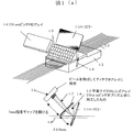
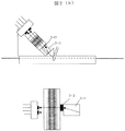
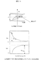
本参考例のインライン型光スペクトルアナライザの基本構造を図1(a)〜図1(c)に示す。
図1(a)において、1−1はハーフミラー、1−2はファイバアレイを固定するV溝アレイ、1−3はテープファイバ、1−4は斜めに形成された30〜40μm幅の溝であり、ここでは溝(1−4)の角度は、テープファイバ(1−3)の延長方向に垂直な直線に対して、22.5度とされる。
1−5は、平面マイクロレンズアレイを45度の頂角を持つプリズム状に加工したプリズムマイクロレンズアレイ、1−6はディテクタアレイ、1−7はファイバからの信号光をハーフミラーで反射された光をマイクロレンズアレイでコリメートしたビームアレイ、1−8はファイバコア、1−9はプリズム面に形成されたARコートである。
Hereinafter, embodiments of the present invention will be described in detail with reference to the drawings.
In all the drawings for explaining the embodiments, parts having the same functions are given the same reference numerals, and repeated explanation thereof is omitted.
[ Reference Example 1 ]
An optical spectrum analyzer will be described as Reference Example 1 of the present invention.
The basic structure of the inline-type optical spectrum analyzer of this reference example is shown in FIGS. 1 (a) to 1 (c).
In FIG. 1 (a), 1-1 is a half mirror, 1-2 is a V-groove array for fixing the fiber array, 1-3 is a tape fiber, and 1-4 is a 30-40 μm wide groove formed obliquely. In this case, the angle of the groove (1-4) is 22.5 degrees with respect to a straight line perpendicular to the extending direction of the tape fiber (1-3).
1-5 is a prism microlens array obtained by processing a planar microlens array into a prism shape having an apex angle of 45 degrees, 1-6 is a detector array, and 1-7 is a signal reflected from a fiber by a half mirror. A beam array obtained by collimating light with a microlens array, 1-8 is a fiber core, and 1-9 is an AR coat formed on a prism surface.
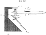
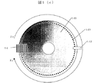
図1(b)、(c)において、1−10はディスクフィルタであり、ディスクフィルタ(1−10)は、円周方向に透過波長が変化している。
1−11はファイバアレイとディテクタアレイを固定するジグ、1−12はディスクフィルタの位置をモニタするセンサ部、1−13は円周上に設けたマーカであり、このマーカ(1−13)の数をカウントすることにより、その透過スペクトル波長を決定する。
本参考例では、プリズムマイクロレンズアレイ(1−5)として、イオン拡散によってガラス表面に屈折率分布を持たせてレンズとした平面マイクロレンズアレイを例に挙げて説明しているが、通常の凸形のレンズアレイでも構わない。
溝の角度は22.5度を代表とし、出射角度は45度が望ましいが、溝(1−4)の角度は、0度以上90度以下であれば、反射光は上に取り出すことができる。
In FIGS. 1B and 1C, reference numeral 1-10 denotes a disk filter, and the transmission wavelength of the disk filter (1-10) changes in the circumferential direction.
1-11 is a jig for fixing the fiber array and the detector array, 1-12 is a sensor unit for monitoring the position of the disk filter, and 1-13 is a marker provided on the circumference of the marker (1-13). The transmission spectrum wavelength is determined by counting the number.
In this reference example , as the prism microlens array (1-5), a planar microlens array having a refractive index distribution on the glass surface by ion diffusion and used as a lens is described as an example. A shaped lens array may be used.
The groove angle is typically 22.5 degrees and the exit angle is preferably 45 degrees. However, if the angle of the groove (1-4) is not less than 0 degrees and not more than 90 degrees, the reflected light can be extracted upward. .
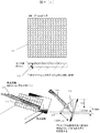
平面マイクロレンズアレイをプリズム状に加工する方法を図3に示す。
マイクロレンズアレイは種々開発されている。ガラス表面、プラスチック表面を凸あるいは凹状に加工したものが代表的である。
このマイクロレンズアレイをプリズム状に加工してもよいが、凹凸があるため、加工が比較的難しい。そこで、屈折率分布をもった平面マイクロレンズを用いるのが最もよい。
平面マイクロレンズは、日本板硝子が開発したレンズアレイであり、代表的には250μmピッチで焦点距離は約0.65mmであり、石英硝子にマスクを塗って、屈折率が高くなるイオン中に浸してイオンを拡散させることによって作製される。
拡散させると表面が凸状になるが、研磨して平坦化している。液晶ディスプレイや通信用レンズとして広く使われている。
この平面マイクロレンズを図3(a)に示すように、表面のレンズ面を底辺とするように、プリズム状に加工する。
図3(a)において、3−1は平面マイクロレンズアレイ基板(通常250μmピッチで配列)、3−2はレンズ面を底辺に持つようにプリズム状に切断研磨したプリズムマイクロレンズアレイ、3−3はファイバ、3−4はハーフミラー、3−5はプリズム形マイクロレンズアレイでコリメートされたビームアレイである。
A method of processing a planar microlens array into a prism shape is shown in FIG.
Various microlens arrays have been developed. A typical example is a glass or plastic surface processed into a convex or concave shape.
The microlens array may be processed into a prism shape, but processing is relatively difficult due to the unevenness. Therefore, it is best to use a planar microlens having a refractive index distribution.
A planar microlens is a lens array developed by Nippon Sheet Glass. Typically, the focal length is about 0.65 mm at a pitch of 250 μm. A quartz glass is coated with a mask and immersed in ions with a high refractive index. It is made by diffusing ions.
When diffused, the surface becomes convex, but is polished and flattened. Widely used as a liquid crystal display and communication lens.
As shown in FIG. 3A, this planar microlens is processed into a prism shape so that the surface lens surface is the base.
3A, reference numeral 3-1 denotes a planar microlens array substrate (usually arranged at a pitch of 250 μm), and 3-2 denotes a prism microlens array that is cut and polished into a prism shape with the lens surface at the bottom. Is a fiber, 3-4 is a half mirror, and 3-5 is a beam array collimated by a prism-shaped microlens array.
ガラス厚は約1mmであるので、ダイシングソーによって45度で切断し、研磨することによって平面マイクロレンズアレイを底辺に持つプリズムマイクロレンズアレイ(3−2)が得られる。
このプリズムマイクロレンズアレイ(3−2)の頂点から底辺までの距離を0.8mm程度として、ファイバ(3−3)(あるいは、導波路)に22.5°に形成した溝にハーフミラー(3−4)を挿入して光を反射させた上に、プリズムマイクロレンズアレイ(3−2)を屈折率が一致した接着剤で固定すると、反射点がちょうど平面マイクロレンズアレイの焦点(ガラス中では焦点距離は0.65mm×1.45=0.94mm)になり、光はコリメートされる。
ファイバの外直径が125μmとすると、45°プリズムの場合、一辺の長さは1.27mmに設定すると焦点距離の所にファイバとミラーの反射点が来る。
平面マイクロレンズアレイは250μmピッチが標準であり、さらにはファイバアレイのピッチも250μmが標準であるので、250μmピッチのビームアレイを45°方向に出射できる。
通常、テープファイバ(3−3)のアレイ数は4、8、12、16、32とあるが、平面マイクロレンズ(3−1)のアレイ数はそれ以上に対応できている。
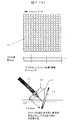
また、図3(b)に示すように、平面マイクロレンズアレイ(3−1)を100μmから200μm程度に薄く研磨し、市販のプリズム(3−7)に張り付けてもよい。
図3(b)において、3−6は薄く研磨された平面マイクロレンズアレイ、3−7はプリズムである。図3(b)に示す方法では、市販のプリズムを適用できるメリットがある。
Since the glass thickness is about 1 mm, a prism microlens array (3-2) having a planar microlens array at the bottom is obtained by cutting at 45 degrees with a dicing saw and polishing.
The distance from the apex to the bottom of the prism microlens array (3-2) is about 0.8 mm, and a half mirror (3) is formed in a groove formed at 22.5 ° in the fiber (3-3) (or waveguide). -4) is inserted to reflect the light, and when the prism microlens array (3-2) is fixed with an adhesive having the same refractive index, the reflection point is exactly the focal point of the planar microlens array (in glass) The focal length is 0.65 mm × 1.45 = 0.94 mm) and the light is collimated.
If the outer diameter of the fiber is 125 μm, in the case of a 45 ° prism, if the length of one side is set to 1.27 mm, the reflection point of the fiber and mirror comes at the focal length.
The planar microlens array has a standard pitch of 250 μm, and the fiber array has a standard pitch of 250 μm. Therefore, a beam array with a pitch of 250 μm can be emitted in the 45 ° direction.
Usually, the number of arrays of tape fibers (3-3) is 4, 8, 12, 16, and 32, but the number of arrays of planar microlenses (3-1) can be more than that.
Further, as shown in FIG. 3B, the planar microlens array (3-1) may be thinly polished to about 100 μm to 200 μm and attached to a commercially available prism (3-7).
In FIG. 3B, 3-6 is a thinly polished planar microlens array, and 3-7 is a prism. The method shown in FIG. 3B has an advantage that a commercially available prism can be applied.
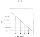
誘電体多層膜フィルタの中で、その位置によって透過波長が変化する波長フィルタがあり、直線方向に線形に波長が変化するタイプと、円盤の円周方向に波長が変化するタイプ(参考文献、鈴木、阿部、橋本、片桐「ディスク形波長可変光フィルタを用いた絶対波長制御法の提案と検証」2002年電子情報通信学会総合大会C−3−79、p.211)がある。
後者では、半値幅の限界は0.1nmで可変波長範囲は150nm程度であり、消光比は40dB以上、ロスは1dB程度である。
ここでは、図1に示すように、後者のフィルタ(本明細書では、ディスクフィルタという)を用いた場合について説明する。
250μmピッチのファイバアレイ(1−3)をV溝に固定して、ハーフミラー(1−1)で反射させて、プリズムマイクロレンズアレイ(1−5)でコリメートビームアレイを形成し、ディスクフィルタ(1−10)を通過させて、ディテクタアレイ(1−6)に入射させる。
ディスクフィルタ(1−10)の外周には破線のマーカ(1−13)が形成されており、このマーカ(1−13)に光を透過させることにより、ディスクフィルタ(1−10)を通過しているビームの光の波長の絶対値を読むことが可能である。
入射側のファイバは、ディスクフィルタ直近に来るため、図1(b)に示すように、ディスクフィルタ(1−10)に接触しないように若干曲げている。
本ディスクフィルタ(1−10)を毎秒1000回転で回転させると、1msで150nmの操引を分解能0.lnmで行い、ディテクタアレイ(1−6)からの出力をADコンバータで1MHz以上の速度で取り込むことにより、多チャンネルのインライン型の光スペクトラムアナライザを実現できる。
波長スイッチ、レベルイコライザなどにおいて、各波長のチャンネルの波長の絶対値、ピークパワーなどを常にモニタして、異常があった場合、パソコンからエラーを出すようにプログラムを組むことが可能となる。
Among dielectric multilayer filters, there are wavelength filters that change the transmission wavelength depending on their position, a type in which the wavelength changes linearly in the linear direction, and a type in which the wavelength changes in the circumferential direction of the disk (references, Suzuki Abe, Hashimoto, Katagiri, “Proposal and Verification of Absolute Wavelength Control Method Using Disk-Type Wavelength Tunable Optical Filter”, 2002 IEICE General Conference C-3-79, p. 211).
In the latter, the limit of the half width is 0.1 nm, the variable wavelength range is about 150 nm, the extinction ratio is 40 dB or more, and the loss is about 1 dB.
Here, as shown in FIG. 1, a case where the latter filter (referred to as a disk filter in this specification) is used will be described.
A fiber array (1-3) having a pitch of 250 μm is fixed to a V groove, reflected by a half mirror (1-1), a collimated beam array is formed by a prism microlens array (1-5), and a disk filter ( 1-10) is allowed to pass through and is incident on the detector array (1-6).
A broken line marker (1-13) is formed on the outer periphery of the disk filter (1-10), and light is transmitted through the marker (1-13) to pass through the disk filter (1-10). It is possible to read the absolute value of the wavelength of the light beam.
Since the incident side fiber comes close to the disk filter, it is bent slightly so as not to contact the disk filter (1-10) as shown in FIG.
When this disk filter (1-10) is rotated at 1000 revolutions per second, an operation of 150 nm can be performed at a resolution of 0.1 in 1 ms. A multi-channel in-line type optical spectrum analyzer can be realized by performing the measurement at 1 nm and capturing the output from the detector array (1-6) at a speed of 1 MHz or more with an AD converter.
In a wavelength switch, level equalizer, etc., it is possible to always monitor the absolute value of the wavelength of each channel, the peak power, etc., and if there is an abnormality, a program can be set up to issue an error from the personal computer.
次に、液晶可変波長フィルタを用いる場合について説明する。
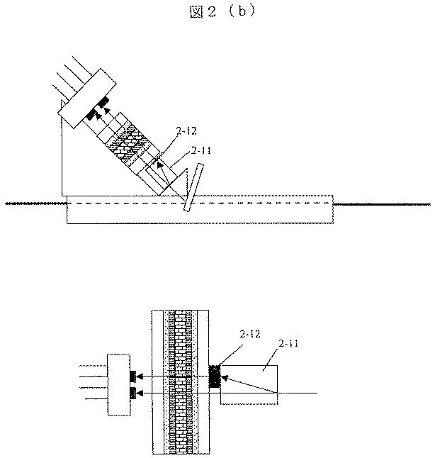
ディスクフィルタ(1−10)は、機械回転式であるので信頼性が落ちるという欠点がある。そこでメカニカル部分のない、液晶可変波長光フィルタを用いてインライン型スペクトラムアナライザを構成する構造を、図2(a)、(b)、(c)に示す。
図2(a)は、λ/4板(2−7)とミラー(2−6)を用いて偏波依存性を解消するタイプの液晶可変波長フィルタを示す図、図2(b)は、偏光分離により偏波依存性を解消するタイプの液晶可変波長フィルタを示す図である。
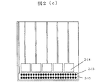
図2(c)は、液晶可変波長フィルタの正面を示す図である。
図2(a)、(b)、(c)において、2−1は2列のディテクタアレイ、2−2は平坦なガラス、2−3は透明電極、2−4は誘電体ミラー、2−5はネマチック液晶、2−6はミラー、2−7はλ/4板、2−8は入射する光ビーム、2−9は三角支持台、2−10は平面マイクロレンズをプリズム状に加工したプリズムマイクロレンズアレイ、2−11は方解石(カルサイト)を代表とする偏光分離素子、2−12はλ/2板、2−13は液晶フィルタを通過する光ビームアレイ、2−14は容量をモニタするための分割された透明電極パターン、2−15は液晶フィルタを駆動するための透明電極パターンである。
Next, a case where a liquid crystal variable wavelength filter is used will be described.
Since the disk filter (1-10) is a mechanical rotary type, there is a drawback that reliability is lowered. Therefore, FIGS. 2A, 2B, and 2C show a structure in which an in-line type spectrum analyzer is configured using a liquid crystal variable wavelength optical filter without a mechanical portion.
FIG. 2A is a diagram showing a liquid crystal tunable wavelength filter that eliminates polarization dependence using a λ / 4 plate (2-7) and a mirror (2-6), and FIG. It is a figure which shows the liquid crystal variable wavelength filter of the type which eliminates polarization dependence by polarization separation.
FIG. 2C is a diagram showing the front of the liquid crystal variable wavelength filter.
2A, 2B and 2C, reference numeral 2-1 denotes a two-row detector array, 2-2 a flat glass, 2-3 a transparent electrode, 2-4 a dielectric mirror, 2- 5 is a nematic liquid crystal, 2-6 is a mirror, 2-7 is a λ / 4 plate, 2-8 is an incident light beam, 2-9 is a triangular support base, and 2-10 is a planar microlens processed into a prism shape. Prism microlens array, 2-11 is a polarization separation element represented by calcite (calcite), 2-12 is a λ / 2 plate, 2-13 is a light beam array passing through a liquid crystal filter, and 2-14 is a capacitance. A divided transparent electrode pattern 2-15 for monitoring is a transparent electrode pattern for driving the liquid crystal filter.
液晶可変波長フィルタは偏波依存性があるため、偏波無依存化する必要がある。
但し、ディテクタで直接受けるため、偏光分離した2本のビームを再度1本のビームに戻す必要はなく、2列のディテクタアレイ(2−1)に分離した2列の光ビームアレイをディテクタアレイ(2−1)に入射させればよい。
偏光分離の方法は、図2(b)に示すように、偏光分離素子(カルサイトあるいは偏光ビームスプリッタ+プリズム)(2−11)によって、2本のp、s偏波に分離し、片方のビームをλ/2板(2−12)で90°回転させて、2本とも液晶の配向と同じ偏光方向にして液晶可変波長フィルタを通過させる方法と、図2(a)に示すように、液晶可変波長フィルタの入射側にλ/4板(2−7)とミラー(2−6)を張り付け、入射した光の内、透過された光以外の波長を反射させこれをλ/4板(2−7)とミラー(2−6)によって再度液晶可変波長フィルタに入射させる方法がある。
液晶可変波長フィルタは、配向膜/誘電体ミラー(2−4)/透明電極(2−3)/ガラス基板(2−2)でネマチック液晶(2−5)を挟んだ液晶エタロンの構造を持ち、誘電体ミラー(2−4)の平行度を高精度に調整したものであり、数V電圧を印加するだけで波長は150nm以上変化する。フィネスは150程度であるので、分解能は1nmとディスクフィルタに比べると低い。
Since the liquid crystal variable wavelength filter has polarization dependence, it is necessary to make the polarization independent.
However, since it is directly received by the detector, there is no need to return the two beams separated by polarization to one beam again, and the two rows of light beam arrays separated into the two rows of detector arrays (2-1) are detected as detector arrays ( 2-1).
As shown in FIG. 2B, the polarization separation method is performed by separating the light into two p and s polarized waves by a polarization separation element (calcite or polarization beam splitter + prism) (2-11). A method in which the beam is rotated by 90 ° with a λ / 2 plate (2-12) so that both of them pass through the liquid crystal variable wavelength filter with the same polarization direction as the alignment of the liquid crystal, as shown in FIG. A λ / 4 plate (2-7) and a mirror (2-6) are attached to the incident side of the liquid crystal variable wavelength filter, and reflected light other than the transmitted light is reflected in the λ / 4 plate ( 2-7) and a mirror (2-6) to make it enter the liquid crystal variable wavelength filter again.
The liquid crystal variable wavelength filter has a liquid crystal etalon structure in which nematic liquid crystal (2-5) is sandwiched between alignment film / dielectric mirror (2-4) / transparent electrode (2-3) / glass substrate (2-2). The parallelism of the dielectric mirror (2-4) is adjusted with high accuracy, and the wavelength changes by 150 nm or more just by applying a few V voltage. Since the finesse is about 150, the resolution is 1 nm, which is lower than that of the disk filter.
面型の可変波長フィルタとして動作するので、コリメータビームアレイを液晶フィルタに通過させて、ディテクタアレイにカップリングさせる。
ディテクタアレイ(2−1)は2列のアレイであり、2本に分離した1対の光ビームが入射する。電気に変換された後、2つの電気出力をパソコン上で足し算することによって偏波無依存化することが可能である。
前述のディスクフィルタ(1−10)と同様にスペクトラムアナライザアレイを実現できる。
しかし、液晶可変波長フィルタは面内で少し波長分布を持ち、また温度によって透過波長が変化する。
このため、図2(c)に示すように、光が通過する近傍に数カ所ITOをパターニングすることにより、透明電極パターン(2−14)を形成して、□のコンデンサを作り、コンデンサの容量を常にモニタすることにより、温度、外部応力等によってギャップや屈折率が変化しても、常にその位置の正確な波長をモニタして、光スペクトラムアナライザを実現できる(特願平7−147472号「液晶可変波長フィルタの駆動電源装置」参考)。
2本のビームは偏光分離の場合と同様に2列のディテクタアレイ(2−1)に入射させることによって、偏波無依存のインライン形のスペクトラムアナライザを実現できる。
このように、本参考例では、ファイバアレイ、導波路アレイ内の光信号のスペクトルをアレイで測定することができる。
Since it operates as a planar variable wavelength filter, the collimator beam array is passed through the liquid crystal filter and coupled to the detector array.
The detector array (2-1) is a two-row array, and a pair of separated light beams are incident thereon. After being converted to electricity, it is possible to make the polarization independent by adding the two electrical outputs on a personal computer.
A spectrum analyzer array can be realized in the same manner as the disk filter (1-10) described above.
However, the liquid crystal variable wavelength filter has a slight wavelength distribution in the surface, and the transmission wavelength changes depending on the temperature.
Therefore, as shown in FIG. 2 (c), by patterning ITO in the vicinity where light passes, a transparent electrode pattern (2-14) is formed, a capacitor □ is formed, and the capacitance of the capacitor is increased. By constantly monitoring, even if the gap or refractive index changes due to temperature, external stress, etc., it is possible to realize an optical spectrum analyzer by constantly monitoring the exact wavelength at that position (Japanese Patent Application No. 7-147472 “Liquid Crystal”). Refer to “Variable Wavelength Filter Drive Power Supply”).
As in the case of polarization separation, the two beams are incident on the two-row detector array (2-1), thereby realizing an in-line spectrum analyzer independent of polarization.
Thus, in this reference example, the spectrum of the optical signal in the fiber array or waveguide array can be measured by the array.
[実施例1]
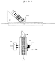
本発明の実施例1として、インライン型偏波状態測定器について説明する。
光の偏光状態を測定するためには、λ/4板あるいはλ/2板、旋光子、直線偏光子を組み合わせ、その通過した4つの出力から偏光状態を知ることができる。
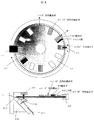
例えば、図4に示すように、円盤の上に0°方向の偏光子、λ/4板+90°方向の偏光子、90°方向の偏光子、および45°方向の偏光子を張り合わせる。
図4において、4−1は直線偏光子、4−2は、45°方向の偏光子、4−3は上側に配置した0°方向の直線偏光子、4−4はλ/4板、4−5は90°方向の直線偏光子、4−6は回転式円盤、4−7は破線マーカである。
4−8は、破線マーカで円盤の回転角度をモニタする部分であり、4−9はディテクタアレイ、4−10は溝に挿入したハーフミラー、4−11はテープファイバであり、テープファイバ(4−11)は、円盤(4−6)に接触しないように、さらに偏波の状態を変化させない程度に曲げられている。4−12はプリズム台、4−13は出射側テープファイバである。
これらの4つの部品を通過した光のパワーを測定することにより、ストークスベクトルを計算できる。この計算方法については後述する。
円盤(4−6)には、1組以上の該偏光子と波長板の組み合わせを張り合わせ、高速で回転させることにより、高速にストークスベクトルを計算できる。
ファイバアレイからの出力を、平面マイクロレンズをプリズム状に加工したプリズムマイクロレンズアレイでコリメートビームアレイにして、円盤(4−6)を回転しながら、ディテクタアレイ(4−9)で出力をモニタして、その出力をADコンバータでパソコンヘ転送することにより、1ms以下の速度で16ch以上のファイバアレイ内の偏波状態を同時に測定できる。
また、円盤上に乗せる波長板、偏光子の組み合わせはこれ以外にも複数あり、種々の組み合わせからストークスベクトルを計算して出力することができる。
[Example 1 ]
As an
In order to measure the polarization state of light, a λ / 4 plate or λ / 2 plate, an optical rotator, and a linear polarizer can be combined, and the polarization state can be known from the four outputs that have passed therethrough.
For example, as shown in FIG. 4, a 0 ° -direction polarizer, a λ / 4 plate + 90 ° -direction polarizer, a 90 ° -direction polarizer, and a 45 ° -direction polarizer are laminated on a disk.
In FIG. 4, 4-1 is a linear polarizer, 4-2 is a 45 ° polarizer, 4-3 is a 0 ° linear polarizer arranged on the upper side, 4-4 is a λ / 4 plate, 4 -5 is a 90 ° linear polarizer, 4-6 is a rotating disk, and 4-7 is a broken line marker.
4-8 is a part for monitoring the rotation angle of the disk with a broken line marker, 4-9 is a detector array, 4-10 is a half mirror inserted in the groove, 4-11 is a tape fiber, and tape fiber (4 -11) is bent so as not to change the state of polarization so as not to contact the disk (4-6). 4-12 is a prism base, and 4-13 is an output side tape fiber.
By measuring the power of the light that has passed through these four parts, the Stokes vector can be calculated. This calculation method will be described later.
A Stokes vector can be calculated at high speed by laminating one or more combinations of the polarizer and the wave plate on the disk (4-6) and rotating the disk at a high speed.
The output from the fiber array is converted into a collimated beam array by a prism microlens array obtained by processing a planar microlens into a prism shape, and the output is monitored by the detector array (4-9) while rotating the disk (4-6). By transferring the output to the personal computer with an AD converter, the polarization state in the fiber array of 16 channels or more can be measured simultaneously at a speed of 1 ms or less.
In addition, there are a plurality of combinations of wave plates and polarizers placed on the disk, and Stokes vectors can be calculated and output from various combinations.
[実施例2]
本発明の実施例2として、インライン型直線偏波モニタについて説明する。
インライン型の直線偏波モニタは、その前段に、偏波制御素子アレイを付けて、(1)ファイバアレイ内の偏波を常に直線偏波に変換するためのモニタとして用いたり、(2)偏波モード分散制御において直線偏光子を通過した高速に変調された光信号の高次モードの電気RFパワーをモニタしてそのパワーを最大にするように制御することにより、偏波モード分散制御する(参考文献:M.Hayashi,H.Tanaka,and M.Suzuki,"40Gb/s demonstration of wide range PMD-compensation using a polarizer" OECC2001,48-49,2001)ために用いられる。
従来、1本でコリメータとして、その間に偏光ビームスプリッタを付けることによって、直線偏波成分をモニタしていたが、多チャンネルのコリメータがないため多チャンネル化ができなかった。
本発明では多チャンネル化が可能である。固定の偏光子をディテクタの前に配置する際、コリメートレンズを付けた場合と付けない場合について説明する。
[Example 2 ]
As an
An in-line type linearly polarized wave monitor is equipped with a polarization control element array in the preceding stage, and (1) it can be used as a monitor for always converting the polarization in the fiber array into a linearly polarized wave. In the wave mode dispersion control, the polarization mode dispersion control is performed by monitoring the electric RF power of the higher-order mode of the optical signal modulated at high speed that has passed through the linear polarizer and maximizing the power. Reference: M. Hayashi, H. Tanaka, and M. Suzuki, “40Gb / s demonstration of wide range PMD-compensation using a polarizer” (OECC 2001, 48-49, 2001).
Conventionally, a single polarization collimator was used as a collimator to monitor a linearly polarized wave component between them. However, since there was no multi-channel collimator, it was not possible to increase the number of channels.
In the present invention, the number of channels can be increased. A case where a collimator lens is attached and a case where a fixed polarizer is placed in front of the detector will be described.
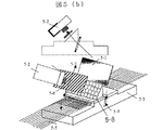
固定型偏光子を用いて偏波を安定化させた場合
図5(a)に示すように、ハーフミラーから反射された光をコリメートレンズを付けずに偏光子を通してディテクタアレイで受けてもよい。
図5(a)において、5−1はハーフミラー、5−2はディテクタアレイ、5−3はV溝アレイを形成したガラス基板、5−4は斜めに形成した溝、5−5はテープファイバ、5−6は直線偏光子であり、5−7は直線偏光子の偏光軸の方向を示す。
一般に、偏光子は、通常その面に垂直に光を通過させた場合に最も消光比が高くなるように設計されている。
図5(a)のように、光ビームが偏光子に対して約45°の角度で入射すると消光比は低下する。ポーラコア(コーニング製直線偏光子)を用いた場合には、長波長側の特性が低下する。200μm厚の偏光子ポーラコアは本来60dB程度の消光比を持つが45°傾けているため、長波長側で消光比が20dB程度と低下する。
ここでは、偏光子の偏光軸をファイバと平行に配置しているが、直交させて配置するとさらに消光比は低下してしまう。
1550nm以下であれば消光比は18dB程度得られるため、コリメートレンズを挿入する必要はないが、図5(b)に示すように、平面マイクロレンズをプリズム状に加工したプリズムマイクロレンズアレイ(5−8)を配置して、45°方向に光を反射させて光が垂直に入射するように直線偏光子(5−6)とディテクタアレイ(5−2)を配置することにより、消光比を劣化させることなく、直線偏波成分をファイバを通過する光に何ら影響を及ぼすことなくモニタすることが可能となり、(1)偏波安定化、(2)偏波モード分散制御のアレイ化に非常に有効である。
When Polarization is Stabilized Using a Fixed Polarizer As shown in FIG. 5A, light reflected from a half mirror may be received by a detector array through a polarizer without a collimating lens.
In FIG. 5A, 5-1 is a half mirror, 5-2 is a detector array, 3-3 is a glass substrate on which a V-groove array is formed, 5-4 is an oblique groove, and 5-5 is a tape fiber. , 5-6 are linear polarizers, and 5-7 indicates the direction of the polarization axis of the linear polarizer.
In general, a polarizer is usually designed to have the highest extinction ratio when light is passed perpendicularly to its surface.
As shown in FIG. 5A, when the light beam is incident on the polarizer at an angle of about 45 °, the extinction ratio decreases. When a polar core (Corning linear polarizer) is used, the characteristics on the long wavelength side deteriorate. The polarizer polar core having a thickness of 200 μm originally has an extinction ratio of about 60 dB, but is inclined 45 °, so that the extinction ratio decreases to about 20 dB on the long wavelength side.
Here, the polarization axis of the polarizer is arranged in parallel to the fiber, but the extinction ratio is further reduced if it is arranged orthogonally.
If it is 1550 nm or less, an extinction ratio of about 18 dB can be obtained, so there is no need to insert a collimating lens. However, as shown in FIG. 5B, a prism microlens array (5- 8) and the extinction ratio is deteriorated by arranging the linear polarizer (5-6) and the detector array (5-2) so that the light is incident vertically by reflecting light in the 45 ° direction. Therefore, it is possible to monitor the linearly polarized wave component without affecting the light passing through the fiber, and (1) polarization stabilization, and (2) polarization mode dispersion control array. It is valid.
回転型偏光子を用いて、任意の方向の直線偏波の成分をモニタする場合
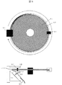
先の例では、直線偏光子(5−6)の向きは決まっていたため、決まった方向の直線偏波成分しかモニタできなかった。
本例では、前述の参考例1で示したように、円盤型に直線偏光子を加工し、平面マイクロレンズをプリズム状に加工したプリズムマイクロレンズアレイとディテクタアレイの間に配置し、円盤状の偏光子を回転させることにより、その直線偏光子の方向を任意に変えることにより、任意の方向の直線偏波の成分をアレイでモニタすることが可能となる。図6にその構造を示す。
図6において、6−1は円盤状に加工した直線偏光子、6−2はその周図に付けた偏光子の軸の方向をモニタするためのマーカ、6−3はディテクタアレイ、6−4はマーカモニタ、6−5はファイバアレイを固定したV溝ガラス基板、6−6は溝に挿入したハーフミラー、6−7は平面マイクロレンズをプリズム状に加工したプリズムマイクロレンズアレイ、6−8はファイバアレイから反射されてコリメートされた光ビームアレイ、6−9はこれらの部品を支持する固定ジグである。
直線偏光子(6−1)を回転させ、マーカ(6−2)の数をカウントすることにより、その直線偏光子(6−1)の角度を読みとり、その角度の直線偏光成分をディテクタアレイ(6−3)でモニタすることが可能となる。
このため、任意の角度の直線偏波を得るために、このインライン形のディテクタアレイを用いると、その強度を最大あるいは最小にすることにより、所望の方向の直線偏波に制御することが可能となる。
When using a rotating polarizer to monitor the component of linearly polarized light in an arbitrary direction In the previous example, the direction of the linear polarizer (5-6) has been determined, so only the linearly polarized component in the determined direction can be detected. Could not monitor.
In this example, as shown in the above-mentioned Reference Example 1, a linear polarizer is processed into a disk shape, and a planar microlens is arranged between a prism microlens array and a detector array that are processed into a prism shape. By rotating the polarizer to arbitrarily change the direction of the linear polarizer, it is possible to monitor the linearly polarized component in an arbitrary direction with the array. FIG. 6 shows the structure.
In FIG. 6, 6-1 is a linear polarizer processed into a disk shape, 6-2 is a marker for monitoring the direction of the axis of the polarizer attached to the circumference, 6-3 is a detector array, 6-4 Is a marker monitor, 6-5 is a V-groove glass substrate to which a fiber array is fixed, 6-6 is a half mirror inserted into the groove, 6-7 is a prism microlens array obtained by processing a planar microlens into a prism shape, and 6-8. Is a collimated light beam array reflected from the fiber array, and 6-9 is a fixed jig for supporting these components.
By rotating the linear polarizer (6-1) and counting the number of markers (6-2), the angle of the linear polarizer (6-1) is read, and the linearly polarized light component of the angle is detected by the detector array ( 6-3) can be monitored.
For this reason, in order to obtain a linearly polarized wave of an arbitrary angle, this in-line detector array can be controlled to a linearly polarized wave in a desired direction by maximizing or minimizing its intensity. Become.
[実施例3]
本発明の実施例3として、ハーフミラーの反射率の偏波依存性を解消する方法を説明する。
ストークスベクトルを正確に求める場合、ハーフミラー(図1の1−1)で反射された光の偏波および通過する光の偏波は同じであり、また位相差が生じないようにする必要がある。このため、ハーフミラーを構成する誘電体ミラーの層構成を最適設計する必要がある。
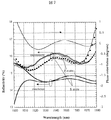
ハーフミラーの角度、反射率を設定して、誘電体ミラーの高屈折率層と低屈折率層の膜厚を振って、ある波長領域でp、s偏波に対する反射率を計算し、その偏波依存性が最低になるようにシミュレーションする。その結果、最低20層以上の膜を形成することにより、計算および実験結果からほぼ偏波依存性のない反射率を得られることがわかった。
Ta2O5/SiO2多層膜とし、それらの厚さをλ/4からλ/2近くの厚さにして、その層数を25層として、反射率の計算値と実測値および位相差の計算値の結果を図7に示す。
本実施例の誘電体ミラーでは、溝の角度が22.5°で反射率が15%になり、位相差が最低になり、p、s偏波の反射率が15%になるように設計した。
層の総数は25層であり、約6μmの厚さがある。実際の測定値も図7に示す。このようにミラーの層厚を20層以上とし、それぞれの膜厚を調整することによって、反射率のp、s偏波依存性がなく、位相差が生じない誘電体ミラーを形成できる。
[Example 3 ]
As a third embodiment of the present invention, a method for eliminating the polarization dependency of the reflectance of the half mirror will be described.
When accurately obtaining the Stokes vector, the polarization of the light reflected by the half mirror (1-1 in FIG. 1) and the polarization of the passing light must be the same, and it is necessary to prevent a phase difference from occurring. . Therefore, it is necessary to optimally design the layer configuration of the dielectric mirror that constitutes the half mirror.
The angle and reflectance of the half mirror are set, the film thicknesses of the high refractive index layer and low refractive index layer of the dielectric mirror are varied, and the reflectance for p and s polarized waves is calculated in a certain wavelength region. Simulate to minimize wave dependency. As a result, it was found that a reflectance having almost no polarization dependence can be obtained from calculation and experimental results by forming a film of at least 20 layers.
The Ta 2 O 5 / SiO 2 multilayer films are made to have a thickness between λ / 4 and λ / 2, and the number of layers is 25. The result of the calculated value is shown in FIG.
The dielectric mirror of this example was designed so that the groove angle was 22.5 ° and the reflectivity was 15%, the phase difference was minimized, and the reflectivity of p and s polarized waves was 15%. .
The total number of layers is 25 and has a thickness of about 6 μm. Actual measured values are also shown in FIG. In this way, by setting the mirror layer thickness to 20 layers or more and adjusting the respective film thicknesses, it is possible to form a dielectric mirror that does not depend on the p and s polarization of the reflectance and does not cause a phase difference.
[実施例4]
本発明の実施例4として、誘電体ミラーの層構成、溝へ挿入固定の接着剤の屈折率マッチィングについて説明する。
誘電体ミラー(図1の1−1)を、Ta2O5/SiO2多層膜とし、それらの厚さをλ/4からλ/2近くの厚さにして、その層数を25層として研磨後、屈折率がファイバの屈折率1.45と一致した接着剤で、溝に挿入して接着した。透過の偏波依存性は0.06dBであり、反射の偏波依存性は0.02dBであった。
これに対して、接着剤が1.5の物を用いると、透過の偏波依存性は0.2dB、反射の偏波依存性も0.5dB以上と大きくなった。このため、偏波依存性がなく、位相差が生じない誘電体ミラーは、層の数は20層以上で、溝に挿入−固定する際の接着剤はファイバ−導波路の屈折率に一致していることが必要となる。
[Example 4 ]
As Example 4 of the present invention, the layer configuration of a dielectric mirror and the refractive index matching of an adhesive that is inserted and fixed in a groove will be described.
The dielectric mirror (1-1 in FIG. 1) is a Ta 2 O 5 / SiO 2 multilayer film, the thickness thereof is changed from λ / 4 to near λ / 2, and the number of layers is 25. After polishing, the adhesive was inserted into the groove and adhered with an adhesive whose refractive index matched the refractive index of 1.45 of the fiber. The polarization dependency of transmission was 0.06 dB, and the polarization dependency of reflection was 0.02 dB.
On the other hand, when a material having an adhesive of 1.5 was used, the polarization dependency of transmission was as large as 0.2 dB, and the polarization dependency of reflection was as large as 0.5 dB or more. For this reason, a dielectric mirror that does not depend on polarization and does not cause a phase difference has 20 or more layers, and the adhesive used when inserting and fixing in the groove matches the refractive index of the fiber-waveguide. It is necessary to be.
[参考例2]
本発明の参考例2として、回折格子を持つ光スペクトラムアナライザについて説明する。
先の実施例では、円盤形可変波長フィルタ、液晶可変波長フィルタを用いたが、回折格子(グレーティング)でも同様に光スペクトルを測定することができる。図8にその構造を示す。
図8において、8−1はグレーティング、8−2はレンズ、8−3は2次元ディテクタアレイ、8−4はプリズムレンズアレイ、8−5はハーフミラー、8−6はテープファイバ、8−7は分光した光である。
ハーフミラー(8−5)で反射した光はグレーティング(8−1)によって回折されて、分光され、2次元のディテクタアレイ(8−3)に入射し、ディテクタアレイ(8−3)で光スペクトルを測定できる。
なお、図8では、固定のグレーティングを記載しているが、回転形グレーティングを用いると、1次元のディテクタアレイを配置することにより、光スペクトラムアナライザアレイを実現することができる。
[ Reference Example 2 ]
An optical spectrum analyzer having a diffraction grating will be described as Reference Example 2 of the present invention.
In the previous embodiment, the disk-shaped variable wavelength filter and the liquid crystal variable wavelength filter are used. However, the optical spectrum can be similarly measured using a diffraction grating (grating). FIG. 8 shows the structure.
In FIG. 8, 8-1 is a grating, 8-2 is a lens, 8-3 is a two-dimensional detector array, 8-4 is a prism lens array, 8-5 is a half mirror, 8-6 is a tape fiber, 8-7. Is spectroscopic light.
The light reflected by the half mirror (8-5) is diffracted by the grating (8-1), dispersed, and incident on the two-dimensional detector array (8-3), and the optical spectrum by the detector array (8-3). Can be measured.
In FIG. 8, a fixed grating is shown. However, if a rotating grating is used, an optical spectrum analyzer array can be realized by arranging a one-dimensional detector array.
[実施例5]
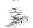
本発明の実施例5として、先の実施例2で作製したインライン形固定偏光子付きディテクタアレイを用いて、ファイバアレイ内の偏波を常にTE偏波に変換して、光導波路に入力する系を図9に示す。
図9では、液晶偏波制御素子により、ファイバアレイ内の偏波を制御している。(特願2002−068880号「導波路型光素子及びその作製方法」参照)
図9において、9−1は光導波路の光導入部であり、9−2は実施例2で作製したインライン形偏光子付きディテクタアレイである。
9−3はファイバアレイに固定したファイバアレイに2本の溝を形成して薄い液晶偏波制御素子を挿入した偏波制御回路であり、インライン形偏光子付きディテクタアレイ(9−2)の直線偏光子を通過した光のパワーを最小にするようにフィードバックをかけることにより、常に導波路に入力する偏波がTE偏波になる。
導波路自体は大きな複屈折を持つため、TE偏波が入力されるとTE偏波のままで導波路内を伝搬するので、導波路の偏波依存性がなくなるという大きなメリットがある。
[Example 5 ]
As a fifth embodiment of the present invention, a system in which the polarization in the fiber array is always converted to a TE polarization and input to the optical waveguide using the detector array with an inline fixed polarizer produced in the second embodiment. Is shown in FIG.
In FIG. 9, the polarization in the fiber array is controlled by the liquid crystal polarization control element. (See Japanese Patent Application No. 2002-068880 “Waveguide type optical element and method for manufacturing the same”)
In FIG. 9, reference numeral 9-1 denotes a light introducing portion of the optical waveguide, and 9-2 denotes a detector array with an inline-type polarizer manufactured in the second embodiment.
Reference numeral 9-3 denotes a polarization control circuit in which two grooves are formed in a fiber array fixed to the fiber array and a thin liquid crystal polarization control element is inserted, and is a straight line of a detector array (9-2) with an inline polarizer. By applying feedback so as to minimize the power of the light that has passed through the polarizer, the polarization that is always input to the waveguide becomes TE polarization.
Since the waveguide itself has a large birefringence, when TE polarized light is input, it propagates in the waveguide while maintaining the TE polarized wave, which has a great merit that the polarization dependency of the waveguide is eliminated.
[実施例6]
先の実施例1から実施例5、参考例1、参考例2までは、ファイバアレイ・導波路アレイ内の光の偏波状態、スペクトル状態をアレイでモニタするものについて説明した。
これらの光アレイの状態をモニタした後、その結果を持って制御をする必要が出てくる。例えば、偏波状態をモニタした場合には、その結果を基に偏波制御する。フィードフォワード方式において、偏波をモニタした位置での偏波を制御する必要がある。
具体的には、コヒーレント通信におけるフィードフォワード偏波制御、あるいは偏波モード分散補償がこれに当たる。
しかし、偏波状態モニタの後、テープファイバで偏波制御器を接続すると、ファイバが固定されていないため、偏波状態が変化してしまっている。
そこで、本実施例の偏波状態測定器を作製したファイバ基板・導波路の同一基板上に偏波制御器を設置することが必要である。
そのためには、本実施例の偏波測定器、参考例の光スペクトラム測定器を作製した時と同様に、同一基板上のファイバ・導波路アレイに溝を形成して、アクティブ面型素子(例えば、液晶の偏波制御器アレイあるいは薄いPLZT偏波制御器アレイなどの偏波制御器)を挿入すればよい。(参考文献:K.Hirabayashi, and C.Amamo, "Liquid-Crystal Polarization Controller Arrays on Planar Waveguide Circuits," IEEE PTL vol.14,No.4,April p.504-506,2002、K.Hirabayashi,and C.Amano, "Variable and Rotatable Waveplates of PLZT Electro-Optic Ceramic Material on Planar Waveguide Circuits,"IEEE PTL vol.14,No.7,July, p.956-958,2002)
このようにすることにより、偏波をモニタした箇所で直接偏波制御が可能となる。また、スペクトル状態をモニタした場合には、薄型の可変減衰器などのアクティブ面型素子を溝に挿入することにより、選択された波長の強度を制御することができる。
[Example 6 ]
In the first embodiment to the fifth embodiment , the first reference example, and the second reference example , description has been made on the case where the polarization state and the spectral state of light in the fiber array / waveguide array are monitored by the array.
After monitoring the state of these optical arrays, it becomes necessary to perform control with the result. For example, when the polarization state is monitored, the polarization control is performed based on the result. In the feedforward method, it is necessary to control the polarization at the position where the polarization is monitored.
Specifically, this is feedforward polarization control or polarization mode dispersion compensation in coherent communication.
However, when the polarization controller is connected with a tape fiber after monitoring the polarization state, the polarization state has changed because the fiber is not fixed.
Therefore, it is necessary to install a polarization controller on the same substrate of the fiber substrate and the waveguide on which the polarization state measuring device of this embodiment is manufactured.
For this purpose, a groove is formed in the fiber waveguide array on the same substrate as in the case of manufacturing the polarization measuring instrument of this embodiment and the optical spectrum measuring instrument of the reference example , and active surface type elements (for example, A polarization controller such as a liquid crystal polarization controller array or a thin PLZT polarization controller array may be inserted. (Reference: K.Hirabayashi, and C. Amamo, "Liquid-Crystal Polarization Controller Arrays on Planar Waveguide Circuits," IEEE PTL vol.14, No.4, April p.504-506,2002, K.Hirabayashi, and C. Amano, "Variable and Rotatable Waveplates of PLZT Electro-Optic Ceramic Material on Planar Waveguide Circuits," IEEE PTL vol.14, No.7, July, p.956-958, 2002)
In this way, direct polarization control can be performed at a location where polarization is monitored. When the spectral state is monitored, the intensity of the selected wavelength can be controlled by inserting an active surface element such as a thin variable attenuator into the groove.
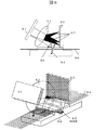
[実施例7]
図10は、本発明の実施例7の偏波状態測定器を示す図であり、同図(a)は正面図、同図(b)は斜視図、同図(c)は偏波測定部のみの外観図、同図(d)は偏波測定部の側面図である。
同図において、11−1は位相制御素子を構成する電気光学セラミクス、11−2は電気光学セラミクス(11−1)を挟む2つの電極、11−3はファイバあるいは導波路を固定する固定板、11−4はファイバあるいは導波路のコア、11−5は固定板(11−3)に形成された溝に挿入される誘電体ミラー、11−6はプリズム、11−7は平面マイクロレンズ、11−8は偏光分離素子、11−9は2個のディテクタ、11−10は電気光学セラミクス(11−1)を乗せる三角形状の台、11−11は入出力ファイバ、11−12は誘電体ミラーで反射された光ビーム、11−13はモニタ光を作るコリメータ付きレーザダイオード、11−14はモニタビーム、11−15はモニタ光用ディテクタ、11−16はモニタ光用の45°の方向を向いた直線偏光子、11−17はモニタ光用の−45°の方向を向いた直線偏光子、11−18は電気光学セラミクス(11−1)に電圧を印加するパルス電源である。
なお、本実施例では、電気光学セラミクス(11−1)として、PLZTを使用している。
また、平面マイクロレンズ(11−7)は、通常のマクロレンズでもよく、さらに、偏光分離素子(11−8)は直交方向に分離するタイプもので、方解石などの異方性光学結晶、あるいは偏光ビームスプリッタが使用される。
また、平面マイクロレンズ(11−7)とプリズム(11−6)に代えて、前述のプリズムマイクロレンズアレイを使用することもできる。
[Example 7 ]
10A and 10B are diagrams showing a polarization state measuring apparatus according to a seventh embodiment of the present invention. FIG. 10A is a front view, FIG. 10B is a perspective view, and FIG. 10C is a polarization measuring unit. FIG. 4D is a side view of the polarization measuring unit.
In the figure, 11-1 is an electro-optic ceramic constituting a phase control element, 11-2 is two electrodes sandwiching the electro-optic ceramic (11-1), 11-3 is a fixing plate for fixing a fiber or a waveguide, 11-4 is a fiber or waveguide core, 11-5 is a dielectric mirror inserted into a groove formed in the fixed plate (11-3), 11-6 is a prism, 11-7 is a planar microlens, 11 -8 is a polarization separation element, 11-9 is two detectors, 11-10 is a triangular base on which the electro-optic ceramic (11-1) is placed, 11-11 is an input / output fiber, and 11-12 is a dielectric mirror. 11-13 is a laser diode with a collimator for producing monitor light, 11-14 is a monitor beam, 11-15 is a detector for monitor light, and 11-16 is 4 for monitor light. Is a linear polarizer oriented in the direction of °, 11-17 is a linear polarizer oriented in the direction of -45 ° for monitor light, and 11-18 is a pulse power source for applying a voltage to the electro-optic ceramic (11-1). is there.
In this embodiment, PLZT is used as the electro-optic ceramic (11-1).
The planar microlens (11-7) may be a normal macrolens, and the polarization separation element (11-8) is of a type that separates in an orthogonal direction, and is an anisotropic optical crystal such as calcite, or polarized light. A beam splitter is used.
Further, the above-described prism microlens array can be used in place of the planar microlens (11-7) and the prism (11-6).
本実施例の偏波状態測定器は、ファイバあるいはファイバアレイあるいは導波路のコア(11−4)を横切るように、固定板(11−3)に形成した溝に誘電体ミラー(ハーフミラー)(11−5)を挿入し、当該誘電体ミラー(11−5)で反射させた光を、コリメートレンズ(11−7)でコリメートし、この光ビームを、2枚の電極(11−2)で挟んだ1枚の電気光学セラミクス(11−1)を通過させる。
また、電気光学セラミクス(11−1)の後段に、p偏波とs偏波の2つに分離する偏光分離素子(11−8)を配置し、p偏波とs偏波の出力を2個のディテクタ(11−9)で検出するようになし、電気光学セラミクス(11−1)に、0Vと1/4波長電圧(位相がπ/2)、半波長電圧(位相がπ)を印加し、そのときの2個のディテクタ(11−9)の出力からストークスパラメータを算出する。
ファイバあるいは導波路の光を外部に取り出す際、誘電体ミラー(11−5)によって偏波が変化しないように、誘電体ミラー(11−5)を挿入する溝の角度は30°以下が望ましく(この角度を、22.5°に設定すると、反射した光は45°の角度になり、プリズムなど、汎用品をそのまま用いることが可能である)、さらに、誘電体ミラー(11−5)における誘電体多層膜の膜構成を最適に設計しておく必要がある。
なお、本実施例において、電気光学セラミクス(11−1)に代えて、ニオブ酸リチウムなどの電気光学結晶や、平行配向の液晶素子を用いても構わない。
PLZTのカー定数は、R=7×10⁻³(μm/V)2で与えられ、その屈折率変化は、下記(1)式で与えられる。
The polarization state measuring instrument of the present embodiment has a dielectric mirror (half mirror) in a groove formed in the fixed plate (11-3) so as to cross the core (11-4) of the fiber, fiber array, or waveguide. 11-5) is inserted, and the light reflected by the dielectric mirror (11-5) is collimated by the collimating lens (11-7), and this light beam is reflected by the two electrodes (11-2). One sandwiched electro-optic ceramic (11-1) is passed.
In addition, a polarization separation element (11-8) that separates the p-polarized light and the s-polarized light into two parts is disposed at the subsequent stage of the electro-optic ceramics (11-1). Detected by individual detectors (11-9), 0V, 1/4 wavelength voltage (phase π / 2) and half wavelength voltage (phase π) are applied to electro-optic ceramics (11-1) Then, the Stokes parameters are calculated from the outputs of the two detectors (11-9) at that time.
When taking out the light of the fiber or the waveguide to the outside, the angle of the groove into which the dielectric mirror (11-5) is inserted is preferably 30 ° or less so that the polarization is not changed by the dielectric mirror (11-5) ( If this angle is set to 22.5 °, the reflected light becomes an angle of 45 °, and a general-purpose product such as a prism can be used as it is.) Further, the dielectric in the dielectric mirror (11-5) It is necessary to optimally design the film configuration of the body multilayer film.
In this embodiment, instead of the electro-optic ceramic (11-1), an electro-optic crystal such as lithium niobate or a parallel-aligned liquid crystal element may be used.
The Kerr constant of PLZT is given by R = 7 × 10 −3 (μm / V) 2 , and the refractive index change is given by the following equation (1).
![]()
ここで、Eは印加される電界である。
通常、PLZT基板は0.5mm厚研磨品が標準であるので、本実施例では、これを長さ10mmに切断し、この基板の両側に電極を蒸着で付け、1.55μmの光信号を光ビーム(ビーム直径200−300μm)として通過させる。
その際、光ビームの位相シフト量が、0、π/4、π/2、πシフトする電圧は、0V、40.9V、58.8V、81.8Vとなる。
高耐圧のオペアンプを用いることによって、電圧を印加するが、電流は流れないので、1個数万円のオペアンプで電源を作製でき、電源の価格が高くなることはない。
さらに、PLZTの長さを20mmにすれば、それぞれの電圧は、これらの半分の値になり、より安価なオペアンプを使用できる。
![]()
Here, E is an applied electric field.
Usually, a 0.5 mm thick polished product is standard for a PLZT substrate. In this embodiment, this is cut to a length of 10 mm, electrodes are attached to both sides of this substrate by vapor deposition, and an optical signal of 1.55 μm is optically transmitted. Pass as a beam (beam diameter 200-300 μm).
At this time, voltages at which the phase shift amount of the light beam is shifted by 0, π / 4, π / 2, and π are 0V, 40.9V, 58.8V, and 81.8V.
Although a voltage is applied by using a high-voltage operational amplifier, but no current flows, a power supply can be manufactured with an operational amplifier of several tens of thousands of yen, and the price of the power supply does not increase.
Furthermore, if the length of PLZT is 20 mm, each voltage becomes half of these values, and a cheaper operational amplifier can be used.
電気光学セラミクス(11−1)、偏光分離素子(11−8)、およびディテクタ(11−9,11−15)からなる偏光測定部の大きさは、PLZT板に、偏光分離素子(11−8)とディテクタ(11−9,11−15)を付けるのみなので、最大でも、20mm×10mm×10mmの大きさで済み、従来に比べて非常に小型化が可能である。
なお、図10では、1本の光ビームしか図示していないが、ファイバあるいは導波路からの反射光をレンズアレイにより、コリメートビームアレイとし、そのピッチを0.25mmから1mmピッチとして、8チャンネル、あるいは16チャンネルのディテクタアレイで受けても、モジュールの大きさはほぼ1チャンネルと同じである。
但し、PLZTは、位相一電圧特性にヒステリシスを持つ場合があるので、電圧を上昇させた場合と下降させた場合で、数Vの差が生じる。
したがって、本実施例のように、正確に位相量を変化させる必要がある場合には、印加電圧は上昇時のみ、あるいは下降時のみの電圧を印加した場合の、ディテクタの出力を読む必要がある。
The size of the polarization measuring unit including the electro-optic ceramic (11-1), the polarization separation element (11-8), and the detector (11-9, 11-15) is the same as that of the polarization separation element (11-8). ) And the detectors (11-9, 11-15), the size is 20 mm × 10 mm × 10 mm at the maximum, and the size can be greatly reduced as compared with the conventional case.
In FIG. 10, only one light beam is shown, but the reflected light from the fiber or waveguide is made into a collimated beam array by a lens array, the pitch is changed from 0.25 mm to 1 mm, and 8 channels. Alternatively, even if a 16-channel detector array is used, the size of the module is almost the same as that of one channel.
However, since PLZT may have hysteresis in the phase-one voltage characteristic, there is a difference of several V between when the voltage is raised and when it is lowered.
Therefore, when it is necessary to change the phase amount accurately as in the present embodiment, it is necessary to read the output of the detector when the applied voltage is applied only when rising or only when falling. .
以下、入射光のストークスベクトル(w、x、y、z)を算出する方法を説明する。
計算を簡単にするために、絶対座標に対して、電気光学セラミクス(ここでは、PLZT)からなる位相制御素子が、任意の方向(本実施例では、固定板の法線方向)に対して22.5°傾いており、偏光分離素子(11−8)の方向が0°と90°であるとする。
本実施例の偏光測定部では、作製上の都合から、電気光学セラミクス(PLZT基板)(11−1)の軸(PLZT基板に印加する電界方向)が、固定板の法線方向と同一方向(固定板の法線方向に対して0°方向)、偏光分離素子(11−8)が、固定板の法線方向に対して22.5°傾いている。
従って、本計算で得られたストークスベクトルは、本来のストークスベクトルに変換するために、固定板の法線方向に対して−22.5度回転座標変換させる必要がある。
入力光のストークスベクトルを(w、x、y、z)とすると、位相Δが0の時の2個のディテクタ(11−9)の出力1、2は下記(2)式の通りとなる。なお、w=√(x2+Y2+z2)である。
[数2]
出力1(Δ=0):−w/2+x/2
出力2(Δ=0):w/2+x/2
・・・・・・・・・・・・・・・・・・・・・ (2)
Hereinafter, a method for calculating the Stokes vector (w, x, y, z) of incident light will be described.
In order to simplify the calculation, a phase control element made of electro-optic ceramics (here, PLZT) is 22 in any direction (in this embodiment, the normal direction of the fixed plate) with respect to absolute coordinates. It is assumed that the direction of the polarization separating element (11-8) is 0 ° and 90 °.
In the polarization measuring unit of the present embodiment, for the sake of manufacturing, the axis of the electro-optic ceramics (PLZT substrate) (11-1) (the direction of the electric field applied to the PLZT substrate) is the same direction as the normal direction of the fixed plate ( The polarization separation element (11-8) is inclined 22.5 ° with respect to the normal direction of the fixed plate.
Therefore, in order to convert the Stokes vector obtained by this calculation into the original Stokes vector, it is necessary to perform the coordinate conversion of −22.5 degrees with respect to the normal direction of the fixed plate.
When the Stokes vector of the input light is (w, x, y, z), the
[Equation 2]
Output 1 (Δ = 0): −w / 2 + x / 2
Output 2 (Δ = 0): w / 2 + x / 2
(2)
位相Δがπの時の2個のディテクタ(11−9)の出力1、2のストークスベクトルは、それぞれ下記(3)式の通りとなる。
[数3]
{(w/2−y/2)、(−w/2+y/2)、0、0}
{(w/2+y/2)、(w/2+y/2)、0、0}
・・・・・・・・・・・・・・・・・・・・・ (3)
従って、位相がπの時の2個のディテクタ(11−9)の出力1、2は、下記(4)式の通りとなる。
[数4]
出力1(Δ=π):−w/2+y/2
出力2(Δ=π):w/2+y/2
・・・・・・・・・・・・・・・・・・・・・ (4)
位相π/2の時の2個のディテクタ(11−9)の出力1、2のストークスベクトルは、それぞれ下記(5)式の通りとなる。
従って、位相がπ/2の時の2個のディテクタ(11−9)の出力1、2は、それぞれ下記(6)式の通りとなる。
The Stokes vectors of the
[Equation 3]
{(W / 2−y / 2), (−w / 2 + y / 2), 0, 0}
{(W / 2 + y / 2), (w / 2 + y / 2), 0, 0}
・ ・ ・ ・ ・ ・ ・ ・ ・ ・ ・ ・ ・ ・ ・ ・ (3)
Therefore, the
[Equation 4]
Output 1 (Δ = π): −w / 2 + y / 2
Output 2 (Δ = π): w / 2 + y / 2
(4)
The Stokes vectors of the
Therefore, the
次に、電気光学セラミクス(11−1)における、光ビームの位相シフト量が、0、π/4、π/2、πとなる印加電圧を求める方法を説明する。
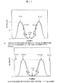
図11(a)に示すように、モニタ光を信号光と同じ波長とすると、クロスニコルの状態で、0Vで光ビームの位相シフト量は0であり、電圧を印加させていくとモニタ光の出力はsin2(Θ)のカーブに乗る。
出力が最大になるように電圧を調整した時の電圧(計算では81.8V)が半波長電圧(位相π)となる。
1/4波長シフトの電圧(π/2)は出力がsin2(Θ)に載ることから、最大値の半分の値になる時の電圧値(計算では58.8V)を求めればよい。
また、モニタ光が、測定する信号光の波長の半分の波長の光、例えば、1.55μmの波長が信号光であれば、780nmのレーザ光をモニタ光とする。780nmのレーザは非常に安価に入手可能である。
信号光が1300nmであれば、さらに安価な赤のレーザポインタ用の650nmの半導体レーザがモニタ光として使用可能である。さらに安価な発光ダイオードを用いてもよい。
この場合には、図11(b)に示すように、出力が最大になる時が1/4波長(π/2)電圧、さらに電圧を上げて出力が最低になるときの電圧が1/2波長電圧(π)となる。
Next, a method for obtaining an applied voltage in which the phase shift amount of the light beam in the electro-optic ceramics (11-1) is 0, π / 4, π / 2, and π will be described.
As shown in FIG. 11A, when the monitor light has the same wavelength as the signal light, the phase shift amount of the light beam is 0 at 0 V in a crossed Nicol state, and when the voltage is applied, the monitor light The output is on a sin 2 (Θ) curve.
A voltage (81.8 V in the calculation) when the voltage is adjusted so as to maximize the output is a half-wave voltage (phase π).
Since the output of ¼ wavelength shift (π / 2) is on sin 2 (Θ), a voltage value (58.8 V in the calculation) at which the output is half the maximum value may be obtained.
Further, if the monitor light is light having a wavelength that is half the wavelength of the signal light to be measured, for example, if the wavelength of 1.55 μm is signal light, then 780 nm laser light is used as the monitor light. 780 nm lasers are available very cheaply.
If the signal light is 1300 nm, a cheaper 650 nm semiconductor laser for a red laser pointer can be used as the monitor light. Further, an inexpensive light emitting diode may be used.
In this case, as shown in FIG. 11B, when the output is maximized, the 1/4 wavelength (π / 2) voltage is obtained, and when the voltage is further increased and the output is minimized, the voltage is 1/2. Wavelength voltage (π).
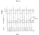
予め、この電圧を手動で求めておき、図12に示すように、0、1/4波長電圧(V(π/2))、1/2波長電圧(V(π))の3つの電圧を繰り返して印加し、そのタイミング時の2個のディテクタ(11−9)の2出力を測定することにより、ほぼリアルタイムで、信号光の偏波状態をモニタすることが可能となる。
PLZTは、応答測度が非常に速く、nsで応答するが、電源やADコンバータの速度が1μs程度であるので、1MHz程度のクロックで測定し、約100kHzで偏波状態を算出できる。
なお、本実施例では、位相制御素子として、電気光学セラミクス(PLZT)を用いたが、位相制御素子としては、ネマチック平行配向液晶を代表とする液晶素子でも、あるいはニオブ酸リチウムを代表とする電気光学結晶を使用してもよい。
液晶素子を用いると、さらに低電圧化できるが、応答測度がms程度であるので、高速な偏波測定はできず、約100Hzでの偏波状態を出力できる。
また、位相制御素子の方向、分離偏光素子の方向は、前述の説明以外に種々の組み合わせがあるが、ここではその1例を示したのみで、本発明は全ての組み合わせを包含する。また光ビームは1本としたが、複数であっても、ディテクタアレイで受けることによって一括で偏波状態を知ることが可能である。
This voltage is obtained manually in advance, and as shown in FIG. 12, three voltages of 0, ¼ wavelength voltage (V (π / 2)), and ½ wavelength voltage (V (π)) are obtained. By repeatedly applying and measuring the two outputs of the two detectors (11-9) at the timing, the polarization state of the signal light can be monitored almost in real time.
PLZT has a very fast response measure and responds in ns. However, since the speed of the power supply and AD converter is about 1 μs, it can be measured with a clock of about 1 MHz and the polarization state can be calculated at about 100 kHz.
In this embodiment, electro-optic ceramics (PLZT) is used as the phase control element. However, as the phase control element, a liquid crystal element typified by nematic parallel alignment liquid crystal or an electric power typified by lithium niobate is used. Optical crystals may be used.
When a liquid crystal element is used, the voltage can be further reduced, but since the response measure is about ms, high-speed polarization measurement cannot be performed, and a polarization state at about 100 Hz can be output.
There are various combinations of the direction of the phase control element and the direction of the separation polarization element in addition to the above description, but only one example is shown here, and the present invention encompasses all combinations. Although the number of light beams is one, even if there are a plurality of light beams, it is possible to know the polarization state at a time by receiving them with the detector array.
[実施例8]
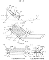
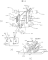
図13は、本発明の実施例8の偏波状態測定器を示す図であり、同図(a)は偏波測定部のみの外観図、同図(b)は偏波測定部の側面図、同図(c)は斜視図である。
同図において、12−1はそれぞれ配向方向が±22.5°の2枚の平行配向液晶素子、12−2は入射光ビーム、12−3は0°方向の直線偏光子、12−4はディテクタ、12−5はモニタ光用の67.5°の方向を向いた直線偏光子、12−6はモニタ光用の−22.5°の方向を向いた直線偏光子、12−7はモニタ用レーザあるいは発光ダイオード、12−8はパルス電源、11−5は固定板(11−3)に形成された溝に挿入される誘電体ミラー、11−6はプリズム、11−7は平面マイクロレンズまたは平面マイクロレンズアレイ、11−10は偏波測定部を乗せる三角形状の台、11−11は入出力ファイバである。
本実施例において、光信号は、液晶素子1あるいは液晶素子2の両方を通過し、モニタ光は、液晶素子1あるいは液晶素子2のそれぞれ1つしか通過しないように配置する。
液晶素子1および液晶素子2の2枚の液晶素子(12−1)板のそれぞれの液晶の配向方向を固定板の法線方向に対して、±22.5°に設定し、その後ろに、固定板の法線方向に対して0°方向に設定した直線偏光子(12−3)を配置し、その後ろに、ディテクタ(12−4)を配置する。
この際、液晶素子1および液晶素子2による光ビームの位相シフト量(Δ,Φ)を、0、π/2、πに設定することにより、その組み合わせの出力から偏波状態を測定することができる。
入力される信号光のストークスベクトルを(w、x、y、z)とし、液晶素子1および液晶素子2による光ビームの位相シフト量(Δ,Φ)を、0、π/2、πに設定すると、その時に、信号光を受光するディテクタ(12−4)の出力は下記(7)式の通りとなる。
[Example 8 ]
13A and 13B are diagrams showing a polarization state measuring apparatus according to an eighth embodiment of the present invention. FIG. 13A is an external view of only the polarization measuring unit, and FIG. 13B is a side view of the polarization measuring unit. FIG. 10C is a perspective view.
In the figure, 12-1 is two parallel alignment liquid crystal elements each having an alignment direction of ± 22.5 °, 12-2 is an incident light beam, 12-3 is a linear polarizer in the 0 ° direction, and 12-4 is Detector, 12-5 is a linear polarizer oriented in the direction of 67.5 ° for monitor light, 12-6 is a linear polarizer oriented in the direction of -22.5 ° for monitor light, and 12-7 is a monitor Laser or light emitting diode, 12-8 is a pulse power source, 11-5 is a dielectric mirror inserted into a groove formed in the fixed plate (11-3), 11-6 is a prism, and 11-7 is a planar microlens. Alternatively, a planar microlens array, 11-10 is a triangular base on which the polarization measuring unit is placed, and 11-11 is an input / output fiber.
In this embodiment, the optical signal is arranged so as to pass through both the
The liquid crystal alignment direction of each of the two liquid crystal element (12-1) plates of the
At this time, by setting the phase shift amount (Δ, Φ) of the light beam by the
The Stokes vector of the input signal light is (w, x, y, z), and the phase shift amount (Δ, Φ) of the light beam by the
したがって、下記(8)式の計算により、w、x、yを求めることができる。
[数7]
OUT1+OUT6=w
OUT1−OUT6=x
OUT3−OUT5=y
・・・・・・・・・・・・・・・・・・・・・ (8)
また、x、yが分かれば、OUT2とOUT4とからzを求めることができる。その他の組み合わせでも、ストークスベクトル(w,x,y,z)を求めることが可能である。
モニタ光を信号光と同じ波長に設定した場合には、光ビームの位相シフト量0、および位相シフト量がπのときの電圧は、クロスニコル状態に配置される直線偏光子(12−5,12−6)からの出力を受光するモニタ光用ディテクタ(12−4)の出力が、最小値、最大値になった電圧であり、最大値の1/2の値になる電圧が1/4波長電圧となる。
モニタ光の波長を信号光の半分に設定した場合、例えば、信号光が1.55μmの場合、780nmの安価なレーザ、あるいはさらに安価な発光ダイオードを用い、クロスニコル状態に配置される直線偏光子(12−5,12−6)からの出力を、モニタ光用ディテクタ(12−4)として、安価なSiフォトダイオードを使用して受光することができる。
特に、液晶素子は薄いため、発光ダイオードにレンズを付けただけでコリメートビームを作ることが可能である。
Therefore, w, x, and y can be obtained by calculation of the following equation (8).
[Equation 7]
OUT1 + OUT6 = w
OUT1-OUT6 = x
OUT3-OUT5 = y
(8)
If x and y are known, z can be obtained from OUT2 and OUT4. The Stokes vector (w, x, y, z) can be obtained by other combinations.
When the monitor light is set to the same wavelength as the signal light, the voltage when the phase shift amount of the light beam is 0 and the phase shift amount is π are linear polarizers (12-5, 12-5 arranged in a crossed Nicols state). The output of the monitor light detector (12-4) that receives the output from 12-6) is the voltage at which the minimum value and the maximum value are reached, and the voltage at which the value is ½ of the maximum value is 1/4. Wavelength voltage.
When the wavelength of the monitor light is set to half of the signal light, for example, when the signal light is 1.55 μm, a linear polarizer that is arranged in a crossed Nicol state using an inexpensive laser of 780 nm or a further inexpensive light emitting diode The output from (12-5, 12-6) can be received by using an inexpensive Si photodiode as the monitor light detector (12-4).
In particular, since the liquid crystal element is thin, it is possible to produce a collimated beam simply by attaching a lens to the light emitting diode.
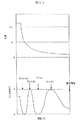
図14に、モニタ光を信号光の半分の波長とした場合の液晶素子の位相と電圧、クロスニコルのモニタ光の出力の関係を示す。
液晶素子の場合には、飽和電圧を印加すると位相シフト量が0に近くなる。
平行配向液晶は、そのギャップと充填する液晶のΔnによって、位相変化量を調整できる。
約10μmのギャップで、Δnが約0.25の液晶を充填すると位相シフト(変化)量は約2.2πとなり、本発明のように、0からπ変化させるには十分である。
電圧を十分印加(約10V)してモニタ出力が最低になった時の電圧を飽和電圧とし、次に、ここから電圧を下げて、モニタ出力が最大になる電圧が1/4波長電圧(位相π/2)、さらに電圧を下げて出力が0になるときの電圧が1/2波長電圧(位相π)である。
さらに電圧を低下させて、再度出力が0になったときの電圧が位相2πあるいは0の電圧である。
このように手動で3つの電圧を設定し、この3つの電圧を繰り返し印加することによって、その組み合わせの出力から偏波状態をモニタすることが可能となる。
液晶の駆動電圧は通常5V程度であり、飽和電圧も10V程度であるので、これらの電圧を電源に記憶させて繰り返し電圧印加できる電源は、非常に安価である。
液晶の応答速度は数msであるので、ADコンバータも低速のものを用いることが可能である。
通常、ノートパソコンなどに接続できるUSBタイプのADコンバータのデータ取り込み速度は、10チャンネルから20チャンネルのもので1ms程度であるので、これらの安価なADコンバータを用いれば十分である。
但し、液晶素子の場合にはヒステリシスがでることがないので、印加電圧は上昇時でも下降時でも、電圧−位相特性は同じになる。
FIG. 14 shows the relationship between the phase and voltage of the liquid crystal element and the output of the crossed Nicols monitor light when the monitor light is half the wavelength of the signal light.
In the case of a liquid crystal element, the phase shift amount becomes close to 0 when a saturation voltage is applied.
The phase change amount of the parallel alignment liquid crystal can be adjusted by the gap and Δn of the liquid crystal to be filled.
When a liquid crystal having a gap of about 10 μm and Δn of about 0.25 is filled, the amount of phase shift (change) is about 2.2π, which is sufficient to change from 0 to π as in the present invention.
The voltage when the voltage is sufficiently applied (about 10 V) and the monitor output becomes the minimum is the saturation voltage, and then the voltage from which the monitor output is maximized is ¼ wavelength voltage (phase π / 2), and the voltage when the output is further reduced to 0 is a ½ wavelength voltage (phase π).
The voltage when the voltage is further lowered and the output becomes 0 again is the voltage of phase 2π or 0.
In this way, by manually setting three voltages and repeatedly applying these three voltages, it is possible to monitor the polarization state from the output of the combination.
Since the driving voltage of the liquid crystal is usually about 5V and the saturation voltage is also about 10V, a power source that can store these voltages in the power source and repeatedly apply a voltage is very inexpensive.
Since the response speed of the liquid crystal is several ms, it is possible to use a low-speed AD converter.
Normally, the data acquisition speed of a USB type AD converter that can be connected to a notebook computer or the like is about 1 ms for 10 to 20 channels, so it is sufficient to use these inexpensive AD converters.
However, in the case of a liquid crystal element, since hysteresis does not occur, the voltage-phase characteristics are the same whether the applied voltage is rising or falling.
液晶素子の場合には、モニタ光を用いなくても、簡易に位相をキャパシタンスによってモニタすることが可能である。
その方法を以下に説明する。この方法は、液晶可変波長フィルタの波長(位相)とキャパシタンスが1:1に対応することを応用したものである。(K.Hirabayashi "Relationship between optical and electrics properties of LC optical devices," Opt.Lett.,21(1996)pp.1484-1486参照)
液晶素子中の液晶分子を、図15(a)のように示すと、入射光の感じる屈折率は、p偏波、s偏波それぞれに対して、下記(9)式の通りとなる。
[数8]
p:ne=一Δn×sin2(φ)+ηo
s:no
・・・・・・・・・・・・・・・・・・・・・ (9)
さらに、液晶素子の誘電率は、印加電界に対して、下記(10)式の通りとなる。
[数9]
εe=Δε×cos2(φ)+εo
・・・・・・・・・・・・・・・・・・・・・ (10)
従って、下記(11)式のように表される。
[数10]
(−(ne−no)/Δmax+(εe−εo)/Δmax)=1
・・・・・・・・・・・・・・・・・・・・・ (11)
液晶素子のキャパシタンスCは、C=εeS/dで表される。ここで、dはセルギャップ、Sは面積である。
従って、キャパシタンスの変化ΔCと位相の変化Δnは下記(12)式の関係で表される。
[数11]
Δn=−(Δnmax/ΔCmax)ΔC+Δnmax
・・・・・・・・・・・・・・・・・・・・・ (12)
In the case of a liquid crystal element, the phase can be easily monitored by capacitance without using monitor light.
The method will be described below. This method is an application of the fact that the wavelength (phase) and capacitance of the liquid crystal variable wavelength filter correspond to 1: 1. (See K.Hirabayashi "Relationship between optical and electrics properties of LC optical devices," Opt. Lett., 21 (1996) pp.1484-1486)
When the liquid crystal molecules in the liquid crystal element are shown as shown in FIG. 15A, the refractive index perceived by the incident light is expressed by the following equation (9) for each of the p-polarized light and the s-polarized light.
[Equation 8]
p: n e = one Δn × sin 2 (φ) + η o
s: n o
・ ・ ・ ・ ・ ・ ・ ・ ・ ・ ・ ・ ・ ・ ・ ・ (9)
Furthermore, the dielectric constant of the liquid crystal element is expressed by the following formula (10) with respect to the applied electric field.
[Equation 9]
ε e = Δε × cos 2 (φ) + ε o
・ ・ ・ ・ ・ ・ ・ ・ ・ ・ ・ ・ ・ ・ ・ ・ (10)
Therefore, it is expressed as the following equation (11).
[Equation 10]
(− (N e −n o ) / Δ max + (ε e −ε o ) / Δ max ) = 1
・ ・ ・ ・ ・ ・ ・ ・ ・ ・ ・ ・ ・ ・ ・ ・ (11)
The capacitance C of the liquid crystal element is expressed by C = ε e S / d. Here, d is a cell gap and S is an area.
Accordingly, the change ΔC in capacitance and the change Δn in phase are expressed by the following equation (12).
[Equation 11]
Δn = − (Δn max / ΔC max ) ΔC + Δn max
・ ・ ・ ・ ・ ・ ・ ・ ・ ・ ・ ・ ・ ・ ・ ・ (12)
図15(b)に示すように、Δnは電圧印加とともに減少して、0に近づき、ΔCは増大する。
従って位相Δは、下記(13)式のように簡単な式で表される。
[数12]
Δ=(−(Δnmax/ΔCmax)ΔC+Δnmax)×(d/nλ)
Δ=a×C+b
・・・・・・・・・・・・・・・・・・・・・ (13)
予め、液晶素子の位相シフト量とキャパシタンスを実測して、図16の関係を求めて置けば、aとbの値がわかり、キャパシタンスを測定するのみで、位相を求めることができる。この関係は温度が変化しても有効に成り立つ。
液晶素子のキャパシタンスは数nFであるので、温度依存性が少なく正確にキャパシタンスがわかっているコンデンサを液晶素子に直列に接続し、液晶とこのコンデンサに印加される印加電圧を測定することによって、キャパシタンスを実測できる。
この位相シフト量が、0、π/2、π/4になる電圧に設定し、この電圧を繰り返して液晶素子1、2に印加して、その時のディテクタの出力から偏波状態を算出することができる。
As shown in FIG. 15B, Δn decreases with voltage application, approaches 0, and ΔC increases.
Therefore, the phase Δ is expressed by a simple expression such as the following expression (13).
[Equation 12]
Δ = (− (Δn max / ΔC max ) ΔC + Δn max ) × (d / nλ)
Δ = a × C + b
・ ・ ・ ・ ・ ・ ・ ・ ・ ・ ・ ・ ・ ・ ・ ・ (13)
If the phase shift amount and capacitance of the liquid crystal element are measured in advance and the relationship shown in FIG. 16 is obtained, the values of a and b can be known, and the phase can be obtained simply by measuring the capacitance. This relationship is valid even if the temperature changes.
Since the capacitance of the liquid crystal element is several nF, a capacitor that is less dependent on temperature and whose capacitance is accurately known is connected in series to the liquid crystal element, and the capacitance is measured by measuring the liquid crystal and the applied voltage applied to the capacitor. Can be measured.
The phase shift amount is set to a voltage of 0, π / 2, π / 4, this voltage is repeatedly applied to the
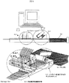
また、図17に示すように、ファイバアレイ、あるいは、導波路アレイからのアレイ状の信号光をアレイレンズでコリメートアレイにして、その光をディテクタアレイ(12−9)で受光することにより、アレイ状の信号光の偏波状態をモニタすることが可能となる。
図17では、4チャンネルの場合を図示しているが、市販のADコンバータは8チャンネル、16チャンネルのものが安価で市販されており、また、ディテクタアレイ(12−9)は40チャンネルのものも市販されているので、それらのADコンバータを用いることにより、8チャンネル、16チャンネルの偏波モニタを実現することが可能である。
以上説明したように、本実施例の偏波状態測定器によれば、電気光学効果を持つ位相制御素子(例えば、ニオブ酸リチウムを代表とする電気光学結晶、PLZTを代表とする電気光学セラミクス、液晶素子)による光ビームの位相シフト量を、モニタ光を用いることにより、正確に0、π/2、πに繰り返し設定して、その後ろに設けた偏光子付きのディテクタの出力から偏波状態を計算するようにしたので、従来の偏波状態測定器に比べて、安価であるとともに、小型化、かつ、アレイ化が可能となる。
以上、本発明者によってなされた発明を、前記実施例に基づき具体的に説明したが、本発明は、前記実施例に限定されるものではなく、その要旨を逸脱しない範囲において種々変更可能であることは勿論である。
Further, as shown in FIG. 17, the arrayed signal light from the fiber array or waveguide array is made into a collimated array by an array lens, and the light is received by the detector array (12-9). It becomes possible to monitor the polarization state of the signal light.
In FIG. 17, the case of 4 channels is illustrated, but commercially available AD converters of 8 channels and 16 channels are commercially available at low cost, and the detector array (12-9) is of 40 channels. Since these are AD converters, 8-channel and 16-channel polarization monitors can be realized.
As described above, according to the polarization state measuring instrument of the present embodiment, a phase control element having an electro-optic effect (for example, an electro-optic crystal typified by lithium niobate, an electro-optic ceramic typified by PLZT, The phase shift amount of the light beam by the liquid crystal element) is repeatedly set to 0, π / 2, and π accurately by using the monitor light, and the polarization state is output from the output of the detector with the polarizer provided behind it. Therefore, it is cheaper than the conventional polarization state measuring instrument, and it is possible to reduce the size and form an array.
As mentioned above, the invention made by the present inventor has been specifically described based on the above embodiments. However, the present invention is not limited to the above embodiments, and various modifications can be made without departing from the scope of the invention. Of course.
1−1 ハーフミラー
1−2 ファイバアレイを固定するV溝アレイ
1−3 テープファイバ
1−4 溝
1−5 プリズムマイクロレンズアレイ
1−6 ディテクタアレイ
1−7 プリズムマイクロレンズアレイでコリメートされたビームアレイ
1−8 ファイバコア
1−9 プリズム面に形成されたARコート
1−10 ディスクフィルタ
1−11 ファイバアレイとディテクタアレイを固定するジグ
1−12 ディスクフィルタの位置をモニタするセンサ部
1−13 円周上に設けたマーカ
2−1 2列のディテクタアレイ
2−2 平坦なガラス
2−3 透明電極
2−4 誘電体ミラー
2−5 ネマチック液晶
2−6 ミラー
2−7 λ/4板
2−8 入射する光ビーム
2−9 三角支持台
2−10 プリズム状に加工されたレンズアレイ
2−11 偏光分離素子
2−12 λ/2板
2−13 液晶フィルタを通過する光ビームアレイ
2−14 容量をモニタするための分轄された透明電極パターン
2ー15 液晶フィルタを駆動するための透明電極パターン
3−1 平面マイクロレンズアレイ基板
3−2 プリズムマイクロレンズアレイ
3−3 ファイバ
3−4 ハーフミラー
3−5 プリズムマイクロレンズアレイでコリメートされたビームアレイ
3−6 薄く研磨された平面マイクロレンズアレイ
3−7 プリズム
4−1 直線偏光子
4−2 45°方向の直線偏光子
4−3 上側に配置した直線偏光子
4−4 下側に配置したλ/4板
4−5 90°方向の直線偏光子
4−6 回転式円盤
4−7 破線マーカ
4−8 破線マーカで円盤の回転角度をモニタする部分
4−9 ディテクタアレイ
4−10 ハーフミラー
4−11 テープファイバ
4−12 プリズム台
4−13 出射側テープファイバ
5−1 ハーフミラー
5−2 ディテクタアレイ
5−3 V溝アレイを形成したガラス基板
5−4 溝
5−5 テープファイバ
5−6 直線偏光子
5−7 直線偏光子の偏光軸の方向
5−8 プリズムマイクロレンズアレイ
6−1 円盤状に加工した直線偏光子
6−2 偏光子の軸の方向をモニタするためのマーカ
6−3 ディテクタアレイ
6−4 マーカモニタ
6−5 ファイバアレイを固定したV溝ガラス基板
6−6 ハーフミラー
6−7 プリズムマイクロレンズアレイ
6−8 ファイバアレイから反射されてコリメートされた光ビームアレイ
6−9 固定ジグ
8−1 グレーティング
8−2 レンズ
8−3 2次元ディテクタアレイ
8−4 プリズムレンズアレイ
8−5 ハーフミラー
8−6 テープファイバ
8−7 分光した光
9−1 光導波路の光導入部
9−2 実施例3で作製したインライン形偏光子ディテクタアレイ
9−3 偏波制御回路
10 コリメートレンズ
11−1 電気光学セラミクス(PLZT)
11−2 電極
11−3 導波路あるいはファイバを固定する固定板
11−4 導波路あるいはファイバのコア
11−5 誘電体ミラー
11−6 プリズム
11−7 平面マイクロレンズ(またはマクロレンズ)
11−8 偏光分離素子(方解石あるいは偏光ビームスプリッタ)
11−9 ディテクタ
11−10 三角形状の台
11−11 入出力ファイバ
11−12 誘電体ミラーで反射された光ビーム
11−13 モニタ光を作るコリメータ付きレーザダイオード
11−14 モニタビーム
11−15 ディテクタ
11−16 直線偏光子
11−17 直線偏光子
11−18 パルス電源
11 入出力ファイバ
12−1 平行配向液晶素子
12−2 入射光ビーム
12−3 直線偏光子
12−4 ディテクタ
12−5 直線偏光子
12−6 直線偏光子
12−7 モニタ用レーザあるいは発光ダイオード
12−8 パルス電源
12−9 ディテクタアレイ
1-1 Half mirror 1-2 V-groove array for fixing fiber array 1-3 Tape fiber 1-4 Groove 1-5 Prism microlens array 1-6 Detector array 1-7 Beam array collimated by prism microlens array 1-8 Fiber core 1-9 AR coating formed on prism surface 1-10 Disc filter 1-11 Jig for fixing fiber array and detector array 1-12 Sensor unit for monitoring position of disc filter 1-13 Circumference Marker provided on 2-1 Detector array in two rows 2-2 Flat glass 2-3 Transparent electrode 2-4 Dielectric mirror 2-5 Nematic liquid crystal 2-6 Mirror 2-7 λ / 4 plate 2-8 Incident 2-9 Triangular support base 2-10 Lens array processed into a prism shape 2-11 Polarization component Releasing element 2-12 λ / 2 plate 2-13 Light beam array passing through liquid crystal filter 2-14 Demarcated transparent electrode pattern for monitoring capacity 2-15 Transparent electrode pattern for driving liquid crystal filter 3- DESCRIPTION OF SYMBOLS 1 Planar microlens array substrate 3-2 Prism microlens array 3-3 Fiber 3-4 Half mirror 3-5 Beam array collimated by prism microlens array 3-6 Thinly polished planar microlens array 3-7 Prism 4-1 Linear polarizer 4-2 Linear polarizer in 45 ° direction 4-3 Linear polarizer arranged on the upper side 4-4 λ / 4 plate arranged on the lower side 4-5 Linear polarizer in the 90 ° direction 4- 6 Rotating disk 4-7 Dotted line marker 4-8 Part for monitoring rotation angle of disk with broken line marker 4-9 Detector array 4-10 Mirror 4-11 Tape fiber 4-12 Prism stage 4-13 Output side tape fiber 5-1 Half mirror 5-2 Detector array 5-3 Glass substrate on which V-groove array is formed 5-4 Groove 5-5 Tape fiber 5- 6 Linear Polarizer 5-7 Direction of Polarization Axis of Linear Polarizer 5-8 Prism Microlens Array 6-1 Linear Polarizer Processed in Disk Shape 6-2 Marker for Monitoring Direction of Axis of Polarizer 6- 3 Detector Array 6-4 Marker Monitor 6-5 V Groove Glass Substrate with Fixed Fiber Array 6-6 Half Mirror 6-7 Prism Microlens Array 6-8 Collimated Light Beam Array 6-9 Fixed jig 8-1 Grating 8-2 Lens 8-3 Two-dimensional detector array 8-4 Prism lens array A 8-5 Half mirror 8-6 Tape fiber 8-7 Spectroscopyed light 9-1 Optical light guide part 9-2 In-line polarizer detector array produced in Example 3 9-3 Polarization control circuit 10 Collimator Lens 11-1 Electro-Optical Ceramics (PLZT)
11-2 Electrode 11-3 Fixing Plate for Fixing Waveguide or Fiber 11-4 Waveguide or Fiber Core 11-5 Dielectric Mirror 11-6 Prism 11-7 Planar Micro Lens (or Macro Lens)
11-8 Polarization separation element (calcite or polarization beam splitter)
11-9 Detector 11-10 Triangular Base 11-11 I / O Fiber 11-12 Light Beam Reflected by Dielectric Mirror 11-13 Laser Diode with Collimator for Making Monitor Light 11-14 Monitor Beam 11-15 Detector 11 -16 Linear polarizer 11-17 Linear polarizer 11-18
Claims (17)
前記光取出手段で取り出された信号光をコリメートして光ビームとする光コリメート手段と、
前記光ビームが垂直に入射される偏波制御手段と、
前記偏波制御手段を通過した光が入射されるディテクタアレイとを有し、
前記光取出手段は、ファイバあるいは導波路内の光を通過する部分を切断するように、前記ファイバあるいは導波路の延長方向に垂直な直線に対して、22.5°の角度で斜めに、前記ファイバあるいは導波路に設けられる第1の溝と、
当該第1の溝内に挿入されるハーフミラーとを有し、
前記光コリメート手段は、前記ハーフミラーで反射された光を、コリメートして出射するプリズム状のレンズアレイであることを特徴とする偏波状態測定器。 Light extraction means for extracting at least part of the signal light in the fiber or waveguide to the outside;
A light collimating means for collimating the signal light extracted by the light extracting means into a light beam;
Polarization control means on which the light beam is vertically incident;
Possess a detector array light passing through the polarization control means is incident,
The light extraction means is inclined at an angle of 22.5 ° with respect to a straight line perpendicular to the extending direction of the fiber or waveguide so as to cut a portion of the fiber or waveguide through which light passes. A first groove provided in the fiber or waveguide;
A half mirror inserted into the first groove,
The polarization state measuring device , wherein the light collimating means is a prism-shaped lens array that collimates and emits the light reflected by the half mirror .
前記円盤上に設けられる、0°方向の偏光子、45°方向の偏光子、λ/4板+90°方向の偏光子、および90°方向の偏光子、あるいは任意の方向の直交する偏光子2枚および波長板を備えた偏光子を有することを特徴とする請求項1または請求項2に記載の偏波状態測定器。 The polarization control means includes a disk having a rotation mechanism,
A 0 ° -direction polarizer, a 45 ° -direction polarizer, a λ / 4 plate + 90 ° -direction polarizer, a 90 ° -direction polarizer, or an orthogonal polarizer 2 provided on the disk. The polarization state measuring device according to claim 1, further comprising a polarizer including a sheet and a wave plate.
前記第2の溝に挿入されるアクティブ面型素子とを有することを特徴とする請求項1ないし請求項4のいずれか1項に記載の偏波状態測定器。 A second groove provided in the fiber or waveguide so as to cut a portion of the fiber or waveguide through which light passes;
The polarization state measuring instrument according to any one of claims 1 to 4 , further comprising an active surface element inserted into the second groove.
前記位相制御素子の後段に配置され、p偏波とs偏波に分離する偏光分離素子とを有し、
前記ディテクタアレイは、前記偏光分離素子の前記2つの偏波の出力部に配置される2個のディテクタであり、
前記mを3つ以上ふって、前記位相制御素子を通過する光ビームの位相をシフトさせた時の前記2個のディテクタの出力に基づき、光ビームの偏光状態を測定する測定手段とを備えることを特徴する請求項1に記載の偏波状態測定器。 The polarization control means is arranged at a position where the light beam is incident so that the axis is in an arbitrary direction, and when m and n are integers, the phase of the light beam passing therethrough is 2nπ + mπ / 4. A phase control element that only shifts,
A polarization separation element that is disposed downstream of the phase control element and separates into p-polarization and s-polarization;
The detector array is two detectors arranged at the output portions of the two polarized waves of the polarization separation element,
Measuring means for measuring the polarization state of the light beam based on the outputs of the two detectors when the phase of the light beam passing through the phase control element is shifted by passing three or more m The polarization state measuring device according to claim 1, wherein:
前記第1および第2の位相制御素子の後段に、軸が前記任意の方向となるように配置される直線偏光子とを有し、
前記ディテクタアレイは、前記直線偏光子の後段に配置されるディテクタであり、
前記k、mをそれぞれ3つ以上ふって、前記第1および第2の位相制御素子を通過する光ビームの位相をシフトさせたときの、前記第1の位相制御素子を通過する光ビームの位相シフト量と前記第2の位相制御素子を通過する光ビームの位相シフト量との組み合わせの中の少なくとも6つの組み合わせの時の、前記ディテクタの出力に基づき、光ビームの偏光状態を測定する測定手段とを備えることを特徴する請求項1に記載の偏波状態測定器。 The polarization control means is disposed at a position where the light beam is incident so that each axis has a ± θ direction with respect to an arbitrary direction, and k, l, m, and n are integers. First and second phase control elements for shifting the phase of the light beam passing therethrough by 2nπ + mπ / 4 and 2lπ + kπ / 4;
A linear polarizer disposed behind the first and second phase control elements so that the axis is in the arbitrary direction;
The detector array is a detector disposed at a subsequent stage of the linear polarizer,
The phase of the light beam passing through the first phase control element when the phase of the light beam passing through the first and second phase control elements is shifted by passing three or more k and m, respectively. Measuring means for measuring the polarization state of the light beam based on the output of the detector at the time of at least six combinations of the shift amount and the phase shift amount of the light beam passing through the second phase control element The polarization state measuring device according to claim 1 , further comprising:
前記任意の方向は、前記固定板の第1の面の法線方向であり、
前記位相制御素子は、前記固定板の第1の面上に配置されることを特徴とする請求項6ないし請求項9のいずれか1項に記載の偏波状態測定器。 A fixing plate for fixing the fiber or waveguide;
The arbitrary direction is a normal direction of the first surface of the fixing plate;
10. The polarization state measuring instrument according to claim 6 , wherein the phase control element is disposed on a first surface of the fixed plate. 11.
前記モニタ光を受光するモニタ光用ディテクタと、
前記位相制御素子のモニタ光の入射面および出射面に配置されるクロスニコル状態の偏光子とを備え、
前記位相制御素子は、印加電圧により位相シフト量を変化させる位相制御素子であり、
前記モニタ光は、前記信号光と同じ波長あるいはその半分の波長の光であり、
前記測定手段は、前記モニタ光ディテクタの出力が、最大あるいは最小となる印加電圧を、前記位相制御素子を通過する光ビームの位相シフト量が、2nπ+mπ/4となる電圧として記憶しておき、前記記憶した電圧を前記位相制御素子に印加し、前記位相制御素子を通過する光ビームの位相をシフトさせて、光ビームの偏光状態を測定することを特徴とする請求項6ないし請求項11のいずれか1項に記載の偏波状態測定器。 A monitor light source that allows monitor light parallel to the light beam to pass through a portion other than the light beam of the phase control element;
A monitor light detector for receiving the monitor light;
A polarizer in a crossed Nicol state disposed on the incident surface and the exit surface of the monitor light of the phase control element,
The phase control element is a phase control element that changes a phase shift amount by an applied voltage,
The monitor light is light having the same wavelength as the signal light or a half wavelength thereof,
The measuring means stores an applied voltage at which the output of the monitor light detector is maximized or minimized as a voltage at which a phase shift amount of a light beam passing through the phase control element is 2nπ + mπ / 4, applying the stored voltage to the phase control element, wherein by shifting the phase of the light beam passing through the phase control element, one of the claims 6 to 11, characterized in that measuring the polarization state of the light beam The polarization state measuring instrument according to claim 1.
前記位相制御素子の軸は、前記電気光学結晶板の結晶軸方向であることを特徴とする請求項6ないし請求項13のいずれか1項に記載の偏波状態測定器。 The phase control element is an electro-optic crystal plate;
The polarization state measuring device according to any one of claims 6 to 13 , wherein an axis of the phase control element is a crystal axis direction of the electro-optic crystal plate.
前記位相制御素子の軸は、前記電気光学セラミクス板に印加する電界方向であることを特徴とする請求項6ないし請求項13のいずれか1項に記載の偏波状態測定器。 The phase control element is an electro-optic ceramic plate;
The polarization state measuring instrument according to any one of claims 6 to 13 , wherein an axis of the phase control element is a direction of an electric field applied to the electro-optic ceramic plate.
前記位相制御素子の軸は、前記液晶素子の液晶分子の配向方向であることを特徴とする請求項6ないし請求項13のいずれか1項に記載の偏波状態測定器。 The phase control element is a liquid crystal element,
The polarization state measuring device according to any one of claims 6 to 13 , wherein an axis of the phase control element is an alignment direction of liquid crystal molecules of the liquid crystal element.
前記液晶素子のキャパシタンスを測定する測定手段を備え、
前記測定手段の測定結果に基づき、前記位相制御素子を通過する前記光ビームの位相シフト量を、2nπ+mπ/4に制御することを特徴とする請求項6ないし請求項13のいずれか1項に記載の偏波状態測定器。 The phase control element is a liquid crystal element,
Measuring means for measuring the capacitance of the liquid crystal element,
Based on the measurement result of the measuring means, wherein the phase shift amount of the light beam passing through the phase control element, in any one of claims 6 to 13, characterized in that controlling the 2nπ + mπ / 4 Polarization state measuring instrument.
Priority Applications (1)
| Application Number | Priority Date | Filing Date | Title |
|---|---|---|---|
| JP2003275503A JP4108564B2 (en) | 2002-07-26 | 2003-07-16 | Polarization state measuring instrument |
Applications Claiming Priority (2)
| Application Number | Priority Date | Filing Date | Title |
|---|---|---|---|
| JP2002218458 | 2002-07-26 | ||
| JP2003275503A JP4108564B2 (en) | 2002-07-26 | 2003-07-16 | Polarization state measuring instrument |
Publications (2)
| Publication Number | Publication Date |
|---|---|
| JP2004170382A JP2004170382A (en) | 2004-06-17 |
| JP4108564B2 true JP4108564B2 (en) | 2008-06-25 |
Family
ID=32715524
Family Applications (1)
| Application Number | Title | Priority Date | Filing Date |
|---|---|---|---|
| JP2003275503A Expired - Fee Related JP4108564B2 (en) | 2002-07-26 | 2003-07-16 | Polarization state measuring instrument |
Country Status (1)
| Country | Link |
|---|---|
| JP (1) | JP4108564B2 (en) |
Families Citing this family (5)
| Publication number | Priority date | Publication date | Assignee | Title |
|---|---|---|---|---|
| JP4770913B2 (en) * | 2008-11-13 | 2011-09-14 | 横河電機株式会社 | Optical fiber characteristic measuring apparatus and optical fiber characteristic measuring method |
| JP7103081B2 (en) * | 2018-08-31 | 2022-07-20 | 住友電気工業株式会社 | Fiber optic array and optical measuring device |
| JP7604100B2 (en) * | 2020-01-07 | 2024-12-23 | 浜松ホトニクス株式会社 | Spectroscopic Module |
| CN113465887B (en) * | 2021-06-24 | 2022-05-20 | 华中科技大学 | Inversion method and device for exciton characteristic parameters of light-emitting device |
| CN116105980B (en) * | 2023-01-13 | 2025-08-01 | 中国人民解放军国防科技大学 | Method for directly measuring polarization extinction ratio of linear polarization supercontinuum laser source |
-
2003
- 2003-07-16 JP JP2003275503A patent/JP4108564B2/en not_active Expired - Fee Related
Also Published As
| Publication number | Publication date |
|---|---|
| JP2004170382A (en) | 2004-06-17 |
Similar Documents
| Publication | Publication Date | Title |
|---|---|---|
| US5111321A (en) | Dual-polarization liquid-crystal etalon filter | |
| US7085492B2 (en) | Wavelength division multiplexed device | |
| JP2587743B2 (en) | Tunable liquid crystal etalon filter | |
| US6978062B2 (en) | Wavelength division multiplexed device | |
| EP1370900B1 (en) | Fiber optical attenuator | |
| JP2925064B2 (en) | Tunable wavelength filter | |
| US8254732B2 (en) | Phase modulator and optical modulation device | |
| US5889900A (en) | Integrated optic tunable filters and their methods of fabrication and use | |
| EP2823343A1 (en) | Active alignment of optical fiber to chip using liquid crystals | |
| JP2004510172A (en) | Apparatus and method for reducing polarization sensitivity with a diffraction grating used in an optical fiber communication device | |
| CN101681030A (en) | Optical waveform shaping device | |
| CN114838824A (en) | A Microchip Spectrometer with Large Bandwidth and High Resolution | |
| JP4108564B2 (en) | Polarization state measuring instrument | |
| JP2004226501A (en) | Variable optical attenuator | |
| JP5669140B2 (en) | Optical performance monitor | |
| US6718076B2 (en) | Acousto-optic tunable filter with segmented acousto-optic interaction region | |
| CN102096217B (en) | Adjustable dispersion compensation device based on liquid crystal array technology | |
| US7146076B2 (en) | Diffractive optical element and optical device using the same | |
| US20050174919A1 (en) | Optical polarization controller | |
| JPH085976A (en) | Tunable wavelength optical filter | |
| JP2003083810A (en) | Spectroscopic device and light measuring device | |
| JP4823584B2 (en) | Light modulator | |
| US8619216B1 (en) | Optical wavelength filter | |
| JPH085977A (en) | Variable wavelength liquid crystal optical filter | |
| JP2005091982A (en) | Optical module, optical attenuator |
Legal Events
| Date | Code | Title | Description |
|---|---|---|---|
| A621 | Written request for application examination |
Free format text: JAPANESE INTERMEDIATE CODE: A621 Effective date: 20050711 |
|
| A977 | Report on retrieval |
Free format text: JAPANESE INTERMEDIATE CODE: A971007 Effective date: 20070920 |
|
| A131 | Notification of reasons for refusal |
Free format text: JAPANESE INTERMEDIATE CODE: A131 Effective date: 20071016 |
|
| A521 | Written amendment |
Free format text: JAPANESE INTERMEDIATE CODE: A523 Effective date: 20071217 |
|
| TRDD | Decision of grant or rejection written | ||
| A01 | Written decision to grant a patent or to grant a registration (utility model) |
Free format text: JAPANESE INTERMEDIATE CODE: A01 Effective date: 20080401 |
|
| A61 | First payment of annual fees (during grant procedure) |
Free format text: JAPANESE INTERMEDIATE CODE: A61 Effective date: 20080402 |
|
| FPAY | Renewal fee payment (event date is renewal date of database) |
Free format text: PAYMENT UNTIL: 20110411 Year of fee payment: 3 |
|
| R150 | Certificate of patent or registration of utility model |
Free format text: JAPANESE INTERMEDIATE CODE: R150 |
|
| FPAY | Renewal fee payment (event date is renewal date of database) |
Free format text: PAYMENT UNTIL: 20120411 Year of fee payment: 4 |
|
| FPAY | Renewal fee payment (event date is renewal date of database) |
Free format text: PAYMENT UNTIL: 20130411 Year of fee payment: 5 |
|
| LAPS | Cancellation because of no payment of annual fees |