JP4106109B2 - General purpose power supply for multiple loads - Google Patents
General purpose power supply for multiple loads Download PDFInfo
- Publication number
- JP4106109B2 JP4106109B2 JP22323597A JP22323597A JP4106109B2 JP 4106109 B2 JP4106109 B2 JP 4106109B2 JP 22323597 A JP22323597 A JP 22323597A JP 22323597 A JP22323597 A JP 22323597A JP 4106109 B2 JP4106109 B2 JP 4106109B2
- Authority
- JP
- Japan
- Prior art keywords
- switch
- inductor
- frequency
- power
- capacitor
- Prior art date
- Legal status (The legal status is an assumption and is not a legal conclusion. Google has not performed a legal analysis and makes no representation as to the accuracy of the status listed.)
- Expired - Fee Related
Links
Images


Classifications
-
- H—ELECTRICITY
- H05—ELECTRIC TECHNIQUES NOT OTHERWISE PROVIDED FOR
- H05B—ELECTRIC HEATING; ELECTRIC LIGHT SOURCES NOT OTHERWISE PROVIDED FOR; CIRCUIT ARRANGEMENTS FOR ELECTRIC LIGHT SOURCES, IN GENERAL
- H05B6/00—Heating by electric, magnetic or electromagnetic fields
- H05B6/02—Induction heating
- H05B6/04—Sources of current
-
- H—ELECTRICITY
- H05—ELECTRIC TECHNIQUES NOT OTHERWISE PROVIDED FOR
- H05B—ELECTRIC HEATING; ELECTRIC LIGHT SOURCES NOT OTHERWISE PROVIDED FOR; CIRCUIT ARRANGEMENTS FOR ELECTRIC LIGHT SOURCES, IN GENERAL
- H05B6/00—Heating by electric, magnetic or electromagnetic fields
- H05B6/02—Induction heating
- H05B6/06—Control, e.g. of temperature, of power
Description
【0001】
【産業上の利用分野】
本発明は、一般に、電力制御システムに関するものであり、とりわけ、スイッチング電源及び融着システムが入力回路要素を共用できるようにする構成に関するものである。
【0002】
【従来の技術】
ほぼ1984年に始まり、低コストのパーソナル・レーザ・プリンタが利用可能になってきた。乾式電子写真コピー機及びプリンタの全てが、ドライ・トナーを利用してイメージの現像を行っている。典型的なトナーは、静電潜像の現像にとって望ましい摩擦充電特性をトナーに付与する、スチレン・アクリル樹脂、一般にはカーボン・ブラックである顔料、電荷制御染料から構成される。スチレン・アクリル樹脂は、溶融させて、一般には紙である所望の媒体に融着させることが可能な、熱可塑性プラスチックである。
【0003】
乾式電子写真システムが世界中で動作できるようにするためには、50Hz〜60Hzの周波数で、90Vrms〜240Vrmsを供給するAC電源システムにおいて、満足のゆく動作が可能でなければならない。AC電源は、電子写真システム内の2つの主たるサブ・システムを動作させる。スイッチング電源が、電子装置、モータ、及び、ディスプレイに電力を供給する。スイッチング電源に関する電力要件は、さまざまであるが、一般には、100ワット未満である。電子写真システムにおける第2の主たるサブ・システムは、融着システムである。典型的な融着システムは、現像されたイメージを備える印刷媒体がその間を通過する時、トナーを溶融し、圧力によって、溶融熱可塑性プラスチックを物理的に媒体に融着させる、2つの加熱プラテン・ローラから構成される。加熱は、通常、高出力タングステン・フィラメント石英ランプを中空のプラテン・ローラ内部に配置することによって実施される。スイッチング電源の場合と同様、融着システムの電力要件は、プリンタによってさまざまであるが、ほぼ1,000ワットほどである。
【0004】
電子写真プリンタ、スイッチング電源、融着システム、及び、電力電子装置の組み合わせは、International Electrical Commission(IEC)の電流高調波及びフリッカに関する規定IEC555−2およびIEC555−3を満たさなければならない。プリンタは、Federal Communications Commission(FCC)の電力線による伝導放出及び放射性放出に関するクラスBの規定に合格しなければならない。さらに、プリンタは、CISPRの電力線による伝導放出及び放射性放出に関するB要件に合格しなければならない。最後に、プリンタは、オフィス環境において、人間の可聴範囲内の複音または単音を過度に放射するという欠点を備えていてはならない。電子写真システムは、EPAエネルギ・スター・プログラムによって示唆されているエネルギの節約のため、パワー・ダウンまたはパワー・オフ・モードにスイッチング可能でなければならない。
【0005】
本発明より以前の力率補正タイプのスイッチング電源には、電流の波形に事前調整及び整形を施して、正弦波に近くなり、入力電圧と同相をなすようにするため、「フロント・エンド」にブースト調整器が配置されているのが最も一般的であった。こうした構成は、かなりの出力変換損失を生じる可能性がある。さらに、ブースト変換器に必要とされる追加電子装置のコストが、総コストに悪影響を及ぼすことになる。もう1つの解決策は、力率が極めてよいが、過度のフリッカを被り、汎用融着器を備えていない、標準的なトライアック・ベースの融着器コントローラの場合、AC電源に並列に接続された力率補正タイプのスイッチ・モード電源から構成された。
【0006】
【発明が解決しようとする課題】
本発明は、スイッチング電源及び融着システムが単一の共通AC電源を共用することのできる回路構成を提供することを目的とする。
【0007】
【課題を解決するための手段】
本発明によれば、加熱素子を所望の温度まで加熱し、単一の共通AC電源から出力を発生するための回路が得られる。まず、AC電力は、整流器によってDC電力に変換される。インダクタ及びコンデンサは、AC電力周波数を超える共振周波数を有している。
【0008】
加熱素子及び整流器に、スイッチが接続される。次に、コントローラが、所望の温度の指示と共に加熱素子の実際の温度を示す信号を受信する。コントローラは、誤差信号を発生し、該信号によって、スイッチが切れたり、入ったりして、加熱素子が所望の温度まで加熱される。変圧器及び整流器に、もう1つのスイッチが接続されている。独立したコントローラが、第2のスイッチを切ったり、入れたりすることによって、変圧器の二次側から出力が発生する。2つのコントローラは、インダクタ及びコンデンサの共振周波数を超えるパルス幅変調周波数を利用する。
【0009】
変圧器の出力は、ダイオードによって整流され、その後、大形コンデンサによってフィルタリングが施される。コンデンサの両端間における中間電圧は、コントローラにフィードバックされ、これによって、PWM(パルス幅変調)信号が変更されて、中間電圧が調整を受ける。最後に、いくつかの電力変換器によって、中間電圧が所望の使用電圧に変換される。
【0010】
【実施例】
本発明は、本書に例示の特定の実施例に制限されるものではない。アトニー・ドケット番号が10950291−1の「A REDUCED FLICKERFUSING SYSTEM FOR USE IN ELECTROPHOTOGRAPHIC PRINTERS AND COPIERS」に詳述されている図1の回路は、ブースト変換器構成の入力インダクタLを利用して、変換器によって引き出される電流を平均することにより、ACラインに加えられる電流高調波を大幅に低減する。この構成によって、負荷Rfによって引き出される平均電流が線形に制御され、従って、負荷によって引き出される平均電力が、デューティ・サイクルに応じて線形に変動する。フィラメントRfが、PWM113によってスイッチされ、回路から外れると、コンデンサCが、入力フィルタ・インダクタL電流に対する連続電流経路を形成する。
【0011】
図2には、PWMの単純化された概略図が示されている。コントローラ110のタイプによっては、トランジスタMをスイッチすることによって、負荷のスイッチングを行い、回路に組み込んだり、回路から外したりするものもある。コントローラの正確な実施は、当該技術の熟練者には明らかなように、設計に固有のものである。
【0012】
パルス幅変調器のデューティ・サイクルを修正することによって、その電力要件の変化につれて負荷電圧に制御を加える、標準的なDC・DC電圧変換器とは異なり、この変換器は、プリンタの融着システムの加熱素子Rに供給されるAC電力、従って、融着システムの温度を制御する。
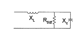
【0013】
図3の回路には、本発明の望ましい実施例の単純化された回路が示されている。フィルタ構成要素L及びC1と十分な大きさの抵抗電力負荷Rf及びRSPが適正に選択されると、入力ラインの基本周波数の半サイクル毎に、フィルタ・コンデンサC1が完全に放電し、入力インダクタLは、ほぼACの半サイクル全体にわたって連続して導通することになり、AC電源は、本質的に、抵抗負荷、すなわち、AC電圧源と同相の主電流に直面することになる。この結果、広範囲のデューティ・サイクル及びその関連する電力レベルにわたって、ほぼ1の力率が得られることになる。
【0014】
図3の電力変換器構成の場合、並列抵抗負荷Rf及びRSPは、ACの半サイクル毎に数百回スイッチングされて、回路に組み込まれたり、回路から外されたりするので、実効抵抗負荷が生じる。この実効抵抗負荷については、式1及び2に示すように、抵抗負荷に供給される電力とデューティ・サイクル・パルス幅変調によって消費される電力を同等とみなすことによって知ることができる。
Rf/df=Rf/df 式1
および、
RSP/dSP=RSP/dSP 式2
電力コントローラによってAC電源に加えられる実効抵抗負荷は:
【0015】
【数1】

ここで、dfはPWM113のデューティ・サイクルであり、dSPはPWM213のデューティ・サイクルである。
【0017】
従って、入力インダクタLが常に連続導通している限り、AC電源には、本質的に、PWMのデューティ・サイクルによって値が制御される抵抗が見える。連続導通を確保し、同時に、より高い周波数の放出のパワー・スペクトルを拡散させるためには、PWM113及びPWM213は、同相の可能性もあるが、スイッチングによって、互いに位相がずれるようにすべきである。
【0018】
電子写真プリンタに関連した電力レベルを約1kWに確実に制御するため、コンポーネントの選択には特に注意を払う必要がある。フィルタ構成要素の選択には、フィルタ構成要素のコストだけではなく、電流高調波、入力電力周波数、スイッチング周波数の制御を行う必要性についても考慮しなければならない。
【0019】
最適な動作を得るには、電流フィルタ・インダクタLは、いくつかの属性を備えていなければならない。インダクタLは、負荷の全電流を取り扱うので、第1の属性は、i2*Rの損失を最小限に押さえるために必要な極めて低い直列抵抗である。第2の属性は、インダクタLが、比較的小さく、このため、インダクタンス値が大きい場合、鉄またはフェライトのコアが必要になる。第3に、インダクタLは、極めて大きい飽和電流を備えなければならない。飽和を生じることなく、大電流、及び、結果生じる磁束密度を取り扱うということは、インダクタが鉄心によって構成されることを表している。第4に、伝導放出を最小限に押さえるため、インダクタは、巻線間の寄生容量が可能性のある最小値になるように設計しなければならない。最後に、インダクタのコアは、鉄損を最小限に抑えるように設計すべきである。
【0020】
フィルタ・コンデンサCは、コンデンサのタイプに影響を及ぼす困難な要求、及び、コンデンサが備えていなければならない定格に従う。フィルタ・コンデンサは、339ボルトを超える連続電圧に耐えることができなければならないし、160アンペアを超えるそれぞれのサージ電流に耐えなければならない。フィルタ・コンデンサは、PWMの各付勢及び消勢毎に、それぞれの大サージ電流にさらされる。コンデンサにおける過度の電力消費及び加熱を回避するため、フィルタ・コンデンサは、極めて小さい同等の直列抵抗ESRを示すことが望ましい。コンデンサが示すキャパシタンスは、変換器のデューティ・サイクルが変化する際に遭遇する可能性のある周波数範囲全体にわたって、ほぼ一定のままであることも望ましい。これらの要件を満たすため、モータ起動タイプのコンデンサが理想である。このタイプのコンデンサは、その属性を考慮すると、比較的安価であり、市販のACモータ用途において世界中で大量に利用されている。
【0021】
図3の電力制御構成のフィルタ構成要素は、
ω0=1/√(LC) 式4
の固有周波数ω0を備えた共振タンク回路を形成する。
【0022】
高調波電流の含有量が極めて少ないという所望の利点を得るには、電力フィルタの共振周波数ω0の位置が、できるだけ入力電力周波数ωPから離れるようにしなければならない。さらに、電力フィルタ構成要素によって形成される共振回路の励起を回避するため、電源スイッチのスイッチング周波数ωSの位置が、電力フィルタの共振周波数からできるだけ離れるようにすることが望ましい。電力フィルタの共振周波数の位置が、入力電力周波数より少なくとも1桁分高く、スイッチング周波数の位置が、電力フィルタの共振周波数より少なくとも1桁分高い場合、提示の電力変換器の構成によって、電力フィルタ・タンクの過度の励起が誘発されないだけでなく、電流高調波に対して極めて有効な制御が施されることになる。フィルタ共振周波数の位置決めに関する判定基準は、次のように表される
ωP<<ω0<<ωS 式5
【0023】
【数2】
さらに、AC電源に対してほぼ抵抗性の負荷を加えるためには、式6の判定基準を満たさなければならない。電源周波数50Hzまたは60Hzにおける入力インダクタのインピーダンスの大きさは、予測される抵抗負荷よりはるかに小さくなければならないし、フィルタ・コンデンサのインピーダンスの大きさは、予測される抵抗負荷よりはるかに大きくなければならない。
【0025】
電力フィルタのインダクタが、ほぼACの半サイクル全体にわたって連続導通する限りにおいて、力率は、変位力率によってほぼ完全に支配される。また、電力フィルタの共振周波数及びフィラメント・スイッチ周波数の位置が十分に離れている限りにおいて、スイッチング電流の高調波による電流歪みは、最小になり、電流歪み率cdfは、ほぼ1になる。
【0026】
力率PFは、一般に、変位力率dpfに電流歪み率cdfを掛けたものから成り、下記のように表される
PF=dpf・cdf 式7
ここで、変位力率は、インピーダンス位相角のコサイン、cos(θ)と定義される。
【0027】
電流歪みがないものと仮定すると、力率は、完全に変位力率によって決まることになり、負荷インピーダンス位相角θから簡単に計算される。従って、力率は、下記のように仮定される:
PF=cos(θ) 式8
【0028】
フィルタ・コンデンサの第1の通過選択(pass selection)は、電力の質が劣化し始める極めて低い負荷において実施することができる。まず、70ワットの想定電力レベルで、所望の力率が選択される。
PF=cos(θ)=0.99 式9
従って、
θ=8.11゜ 式10
また、70ワットの想定電力に関して、
Rf/df=Rf/df=V2/P=1202/70≒200Ω 式11
Cの値は、図4の助けによって求めることが可能である。回路のインピーダンスは:
【0029】
【数3】
しかし、インダクタンスの効果は、十分にわずかなものであるため、さしあたっては、排除することが可能である。従って、インピーダンスは、下記のようにして求めることが可能である:
【0031】
【数4】
従って:
θ=tan-1(虚部/実部) 式14
θ=tan-1[ωCRf/df] 式15
tan(θ)=ωCRf/df 式16
ここで、電源の周波数は、60Hzと仮定される。Cについて式16を解くと:
C=tan(θ)/(ωRf/df)=2μF 式17
【0033】
フィルタ・インダクタLの第1の通過選択は、任意の負荷で実施することが可能である。第1の通過選択は、特定の共振周波数を選んで実施される。
ω0=1/√(LC) 式18
【0034】
F0=7.9kHzを選択し、インダクタンスを解くと、200μHのインダクタに関する値が得られる。実際には、インダクタに指定することができる値が大きくなるほど、結果生じるフィルタリングを施された電流は良好になる。しかし、不必要な費用を回避するため、フィルタ・インダクタはできるだけ小さくするのが望ましい。やはり、伝導放出を最小限に抑えるため、インダクタは、巻線間において可能性のある寄生容量が最低になるように設計するのが望ましい。
【0035】
上記値を利用すると、力率は次のようになる:
Z=195.55−j29.4127=197.745∠−8.5゜ 式19
PF=cos(−8.5)=0.989 式20
【0036】
電源のモデルをReffに並列に配置することによって、図4の有効回路に電源負荷を加えることができる。図5には、これが示されている。60Hzにおいて、変圧器のインピーダンスは、ほぼ純粋に抵抗性である。従って、電源が35ワットを引き出すものと仮定すると、
RSP=1202/35=411Ω 式21
図5のインピーダンスは:
【0037】
【数5】
そして、力率は:
PF=cos(−5.76)=0.995 式23
【0039】
生じる可能性のある電流高調波は、LC電力フィルタ共振周波数から始まる。図3の望ましい実施例の場合、第1の電流高調波は、50HzのACシステムに関して第158高調波の近くで始まり、60HzのACシステムに関して第131高調波から始まる。他の電流高調波は、スイッチ周波数から始まる。スイッチ周波数が20kHzの場合、高調波は、50HzのACシステムに関して第400高調波で始まり、60HzのACシステムに関して第333高調波から始まる。高調波の開始をこれらの高周波に設定することによって、伝導放出要件を満たすために、任意の高階微分モードまたはコモン・モードの高調波に施すフィルタリングがより容易になり、かつ、より低コストになる。小振幅のより高次の高調波が内容として予測され、コンポーネントの選択が、電源に抵抗負荷を加えるための式6の要件を満たしている場合、この電力制御構造によって、広範囲のデューティ・サイクル及び電力レベルにわたって所望のレベルの電力の質、すなわち、力率を備えたシステムが得られる。
【0040】
指定のPWMスイッチ周波数が20kHzで、電力フィルタ共振周波数とスイッチ周波数との間隔をほぼ1桁にすることが望ましい場合、電力フィルタの共振周波数を数千Hz低くするか、あるいは、スイッチ周波数を数万Hz高くするのが望ましい。電力フィルタ共振周波数が低くなると、より大形で、より高価な入力インダクタか、または、より大形で、より高価なフィルタ・コンデンサが必要になる。典型的なレーザ・プリンタにおいて利用可能な制限されたスペースの場合、フィルタ構成要素の物理的サイズ及びコストの増大は極めて望ましくない。さらに、2μFの指定値をはるかに超えるコンデンサは、フィルタによって引き出されるピーク電流に影響を及ぼし始め、全体として、変換器の力率が、低下することになる。また、デューティ・サイクルが低くなると、AC電源の半サイクル毎に、フィルタ・コンデンサに完全に放電させるのがより困難になり、スイッチング装置のスイッチング損失に影響を及ぼす可能性がある。代替案として、スイッチ周波数を60kHzまたは70kHzにすることも可能であるが、もちろん、電源スイッチは、周波数に左右されるより厳しいスイッチング損失を被り始める。電源スイッチのスイッチング損失が大きくなると、熱の形によるエネルギ損失が追加されて、より積極的な強制空冷が必要になる可能性があり、関連するファンの費用を伴うことになるので、望ましくない。
【0041】
高負荷において極めて優れた電力の質を備えることができれば、電力の質が同様に重要ではない低負荷における電力の質的損失が相殺される。もちろん、フィルタ構成要素をさらに最適化すれば、低デューティ・サイクルの場合の負荷インピーダンスをさらに改善することが可能である。フィルタ構成要素の選択をさらに厳正に行えば、この構成によって、100ワット未満から1キロワットを十分に超える範囲にわたる電力レベル、50Hz〜60HzにわたるAC電源、及び、90Vrmsから240Vrmsを超える範囲の電源電圧について、AC負荷がほぼ純粋な抵抗性を示すことが可能になる。
【0042】
インピーダンスの位相角及び結果生じる力率を再検討すると明らかなように、電力フィルタに上記指定より小さいコンデンサを選択すれば、より低いデューティ・サイクル及び関連する電力レベルにおける力率がさらに向上する。フィルタのキャパシタンスを減少させると、電力フィルタの共振周波数が高くなる。フィルタ共振周波数とスイッチング周波数の適正な離隔を維持するため、フィルタのインダクタンスを増すことによって、電力フィルタのインダクタンスを増す必要がある。必要とされるトレード・オフは、フィルタ構成要素のコストとその物理的サイズとのバランスをとることである。粉末鉄心インダクタのインダクタンスは、その物理的サイズまたはコストへの影響をごくわずかにして、極めて安価に、数百マイクロ・ヘンリだけ増すことが可能である。大きい電力フィルタ・コンデンサのサイズを縮小すると、一般に、その物理的サイズが大幅に縮小されるだけでなく、コストも節約される。従って、フィルタのキャパシタンスを減少させ、フィルタ・インダクタンスを増大させることは、コストの観点及び物理的サイズの観点から有益である。
【0043】
次に、望ましい実施例の概略を示した図6を参照する。図3の場合と同様、二次側電源が追加されている。この二次側電源は、融着器の電力電子装置とフィルタ素子(L及びC1)を共用する。
【0044】
PWM213は、D3とD4の間の光リンクを介して出力に加えられる過渡負荷に関するフィードバックを受信する。PWM213は、PWM313及び413によって発生する負荷に関係なく、定電圧をV2に維持しようとする。V2は、中間電圧であり、さらに、PWM313及び413によって、また、潜在的には、不図示の他のPWMによって、使用電圧まで低下させられる。C2は、比較的大きいコンデンサであり、ピーク過渡要求時に、エネルギを供給するエネルギ・リザーバの働きをする。PWM213の応答時間は、約50msに制限し、ACラインにおける電流高調波の発生を最小限に抑えるのが望ましい。
【0045】
最後に、図7には、本発明を既存の電源に追加するための概略が示されている。当該技術の熟練者には明らかなように、通常のスイッチング電源は、まず、入力ACをDC電源に変換する。PWM(電源150内の)が入力DCを正しいDC出力に変換する。従って、スイッチング電源は、一般に、DC・DC変換器と称される。さらに、一般に、DC・DC変換器は、電源と負荷との間の電気的分離を可能にする。
【0046】
DC入力で動作するように設計された電源は、C1と並列に接続される場合、入力AC電圧の半サイクル毎に、C1の両端間における電圧がゼロまたはその近くまで降下するので、適正に機能しなくなる可能性がある。電子写真システムに現在取り付けられている電源の中には、入力電圧が最小レベルより降下すると、誤動作を生じるものもある。
【0047】
図7に示すように、D2、L2、及び、C3を追加することによって、電源150は、DC入力を受ける。D2は、C3がRfに向かって逆放電しないようにし、同時に、ともかくC1の両端間における電圧がC3より高い場合には、C3が充電できるようにする。要するに、D2、L2、及び、C3の組み合わせは、半波整流器である。電力フィルタ・インダクタが、ACのほぼ半サイクル全体にわたって、連続して導通するものと仮定すると、C1の両端間における電圧は、正弦半波となり、D2は半サイクル毎に導通可能になる。融着器の加熱素子Rfが、PWM113によってスイッチされて、回路に組み込まれる時間、オプションのL2によって、D2は強制的に導通状態にとどまることになり、この結果、伝導放出及び放射性放出が最小限に抑えられる。
【0048】
以上の説明及び実施例は、全て、電源が融着システムと並列に配置されることを想定したものである。図8の実施例に示されるように、本発明を利用して、全て、「フロント・エンド」(D1、L、及び、C1)を共用する、複数電源を並列化することが可能である。すなわち、PWM214、D22、及び、C22から構成される第2の電源が、融着システムに取って代わっている。実効抵抗は、RSP2/dSP2とRSP/dSPの並列組み合わせに等しい。当該技術の熟練者には明らかなように、融着システムをそのままに使用することもできるし、また、任意の数の電源を追加することも可能である。
【0049】
本発明の望ましい実施例について例示し、その形態について解説してきたが、当該技術の熟練者にはすぐ明らかになるように、さまざまな修正を加えることが可能である。
【0050】
以上、本発明の実施例について詳述したが、以下、本発明の各実施態様の例を示す。
【0051】
[実施態様1]
電源(D1)と、
前記電源(D1)に接続されたインダクタ(L)と、
前記インダクタ(L)と前記電源(D1)とに接続されたコンデンサ(C1)と、
前記インダクタ(L)に接続された第1の素子(RSP2)と、
前記第1の素子(RSP2)と前記電源(D1)とに接続された第1のスイッチ(214)と、
前記第1のスイッチ(214)に接続されて、該第1のスイッチ(214)を切ったり、入れたりすることによって、前記第1の素子(RSP2)から前記第1の出力を発生する第1のコントローラ手段(214)と、
前記インダクタ(L)に接続された第2の素子(RSP)と、
前記第2の素子(RSP)と前記電源(D1)とに接続された第2のスイッチ(213)と、
前記第2のスイッチ(213)に接続されて、前記第2のスイッチ(213)を切ったり、入れたりすることによって、前記第2の素子(RSP)から前記第2の出力を発生する第2のコントローラ手段(213)と、
を備えて成る、第1、第2の出力を発生する回路。
【0052】
[実施態様2]
前記第1の素子(RSP2)が加熱素子(Rf)であることと、
前記第2の素子(RSP)が、一次側と二次側とを備えた変圧器であり、該一次側は前記第2のスイッチ(213)と前記電源(D1)とに接続されていること、
を特徴とする、実施態様1に記載の回路。
【0053】
[実施態様3]
前記変圧器の二次側に接続されたダイオード(D2)と、
前記ダイオード(D2)と前記変圧器の前記二次側とに接続された第2のコンデンサ(C2)と、
をさらに備えて成る、実施態様2に記載の回路。
【0054】
[実施態様4]
加熱素子(Rf)を所望の温度まで加熱し、周期的に電圧変動を生じる電源から出力を発生するための回路であって、
前記電源に接続された整流器(D1)と、
前記整流器(D1)と前記加熱素子(Rf)とに接続されたインダクタ(L)と、
前記インダクタ(L)と前記整流器(D1)とに接続されたコンデンサ(C1)と、
前記加熱素子(Rf)と前記整流器(D1)とに接続された第1のスイッチ(113)と、
前記第1のスイッチ(113)に接続されて、該第1のスイッチ(113)を切ったり、入れたりすることによって、前記加熱素子(Rf)を前記所望の温度まで加熱する第1のコントローラ手段(113)と、
前記インダクタ(L)に接続された素子(RSP)と、
前記素子(RSP)と前記整流器(D1)とに接続された第2のスイッチ(213)と、
前記第2のスイッチ(213)に接続されて、前記第2のスイッチ(213)を切ったり、入れたりすることによって、前記素子(RSP)から出力を発生する第2のコントローラ手段(213)と、
を備えて成る回路。
【0055】
[実施態様5]
前記加熱素子(Rf)の温度を検知する手段(113)をさらに備えて成り、前記第1のコントローラ手段(113)が、前記検知手段(D4、D3)に基づいて、前記第1のスイッチ(113)を切ったり、入れたりすることを特徴とする、
実施態様4に記載の回路。
【0056】
[実施態様6]
加熱素子(Rf)を所望の温度まで加熱し、周期的に電圧変動を生じる電源から出力を発生するための回路であって、
前記加熱素子(Rf)の温度を検知するための手段(113)と、
前記出力の電圧を検知するための手段(D4、D3)と、
前記電源に接続された整流器(D1)と、
前記整流器(D1)と前記加熱素子(Rf)とに接続されたインダクタ(L)と、
前記インダクタ(L)と前記整流器(D1)とに接続されたコンデンサ(C1)と、
前記加熱素子(Rf)と前記整流器(D1)とに接続された第1のスイッチ(113、M)と、
前記第1のスイッチ(113、M)と前記温度の前記検知手段(113)とに接続されて、前記所望の温度と前記温度との間の誤差を示す温度誤差指示を発生し、前記温度誤差指示を利用して、前記第1のスイッチ(113、M)を切ったり、入れたりすることによって、前記加熱素子(Rf)を前記所望の温度まで加熱する第1のコントローラ手段(113、110)と、
前記インダクタ(L)に接続された素子(RSP)と、
前記素子(RSP)と前記整流器(D1)とに接続された第2のスイッチ(213)と、
前記第2のスイッチと前記電圧の前記検知手段とに接続されて、所望の電圧と前記電圧の間の誤差を示す電圧誤差指示を発生し、前記電圧誤差指示を利用して、前記第2のスイッチを切ったり、入れたりすることによって、前記素子から前記出力を発生する第2のコントローラ手段と、
を備えて成る回路。
【0057】
[実施態様7]
前記電源が第1の周波数で動作し、
前記インダクタ(L)と前記コンデンサ(C1)とが、前記第1の周波数を超える共振周波数を備え、
前記第1のコントローラ手段(113)が、前記共振周波数を超える第1のPWM周波数で前記第1のスイッチ(113)にパルス幅変調を施し、
前記第2のコントローラ手段(213)が、前記共振周波数を超える第2のPWM周波数で前記第2のスイッチ(213)にパルス幅変調を施す、
ことを特徴とする、実施態様1、4、または、6に記載の回路。
【0058】
[実施態様8]
前記出力の電圧を検知するための手段(D4、D3)をさらに備えて成り、前記第2のコントローラ手段(213)が、前記検知手段(D4、D3)に従って、前記第2のスイッチ(213)を切ったり、入れたりすることを特徴とする、実施態様7に記載の回路。
【0059】
[実施態様9]
前記素子(RSP)が、一次側と二次側とを備えた変圧器であり、前記一次側は前記第2のスイッチ(213)と前記インダクタ(L)とに接続され、
ダイオード(D2)が前記変圧器の前記二次側に接続され、
第2のコンデンサ(C2)が、前記ダイオード(D2)と前記変圧器の前記二次側に接続されている、
ことを特徴とする、実施態様6または7に記載の回路。
【0060】
[実施態様10]
前記第2のコンデンサ(C2)に接続された少なくとも1つの電力変換器(313、413)をさらに備えて成る、実施態様3、6、または、9に記載の回路。
【0061】
【発明の効果】
以上説明したように、本発明を用いることにより、スイッチング電源及び融着システムが単一の共通AC電源を共用することができる。
【図面の簡単な説明】
【図1】融着システムの電子装置を示す概略図である。
【図2】PWMの単純化された概略図である。
【図3】本発明による代替実施例の単純化された概略図である。
【図4】図1のモデルを示す図である。
【図5】図3のモデルを示す図である。
【図6】本発明による望ましい実施例の単純化された概略図である。
【図7】代替実施例の単純化された実施例を示す図である。
【図8】代替実施例の単純化された実施例を示す図である。
【符号の説明】
110:コントローラ
113:コントローラ
150:電源
213:コントローラ
313:電力変換器
413:電力変換器
C:コンデンサ
C1:コンデンサ
C2:コンデンサ
C3:コンデンサ
D1:整流器
D2:ダイオード
D3:検知手段
D4:検知手段
L:インダクタ
L2:インダクタ
Rf:加熱素子
RSP:変圧器[0001]
[Industrial application fields]
The present invention relates generally to power control systems, and more particularly to a configuration that allows switching power supplies and fusion systems to share input circuit elements.
[0002]
[Prior art]
Beginning approximately 1984, low-cost personal laser printers have become available. All dry electrophotographic copiers and printers use dry toner to develop images. A typical toner is composed of a styrene acrylic resin, generally a pigment that is carbon black, and a charge control dye that impart to the toner the desired tribocharging properties for developing an electrostatic latent image. Styrene acrylic resins are thermoplastics that can be melted and fused to a desired medium, typically paper.
[0003]
In order for a dry electrophotographic system to operate around the world, it must be possible to operate satisfactorily in an AC power system that supplies 90 Vrms to 240 Vrms at a frequency of 50 Hz to 60 Hz. The AC power supply operates two main subsystems in the electrophotographic system. A switching power supply provides power to the electronic device, motor, and display. The power requirements for switching power supplies vary but are typically less than 100 watts. The second main sub-system in the electrophotographic system is a fusion system. A typical fusing system consists of two heated platens that melt the toner as the print media with the developed image passes between them and physically fuse the molten thermoplastic to the media by pressure. Consists of rollers. Heating is typically performed by placing a high power tungsten filament quartz lamp inside a hollow platen roller. As with switching power supplies, the power requirements of the fusing system vary from printer to printer, but are on the order of 1,000 watts.
[0004]
The combination of electrophotographic printer, switching power supply, fusing system, and power electronics must meet International Electrical Commission (IEC) current harmonics and flicker regulations IEC 555-2 and IEC 555-3. The printer must pass Federal Communications Commission (FCC) Class B regulations for conducted and radiated emissions over power lines. In addition, the printer must pass B requirements for conducted and radioactive emissions over CISPR power lines. Lastly, the printer should not have the disadvantage of excessively emitting in the office environment a compound or single tone within the human audible range. The electrophotographic system must be switchable to a power-down or power-off mode to save energy as suggested by the EPA energy star program.
[0005]
Prior to the present invention, power factor correction type switching power supplies are pre-adjusted and shaped to a current waveform that is close to a sine wave and in phase with the input voltage. The most common was a boost regulator. Such a configuration can cause significant power conversion losses. Furthermore, the cost of the additional electronics required for the boost converter will adversely affect the total cost. Another solution is a standard triac-based fuser controller that has a very good power factor but suffers excessive flicker and does not have a universal fuser, connected in parallel to the AC power source. Power factor correction type switch mode power supply.
[0006]
[Problems to be solved by the invention]
An object of the present invention is to provide a circuit configuration in which a switching power supply and a fusion system can share a single common AC power supply.
[0007]
[Means for Solving the Problems]
The present invention provides a circuit for heating a heating element to a desired temperature and generating output from a single common AC power source. First, AC power is converted into DC power by a rectifier. The inductor and capacitor have a resonant frequency that exceeds the AC power frequency.
[0008]
A switch is connected to the heating element and the rectifier. The controller then receives a signal indicating the actual temperature of the heating element along with an indication of the desired temperature. The controller generates an error signal that is switched on and off to heat the heating element to the desired temperature. Another switch is connected to the transformer and rectifier. An independent controller turns off and on the second switch to generate output from the secondary side of the transformer. The two controllers utilize a pulse width modulation frequency that exceeds the resonant frequency of the inductor and capacitor.
[0009]
The output of the transformer is rectified by a diode and then filtered by a large capacitor. The intermediate voltage across the capacitor is fed back to the controller, thereby changing the PWM (pulse width modulation) signal and adjusting the intermediate voltage. Finally, the intermediate voltage is converted to the desired working voltage by several power converters.
[0010]
【Example】
The present invention is not limited to the specific embodiments illustrated herein. The circuit of FIG. 1, detailed in “A REDUCED FLICKERFUSING SYSTEM FOR USE IN ELECTROTOPHOGRAPHIC PRINTERS AND COPIERS” with an Atny Docket number of 10950291-1, utilizes an input inductor L in a boost converter configuration and is converted by a converter. Averaging the drawn current significantly reduces the current harmonics applied to the AC line. With this configuration, the load R f The average current drawn by is linearly controlled, so the average power drawn by the load varies linearly with duty cycle. Filament R f When switched out of circuit by
[0011]
FIG. 2 shows a simplified schematic diagram of the PWM. Depending on the type of
[0012]
Unlike standard DC / DC voltage converters, which modify the duty cycle of a pulse width modulator to control the load voltage as its power requirements change, this converter is a printer fusing system. AC power supplied to the heating element R, and thus the temperature of the fusion system.
[0013]
The circuit of FIG. 3 shows a simplified circuit of the preferred embodiment of the present invention. Filter components L and C 1 And a sufficiently large resistive power load R f And R SP Is properly selected, every half cycle of the fundamental frequency of the input line, the filter capacitor C 1 Will completely discharge and the input inductor L will conduct continuously for almost the entire AC half cycle, and the AC power supply will essentially face a resistive load, ie, the main current in phase with the AC voltage source. Will do. This results in a unity power factor over a wide range of duty cycles and their associated power levels.
[0014]
In the case of the power converter configuration of FIG. f And R SP Are switched hundreds of times every half cycle of AC and are either incorporated into the circuit or removed from the circuit, resulting in an effective resistive load. The effective resistance load can be found by regarding the power supplied to the resistance load and the power consumed by duty cycle pulse width modulation as equivalent, as shown in equations 1 and 2.
R f / df = R f / D f Formula 1
and,
R SP / dSP = R SP / D SP Formula 2
The effective resistive load applied to the AC source by the power controller is
[0015]
[Expression 1]
Where d f Is the duty cycle of PWM113 and d SP Is the duty cycle of PWM213.
[0017]
Thus, as long as the input inductor L is always in continuous conduction, the AC power supply will essentially see a resistor whose value is controlled by the PWM duty cycle. In order to ensure continuous conduction and at the same time spread the power spectrum of higher frequency emissions, PWM113 and PWM213 may be in phase but should be out of phase with each other by switching. .
[0018]
Special attention should be paid to component selection to ensure that the power level associated with the electrophotographic printer is controlled to about 1 kW. Selection of the filter component must consider not only the cost of the filter component, but also the need to control the current harmonics, input power frequency, and switching frequency.
[0019]
To obtain optimal operation, the current filter inductor L must have several attributes. Since the inductor L handles the total load current, the first attribute is i 2 * Extremely low series resistance required to minimize R losses. The second attribute is that the inductor L is relatively small, and therefore an iron or ferrite core is required if the inductance value is large. Third, the inductor L must have a very large saturation current. Handling high currents and the resulting magnetic flux density without saturation indicates that the inductor is composed of an iron core. Fourth, to minimize conducted emissions, the inductor must be designed so that the parasitic capacitance between the windings is the lowest possible value. Finally, the inductor core should be designed to minimize iron loss.
[0020]
The filter capacitor C follows the difficult requirements that affect the type of capacitor and the rating that the capacitor must have. The filter capacitor must be able to withstand continuous voltages in excess of 339 volts and must withstand each surge current in excess of 160 amps. The filter capacitors are exposed to their respective large surge currents at each activation and deactivation of the PWM. In order to avoid excessive power consumption and heating in the capacitor, it is desirable for the filter capacitor to exhibit a very low equivalent series resistance ESR. It is also desirable that the capacitance exhibited by the capacitor remain approximately constant over the entire frequency range that may be encountered as the converter duty cycle changes. In order to satisfy these requirements, a motor starting type capacitor is ideal. This type of capacitor is relatively inexpensive considering its attributes and is used in large quantities worldwide in commercial AC motor applications.
[0021]
The filter components of the power control configuration of FIG.
ω 0 = 1 / √ (LC) Equation 4
Natural frequency ω 0 To form a resonant tank circuit.
[0022]
To obtain the desired advantage of very low harmonic current content, the resonant frequency ω of the power filter 0 Is the input power frequency ω as much as possible. P Must be away from. Furthermore, in order to avoid excitation of the resonant circuit formed by the power filter components, the switching frequency ω of the power switch S It is desirable to keep the position of as far as possible from the resonance frequency of the power filter. If the position of the resonant frequency of the power filter is at least an order of magnitude higher than the input power frequency and the position of the switching frequency is at least an order of magnitude higher than the resonant frequency of the power filter, Not only is excessive excitation of the tank not induced, but very effective control over the current harmonics is provided. The criteria for filter resonance frequency positioning are expressed as follows:
ω P << ω 0 << ω S Formula 5
[0023]
[Expression 2]
Furthermore, in order to apply a substantially resistive load to the AC power supply, the criterion of Equation 6 must be satisfied. The magnitude of the impedance of the input inductor at power supply frequency 50 Hz or 60 Hz must be much smaller than the expected resistive load, and the magnitude of the impedance of the filter capacitor must be much larger than the expected resistive load. Don't be.
[0025]
As long as the power filter inductor is in continuous conduction for almost the entire AC half cycle, the power factor is almost completely dominated by the displacement power factor. Further, as long as the resonance frequency and the filament switch frequency of the power filter are sufficiently separated, the current distortion due to the harmonics of the switching current is minimized, and the current distortion rate cdf is approximately 1.
[0026]
The power factor PF generally consists of the displacement power factor dpf multiplied by the current distortion factor cdf, and is expressed as follows:
PF = dpf · cdf Equation 7
Here, the displacement power factor is defined as the cosine of the impedance phase angle, cos (θ).
[0027]
Assuming that there is no current distortion, the power factor is completely determined by the displacement power factor and can be easily calculated from the load impedance phase angle θ. Thus, the power factor is assumed as follows:
PF = cos (θ) Equation 8
[0028]
The first pass selection of the filter capacitor can be performed at a very low load where the power quality begins to degrade. First, a desired power factor is selected at an assumed power level of 70 watts.
PF = cos (θ) = 0.99 Equation 9
Therefore,
θ = 8.11 ° Equation 10
Also, regarding the assumed power of 70 watts,
R f / df = R f / D f = V 2 / P = 120 2 / 70 ≒ 200Ω Formula 11
The value of C can be determined with the help of FIG. The circuit impedance is:
[0029]
[Equation 3]
However, since the effect of inductance is sufficiently small, it can be eliminated for the time being. Thus, the impedance can be determined as follows:
[0031]
[Expression 4]
Therefore:
θ = tan -1 (Imaginary part / Real part) Formula 14
θ = tan -1 [ωCR f / df ] Formula 15
tan (θ) = ωCR f / df Equation 16
Here, the frequency of the power source is assumed to be 60 Hz. Solving Equation 16 for C:
C = tan (θ) / (ωR f / df ) = 2μF Equation 17
[0033]
The first pass selection of the filter inductor L can be performed with an arbitrary load. The first pass selection is performed by selecting a specific resonance frequency.
ω 0 = 1 / √ (LC) Equation 18
[0034]
F 0 Selecting = 7.9 kHz and solving for the inductance yields a value for a 200 μH inductor. In practice, the larger the value that can be assigned to the inductor, the better the resulting filtered current. However, it is desirable to keep the filter inductor as small as possible to avoid unnecessary costs. Again, in order to minimize conducted emissions, it is desirable to design the inductor to minimize the potential parasitic capacitance between the windings.
[0035]
Using the above values, the power factor is:
Z = 195.55−j29.4127 = 197.745∠−8.5 ° Formula 19
PF = cos (−8.5) = 0.899 Formula 20
[0036]
R model of power supply eff By arranging them in parallel, a power load can be applied to the effective circuit of FIG. This is shown in FIG. At 60 Hz, the impedance of the transformer is almost purely resistive. Therefore, assuming that the power supply draws 35 watts,
R SP = 120 2 / 35 = 411Ω Formula 21
The impedance in Figure 5 is:
[0037]
[Equation 5]
And the power factor is:
PF = cos (−5.76) = 0.95 Equation 23
[0039]
Current harmonics that may occur start at the LC power filter resonant frequency. In the preferred embodiment of FIG. 3, the first current harmonic starts near the 158th harmonic for a 50 Hz AC system and starts at the 131st harmonic for a 60 Hz AC system. Other current harmonics start at the switch frequency. For a switch frequency of 20 kHz, the harmonics start at the 400th harmonic for a 50 Hz AC system and start at the 333rd harmonic for a 60 Hz AC system. By setting the harmonic start to these high frequencies, filtering to any higher order or common mode harmonics is easier and less expensive to meet conducted emission requirements . If a lower-amplitude higher-order harmonic is expected and the component selection meets the requirements of Equation 6 for applying a resistive load to the power supply, this power control structure allows for a wide range of duty cycles and A system with a desired level of power quality, i.e. power factor, over power levels is obtained.
[0040]
When the specified PWM switch frequency is 20 kHz and the interval between the power filter resonance frequency and the switch frequency is desired to be approximately one digit, the resonance frequency of the power filter is lowered by several thousand Hz, or the switch frequency is set to tens of thousands. It is desirable to raise the Hz. Lower power filter resonant frequencies require larger and more expensive input inductors or larger and more expensive filter capacitors. For the limited space available in a typical laser printer, the increase in physical size and cost of the filter components is highly undesirable. In addition, capacitors far exceeding the specified value of 2 μF will begin to affect the peak current drawn by the filter, and overall the power factor of the converter will be reduced. Also, the lower duty cycle makes it more difficult to fully discharge the filter capacitor every half cycle of the AC power supply, which can affect the switching losses of the switching device. As an alternative, the switch frequency could be 60 kHz or 70 kHz, but of course, the power switch begins to suffer more severe switching losses depending on the frequency. Larger switching losses in the power switch are undesirable because they add energy loss in the form of heat and may require more aggressive forced air cooling, which incurs associated fan costs.
[0041]
The ability to have a very good power quality at high loads offsets the qualitative loss of power at low loads where power quality is equally unimportant. Of course, further optimization of the filter components can further improve the load impedance for low duty cycles. With more rigorous selection of filter components, this configuration allows for power levels ranging from less than 100 watts to well over 1 kilowatt, AC power sources ranging from 50 Hz to 60 Hz, and power supply voltages ranging from 90 Vrms to over 240 Vrms. AC loads can exhibit almost pure resistance.
[0042]
As is apparent from a review of the impedance phase angle and the resulting power factor, selecting a smaller capacitor for the power filter further improves the power factor at lower duty cycles and associated power levels. Decreasing the filter capacitance increases the resonant frequency of the power filter. In order to maintain the proper separation between the filter resonant frequency and the switching frequency, it is necessary to increase the inductance of the power filter by increasing the inductance of the filter. The required trade-off is to balance the cost of the filter component with its physical size. The inductance of a powder core inductor can be increased by a few hundred microhenries very cheaply with minimal impact on its physical size or cost. Reducing the size of a large power filter capacitor generally not only greatly reduces its physical size but also saves costs. Therefore, reducing the filter capacitance and increasing the filter inductance is beneficial from a cost and physical size perspective.
[0043]
Reference is now made to FIG. 6 which shows an overview of the preferred embodiment. As in the case of FIG. 3, a secondary power source is added. The secondary power source includes a power electronic device of the fuser and a filter element (L and C 1 ) Is shared.
[0044]
PWM213 is D Three And D Four Receive feedback regarding the transient load applied to the output over the optical link. The
[0045]
Finally, FIG. 7 shows a schematic for adding the present invention to an existing power supply. As will be apparent to those skilled in the art, a normal switching power supply first converts the input AC to a DC power supply. PWM (in power supply 150) converts the input DC to the correct DC output. Therefore, the switching power supply is generally referred to as a DC / DC converter. Further, in general, DC-DC converters allow electrical isolation between the power source and the load.
[0046]
A power supply designed to operate with a DC input is C 1 Connected in parallel with each other, every half cycle of the input AC voltage, C 1 Since the voltage across the two drops to zero or close to it, it may not function properly. Some power supplies currently installed in electrophotographic systems may malfunction if the input voltage drops below a minimum level.
[0047]
As shown in FIG. 2 , L 2 And C Three ,
[0048]
The above description and examples all assume that the power supply is arranged in parallel with the fusion system. As shown in the embodiment of FIG. 8, using the present invention, all "front end" 1 , L and C 1 ) Can be used in parallel. That is,
[0049]
While the preferred embodiment of the invention has been illustrated and described in terms of its form, various modifications can be made as will be readily apparent to those skilled in the art.
[0050]
As mentioned above, although the Example of this invention was explained in full detail, the example of each embodiment of this invention is shown below.
[0051]
[Embodiment 1]
Power supply (D 1 )When,
The power source (D 1 ) Connected to the inductor (L),
The inductor (L) and the power source (D 1 ) And a capacitor (C 1 )When,
The first element (R) connected to the inductor (L) SP2 )When,
The first element (R SP2 ) And the power supply (D 1 A first switch (214) connected to
The first element (R) is connected to the first switch (214) and turned off or on. SP2 ) First controller means (214) for generating the first output from
The second element (R) connected to the inductor (L) SP )When,
The second element (R SP ) And the power supply (D 1 ) And a second switch (213) connected to
The second element (R) connected to the second switch (213) is turned off and on by turning the second switch (213) on and off. SP ) Second controller means (213) for generating said second output;
A circuit for generating first and second outputs, comprising:
[0052]
[Embodiment 2]
The first element (R SP2 ) Is a heating element (R f )
The second element (R SP ) Is a transformer having a primary side and a secondary side, and the primary side includes the second switch (213) and the power source (D 1 ) And
2. The circuit according to embodiment 1, characterized by:
[0053]
[Embodiment 3]
A diode (D connected to the secondary side of the transformer) 2 )When,
The diode (D 2 ) And a second capacitor (C) connected to the secondary side of the transformer 2 )When,
The circuit of embodiment 2, further comprising:
[0054]
[Embodiment 4]
Heating element (R f For generating an output from a power source that periodically generates voltage fluctuations,
A rectifier connected to the power source (D 1 )When,
The rectifier (D 1 ) And the heating element (R f ) And an inductor (L) connected to
The inductor (L) and the rectifier (D 1 ) And a capacitor (C 1 )When,
The heating element (R f ) And the rectifier (D 1 ) And a first switch (113) connected to
The heating element (R) is connected to the first switch (113) and is turned off and on by turning the first switch (113) on and off. f ) To the desired temperature, first controller means (113);
An element (R) connected to the inductor (L) SP )When,
The element (R SP ) And the rectifier (D 1 ) And a second switch (213) connected to
The element (R) is connected to the second switch (213) and turned off or on by turning the second switch (213) on and off. SP ) Second controller means (213) for generating an output from
A circuit comprising:
[0055]
[Embodiment 5]
The heating element (R f ) Further detecting means (113), wherein the first controller means (113) comprises the detecting means (D). Four , D Three ), The first switch (113) is turned off or turned on,
Embodiment 5. The circuit according to embodiment 4.
[0056]
[Embodiment 6]
Heating element (R f For generating an output from a power source that periodically generates voltage fluctuations,
The heating element (R f ) Means (113) for detecting the temperature of
Means for detecting the voltage of the output (D Four , D Three )When,
A rectifier connected to the power source (D 1 )When,
The rectifier (D 1 ) And the heating element (R f ) And an inductor (L) connected to
The inductor (L) and the rectifier (D 1 ) And a capacitor (C 1 )When,
The heating element (R f ) And the rectifier (D 1 ) And a first switch (113, M) connected to
The temperature switch is connected to the first switch (113, M) and the temperature detection means (113) to generate a temperature error indication indicating an error between the desired temperature and the temperature error. The heating element (R) is turned on or off by using the instruction to turn off or turn on the first switch (113, M). f ) To the desired temperature, first controller means (113, 110);
An element (R) connected to the inductor (L) SP )When,
The element (R SP ) And the rectifier (D 1 ) And a second switch (213) connected to
Connected to the second switch and the voltage sensing means to generate a voltage error indication indicating an error between a desired voltage and the voltage, and using the voltage error indication, the second error Second controller means for generating the output from the element by turning it on and off;
A circuit comprising:
[0057]
[Embodiment 7]
The power source operates at a first frequency;
The inductor (L) and the capacitor (C 1 ) Has a resonance frequency exceeding the first frequency,
The first controller means (113) performs pulse width modulation on the first switch (113) at a first PWM frequency exceeding the resonance frequency;
The second controller means (213) performs pulse width modulation on the second switch (213) at a second PWM frequency exceeding the resonance frequency;
Embodiment 7. The circuit according to embodiment 1, 4, or 6, characterized in that.
[0058]
[Embodiment 8]
Means for detecting the voltage of the output (D Four , D Three ), And the second controller means (213) includes the detection means (D Four , D Three ) According to claim 7, characterized in that the second switch (213) is turned off and on according to
[0059]
[Embodiment 9]
The element (R SP ) Is a transformer having a primary side and a secondary side, and the primary side is connected to the second switch (213) and the inductor (L),
Diode (D 2 ) Is connected to the secondary side of the transformer,
Second capacitor (C 2 ) Is the diode (D 2 ) And the secondary side of the transformer,
The circuit according to embodiment 6 or 7, characterized in that.
[0060]
[Embodiment 10]
The second capacitor (C 2 10. The circuit of embodiment 3, 6 or 9, further comprising at least one power converter (313, 413) connected to.
[0061]
【The invention's effect】
As described above, by using the present invention, the switching power supply and the fusion system can share a single common AC power supply.
[Brief description of the drawings]
FIG. 1 is a schematic diagram showing an electronic device of a fusion system.
FIG. 2 is a simplified schematic diagram of PWM.
FIG. 3 is a simplified schematic diagram of an alternative embodiment according to the present invention.
FIG. 4 is a diagram illustrating the model of FIG. 1;
FIG. 5 is a diagram illustrating the model of FIG. 3;
FIG. 6 is a simplified schematic diagram of a preferred embodiment according to the present invention.
FIG. 7 shows a simplified example of an alternative embodiment.
FIG. 8 shows a simplified example of an alternative embodiment.
[Explanation of symbols]
110: Controller
113: Controller
150: Power supply
213: Controller
313: Power converter
413: Power converter
C: Capacitor
C 1 : Capacitor
C 2 : Capacitor
C Three : Capacitor
D 1 :rectifier
D 2 :diode
D Three : Detection means
D Four : Detection means
L: Inductor
L 2 : Inductor
R f : Heating element
R SP : Transformer
Claims (8)
電源と、
前記電源に接続されたインダクタと、
前記インダクタと前記電源とに接続されたコンデンサと、
前記インダクタに接続された第1の素子と、
前記第1の素子と前記電源とに接続された第1のスイッチと、
前記第1のスイッチに接続され、該第1のスイッチをオンオフすることによって、前記第1の素子から前記第1の出力を発生する第1のコントローラ手段と、
前記インダクタに接続された第2の素子と、
前記第2の素子と前記電源とに接続された第2のスイッチと、
前記第2のスイッチに接続され、前記第2のスイッチをオンオフすることによって、前記第2の素子から前記第2の出力を発生する第2のコントローラ手段と、
を備え、
前記第1の素子が加熱素子であり、前記第2の素子が、一次側と二次側とを備えた変圧器であり、該一次側が前記第2のスイッチと前記インダクタとに接続され、前記電源が第1の周波数で動作し、前記インダクタと前記コンデンサとが、前記第1の周波数を超える共振周波数を備え、前記第1のコントローラ手段が、前記共振周波数を超える第1のPWM周波数で前記第1のスイッチにパルス幅変調を施し、前記第2のコントローラ手段が、前記共振周波数を超える第2のPWM周波数で前記第2のスイッチにパルス幅変調を施すことを特徴とする回路。A circuit for generating first and second outputs,
Power supply,
An inductor connected to the power source;
A capacitor connected to the inductor and the power source;
A first element connected to the inductor;
A first switch connected to the first element and the power source;
First controller means connected to the first switch and generating the first output from the first element by turning on and off the first switch;
A second element connected to the inductor;
A second switch connected to the second element and the power source;
Second controller means connected to the second switch for generating the second output from the second element by turning on and off the second switch;
With
The first element is a heating element, the second element is a transformer having a primary side and a secondary side, and the primary side is connected to the second switch and the inductor ; A power supply operates at a first frequency, the inductor and the capacitor have a resonant frequency that exceeds the first frequency, and the first controller means has the first PWM frequency that exceeds the resonant frequency. A circuit characterized in that pulse width modulation is applied to the first switch, and the second controller means applies pulse width modulation to the second switch at a second PWM frequency exceeding the resonance frequency.
前記ダイオードと前記変圧器の前記二次側とに接続された第2のコンデンサと、をさらに備えることを特徴とする請求項1に記載の回路。A diode connected to the secondary side of the transformer;
The circuit of claim 1, further comprising a second capacitor connected to the diode and the secondary side of the transformer.
前記電源に接続された整流器と、
前記整流器と前記加熱素子とに接続されたインダクタと、
前記インダクタと前記整流器とに接続されたコンデンサと、
前記加熱素子と前記整流器とに接続された第1のスイッチと、
前記第1のスイッチに接続され、該第1のスイッチをオンオフすることによって、前記加熱素子を前記所望の温度まで加熱する第1のコントローラ手段と、
前記インダクタに接続された素子と、
前記素子と前記整流器とに接続された第2のスイッチと、
前記第2のスイッチに接続され、前記第2のスイッチをオンオフすることによって、前記素子から出力を発生する第2のコントローラ手段と、
を備え、
前記電源が第1の周波数で動作し、前記インダクタと前記コンデンサとが、前記第1の周波数を超える共振周波数を備え、前記第1のコントローラ手段が、前記共振周波数を超える第1のPWM周波数で前記第1のスイッチにパルス幅変調を施し、前記第2のコントローラ手段が、前記共振周波数を超える第2のPWM周波数で前記第2のスイッチにパルス幅変調を施すことを特徴とする回路。A circuit for heating the heating element to a desired temperature and generating an output from a power source that periodically generates voltage fluctuations,
A rectifier connected to the power source;
An inductor connected to the rectifier and the heating element;
A capacitor connected to the inductor and the rectifier;
A first switch connected to the heating element and the rectifier;
First controller means connected to the first switch for heating the heating element to the desired temperature by turning on and off the first switch;
An element connected to the inductor;
A second switch connected to the element and the rectifier;
Second controller means connected to the second switch for generating an output from the element by turning on and off the second switch;
With
The power source operates at a first frequency, the inductor and the capacitor have a resonance frequency that exceeds the first frequency, and the first controller means has a first PWM frequency that exceeds the resonance frequency. A circuit that performs pulse width modulation on the first switch, and the second controller means performs pulse width modulation on the second switch at a second PWM frequency that exceeds the resonance frequency.
前記加熱素子の温度を検知するための手段と、
前記出力の電圧を検知するための手段と、
前記電源に接続された整流器と、
前記整流器と前記加熱素子とに接続されたインダクタと、
前記インダクタと前記整流器とに接続されたコンデンサと、
前記加熱素子と前記整流器とに接続された第1のスイッチと、
前記第1のスイッチと前記温度の前記検知手段とに接続されて、前記所望の温度と前記温度との間の誤差を示す温度誤差指示を発生し、該温度誤差指示を利用して前記第1のスイッチをオンオフすることによって、前記加熱素子を前記所望の温度まで加熱する第1のコントローラ手段と、
前記インダクタに接続された素子と、
前記素子と前記整流器とに接続された第2のスイッチと、
前記第2のスイッチと前記電圧の前記検知手段とに接続されて、所望の電圧と前記電圧の間の誤差を示す電圧誤差指示を発生し、前記電圧誤差指示を利用して前記第2のスイッチをオンオフすることによって、前記素子から前記出力を発生する第2のコントローラ手段と、
を備え、
前記電源が第1の周波数で動作し、前記インダクタと前記コンデンサとが、前記第1の周波数を超える共振周波数を備え、前記第1のコントローラ手段が、前記共振周波数を超える第1のPWM周波数で前記第1のスイッチにパルス幅変調を施し、前記第2のコントローラ手段が、前記共振周波数を超える第2のPWM周波数で前記第2のスイッチにパルス幅変調を施すことを特徴とする回路。A circuit for heating the heating element to a desired temperature and generating an output from a power source that periodically generates voltage fluctuations,
Means for detecting the temperature of the heating element;
Means for detecting the voltage of the output;
A rectifier connected to the power source;
An inductor connected to the rectifier and the heating element;
A capacitor connected to the inductor and the rectifier;
A first switch connected to the heating element and the rectifier;
Connected to the first switch and the temperature detecting means to generate a temperature error indication indicating an error between the desired temperature and the temperature, and using the temperature error indication, the first error indication is generated. First controller means for heating the heating element to the desired temperature by turning on or off the switch;
An element connected to the inductor;
A second switch connected to the element and the rectifier;
Connected to the second switch and the voltage sensing means to generate a voltage error indication indicating an error between a desired voltage and the voltage, and using the voltage error indication, the second switch Second controller means for generating the output from the element by turning on and off;
With
The power source operates at a first frequency, the inductor and the capacitor have a resonance frequency that exceeds the first frequency, and the first controller means has a first PWM frequency that exceeds the resonance frequency. A circuit that performs pulse width modulation on the first switch, and the second controller means performs pulse width modulation on the second switch at a second PWM frequency that exceeds the resonance frequency.
ダイオードが前記変圧器の前記二次側に接続され、
第2のコンデンサが、前記ダイオードと前記変圧器の前記二次側に接続されている、
ことを特徴とする請求項5に記載の回路。The element is a transformer having a primary side and a secondary side, and the primary side is connected to the second switch and the inductor;
A diode is connected to the secondary side of the transformer;
A second capacitor is connected to the secondary side of the diode and the transformer;
The circuit according to claim 5.
Applications Claiming Priority (2)
| Application Number | Priority Date | Filing Date | Title |
|---|---|---|---|
| US697,387 | 1996-08-23 | ||
| US08/697,387 US5925278A (en) | 1996-08-23 | 1996-08-23 | Universal power supply for multiple loads |
Publications (2)
| Publication Number | Publication Date |
|---|---|
| JPH1098871A JPH1098871A (en) | 1998-04-14 |
| JP4106109B2 true JP4106109B2 (en) | 2008-06-25 |
Family
ID=24800952
Family Applications (1)
| Application Number | Title | Priority Date | Filing Date |
|---|---|---|---|
| JP22323597A Expired - Fee Related JP4106109B2 (en) | 1996-08-23 | 1997-08-20 | General purpose power supply for multiple loads |
Country Status (2)
| Country | Link |
|---|---|
| US (1) | US5925278A (en) |
| JP (1) | JP4106109B2 (en) |
Families Citing this family (27)
| Publication number | Priority date | Publication date | Assignee | Title |
|---|---|---|---|---|
| JP3228215B2 (en) * | 1998-03-11 | 2001-11-12 | 株式会社村田製作所 | Switching power supply |
| US6351403B2 (en) * | 1998-09-25 | 2002-02-26 | International Rectifier Corp. | Secondary side switching regulator having a phase lock loop control circuit |
| DE19926198A1 (en) * | 1999-06-09 | 2000-12-14 | Junker Gmbh O | Circuit and control method for inverters for feeding induction furnaces |
| US6317571B1 (en) * | 2000-05-25 | 2001-11-13 | Xerox Corporation | Printer fuser heater controller with power factor correction |
| US6556034B1 (en) | 2000-11-22 | 2003-04-29 | Teradyne, Inc. | High speed and high accuracy DUT power supply with active boost circuitry |
| US6542385B1 (en) | 2000-11-22 | 2003-04-01 | Teradyne, Inc. | DUT power supply having improved switching DC-DC converter |
| US6448748B1 (en) | 2001-03-01 | 2002-09-10 | Teradyne, Inc. | High current and high accuracy linear amplifier |
| US6865094B2 (en) | 2002-05-14 | 2005-03-08 | International Business Machines Corporation | Circuit for AC adapter to reduce power drawn from an AC power source |
| US6847016B2 (en) | 2003-05-06 | 2005-01-25 | Hewlett-Packard Development Company, L.P. | System and method for controlling power in an imaging device |
| US6943326B2 (en) * | 2003-10-20 | 2005-09-13 | Hewlett-Packard Development Company, L.P. | Circuit for controlling a fusing system |
| US7009312B2 (en) * | 2004-03-01 | 2006-03-07 | Schlumberger Technology Corporation | Versatile modular programmable power system for wireline logging |
| US20060132045A1 (en) | 2004-12-17 | 2006-06-22 | Baarman David W | Heating system and heater |
| US20060194877A1 (en) * | 2005-02-07 | 2006-08-31 | Gardiner Paul T | Creatine hydroxycitric acids salts and methods for their production and use in individuals |
| FR2884076A1 (en) * | 2005-04-04 | 2006-10-06 | Thomson Licensing Sa | Smooth switching DC converter for generating regulated voltage, has inductive circuit connected between secondary winding and charge capacitor whose end is connected to inductance through switch |
| US7492233B2 (en) * | 2005-04-29 | 2009-02-17 | Honeywell International Inc. | Precision modulated controller output |
| EP1893002B1 (en) * | 2005-06-02 | 2010-08-11 | Panasonic Corporation | Induction heating apparatus |
| CN101199236B (en) * | 2005-06-17 | 2011-05-04 | 松下电器产业株式会社 | Induction heating apparatus |
| US7277654B2 (en) * | 2005-06-24 | 2007-10-02 | Lexmark International, Inc. | Electrophotographic power supply configuration for supplying power to a fuser |
| CN100393448C (en) * | 2006-07-20 | 2008-06-11 | 武汉理工大学 | Electromechanically heating controller for airplane riveting |
| US20080153897A1 (en) * | 2006-09-11 | 2008-06-26 | New Cell Formulations Ltd. | Creatine pyroglutamic acid salts and methods for their production and use in individuals |
| US7612311B2 (en) * | 2006-11-17 | 2009-11-03 | Lam Research Corporation | Methods and systems for controlling electric heaters |
| WO2009089253A1 (en) | 2008-01-07 | 2009-07-16 | Access Business Group International Llc | Inductive power supply with duty cycle control |
| US20120111855A1 (en) * | 2009-07-15 | 2012-05-10 | Benjamin Provoost | Modular induction heater system |
| US8420986B2 (en) * | 2010-03-09 | 2013-04-16 | Bsh Home Appliances Corporation | Frequency-modulated electric element control |
| DE102013102465A1 (en) * | 2013-03-12 | 2014-09-18 | Refusol Gmbh | heater |
| US10750576B2 (en) | 2015-01-30 | 2020-08-18 | Hewlett-Packard Development Company, L.P. | Heating unit |
| CN104767391A (en) * | 2015-04-21 | 2015-07-08 | 贾晓宏 | Controllable frequency converter |
Family Cites Families (9)
| Publication number | Priority date | Publication date | Assignee | Title |
|---|---|---|---|---|
| SE408518B (en) * | 1974-05-17 | 1979-06-11 | Matsushita Electric Ind Co Ltd | INDUCTION HEATING DEVICE |
| JPS5146445A (en) * | 1974-10-18 | 1976-04-20 | Matsushita Electric Ind Co Ltd | Koshuhakanetsusochi |
| US4129767A (en) * | 1975-06-17 | 1978-12-12 | Matsushita Electric Industrial Company, Limited | Induction heating apparatus having timing means responsive to temporary removal of cooking implement |
| US4241250A (en) * | 1979-06-25 | 1980-12-23 | General Electric Company | Induction cooking system |
| JPS6340721Y2 (en) * | 1981-02-16 | 1988-10-25 | ||
| US4900884A (en) * | 1987-11-28 | 1990-02-13 | Kabushiki Kaisha Toshiba | Composite cooking system having microwave heating and induction heating |
| JPH02166490A (en) * | 1988-11-25 | 1990-06-27 | Nippon Kentek Kaisha Ltd | Control circuit for heat fixing apparatus |
| GB2269465A (en) * | 1992-08-06 | 1994-02-09 | Inductotherm Europ | Induction heating |
| US5483149A (en) * | 1993-10-28 | 1996-01-09 | Hewlett-Packard Company | Resistive heating control system and method that is functional over a wide supply voltage range |
-
1996
- 1996-08-23 US US08/697,387 patent/US5925278A/en not_active Expired - Lifetime
-
1997
- 1997-08-20 JP JP22323597A patent/JP4106109B2/en not_active Expired - Fee Related
Also Published As
| Publication number | Publication date |
|---|---|
| JPH1098871A (en) | 1998-04-14 |
| US5925278A (en) | 1999-07-20 |
Similar Documents
| Publication | Publication Date | Title |
|---|---|---|
| JP4106109B2 (en) | General purpose power supply for multiple loads | |
| US5789723A (en) | Reduced flicker fusing system for use in electrophotographic printers and copiers | |
| US5636106A (en) | Variable frequency controlled zero-voltage switching single-ended current-fed DC-to-AC converter with output isolation | |
| RU2479955C2 (en) | Device and method of lighting based on led with high capacity ratio | |
| JP3359141B2 (en) | Power control device | |
| KR101248910B1 (en) | Switching mode power supply and image forming device having the same and method of driving thereof | |
| EP0240312B1 (en) | Stabilized electric power apparatus for generating direct and alternating current simultaneously in one transformer | |
| EP1988625B1 (en) | Power supply apparatus having multiple outputs | |
| US20100328969A1 (en) | Resonant power converter comprising a matched piezoelectric transformer | |
| JP6452105B2 (en) | Image forming apparatus | |
| JPH08182313A (en) | Switching mode power supply circuit with output voltage control and overcurrent protection function | |
| US6233165B1 (en) | Power converter having a low voltage regulator powered from a high voltage source | |
| JP2002051467A (en) | Printer-fixing device heater controller | |
| US7877036B2 (en) | Power supply device and image forming apparatus having the same | |
| US6529388B2 (en) | High voltage generating apparatus for use in toner system printing device | |
| JP2643163B2 (en) | Power supply | |
| JP2008145671A (en) | Image forming apparatus | |
| JP2007124787A (en) | Power supply device and image forming apparatus | |
| JP2643164B2 (en) | Power supply | |
| JPH10340788A (en) | Discharge lamp lighting device | |
| JP3747746B2 (en) | Power supply | |
| JP3545877B2 (en) | Power control device | |
| JPH04125069A (en) | Power source device | |
| JP2000116154A (en) | Method and apparatus for acquisition of power supply by double resonance circuit | |
| JP2002043040A (en) | Induction heating device |
Legal Events
| Date | Code | Title | Description |
|---|---|---|---|
| A521 | Written amendment |
Free format text: JAPANESE INTERMEDIATE CODE: A523 Effective date: 20040820 |
|
| A621 | Written request for application examination |
Free format text: JAPANESE INTERMEDIATE CODE: A621 Effective date: 20040820 |
|
| A131 | Notification of reasons for refusal |
Free format text: JAPANESE INTERMEDIATE CODE: A131 Effective date: 20070202 |
|
| A601 | Written request for extension of time |
Free format text: JAPANESE INTERMEDIATE CODE: A601 Effective date: 20070327 |
|
| A602 | Written permission of extension of time |
Free format text: JAPANESE INTERMEDIATE CODE: A602 Effective date: 20070330 |
|
| A521 | Written amendment |
Free format text: JAPANESE INTERMEDIATE CODE: A523 Effective date: 20070730 |
|
| A131 | Notification of reasons for refusal |
Free format text: JAPANESE INTERMEDIATE CODE: A131 Effective date: 20071109 |
|
| A521 | Written amendment |
Free format text: JAPANESE INTERMEDIATE CODE: A523 Effective date: 20080207 |
|
| TRDD | Decision of grant or rejection written | ||
| A01 | Written decision to grant a patent or to grant a registration (utility model) |
Free format text: JAPANESE INTERMEDIATE CODE: A01 Effective date: 20080304 |
|
| A61 | First payment of annual fees (during grant procedure) |
Free format text: JAPANESE INTERMEDIATE CODE: A61 Effective date: 20080331 |
|
| R150 | Certificate of patent or registration of utility model |
Free format text: JAPANESE INTERMEDIATE CODE: R150 |
|
| FPAY | Renewal fee payment (event date is renewal date of database) |
Free format text: PAYMENT UNTIL: 20110404 Year of fee payment: 3 |
|
| LAPS | Cancellation because of no payment of annual fees |