JP4101630B2 - IC with built-in current driver - Google Patents
IC with built-in current driver Download PDFInfo
- Publication number
- JP4101630B2 JP4101630B2 JP2002359884A JP2002359884A JP4101630B2 JP 4101630 B2 JP4101630 B2 JP 4101630B2 JP 2002359884 A JP2002359884 A JP 2002359884A JP 2002359884 A JP2002359884 A JP 2002359884A JP 4101630 B2 JP4101630 B2 JP 4101630B2
- Authority
- JP
- Japan
- Prior art keywords
- input
- current
- terminal
- current driver
- terminals
- Prior art date
- Legal status (The legal status is an assumption and is not a legal conclusion. Google has not performed a legal analysis and makes no representation as to the accuracy of the status listed.)
- Expired - Fee Related
Links
Images


Description
【0001】
【発明の属する技術分野】
本発明は、入力信号に対応した電流を電流ドライバーによって生成して出力する電流ドライバー内蔵ICに関するものである。
【0002】
【従来の技術】
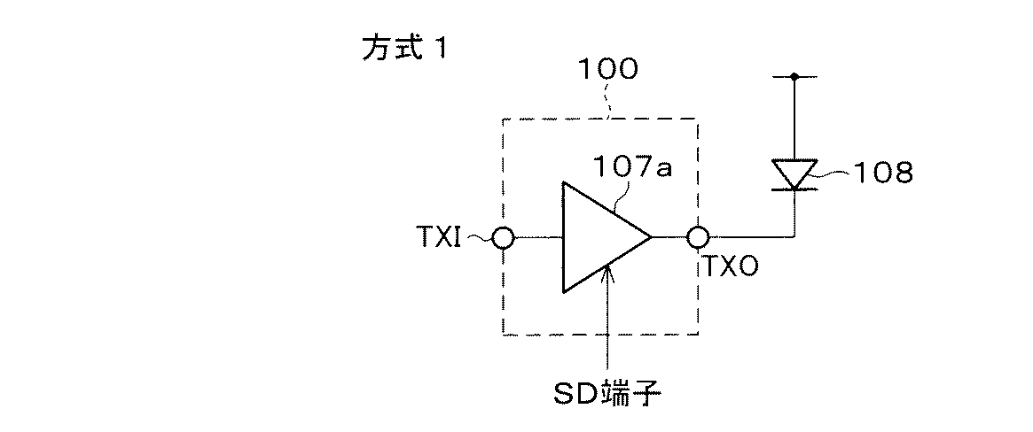
IrDA赤外線通信用ICは電流ドライバーを内蔵し、入力信号に対応した電流を生成してLED駆動用に出力する。図5にIrDA赤外線通信用IC100の等価回路を示す。受信側は、フォトダイオード101から端子HAINを介してICに入った受信電流信号はプリアンプ102とこれに結合されたアンプ103とで増幅され、コンパレータ104および出力段105を経て出力端子RXへ電圧信号として出力される。送信側はTXI端子からロジック回路106に送信信号が入力され、SD端子からロジック回路106に制御信号が入力される。送信信号はLEDドライバー107に入力され、LEDドライバー107は送信信号に対応した電流を生成する。この電流はTXO端子からIC外部に出力され、アノード側に電源が接続されたLED108を駆動する。
【0003】
このように、IrDA赤外線通信用IC100は、受信と送信との機能を兼ね備えていることで、IrDA間での双方向通信を可能にしている。通信レートは、現在では2.4kbps〜4Mbpsまであり、また送信の光の強度は20cmの送受信を可能にするローパワーと、1mの送受信を可能にするハイパワーとがある。このシステムは、それぞれの送信レートおよび発光強度で相手のIrDAと情報の送受信を行うシステムとなっている。
【0004】
以下では、この送信側に関する説明を行う。図6に、IrDA赤外線通信装置の送信部の等価回路を示す。構成としては、送信の入力端子TXIから電圧波形で特徴付けられる送信信号がLEDドライバー107に入力されると、LEDドライバー107が対応する電流を生成し、送信出力端子TXOから出力し、LED108をドライブするものとなっている。
【0005】
また、図7ないし図11に、ドライブ電流値を複数持つ場合に現在用いられている上記送信部のドライブ方式を示す。
【0006】
図7は方式1の構成を示すものであり、1つの入力端子TXI、1つのLEDドライバー107a、および1つの出力端子TXOを備えている。この方式は、ドライブ電流をSD端子によって切り替え制御する方式である。SD端子は通常、回路動作を停止(シャットダウン)させるのに用いるが、ここではドライブ電流制御端子としても併用する。
【0007】
図8は方式2の構成を示すものであり、1つの入力端子TXI、1つのLEDドライバー107b、および1つの出力端子TXOを備えている。この方式は、ドライブ電流をRM端子によって切り替え制御する方式である。
【0008】
図9は方式3の構成を示すものであり、2つの入力端子TXI101・TXI102、入力端子TXI101に対応した1つのLEDドライバー107c、入力端子TXI102に対応した1つのLEDドライバー107d、および1つの出力端子TXOを備えている。この方式は、入力端子TXI101・TXI102のいずれに入力信号が入力されるかで使用するLEDドライバーが決まり、そのLEDドライバーでドライブ電流を制御する方式である。
【0009】
図10は方式4の構成を示すものであり、1つの入力端子TXI、1つのLEDドライバー107e、および2つの出力端子TXO101・TXO102を備えている。出力端子TXO101にはLED108aが、出力端子TXO102にはLED108bがそれぞれ接続される。この方式は、SD端子に入力するラッチでドライブ電流を制御する方式である。
【0010】
図11は方式5の構成を示すものであり、2つの入力端子TXI101・TXI102、入力端子TXI101に対応した1つのLEDドライバー107f、入力端子TXI102に対応した1つのLEDドライバー107g、LEDドライバー107fに対応した1つの出力端子TXO101、およびLEDドライバー107gに対応した1つの出力端子TXO102を備えている。出力端子TXO101にはLED108aが、出力端子TXO102にはLED108bがそれぞれ接続される。この方式は、SD端子およびRM端子に入力される信号、および入力端子TXI101・TXI102のいずれに入力信号が入力されるかでドライブ電流を決定する方式である。
【0011】
また、特許文献1には、1つの入力端子に入力信号が入力され、通信を阻害する外来光の強度に応じて2つの赤外光発光部のうちの所定の一方だけを用いるか、2つとも用いるかを切り替えることができるようになっている送信部が記載されている。
【0012】
【特許文献1】
特開平10−145296号公報
(公開日:平成10年(1998)5月29日)
【0013】
【発明が解決しようとする課題】
しかしながら、従来の電流ドライバー(上記例ではLEDドライバー)内蔵ICでは、いずれの入力端子に入力された入力信号に対していずれの電流ドライバーによって電流を生成して出力するのかということが決まってしまい、様々なドライブ方式に対応することができない。ドライブ方式は、入力端子および出力端子が幾つあって、それを制御するのにどのような端子をどうするのかということによって決まる。
【0014】
従って、前述の方式1〜3、および5では各入力端子に入力された入力信号に対しては使用する電流ドライバーおよび出力端子が決まってしまい、ドライブ方式が1つであることは明らかである。また、方式4や特許文献1の技術も端子の数から言ってドライブ方式は1つである。方式4や特許文献1の技術においては、1つの入力端子に入力される入力信号に対応した電流を2通りに出力することができるとは言え、どちらの出力を用いるかは独立に制御されるのではなく、制御信号の入力によって、一方の電流出力と他方の電流出力とに対して予め定められた相関関係に従う方法でしか制御を行わないようになっている。
【0015】
従って、従来は、電流ドライバー内蔵ICにおいていずれのドライブ方式を取るかは設計時に決定するようになっていることから、ICチップが完成してから複数のドライブ方式が要求されても、その要望に対応することはできなかった。
【0016】
このように、従来では、電流ドライバー内蔵ICのドライブ方式に自由度がないという問題があった。
【0017】
本発明は、上記従来の問題点に鑑みなされたものであり、その目的は、ドライブ方式の自由度が高い電流ドライバー内蔵ICを提供することにある。
【0018】
【課題を解決するための手段】
本発明の電流ドライバー内蔵ICは、上記課題を解決するために、入力端子に入力される入力信号に対応した電流を電流ドライバーによって生成して所定の出力端子から出力する電流ドライバー内蔵ICにおいて、1つもしくは複数の上記入力端子と、複数の上記電流ドライバーと、複数の上記出力端子と、各上記入力端子に入力される上記入力信号に対していずれの上記電流ドライバーで電流を生成するかという組み合わせのうち所定のものを他の上記組み合わせとは独立に選択する選択手段とを備えていることを特徴としている。
【0019】
上記の発明によれば、1つもしくは複数の入力端子のそれぞれに対して、入力信号が入力されるとそれに対応した電流を電流ドライバーで生成するが、選択手段は、入力信号と電流ドライバーとの組み合わせのうち所定のものについては、他の組み合わせとは独立に選択する。選択された電流ドライバーが生成した電流は所定の出力端子から出力される。
【0020】
このように、入力端子と電流ドライバーとの組み合わせの選択を、ある程度独立して行うことにより、完成したICの状態で、各入力端子に入力された入力信号に対応した電流をいずれの電流ドライバーによって生成するかということがそれだけ自由に決められるようになる。従って、それだけ多くのドライブ方式に対応することができる。この結果、ドライブ方式の自由度が高い電流ドライバー内蔵ICを提供することができる。
【0021】
さらに本発明の電流ドライバー内蔵ICは、上記課題を解決するために、上記電流ドライバーを2つ備えていることを特徴としている。
【0022】
上記の発明によれば、ドライブ電流の生成の仕方を2通りに切り替えることができるように要望する場合に、2つの電流ドライバーのそれぞれを切り替えて電流を生成するだけで対応することができる。
【0023】
さらに本発明の電流ドライバー内蔵ICは、上記課題を解決するために、上記入力信号に対して上記電流ドライバーが生成する電流はON値とOFF値との2値からなり、上記電流ドライバーの一方は、上記ON値を複数通り生成することが可能であることを特徴としている。
【0024】
上記の発明によれば、電流ドライバーの生成する電流がON値とOFF値との2値からなる場合に、2つある電流ドライバーの内の1つはそのON値を複数通りに設定することができる。
【0025】
さらに本発明の電流ドライバー内蔵ICは、上記課題を解決するために、上記選択手段に上記電流ドライバーを選択する指示を与える制御信号が入力される制御端子を備えていることを特徴としている。
【0026】
上記の発明によれば、ICの外部から制御端子に電流ドライバーの選択の指示を与える制御信号を入力することができる。
【0027】
さらに本発明の電流ドライバー内蔵ICは、上記課題を解決するために、上記制御端子を複数備えるとともに各上記制御端子には2値の上記制御信号が入力され、上記入力端子を1つもしくは2つ備えるとともに各上記入力端子には2値の上記入力信号が入力され、上記制御端子に入力される上記制御信号と上記入力端子に入力される上記入力信号とからなる真理値表に基づいて、上記選択手段による上記電流ドライバーの選択を含めて上記出力端子からの電流の出力方式を、予め定められた出力方式の中から選択することを特徴としている。
【0028】
上記の発明によれば、1つもしくは2つの入力端子と複数の制御端子とに、真理値表の通りに2値の入力信号および2値の制御信号を入力することによって、電流ドライバーの選択を含めた出力端子からの電流の多数の出力方式を実現することができる。
【0029】
さらに本発明の電流ドライバー内蔵ICは、上記課題を解決するために、上記制御端子を2つ備えていることを特徴としている。
【0030】
上記の発明によれば、2つの制御端子に制御信号を入力することによって電流値を制御したい場合に対応することができる。
【0031】
さらに本発明の電流ドライバー内蔵ICは、上記課題を解決するために、上記電流ドライバーをIrDA方式のLED駆動用に用いることを特徴としている。
【0032】
上記の発明によれば、IrDA用の1チップの電流ドライバー内蔵ICにおいて複数のドライブ方式を選択することができる。
【0033】
さらに本発明の電流ドライバー内蔵ICは、上記課題を解決するために、上記入力信号は1種類であることを特徴としている。
【0034】
上記の発明によれば、1種類の入力信号に対して、様々なドライブ方式を実現することができる。
【0035】
【発明の実施の形態】
本発明の実施の形態について図1ないし図4に基づいて説明すれば以下の通りである。
【0036】
図1に、本実施の形態に係る電流ドライバー内蔵IC1の構成を示す。電流ドライバー内蔵IC1は例えばIrDA方式の通信に使用されるICであり、入力端子TXI1・TXI2・TXI3・…、ドライブ電流値制御ブロック2、LEDドライバー3・4・5・…、および出力端子TXO1・TXO2・TXO3・…を備えている。なお、ここでは入力端子、LEDドライバー、および出力端子がそれぞれ3つの場合を説明するが、一般には複数でよい。また、入力端子は1つでもよい。さらに、入力端子、LEDドライバー、および出力端子は互いに同数でなくてもよい。
【0037】
入力端子TXI1・TXI2・TXI3のそれぞれに対して2値の入力信号が入力されると、入力信号はドライブ電流値制御ブロック2に入力される。ドライブ電流値制御ブロック(選択手段)2は、各入力端子TXI1・TXI2・TXI3に入力される入力信号に対していずれのLEDドライバーによって電流を生成するかという組み合わせを他の組み合わせとは独立に選択する。例えば、入力端子TXI1に入力された入力信号に対してLEDドライバー3で電流を生成するのと、入力端子TXI1に入力された入力信号に対してLEDドライバー4で電流を生成するのとを独立に選択する。あるいはまた、入力端子TXI2に入力された入力信号に対してLEDドライバー4で電流を生成するのと、入力端子TXI3に入力された入力信号に対してLEDドライバー5で電流を生成するのとを独立に選択する。すなわち、これらの選択では、一方の選択結果が他方の選択条件に依存しない。
【0038】
また、これらの組み合わせの全てを独立に選択するのには限られず、全ての組み合わせのうち所定のものが他の組み合わせに対して独立に選択されるようになっていればよい。さらに、入力端子TXI1・TXI2・TXI3のいずれか1つにのみ入力信号が入力されるのか、複数の入力端子に同時に入力信号が入力されるのかといったことも問わない。
【0039】
LEDドライバー(電流ドライバー)3・4・5は、ここではON値とOFF値との2値からなる電流を生成する。LEDドライバー3は出力端子TXO1に、LEDドライバー4は出力端子TXO2に、LEDドライバー5は出力端子TXO3に、それぞれ電流を出力する。出力端子TXO1・TXO2・TXO3には、順にLED6・7・8が接続され、電流が出力された出力端子に接続されたLEDが光信号を送信する。
【0040】
上述した構成の原則に従って、例えばICに2個の入力端子および2個の出力端子を備え、入力端子とLEDドライバーとの組み合わせ制御が数種類できれば、製品としてのICの使用方法にはそれだけの自由度がもてる。従って、複数の使用方法を要望するユーザー(その製品を使う人)に対して1つのICチップで全て対応できる製品を作ることも可能になる。回路設計時に将来的にどのドライブ方式を採用するか決定されていない場合、またはICチップ完成後に同時に複数のドライブ方式が要求された場合のいずれの要求にも対応可能となる。これにより、1つのICチップを開発しておけば、使用する上で、入力端子や出力端子を1個とするか2個とするかといったことや、その制御方法も複数通り選べるようになる。
【0041】
このように、入力端子TXI1・TXI2・TXI3とLEDドライバー3・4・5との組み合わせの選択を、ある程度独立して行うことにより、完成したICの状態で、各入力端子に入力された入力信号に対応した電流をいずれの電流ドライバーによって生成するかということがそれだけ自由に決められるようになる。従って、それだけ多くのドライブ方式に対応することができる。このように、電流ドライバー内蔵IC1は、ドライブ方式の自由度が高い電流ドライバー内蔵ICである。
【0042】
次に、図2に、別の電流ドライバー内蔵IC11の構成を示す。電流ドライバー内蔵IC11は、入力端子TXI11・TXI12、SD端子P1、RM端子P2、ドライブ電流値制御ブロック12、LEDドライバー(電流ドライバー)13・14、および出力端子TXO11・TXO12を備えている。LEDドライバー(電流ドライバー)13・14に対して順に、出力端子TXO11・TXO12が接続され、それぞれLED15、LED16へ電流を出力する。
【0043】
電流ドライバー内蔵IC11は、前記電流ドライバー内蔵IC1の入力端子、LEDドライバー、および出力端子をそれぞれ2つとし、ドライブ電流値制御ブロック(選択手段)12がどのLEDドライバーによって電流を生成するのかを、SD端子P1およびRM端子P2という制御端子に制御信号を入力して指示するようにしたものである。SD端子P1は、回路をシャットダウンする時に用いるSD端子を上記制御信号が入力される端子として併用したものであり、RM端子P2はドライブ電流制御専用の端子である。
【0044】
これにより、ICの外部からSD端子P1およびRM端子P2にLEDドライバー13・14の選択の指示を与えることができる。
【0045】
また、LEDドライバーを2つ備えているので、例えばON値を2通りに切り替えるといったようにドライブ電流の生成の仕方を2通りに切り替えることができるように要望する場合に、2つのLEDドライバー13・14のそれぞれを切り替えて電流を生成するだけで対応することができる。
【0046】
次に、図3に、上記電流ドライバー内蔵IC11におけるドライブ電流値制御ブロック12の構成をスイッチで擬似的に示す。
【0047】
ドライブ電流値制御ブロック12は、スイッチSW1・SW2を備えている。スイッチSW1は入力端子aおよび出力端子b1・b2を備えており、SD端子P1およびRM端子P2に入力される制御信号に応じて、入力端子aを出力端子b1あるいはb2に切り替え接続する。スイッチSW2は入力端子cおよび出力端子d1・d2を備えており、SD端子P1およびRM端子P2に入力される制御信号に応じて、入力端子cを出力端子d1あるいはd2に切り替え接続する。スイッチSW1の出力端子b1はLEDドライバー13の入力端子に、スイッチSW1の出力端子b2はLEDドライバー14の入力端子に、スイッチSW2の出力端子d1はLEDドライバー13の入力端子に、スイッチSW2の出力端子d2はLEDドライバー14の入力端子に、それぞれ接続されている。
【0048】
これにより、入力端子TXI11・TXI12のそれぞれを、LEDドライバー13・14のそれぞれに接続することができる。この接続関係は、SD端子P1およびRM端子P2に入力される制御信号によって決定される。
【0049】
次に、図4に、図3のドライブ電流値制御ブロック12を論理回路で表現した場合の構成を示す。なお、この構成には、LEDドライバー14の電流値を切り替える電流値制御回路21が追加されている。上記論理回路は、ORゲート31・39、ANDゲート32・33・34・35・36・37・38、およびインバータ40・41・42を備えている。ORゲートおよびANDゲートは全て2入力である。
【0050】
ORゲート31の入力端子はSD端子P1およびRM端子P2に接続されている。ANDゲート32の入力端子は入力端子TXI1・TXI2に接続されている。ANDゲート33の入力端子はANDゲート32の出力端子およびインバータ42の出力端子に接続されている。ANDゲート34の入力端子は入力端子TXI1およびインバータ40の出力端子に接続されている。ANDゲート35の入力端子はインバータ41の出力端子および入力端子TXI2に接続されている。ANDゲート36の入力端子はANDゲート34の出力端子およびインバータ42の出力端子に接続されている。
【0051】
ANDゲート37の入力端子はORゲート31の出力端子およびANDゲート32の出力端子に接続されている。ANDゲート38の入力端子はANDゲート33の出力端子およびANDゲート36の出力端子に接続されている。ORゲート39の入力端子はANDゲート35の出力端子およびANDゲート37の出力端子に接続されている。インバータ40の入力端子は入力端子TXI2に接続されている。インバータ41の入力端子は入力端子TXI1に接続されている。インバータ42の入力端子はORゲート31の出力端子に接続されている。
【0052】
ANDゲート38の出力端子はLEDドライバー13の入力端子に接続されている。ORゲート39の出力端子はLEDドライバー14の入力端子に接続されている。
【0053】
また、電流値制御回路21は、入力端子TX1・TX2、SD端子P1、RM端子P2をそれぞれ入力端子とする。そして、入力端子TX1・TX2に入力された入力信号、SD端子P1およびRM端子P2に入力された制御信号を基に、LEDドライバー14の電流のON値を複数通りに切り替えるようになっている。LEDドライバー13とLEDドライバー14とは、ここでは電流のON値に大小2通り(一方が大で他方が小)を設けるために備えられている。
【0054】
そしてここでは、SD端子P1およびRM端子P2に入力される制御信号と、入力端子TXI1・TXI2に入力される入力信号とからなる真理値表に基づいて、ドライブ電流値制御ブロック12によるLEDドライバー13・14の選択と、LEDドライバー14の電流値をどのように設定するかということとを含む電流の出力方式を、予め定められた出力方式の中から選択するようになっている。表1に、入力端子が2つの場合の上記真理値表を示す。
【0055】
【表1】
前記予め定められた出力方式のそれぞれは、表1に記載したドライブ方式およびモードのそれぞれに対応している。そして、各ドライブ方式およびモードにおける出力端子TXO1・TXO2の出力電流の値(ON値)をI1〜I8で示してある。この場合、LEDドライバー14のON値はI2〜I8の7通りに設定される。
【0057】
既出の図7〜図11に示した、現在考えられる5通りの電流ドライブ方式については、
方式1および4は真理値表のドライブ方式1▲1▼および1▲2▼で、
方式2は真理値表のドライブ方式2▲1▼および2▲2▼で、
方式3および5は真理値表のドライブ方式3▲1▼および3▲2▼で、
それぞれ実現することができる。
【0058】
このように2つの送信信号入力端子、2つの送信電流出力端子、および2つの制御端子を備えているので、上記の真理値表に従い出力電流値を決定するようにしておけば、現在考えうる5通りの電流ドライブ方式全てに対応することができる。また、上記真理値表によれば、A〜Fと記載されているように前記5通りを越えるドライブ方式を選択することが可能であり、LEDドライバー13・14の選択を含めた出力端子TXO1・TXO2からの電流の多数の出力方式を実現することができるのが分かる。
【0059】
また、1つの送信信号入力端子、2つの送信電流出力端子、および2つの制御端子を備える場合、方式1,2,4の3通りの電流ドライブ方式に対応することができる。前記例では入力信号が2種類であったが、この場合の入力信号は1種類である。また、入力端子の数に関わらず、入力信号は1種類であってもよい。1種類の入力信号に対しても、様々なドライブ方式を実現することができる。
【0060】
【発明の効果】
本発明の電流ドライバー内蔵ICは、以上のように、1つもしくは複数の上記入力端子と、複数の上記電流ドライバーと、複数の上記出力端子と、各上記入力端子に入力される上記入力信号に対していずれの上記電流ドライバーで電流を生成するかという組み合わせのうち所定のものを他の上記組み合わせとは独立に選択する選択手段とを備えている構成である。
【0061】
それゆえ、完成したICの状態で、各入力端子に入力された入力信号に対応した電流をいずれの電流ドライバーによって生成するかということがそれだけ自由に決められるようになる。従って、それだけ多くのドライブ方式に対応することができる。この結果、ドライブ方式の自由度が高い電流ドライバー内蔵ICを提供することができるという効果を奏する。
【0062】
さらに本発明の電流ドライバー内蔵ICは、以上のように、上記電流ドライバーを2つ備えている構成である。
【0063】
それゆえ、ドライブ電流の生成の仕方を2通りに切り替えることができるように要望する場合に、2つの電流ドライバーのそれぞれを切り替えて電流を生成するだけで対応することができるという効果を奏する。
【0064】
さらに本発明の電流ドライバー内蔵ICは、以上のように、上記入力信号に対して上記電流ドライバーが生成する電流はON値とOFF値との2値からなり、上記電流ドライバーの一方は、上記ON値を複数通り生成することが可能である構成である。
【0065】
それゆえ、電流ドライバーの生成する電流がON値とOFF値との2値からなる場合に、2つある電流ドライバーの内の1つはそのON値を複数通りに設定することができるという効果を奏する。
【0066】
さらに本発明の電流ドライバー内蔵ICは、以上のように、上記選択手段に上記電流ドライバーを選択する指示を与える制御信号が入力される制御端子を備えている構成である。
【0067】
それゆえ、ICの外部から制御端子に電流ドライバーの選択の指示を与える制御信号を入力することができるという効果を奏する。
【0068】
さらに本発明の電流ドライバー内蔵ICは、以上のように、上記制御端子を複数備えるとともに各上記制御端子には2値の上記制御信号が入力され、上記入力端子を1つもしくは2つ備えるとともに各上記入力端子には2値の上記入力信号が入力され、上記制御端子に入力される上記制御信号と上記入力端子に入力される上記入力信号とからなる真理値表に基づいて、上記選択手段による上記電流ドライバーの選択を含めて上記出力端子からの電流の出力方式を、予め定められた出力方式の中から選択する構成である。
【0069】
それゆえ、入力端子と制御端子とに、真理値表の通りに2値の入力信号および2値の制御信号を入力することによって、電流ドライバーの選択を含めた出力端子からの電流の多数の出力方式を実現することができるという効果を奏する。
【0070】
さらに本発明の電流ドライバー内蔵ICは、以上のように、上記制御端子を2つ備えている構成である。
【0071】
それゆえ、2つの制御端子に制御信号を入力することによって電流値を制御したい場合に対応することができるという効果を奏する。
【0072】
さらに本発明の電流ドライバー内蔵ICは、以上のように、上記電流ドライバーをIrDA方式のLED駆動用に用いる構成である。
【0073】
それゆえ、IrDA用の1チップの電流ドライバー内蔵ICにおいて複数のドライブ方式を選択することができるという効果を奏する。
【0074】
さらに本発明の電流ドライバー内蔵ICは、以上のように、上記入力信号は1種類である構成である。
【0075】
それゆえ、1種類の入力信号に対して、様々なドライブ方式を実現することができるという効果を奏する。
【図面の簡単な説明】
【図1】本発明の実施の形態に係る第1の電流ドライバー内蔵ICの構成を示す回路ブロック図である。
【図2】本発明の実施の形態に係る第2の電流ドライバー内蔵ICの構成を示す回路ブロック図である。
【図3】図2の電流ドライバー内蔵ICのドライブ電流値制御ブロックをスイッチで表現した場合の構成を示す回路ブロック図である。
【図4】図3の電流ドライバー内蔵ICのドライブ電流値制御ブロックを論値回路で表現した場合の構成を示す回路ブロック図である。
【図5】従来の電流ドライバー内蔵ICの構成を示す回路ブロック図である。
【図6】IrDA赤外線通信装置の送信部の構成を示す回路ブロック図である。
【図7】従来の電流ドライバー内蔵ICの第1の電流ドライブ方式を説明するための回路ブロック図である。
【図8】従来の電流ドライバー内蔵ICの第2の電流ドライブ方式を説明するための回路ブロック図である。
【図9】従来の電流ドライバー内蔵ICの第3の電流ドライブ方式を説明するための回路ブロック図である。
【図10】従来の電流ドライバー内蔵ICの第4の電流ドライブ方式を説明するための回路ブロック図である。
【図11】従来の電流ドライバー内蔵ICの第5の電流ドライブ方式を説明するための回路ブロック図である。
【符号の説明】
1 電流ドライバー内蔵IC
2 ドライブ電流値制御ブロック(選択手段)
3〜5 LEDドライバー(電流ドライバー)
11 電流ドライバー内蔵IC
12 ドライブ電流値制御ブロック(選択手段)
13,14 LEDドライバー(電流ドライバー)
TXI1〜TXI3
入力端子
TXO1〜TXO3
出力端子
TXI11,TXI12
入力端子
TXO11,TXO12
出力端子
P1 SD端子(制御端子)
P2 RM端子(制御端子)[0001]
BACKGROUND OF THE INVENTION
The present invention relates to a current driver built-in IC that generates and outputs a current corresponding to an input signal by a current driver.
[0002]
[Prior art]
The IrDA infrared communication IC incorporates a current driver, generates a current corresponding to the input signal, and outputs the current for driving the LED. FIG. 5 shows an equivalent circuit of the IrDA
[0003]
As described above, the IrDA
[0004]
Hereinafter, the transmission side will be described. FIG. 6 shows an equivalent circuit of the transmission unit of the IrDA infrared communication device. As a configuration, when a transmission signal characterized by a voltage waveform is input to the
[0005]
FIGS. 7 to 11 show the drive method of the transmission unit currently used when there are a plurality of drive current values.
[0006]
FIG. 7 shows a configuration of
[0007]
FIG. 8 shows the configuration of
[0008]
FIG. 9 shows the configuration of
[0009]
FIG. 10 shows the configuration of system 4, which includes one input terminal TXI, one
[0010]
FIG. 11 shows the configuration of
[0011]
In
[0012]
[Patent Document 1]
Japanese Patent Laid-Open No. 10-145296
(Release date: May 29, 1998)
[0013]
[Problems to be solved by the invention]
However, in a conventional IC with a built-in current driver (LED driver in the above example), it is determined which current driver generates and outputs a current with respect to an input signal input to which input terminal. It cannot support various drive systems. The drive system is determined by the number of input terminals and output terminals, and what kind of terminals are used to control them.
[0014]
Therefore, in the above-described
[0015]
Therefore, in the past, it has been decided at the time of designing which drive system to use in an IC with a built-in current driver. Therefore, even if a plurality of drive systems are required after the IC chip is completed, the demand is met. I couldn't respond.
[0016]
As described above, conventionally, there is a problem that the drive system of the IC with a built-in current driver is not flexible.
[0017]
The present invention has been made in view of the above-described conventional problems, and an object thereof is to provide an IC with a built-in current driver that has a high degree of freedom in a drive system.
[0018]
[Means for Solving the Problems]
In order to solve the above problems, an IC with a built-in current driver according to the present invention is an IC with a built-in current driver that generates a current corresponding to an input signal input to an input terminal by a current driver and outputs the current from a predetermined output terminal. A combination of one or a plurality of the input terminals, a plurality of the current drivers, a plurality of the output terminals, and which of the current drivers generates the current for the input signal input to each of the input terminals. Selection means for selecting a predetermined one of them independently of the other combinations described above.
[0019]
According to the above invention, when an input signal is input to each of one or a plurality of input terminals, a current corresponding to the input signal is generated by the current driver. The predetermined combinations are selected independently from the other combinations. The current generated by the selected current driver is output from a predetermined output terminal.
[0020]
In this way, by selecting the combination of the input terminal and the current driver to some extent independently, the current corresponding to the input signal input to each input terminal can be obtained by any current driver in the completed IC state. Whether to generate it can be decided freely. Therefore, it is possible to cope with many drive systems. As a result, it is possible to provide an IC with a built-in current driver that has a high degree of freedom in the drive system.
[0021]
Furthermore, the IC with a built-in current driver according to the present invention is characterized in that two current drivers are provided in order to solve the above problems.
[0022]
According to the above-described invention, when it is desired that the method of generating the drive current can be switched in two ways, it is possible to cope with it by simply switching each of the two current drivers to generate a current.
[0023]
Further, in order to solve the above problems, the current driver built-in IC according to the present invention has a current generated by the current driver with respect to the input signal, which is a binary value of an ON value and an OFF value. A plurality of ON values can be generated.
[0024]
According to the above invention, when the current generated by the current driver is composed of two values of the ON value and the OFF value, one of the two current drivers can set the ON value in a plurality of ways. it can.
[0025]
Furthermore, in order to solve the above-mentioned problem, the IC with a built-in current driver according to the present invention is characterized by including a control terminal to which a control signal for giving an instruction to select the current driver is input to the selection means.
[0026]
According to the above invention, it is possible to input a control signal for giving an instruction to select a current driver to the control terminal from the outside of the IC.
[0027]
Furthermore, in order to solve the above problems, the IC with a built-in current driver of the present invention includes a plurality of the control terminals, and the binary control signal is input to each control terminal, and one or two input terminals are provided. And each of the input terminals is supplied with the binary input signal, and based on a truth table composed of the control signal input to the control terminal and the input signal input to the input terminal. A method for outputting a current from the output terminal including selection of the current driver by a selection unit is selected from predetermined output methods.
[0028]
According to the above invention, the current driver can be selected by inputting a binary input signal and a binary control signal to one or two input terminals and a plurality of control terminals as shown in the truth table. Many output methods of current from the included output terminals can be realized.
[0029]
Furthermore, the IC with a built-in current driver according to the present invention is characterized in that it has two control terminals in order to solve the above problems.
[0030]
According to said invention, it can respond to the case where it is desired to control the current value by inputting control signals to the two control terminals.
[0031]
Furthermore, the IC with a built-in current driver according to the present invention is characterized in that the current driver is used for driving an IrDA type LED in order to solve the above-mentioned problems.
[0032]
According to the above invention, a plurality of drive systems can be selected in a one-chip IC with a current driver for IrDA.
[0033]
Furthermore, in order to solve the above problems, the IC with a built-in current driver according to the present invention is characterized in that the input signal is one kind.
[0034]
According to the above invention, various drive systems can be realized for one type of input signal.
[0035]
DETAILED DESCRIPTION OF THE INVENTION
The embodiment of the present invention will be described below with reference to FIGS.
[0036]
FIG. 1 shows a configuration of an
[0037]
When a binary input signal is input to each of the input terminals TXI1, TXI2, and TXI3, the input signal is input to the drive current
[0038]
Moreover, it is not restricted to selecting all of these combinations independently, and the predetermined thing should just be able to be selected independently with respect to another combination among all the combinations. Furthermore, it does not matter whether an input signal is input to any one of the input terminals TXI1, TXI2, and TXI3, or whether input signals are input to a plurality of input terminals simultaneously.
[0039]
Here, the LED drivers (current drivers) 3, 4, and 5 generate a current composed of two values of an ON value and an OFF value. The
[0040]
If the IC has two input terminals and two output terminals according to the principle of the configuration described above, and the combination control of the input terminal and the LED driver can be performed in several ways, the use of the IC as a product has such flexibility. I can have it. Therefore, it is possible to make a product that can be handled by a single IC chip for users who want a plurality of usage methods (people who use the product). When it is not determined which drive system will be adopted in the future at the time of circuit design, or when a plurality of drive systems are requested at the same time after the completion of the IC chip, it becomes possible to respond to any request. As a result, if one IC chip is developed, it is possible to select a plurality of control methods for determining whether to use one or two input terminals and output terminals in use.
[0041]
In this way, by selecting the combination of the input terminals TXI1, TXI2, TXI3 and the
[0042]
Next, FIG. 2 shows a configuration of another
[0043]
The
[0044]
Thereby, an instruction for selecting the
[0045]
In addition, since two LED drivers are provided, for example, when it is desired to be able to switch the drive current generation method in two ways, such as switching the ON value in two ways, the two
[0046]
Next, FIG. 3 shows a pseudo configuration of the drive current
[0047]
The drive current
[0048]
Accordingly, the input terminals TXI11 and TXI12 can be connected to the
[0049]
Next, FIG. 4 shows a configuration when the drive current
[0050]
The input terminal of the
[0051]
The input terminal of the AND
[0052]
The output terminal of the AND
[0053]
The current
[0054]
And here, based on the truth table which consists of the control signal which is input to SD terminal P1 and RM terminal P2 and the input signal which is input to input terminals TXI1 and TXI2,
[0055]
[Table 1]
Each of the predetermined output methods corresponds to each of the drive methods and modes described in Table 1. The values (ON values) of the output currents of the output terminals TXO1 and TXO2 in the respective drive systems and modes are indicated by I1 to I8. In this case, the ON value of the
[0057]
Regarding the five current drive systems currently considered shown in FIGS. 7 to 11,
Each can be realized.
[0058]
As described above, since the two transmission signal input terminals, the two transmission current output terminals, and the two control terminals are provided, if the output current value is determined according to the above truth table, it can be currently considered. All current drive methods can be supported. Further, according to the truth table, it is possible to select more than the above five drive methods as described in A to F, and output terminals TXO1,. It can be seen that multiple output schemes for current from TXO2 can be realized.
[0059]
Further, when one transmission signal input terminal, two transmission current output terminals, and two control terminals are provided, it is possible to correspond to three types of current drive systems of
[0060]
【The invention's effect】
As described above, the IC with a built-in current driver according to the present invention receives one or a plurality of the input terminals, a plurality of the current drivers, a plurality of the output terminals, and the input signal input to each of the input terminals. On the other hand, it is a structure provided with the selection means which selects the predetermined thing among the combinations of which said current driver produces | generates an electric current independently from the said other said combination.
[0061]
Therefore, in a completed IC state, it can be freely determined by which current driver the current corresponding to the input signal input to each input terminal is generated. Therefore, it is possible to cope with many drive systems. As a result, it is possible to provide an IC with a built-in current driver that has a high degree of freedom in the drive system.
[0062]
Furthermore, the current driver built-in IC of the present invention has a configuration including two current drivers as described above.
[0063]
Therefore, when it is desired that the method of generating the drive current can be switched in two ways, it is possible to cope with this by simply switching each of the two current drivers to generate a current.
[0064]
In the current driver built-in IC according to the present invention, as described above, the current generated by the current driver with respect to the input signal is composed of two values, an ON value and an OFF value. In this configuration, a plurality of values can be generated.
[0065]
Therefore, when the current generated by the current driver consists of two values, an ON value and an OFF value, one of the two current drivers can set the ON value in multiple ways. Play.
[0066]
Furthermore, the IC with a built-in current driver according to the present invention is configured to include a control terminal to which a control signal for giving an instruction to select the current driver is input to the selection means.
[0067]
Therefore, it is possible to input a control signal for giving an instruction to select a current driver to the control terminal from the outside of the IC.
[0068]
Furthermore, as described above, the IC with a built-in current driver according to the present invention includes a plurality of the control terminals, and the control signals of binary values are input to the control terminals, and each of the input terminals includes one or two input terminals. The binary input signal is input to the input terminal, and based on a truth table composed of the control signal input to the control terminal and the input signal input to the input terminal, In this configuration, the current output method from the output terminal including selection of the current driver is selected from predetermined output methods.
[0069]
Therefore, by inputting a binary input signal and a binary control signal to the input terminal and the control terminal as shown in the truth table, a large number of outputs of current from the output terminal including the selection of the current driver can be obtained. There is an effect that the method can be realized.
[0070]
Furthermore, the current driver built-in IC according to the present invention is configured to include the two control terminals as described above.
[0071]
Therefore, there is an effect that it is possible to cope with the case where it is desired to control the current value by inputting control signals to the two control terminals.
[0072]
Furthermore, the current driver built-in IC of the present invention is configured to use the current driver for driving an IrDA type LED as described above.
[0073]
Therefore, there is an effect that a plurality of drive systems can be selected in a one-chip current driver IC for IrDA.
[0074]
Furthermore, the current driver built-in IC of the present invention has a configuration in which the input signal is one kind as described above.
[0075]
Therefore, there is an effect that various drive methods can be realized for one type of input signal.
[Brief description of the drawings]
FIG. 1 is a circuit block diagram showing a configuration of a first current driver built-in IC according to an embodiment of the present invention;
FIG. 2 is a circuit block diagram showing a configuration of a second current driver built-in IC according to the embodiment of the present invention;
3 is a circuit block diagram showing a configuration when a drive current value control block of the IC with a built-in current driver in FIG. 2 is expressed by a switch.
4 is a circuit block diagram showing a configuration when a drive current value control block of the IC with a built-in current driver in FIG. 3 is expressed by a logic circuit.
FIG. 5 is a circuit block diagram showing a configuration of a conventional IC with a built-in current driver.
FIG. 6 is a circuit block diagram illustrating a configuration of a transmission unit of an IrDA infrared communication device.
FIG. 7 is a circuit block diagram for explaining a first current drive method of a conventional IC with a built-in current driver.
FIG. 8 is a circuit block diagram for explaining a second current driving method of a conventional IC with a built-in current driver.
FIG. 9 is a circuit block diagram for explaining a third current driving method of a conventional IC with a built-in current driver.
FIG. 10 is a circuit block diagram for explaining a fourth current drive method of a conventional IC with a built-in current driver.
FIG. 11 is a circuit block diagram for explaining a fifth current drive method of a conventional IC with a built-in current driver.
[Explanation of symbols]
1 IC with built-in current driver
2 Drive current value control block (selection means)
3-5 LED driver (current driver)
11 IC with built-in current driver
12 Drive current value control block (selection means)
13, 14 LED driver (current driver)
TXI1 to TXI3
Input terminal
TXO1-TXO3
Output terminal
TXI11, TXI12
Input terminal
TXO11, TXO12
Output terminal
P1 SD terminal (control terminal)
P2 RM terminal (control terminal)
Claims (8)
1つもしくは複数の上記入力端子と、複数の上記電流ドライバーと、複数の上記出力端子と、各上記入力端子に入力される上記入力信号に対していずれの上記電流ドライバーで電流を生成するかという組み合わせのうち所定のものを他の上記組み合わせとは独立に選択する選択手段とを備えており、
上記電流ドライバーを2つ備えており、
上記入力信号に対して上記電流ドライバーが生成する電流はON値とOFF値との2値からなり、上記電流ドライバーの一方は、上記ON値を複数通り生成することが可能であることを特徴とする電流ドライバー内蔵IC。In a current driver built-in IC that generates a current corresponding to an input signal input to an input terminal by a current driver and outputs the current from a predetermined output terminal.
One or a plurality of the input terminals, a plurality of the current drivers, a plurality of the output terminals, and which of the current drivers generates a current for the input signal input to each of the input terminals. Selection means for selecting a predetermined one of the combinations independently of the other combinations described above ,
Two current drivers are provided,
Current the current driver generates for the input signal consists of two values of ON value and the OFF value, one of the current drivers, wherein can der Rukoto generating plural kinds of the ON value IC with a built-in current driver.
上記入力端子を1つもしくは2つ備えるとともに各上記入力端子には2値の上記入力信号が入力され、
上記制御端子に入力される上記制御信号と上記入力端子に入力される上記入力信号とからなる真理値表に基づいて、上記選択手段による上記電流ドライバーの選択を含めて上記出力端子からの電流の出力方式を、予め定められた出力方式の中から選択することを特徴とする請求項2に記載の電流ドライバー内蔵IC。A plurality of the control terminals and a binary control signal are input to each control terminal,
One or two input terminals are provided, and the binary input signal is input to each input terminal.
Based on the truth table composed of the control signal input to the control terminal and the input signal input to the input terminal, the current from the output terminal is selected including the selection of the current driver by the selection means. current driver incorporated IC according to claim 2 the output method, characterized by you to select from among the output format determined in advance.
1つもしくは複数の上記入力端子と、複数の上記電流ドライバーと、複数の上記出力端子と、各上記入力端子に入力される上記入力信号に対していずれの上記電流ドライバーで電流を生成するかという組み合わせのうち所定のものを他の上記組み合わせとは独立に選択する選択手段とを備えており、
上記選択手段に上記電流ドライバーを選択する指示を与える制御信号が入力される制御端子を備えており、
上記制御端子を複数備えるとともに各上記制御端子には2値の上記制御信号が入力され、
上記入力端子を1つもしくは2つ備えるとともに各上記入力端子には2値の上記入力信号が入力され、
上記制御端子に入力される上記制御信号と上記入力端子に入力される上記入力信号とからなる真理値表に基づいて、上記選択手段による上記電流ドライバーの選択を含めて上記出力端子からの電流の出力方式を、予め定められた出力方式の中から選択することを特徴とする電流ドライバー内蔵IC。 In a current driver built-in IC that generates a current corresponding to an input signal input to an input terminal by a current driver and outputs the current from a predetermined output terminal.
One or a plurality of the input terminals, a plurality of the current drivers, a plurality of the output terminals, and which of the current drivers generates a current for the input signal input to each of the input terminals. Selection means for selecting a predetermined one of the combinations independently of the other combinations described above,
A control terminal for inputting a control signal for giving an instruction to select the current driver to the selection means;
A plurality of the control terminals and a binary control signal are input to each control terminal,
One or two input terminals are provided, and the binary input signal is input to each input terminal.
Based on the truth table composed of the control signal input to the control terminal and the input signal input to the input terminal, the current from the output terminal is selected including the selection of the current driver by the selection means. An IC with a built- in current driver, wherein an output method is selected from predetermined output methods .
Priority Applications (1)
| Application Number | Priority Date | Filing Date | Title |
|---|---|---|---|
| JP2002359884A JP4101630B2 (en) | 2002-12-11 | 2002-12-11 | IC with built-in current driver |
Applications Claiming Priority (1)
| Application Number | Priority Date | Filing Date | Title |
|---|---|---|---|
| JP2002359884A JP4101630B2 (en) | 2002-12-11 | 2002-12-11 | IC with built-in current driver |
Publications (2)
| Publication Number | Publication Date |
|---|---|
| JP2004193361A JP2004193361A (en) | 2004-07-08 |
| JP4101630B2 true JP4101630B2 (en) | 2008-06-18 |
Family
ID=32759149
Family Applications (1)
| Application Number | Title | Priority Date | Filing Date |
|---|---|---|---|
| JP2002359884A Expired - Fee Related JP4101630B2 (en) | 2002-12-11 | 2002-12-11 | IC with built-in current driver |
Country Status (1)
| Country | Link |
|---|---|
| JP (1) | JP4101630B2 (en) |
-
2002
- 2002-12-11 JP JP2002359884A patent/JP4101630B2/en not_active Expired - Fee Related
Also Published As
| Publication number | Publication date |
|---|---|
| JP2004193361A (en) | 2004-07-08 |
Similar Documents
| Publication | Publication Date | Title |
|---|---|---|
| TWI325130B (en) | Led current driving system for lcos display | |
| JP2004533111A5 (en) | ||
| JP2005346123A (en) | Storage device equipped with parallel interface connector and conversion connector applied to same device | |
| US6950610B2 (en) | Optical communication interface module for universal serial bus | |
| EP3928710A1 (en) | Ultrasound imaging apparatus | |
| JP4101630B2 (en) | IC with built-in current driver | |
| JPH05158429A (en) | Information transmission circuit | |
| JP4029319B2 (en) | Lighting control system and signal converter | |
| JPH06338778A (en) | Bidirectional optical coupler | |
| US10306716B1 (en) | Control signal switching system | |
| JP4164544B2 (en) | CAMERA SUPPORT DEVICE WITH MULTIFUNCTIONAL ASSEMBLY Worn on the Body and Consisting of Multiple Electric Elements | |
| JP3945308B2 (en) | Optical transmitter | |
| JP6021387B2 (en) | Video display device | |
| KR102663136B1 (en) | ultrasonic imaging device | |
| JP2007278561A (en) | Communication device | |
| JP3724271B2 (en) | Optical signal transmission device and optical signal generation device | |
| JP2018142100A (en) | Control device | |
| JP2003204301A (en) | Optical switch control signal transmitter and optical switch controller | |
| JP4991044B2 (en) | Module control panel for video equipment | |
| JP3971620B2 (en) | Communication apparatus and communication system | |
| JP2003348887A (en) | Test system for motor driver | |
| US5466944A (en) | Optically-coupled differential line receiver | |
| CN113346344A (en) | Signal control device and method and laser equipment | |
| JPH079468Y2 (en) | Signal input device | |
| JP3136020B2 (en) | Multiplex communication method |
Legal Events
| Date | Code | Title | Description |
|---|---|---|---|
| A621 | Written request for application examination |
Free format text: JAPANESE INTERMEDIATE CODE: A621 Effective date: 20050525 |
|
| A977 | Report on retrieval |
Free format text: JAPANESE INTERMEDIATE CODE: A971007 Effective date: 20071217 |
|
| A131 | Notification of reasons for refusal |
Free format text: JAPANESE INTERMEDIATE CODE: A131 Effective date: 20071225 |
|
| A521 | Written amendment |
Free format text: JAPANESE INTERMEDIATE CODE: A523 Effective date: 20080225 |
|
| RD02 | Notification of acceptance of power of attorney |
Free format text: JAPANESE INTERMEDIATE CODE: A7422 Effective date: 20080225 |
|
| TRDD | Decision of grant or rejection written | ||
| A01 | Written decision to grant a patent or to grant a registration (utility model) |
Free format text: JAPANESE INTERMEDIATE CODE: A01 Effective date: 20080318 |
|
| A61 | First payment of annual fees (during grant procedure) |
Free format text: JAPANESE INTERMEDIATE CODE: A61 Effective date: 20080319 |
|
| FPAY | Renewal fee payment (event date is renewal date of database) |
Free format text: PAYMENT UNTIL: 20110328 Year of fee payment: 3 |
|
| R150 | Certificate of patent or registration of utility model |
Free format text: JAPANESE INTERMEDIATE CODE: R150 |
|
| FPAY | Renewal fee payment (event date is renewal date of database) |
Free format text: PAYMENT UNTIL: 20120328 Year of fee payment: 4 |
|
| FPAY | Renewal fee payment (event date is renewal date of database) |
Free format text: PAYMENT UNTIL: 20120328 Year of fee payment: 4 |
|
| FPAY | Renewal fee payment (event date is renewal date of database) |
Free format text: PAYMENT UNTIL: 20130328 Year of fee payment: 5 |
|
| LAPS | Cancellation because of no payment of annual fees |