JP4100799B2 - Mask pattern transfer method, mask pattern transfer apparatus, device manufacturing method, and transfer mask - Google Patents
Mask pattern transfer method, mask pattern transfer apparatus, device manufacturing method, and transfer mask Download PDFInfo
- Publication number
- JP4100799B2 JP4100799B2 JP01590299A JP1590299A JP4100799B2 JP 4100799 B2 JP4100799 B2 JP 4100799B2 JP 01590299 A JP01590299 A JP 01590299A JP 1590299 A JP1590299 A JP 1590299A JP 4100799 B2 JP4100799 B2 JP 4100799B2
- Authority
- JP
- Japan
- Prior art keywords
- transfer
- mask
- pattern
- partial
- magnification
- Prior art date
- Legal status (The legal status is an assumption and is not a legal conclusion. Google has not performed a legal analysis and makes no representation as to the accuracy of the status listed.)
- Expired - Fee Related
Links
Images


Classifications
-
- G—PHYSICS
- G03—PHOTOGRAPHY; CINEMATOGRAPHY; ANALOGOUS TECHNIQUES USING WAVES OTHER THAN OPTICAL WAVES; ELECTROGRAPHY; HOLOGRAPHY
- G03F—PHOTOMECHANICAL PRODUCTION OF TEXTURED OR PATTERNED SURFACES, e.g. FOR PRINTING, FOR PROCESSING OF SEMICONDUCTOR DEVICES; MATERIALS THEREFOR; ORIGINALS THEREFOR; APPARATUS SPECIALLY ADAPTED THEREFOR
- G03F7/00—Photomechanical, e.g. photolithographic, production of textured or patterned surfaces, e.g. printing surfaces; Materials therefor, e.g. comprising photoresists; Apparatus specially adapted therefor
- G03F7/70—Microphotolithographic exposure; Apparatus therefor
- G03F7/70216—Mask projection systems
- G03F7/70358—Scanning exposure, i.e. relative movement of patterned beam and workpiece during imaging
-
- B—PERFORMING OPERATIONS; TRANSPORTING
- B82—NANOTECHNOLOGY
- B82Y—SPECIFIC USES OR APPLICATIONS OF NANOSTRUCTURES; MEASUREMENT OR ANALYSIS OF NANOSTRUCTURES; MANUFACTURE OR TREATMENT OF NANOSTRUCTURES
- B82Y10/00—Nanotechnology for information processing, storage or transmission, e.g. quantum computing or single electron logic
-
- B—PERFORMING OPERATIONS; TRANSPORTING
- B82—NANOTECHNOLOGY
- B82Y—SPECIFIC USES OR APPLICATIONS OF NANOSTRUCTURES; MEASUREMENT OR ANALYSIS OF NANOSTRUCTURES; MANUFACTURE OR TREATMENT OF NANOSTRUCTURES
- B82Y40/00—Manufacture or treatment of nanostructures
-
- G—PHYSICS
- G03—PHOTOGRAPHY; CINEMATOGRAPHY; ANALOGOUS TECHNIQUES USING WAVES OTHER THAN OPTICAL WAVES; ELECTROGRAPHY; HOLOGRAPHY
- G03F—PHOTOMECHANICAL PRODUCTION OF TEXTURED OR PATTERNED SURFACES, e.g. FOR PRINTING, FOR PROCESSING OF SEMICONDUCTOR DEVICES; MATERIALS THEREFOR; ORIGINALS THEREFOR; APPARATUS SPECIALLY ADAPTED THEREFOR
- G03F9/00—Registration or positioning of originals, masks, frames, photographic sheets or textured or patterned surfaces, e.g. automatically
- G03F9/70—Registration or positioning of originals, masks, frames, photographic sheets or textured or patterned surfaces, e.g. automatically for microlithography
-
- H—ELECTRICITY
- H01—ELECTRIC ELEMENTS
- H01J—ELECTRIC DISCHARGE TUBES OR DISCHARGE LAMPS
- H01J37/00—Discharge tubes with provision for introducing objects or material to be exposed to the discharge, e.g. for the purpose of examination or processing thereof
- H01J37/30—Electron-beam or ion-beam tubes for localised treatment of objects
- H01J37/304—Controlling tubes by information coming from the objects or from the beam, e.g. correction signals
- H01J37/3045—Object or beam position registration
-
- H—ELECTRICITY
- H01—ELECTRIC ELEMENTS
- H01J—ELECTRIC DISCHARGE TUBES OR DISCHARGE LAMPS
- H01J37/00—Discharge tubes with provision for introducing objects or material to be exposed to the discharge, e.g. for the purpose of examination or processing thereof
- H01J37/30—Electron-beam or ion-beam tubes for localised treatment of objects
- H01J37/317—Electron-beam or ion-beam tubes for localised treatment of objects for changing properties of the objects or for applying thin layers thereon, e.g. for ion implantation
- H01J37/3174—Particle-beam lithography, e.g. electron beam lithography
Landscapes
- Engineering & Computer Science (AREA)
- Chemical & Material Sciences (AREA)
- Nanotechnology (AREA)
- Physics & Mathematics (AREA)
- General Physics & Mathematics (AREA)
- Analytical Chemistry (AREA)
- Crystallography & Structural Chemistry (AREA)
- Mathematical Physics (AREA)
- Condensed Matter Physics & Semiconductors (AREA)
- Manufacturing & Machinery (AREA)
- Theoretical Computer Science (AREA)
- Exposure And Positioning Against Photoresist Photosensitive Materials (AREA)
- Exposure Of Semiconductors, Excluding Electron Or Ion Beam Exposure (AREA)
- Electron Beam Exposure (AREA)
Description
【0001】
【発明の属する技術分野】
本発明は、マスク上の微細なパターンをウエハやガラス等の基板上に転写してデバイスを製造する際の、転写方法に関する。
【0002】
【従来の技術】
半導体デバイスの集積度が上がり、性能や機能が向上するのに伴い、リソグラフィ装置の高解像度化と大画角化が進み、転写方式もウエハ一括方式、ステップ・アンド・リピート方式、を経てステップ・アンド・スキャン方式へと変化している。そのようななかで、更なる高解像が期待できる、電子線等の荷電ビームを用いた露光装置においても、転写マスクを用いたスキャン方式の縮小転写系が提案されている。
【0003】
しかしながら、この種の装置は画角を広げると像性能が著しく低下することや、使用するマスクの構造上の制約などから、転写パターンを複数のパターンに分割した分割マスクを用いて、それら分割されたパターンを順次繋ぎ合わせて転写することで、所望のパターンを得ている。
【0004】
分割マスクは、一枚のマスク基板上に分割した転写パターンを所定の位置に配列したものである。
【0005】
この分割マスクを用いた転写方法では、隣接する転写パターンとの繋ぎ精度が重要であるため、分割した転写パターンはマスク上の所定の位置に非常に高い精度で配列されている必要がある。しかしながら、例えばこの分割マスクを電子線描画装置を用いて作成した場合、その描画方法によっては、これらの分割マスクの転写パターン及びその配列が湾曲したり、各パターンの大きさが設計値通りにならなかったりする。更に、分割マスクの温度変化による歪、機械的応力による歪、経時変化による歪なども誤差の発生要因となる。これらの誤差は先述した繋ぎ精度を悪化させ、その結果、チップに欠陥が生じることになる。
【0006】
このような問題を解決するには例えば、特開昭63−73520号公報に開示されているように、マスク全体の位置を専用のマークを使用して求め、そのデータをもとにした仮の座標系を用いて、次に露光すべき分割パターンを露光位置に駆動し、その後、各分割パターン専用のアライメントマークを用いて、逐次分割転写パターン毎にアライメントを行うといった方法が知られている。この方法はダイ・バイ・ダイ方式と呼ばれ、各分割パターン毎にアライメントを行うので正確な位置合わせが可能である。
【0007】
【発明が解決しようとする課題】
しかしながら、前述のような方法では、各分割パターンを一旦、仮の座標系を用いて駆動し、その後、その分割パターン専用のアライメントマークを用いて、逐次分割転写パターン毎にアライメントを行うため、分割パターンの転写毎にアライメントのための計測と駆動が必要となり、その計測時間と駆動時間が装置全体のスループットを低下させてしまうという問題がある。この間題はマスクの分割数が増大するほどスループットに対する影響が大きい。
【0008】
また、特開昭63−73520号公報に開示されている方法では、先述した分割マスクを作成する過程で用いる電子線描画装置の描画方法に起因する分割パターン自身の湾曲を補正することはできない。
【0009】
さらに、従来の転写方法では少なくとも1ショットでひとつのチップの転写が可能であったのに比べて、このような分割マスクを用いた転写方法ではひとつのチップの転写にかかる時間がマスクの分割数とともに増えてしまう。例えば、ひとつのチップを5×10のマトリックス状配列に分割してマスク上に配置させ、各々の分割パターンを順次転写して繋ぎ合わせ、50個全ての分割パターンを転写して、ようやくひとつのチップの露光が完了する。単純にステップ・アンド・スキャンを繰り返すと、スキャン回数で50倍、露光時間で5倍以上の負荷になる。
【0010】
そこで、ウエハやマスクを載置したステージの極端な加減速や停止などにかかる時間を省くため、ステージを止めることなく、ひとつの分割パターンから他の分割パターンヘと連続移動させて、より高速な転写を可能とするシステムが考えられる。
【0011】
ところが、マスクやウエハを連続移動させながら転写しようとすると前述のダイ・バイ・ダイ方式のアライメント方法を用いることができない。なぜなら、先述したように各分割パターンを一旦、仮の座標系を用いて位置決めして、その後、その分割パターン専用のアライメントマークを用いて、逐次分割転写パターン毎にアライメントを行う必要があるからである。
【0012】
そこで、本発明は、分割された複数の部分転写パターンを被転写物に順次転写して所望のパターンを得る際に、スループットを向上させつつ各部分転写パターンの繋ぎ精度を向上させるマスクパターン転写方法や装置、デバイス製造方法、更には転写マスクを提供することを目的とする。
【0013】
【課題を解決するための手段】
上記目的を達成するため本発明のマスクパターン転写方法は、所定の方向及び前記所定の方向に交差する方向に分割され、かつ、配列された、区別可能な複数の部分転写パターンを有する転写マスクを用い、前記転写マスクを介して被転写物に転写ビームを照射し、前記各部分転写パターンを前記被転写物に順次転写することで前記被転写物に前記各部分転写パターンの繋ぎ合わせられた所望のパターンを形成するために、前記転写マスクに、前記各部分転写パターンのそれぞれに関連づけられた複数のアライメントマークを設けておき、前記被転写物と前記各アライメントマークとの相対位置を補正し、前記各部分転写パターンを前記被転写物に順次転写するマスクパターン転写方法であって、
前記相対位置の補正は、前記各アライメントマークを指定する転写マスクマーク指定工程と、
前記転写マスクマーク指定工程により指定された前記各アライメントマークの位置を計測し、計測された位置を基に、前記所定の方向に配列された前記各部分転写パターンの位置を定める関数を決定する工程と、
前記転写ビームに対して前記転写マスクと前記被転写物とを前記所定の方向に相対走査させて、前記部分転写パターンを前記被転写物に走査露光する走査露光工程と、
前記部分転写パターンを前記被転写物に走査露光する際、前記関数に基づいて前記被転写物に対し前記部分転写パターンの像を相対移動させる相対移動工程と、を含むことを特徴とする。
【0014】
上記の通りの本発明のマスクパターン転写方法は、あらかじめ、所望の部分転写マスクのアライメントマークを指定し、指定された部分転写パターンの各アライメントマークの位置を計測し、これを基に各部分転写パターンの位置を定める関数を定めておく。この関数を基に転写位置を補正するとともに、走査露光時に被転写物に対し部分転写パターンの像を相対移動させる。このため、各分割パターンを被転写物へと転写する毎にアライメントマークを測定し、転写位置を求める必要がなくなる。
【0015】
本発明のマスクパターン転写装置は、露光のための荷電ビームを放射するビーム放射手段と、
前記荷電ビームを円弧形状に整形する整形手段と、
被転写物に転写するための、所定の方向及び前記所定の方向に交差する方向に分割され、かつ、配列された、区別可能な複数の部分転写パターン及び前記各部分転写パターンのそれぞれに関連づけられた複数のアライメントマークが形成された転写マスクが載置される、移動可能な第1の載置手段と、
前記転写マスクの前記各部分転写パターンからなる被転写パターンが転写される被転写物が載置される、移動可能な第2の載置手段と、
前記転写マスクを透過した前記荷電ビームの投影倍率を補正して前記被転写物に照射させる倍率補正手段と、
前記転写マスクの前記各部分転写パターン及び前記各アライメントマークの位置を測定する第1の測定手段と、
前記被転写物に転写された、前記各部分転写パターンを繋ぎ合わせることで形成される被転写パターンと前記各アライメントマークとの位置を測定する第2の測定手段と、
前記転写マスクの前記各部分転写パターンの像を相対移動させる像相対移動手段と、
前記第1の測定手段及び前記第2の測定手段からの出力信号を基に、前記第1の載置手段の移動速度を規定する駆動倍率、前記第2の載置手段の移動速度を規定する駆動倍率、前記倍率補正手段の投影倍率、及び前記相対移動手段の像相対移動量のそれぞれを算出し、前記第1の載置手段、前記第2の載置手段、前記倍率補正手段及び前記相対移動手段を制御する制御手段とを有する。
【0016】
本発明のデバイス製造方法は、本発明のマスクパターン転写方法を含む工程によってデバイスを製造することを特徴とする。
【0017】
また、本発明のデバイス製造方法は、本発明のマスクパターン転写装置を用いることによってデバイスを製造することを特徴とする。
【0019】
【発明の実施の形態】
次に、本発明の実施の形態について図面を参照して説明する。
(第1の実施形態)
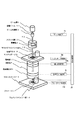
第8図は本発明の転写方法を適用可能な半導体デバイス製造用露光装置の一例の概略構成図である。なお、後述する第2ないし第3の実施形態も同様の装置を用いるものとする。
【0020】
この半導体デバイス製造用露光装置の制御は、ビーム源1から放射されたビーム12のドーズ量を制御するビーム制御部2aと、マスクステージ6を移動させるマスクステージ制御部6aと、偏向器15を制御する偏向器制御部15aと、ウエハ10へ照射される転写マスク3のパターンの倍率を補正する倍率補正系8を制御する倍率補正制御部8aと、ウエハステージ11を移動させるウエハステージ制御部11aとを有する装置制御部16によりなされる。
【0021】
まずビーム源1から放射される電子ビームもしくはイオンビーム等、荷電粒子線である荷電ビーム12は、ビーム制御部2aによるビーム制御系2のon/offを行うことでドーズ量が制御されて照明系4に入射し、これによりマスクステージ6上の転写マスク3に照射される。
【0022】
ここで照明系4内には、円弧形状のスリットが形成されたスリット板13が設けられており、照明系4を通った荷電ビーム12は光軸と垂直な平面内で円弧形状に成形される。このようにビーム形状を円弧形状にすることで、結像位置は光軸から離れた荷電ビーム12の外周付近となる。これにより、像面湾曲を無視できるほどに抑制しつつ、露光領域の拡大を図ることが可能となる。本実施形態では、荷電ビーム12は円弧形状のビーム形状を用いているが、ビーム形状はそれ以外の形状でもかまわない。
【0023】
マスクステージ6はマスクアライメント系5により測定、演算処理された補正値に基づき、マスクステージ制御部6aにより駆動されることで、転写マスク3と転写ビーム12との位置合わせを行う。
【0024】
転写マスク3に照射された荷電ビーム12は、転写マスク3上のパターンを偏向器15により偏向後、投影系7に投影され、さらに倍率補正系8により投影倍率が補正された後、ウエハステージ11上のウエハ10に照射され、これにより転写マスク3のパターンが転写される。
【0025】
なお、ウエハステージ制御部11aにより制御されるウエハステージ11は、ウエハライメント系14により測定、演算処理された値に基づき、ウエハ10の位置合わせを行う。転写の際にはあらかじめ、マスクステージ6とウエハステージ11は互いのステージの走査移動方向や直交度、相対走査方向のパターン倍率等を合わせ、その座標系を基準座標系として以後の全ての工程の基準とする。
【0026】
次に、図5の転写マスク3をいわゆる1stマスクとしてウエハ10に焼きつける工程で本発明の転写方法を説明する。
【0027】
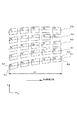
図5は、5×5の配列に分割された部分転写パターンをもつ、転写マスク3と、転写マスク3上の部分転写パターンであるマスクショット3a〜3yをウエハ10上に焼きつけた転写像101をそれぞれ表している。
【0028】
各マスクショット3a〜3yは転写像101を複数に分割したものである。転写マスク3上の各マスクショット3a〜3yの周囲には、各マスクショット3a〜3yの転写マスク3上での位置を規定するためのマークであるアライメントマーク3a1〜3y6が配置されている。
【0029】
たとえばマスクショット3aの位置は、アライメントマーク3a1〜3a6で定義されることとなる。これら転写マスク3上の各マスクショット3a〜3yは、マスクショット3aがウエハ10上のショットであるウエハショット10aに、マスクショット3bがウエハショット10bに、といった具合に順次隙間なくウエハ10上に転写され、所望の転写像101が得られる。この際にマスクショット3a〜3e、3f、3j、3k、3o、3p、3t、3u〜3y、のアライメントマークのうち転写像の外周部にある、例えば3a1、3a2、3a5、3a6等もウエハ10上に転写され、2ndレイヤ以降のアライメントに用いられる。
【0030】
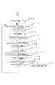
図1は上記の工程の詳細をフローチャートにしたものであり、本発明の基本フローである。
【0031】
以下、図5及び図1のフローを追って順に説明する。なお、ここではウエハ10は既に装置内にロードされているものとしている。
【0032】
まず、転写マスク3をマスクステージ6上にロードし(ステップ20)、次にマスクアライメント系5で転写マスク3の位置を計測し、マスクステージ6を駆動して基準位置合わせを行う(ステップ21)。このときの基準は先述した基準座標系で、この基準座標系に荷電ビーム12の基準軸や別に設けられた装置基準が合致している。したがって、この基準位置合わせは転写マスク3を荷電ビーム12の基準軸や別に設けられた装置基準に対して位置合わせをすることに他ならない。
【0033】
転写マスク3が基準位置に配置されると、アライメントで計測に用いるアライメントマークを指定する(ステップ22)。ここでは、マスクショット3a、3c、3e、3f、3h、3j、3k、3m、3o、3p、3r、3t、3u、3w、3yに対応する各アライメントマーク3a1〜3a4、3c1〜3c4、3e1〜3e4、3f1〜3f4、3h1〜3h4、3j1〜3j4、3k1〜3k4、3m1〜3m4、3o1〜3o4、3p1〜3p4、3r1〜3r4、3t1〜3t4、3u1〜3u4、3w1〜3w4、3y1〜3y4、を指定する。このステップで全てのマスクショットのアライメントマークを指定してもよいが、計測するマークの数が多いはど計測時間が長くなるので、装置のスループットが低下することに留意する必要がある。
【0034】
次に、ステップ22で指定された転写マスク3上の各マスクショット3a、3c、3e、3f、3h、3j、3k、3m、3o、3p、3r、3t、3u、3w、3yに各々対応するアライメントマーク3a1〜3a4、3c1〜3c4、3e1〜3e4、3f1〜3f4、3h1〜3h4、3j1〜3j4、3k1〜3k4、3m1〜3m4、3o1〜3o4、3p1〜3p4、3r1〜3r4、3t1〜3t4、3u1〜3u4、3w1〜3w4、3y1〜3y4の位置をマスクアライメント系5で計測する(ステップ23)。
【0035】
すなわち、マスクショット3aでは、アライメントマーク3a1、3a2、3a3、3a4の位置が計測される。ここでアライメントマーク3a5、3a6を指定してもかまわないが、アライメントマーク3a1〜3a4の位置が分かればマスクショット3aの位置を特定することができるので敢えて指定はしなくてもよい。
【0036】
マスクショット3a、3c、3e、3f、3h、3j、3k、3m、3o、3p、3r、3t、3u、3w、3yの各アライメントマークの位置を計測した後、各アライメントマーク3a1〜3a4、3c1〜3c4、3e1〜3e4、3f1〜3f4、3h1〜3h4、3j1〜3j4、3k1〜3k4、3m1〜3m4、3o1〜3o4、3p1〜3p4、3r1〜3r4、3t1〜3t4、3u1〜3u4、3w1〜3w4、3y1〜3y4の位置をマーク毎に記憶しておく(ステップ24)。
【0037】
次に、ステップ24で記憶した各アライメントマーク3a1〜3a4、3c1〜3c4、3e1〜3e4、3f1〜3f4、3h1〜3h4、3j1〜3j4、3k1〜3k4、3m1〜3m4、3o1〜3o4、3p1〜3p4、3r1〜3r4、3t1〜3t4、3u1〜3u4、3w1〜3w4、3y1〜3y4の位置を読み出してマスクショット3a〜3yの位置を定める関数を算出する(ステップ25)。
【0038】
図6はアライメントマークの位置データから得られた関数を表す図である。関数の算出はストライプ毎に行い、例えばマスクショット3a〜3eで構成されるストライプの関数は3s1の様になる。同様にマスクショット3f〜3jに対して3s2、マスクショット3k〜3oに対して3s2、マスクショット3p〜3tに対して3s4、マスクショット3u〜3yに対して3s5を算出する。
【0039】
関数の求め方としては、N次関数近似、累乗関数近似、多項式関数近似、スプライン補完等、一般に知られている種々の方法を用いることができる。更に、これらの関数と実際のマーク位置との距離を誤差最小自乗法などで評価して、実際のマーク位置に対して最もよくフィットするものを採用してもよい。
【0040】
次に相対走査方向のパターン倍率を求める為にマスクストライプ長を算出する。例えばマスクショット3aのアライメントマーク3a1とマスクショット3eのアライメントマーク3e4との相対走査方向の距離と、マスクショット3aのアライメントマーク3a2とマスクショット3eのアライメントマーク3e3の相対走査方向の距離との平均値をこのマスクストライプのマスクストライプ長ds1として算出する。同様にして各マスクストライプのマスクストライプ長ds2〜ds5を算出する。これらマスクストライプ長ds1〜ds5の平均値dsmを転写マスク3の設計上のマスクストライプ長dsで除した値dsm/dsを第1のパターン倍率である相対走査方向のパターン倍率Smmとする。
【0041】
以上のようにして得られた各ストライプの関数3s1〜3s5と相対走査方向のパターン倍率Smmを記憶しておく(ステップ26)。
【0042】
ここまでのステップで各マスクストライプに対する関数と転写マスク3の相対走査方向のパターン倍率が決定され記憶されたことになる。以降のステップではステップ25で求めた関数をもとに各マスクショットの転写開始位置を決定して実際の露光処理へ移ってゆく。
【0043】
ステップ24で記憶しておいた各マスクショットのアライメントマーク位置とステップ25で算出した関数から各マスクショットの転写開始位置を算出する(ステップ27)。
【0044】
各マスクショットの転写開始位置の算出には種々の方法が考えられるが、例えばマスクショット3aに対しては、アライメントマーク3a1とアライメントマーク3a2の相対走査方向、すなわち、x座標の平均値に、アライメントマークから転写開始位置までの設計上のオフセット値にステップ25で算出した相対走査方向のパターン倍率Smmを乗じたもの、を加えた値を転写開始位置のx座標とし、同様に転写終了位置のx座標も算出することができる。
【0045】
ここでステップ22で全てのマスクショットを指定している場合には、前述の処理を全てのマスクショットに対して行い各マスクショットの転写開始位置を求めればよい。ステップ22で全てのマスクショットを指定していない場合、例えば本実施形態のような場合にマスクショット3bの転写開始位置と転写終了位置を求めるには、まず先述の手順でマスクショット3aの転写開始位置と転写終了位置を求め、同様にしてマスクショット3cの転写位置と転写終了位置を求めた後、マスクショット3aの転写開始位置のx座標とマスクショット3cの転写開始位置のx座標との中点を算出すればよい。また転写終了位置についても同様に算出すればよい。ここで中点を用いたのはマスクショット3bの設計上の位置がマスクショット3aとマスクショット3cの中央に配置されているためであり、ステップ22での計測マスクショットの指定の仕方と各マスクショットの設計上の配置から決定されることはいうまでもない。
【0046】
このようにして算出した各マスクショットの転写開始位置と転写終了位置を記憶しておく(ステップ28)。
【0047】
次に、ステップ26で記憶しておいた相対走査方向のパターン倍率Smmを読み出して、マスクステージ6のx方向の駆動速度の倍率である駆動倍率として設定する(ステップ29)。
【0048】
露光処理が開始されると(ステップ30)、マスクショット番号nが1に初期化され(ステップ31)、以降のショット露光のループに進む。
【0049】
n=1のとき、マスクショット3aとなる。このループの最初は、まずステップ28で記憶した1番目のマスクショット3aの転写開始位置を読み出す(ステップ32)。
【0050】
次に、x、y、θ軸を有するマスクステージ6を駆動して、読み出した転写位置にマスクショット3aを移動させる(ステップ33)。この動作と同時にウエハステージ11を駆動し(ステップ34)、ウエハ10を1番目のマスクショット3aが転写されるべき位置に移動する。これらステップ33及びステップ34で駆動された各ステージの位置は相対走査の開始位置である。
【0051】
次に、ステップ26で記憶しておいた関数のうち当該マスクショット、この場合マスクショット3aが含まれるマスクストライプの関数3s1を読み出す(ステップ35)。この段階でこのショットに対する、露光準備ができたことになる。
【0052】
次に、ビーム制御系2を駆動して荷電ビーム12をマスクショット3aに照射してウエハ10上のウエハショット10aとして転写を開始し、マスクステージ6とウエハステージ11とを荷電ビーム12に対して相対走査しながらマスクショット3aの全域をウエハ10上に転写する(ステップ36)。このときマスクステージ6はステップ35で読み出した関数3s1上をトレースするように駆動する。この関数上をトレースするということが本発明の最大の特徴であり、このことによって各マスクショットがもっている湾曲や歪みの補正を可能にしているのである。
【0053】
このショットに対する露光が完了すると、全てのショットの露光が完了したかどうかを判別する(ステップ37)。まだ全てのショットの露光が完了せず、次のショットの露光を行うなら、マスクショット番号nに1を加え(ステップ38)、ステップ32に戻る。
【0054】
このステップ32〜ステップ38のループを繰り返し、マスクショット3b〜3yについても同様の処理を行う。全てのマスクショット3a〜3yに対する処理が完了すると、このループから抜け出し、次のチップ処理工程へ進む(ステップ39)。これでウエハ10上に所望のチップないしパターン1個が転写されたことになる。なお、ウエハ10上に複数のチップを転写するためには、上記フローのステップ31〜ステップ39までをチップの数だけ繰り返せばよい。
【0055】
以上の通り、転写マスク3上の部分転写パターンに対応するアライメントマークのうちの幾つかを指定して、それらの位置から各マスクストライプ毎の関数を求め、転写に際してはそれらの関数上をトレースしながら各マスクショットを相対走査することで、各部分転写パターンの湾曲や歪みを補正することができ、アライメントに要する時間を短縮しつつ繋ぎ精度の高い転写像101を得ることができる。
(第2の実施形態)
本実施形態では、マスクショットの相対走査方向に直交する方向、すなわち、y軸方向のパターン倍率にも着目し補正を可能にすることで、部分転写パターンの繋ぎ精度をさらに改善している。この方法は、マスクショットの相対走査方向のパターン倍率とそれに直交する方向のパターン倍率に差がある場合に有効である。以降、第1の実施形態の説明で用いた図5のマスクショットレイアウト、図2及び図3に示すフローチャートを用いて、本実施形態の転写方法を説明する。
【0056】
まず、図2のフローチャートのステップ20〜ステップ26は先述の第1の実施形態と同様で、図5の転写マスクを装置にロードして基準合わせを行った後、指定されたアライメントマークの計測を行う。指定するアライメントマークは第1の実施形態と同じであるが、全てのマークを指定してもよく、本実施形態では後述するように、全てのマークを指定すると最大の効果が得られる。アライメントマークの計測から各マークの位置を求めて、各マスクストライプに対応する関数と転写マスク3の相対走査方向のパターン倍率Smmを算出し記憶しておく(ステップ26)。
【0057】
次に、ステップ24で記憶した各アライメントマークの位置を読み出して各マスクショットの相対走査方向と直交する方向のパターン倍率Mvnを算出する(ステップ200)。
【0058】
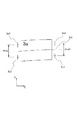
ここでの処理は、図7に示すように例えばマスクショット3aに関して、アライメントマーク3a1と3a2の実際のマーク位置の間隔をdva1とし、同様にアライメントマーク3a3と3a4の実際のマーク位置間隔をdva3とするとき、それらの平均値を設計上のマーク間隔Dvfで除した値、(dva1+dva3)/2Dvfを相対走査方向と直交する方向のパターン倍率Mv1として算出する。ここでステップ22で全てのマスクショットを指定していない場合は、指定した各マスクショットの相対走査方向と直交する方向のパターン倍率Mvnの平均値を求め、第3のパターン倍率である各マスクショットの相対走査方向と直交する方向の平均パターン倍率をMmとして記憶しておく(ステップ201)。また、ステップ22で全てのマスクショットが指定されている場合は、第2のパターン倍率である全てのマスクショットの相対走査方向と直交する方向のパターン倍率Mvnを各マスクショット毎にステップ201で記憶しておく。
【0059】
次に、ステップ22の計測マーク指定が全てのマスクショットに対して為されているかどうかを判別し(ステップ202)、全てに対して為されていれば、ステップ203〜ステップ205をスキップし、そうでなければステップ203を実行するように分岐させる。この理由は各マスクショットの相対走査方向と直交する方向の平均パターン倍率Mmを用いる場合には、あらかじめ倍率補正系8を駆動して(ステップ204)、全てのマスクショットに対して同じ量の補正を行うことが可能だからである。
【0060】
これに対してステップ22で全てのマスクショットが指定されていれば、各々のマスクショットに対して、各々に最適な個別の相対走査方向と直交する方向のパターン倍率Mvbでの補正が可能となる。この場合は後述するショット露光のループのなかで各ショット毎に倍率補正系8を駆動して補正を行う必要がある。このため、全てのマスクショットが指定されている場合は、ステップ203〜ステップ205をスキップする。
【0061】
ここでステップ22で全てのマスクショットが指定されていれば、ステップ201で記憶しておいた各マスクショットの相対走査方向と直交する方向の平均パターン倍率Mmを読み出し(ステップ203)、倍率補正系8を駆動してマスクショットに対する倍率補正を行う(ステップ204)。
【0062】
次に、ステップ26で記憶しておいた相対走査方向のパターン倍率Smmと各マスクショットの相対走査方向と直交する方向の平均パターン倍率Mmからマスクステージ6の駆動速度の倍率である駆動倍率を求め設定する(ステップ205)。この理由は本実施形態における倍率補正系8の補正形態が、荷電ビーム12の光軸に軸対称に作用するように構成されているためで、この場合の相対走査方向のパターン倍率はSmmを倍率補正系8に与えた補正値Mmで除した値Smm/Mmとなる。ここで倍率補正系8の補正形態が相対走査方向と直交する方向のみに作用するような構成であれば、相対走査方向のパターン倍率Smmをそのまま用いればよい。
【0063】
以降、第1の実施形態と同様に、各マスクショットの転写開始位置と転写終了位置を算出し(ステップ206)、記憶した後(ステップ207)、一連の露光処理が開始する(ステップ208)。
【0064】
次に、図3において、第1の実施形態と同様にマスクショット番号nが1に初期化されて(ステップ209)、ショット露光のループであるステップ210〜ステップ220へ進む。
【0065】
次に、計測マーク指定が全てのマスクショットに対して為されているかどうかを判別する(ステップ210)。
【0066】
ステップ22で全てのマスクショットを指定している場合、すなわち、パターン倍率の補正を各マスクショット毎に行うのであれば、ステップ201で記憶しておいた当該マスクショットの相対走査方向と直交する方向のパターン倍率Mvnを読み出して(ステップ211)、倍率補正系8を駆動して相対走査方向と直交する方向のパターン倍率を補正し(ステップ212)、同時に当該ショットの相対走査方向のパターン倍率として、Smm/Mvnをマスクステージ6の駆動倍率として設定する。
【0067】
ステップ22で全てのマスクショットを指定していない場合、すなわち、各マスクショットの相対走査方向と直交する方向の平均パターン倍率Mmを用いて、全てのマスクショットに対して同じ量の補正を与えるならば、すでにステップ204で倍率補正系8を各マスクショットの相対走査方向と直交する方向の平均パターン倍率Mmに基づいて駆動してあるので、ステップ211〜ステップ213をスキップする。
【0068】
ステップ214〜ステップ217は第1の実施形態と同様で、当該マスクショットの転写開始位置を読み出して(ステップ214)、マスクステージ6を駆動し(ステップ215)、そのマスクショットの転写像がウエハ10上の転写されるべき位置にくるようにウエハステージ11を駆動し(ステップ216)、当該マスクショットに対応するマスクストライプの関数を読み出し(ステップ217)、相対走査露光の開始に備える。
【0069】
以降、そのショットに対してマスクステージ6を関数上をトレースするように駆動しながら相対走査露光を行い(ステップ218)、ショットひとつ分の処理が終了する。
【0070】
これ以降の各ステップは第1の実施形態と同様で、ショットの数だけステップ210〜ステップ220のループを繰り返し、全てのショットの露光が完了したかどうかを判別し(ステップ219)、全てのショットの露光が完了しておらず、次のショットの露光を行うなら、マスクショット番号nに1を加え(ステップ220)、ステップ210へ戻り、全てのショットの露光が完了したなら、次のチップ処理工程へ進む(ステップ221)。
【0071】
以上の通り、本実施形態では各ショットの相対走査方向と直交する方向のパターン倍率にも着目し補正することで、更に繋ぎ精度の高い転写像101を得ることができる。
【0072】
以上の通り、第1の実施形態に加えて、部分転写パターンの相対走査方向に直交する方向のパターン倍率を補正することでさらに繋ぎ精度の高い転写像101を得ることができる。
(第3の実施形態)
第1ないし第2の実施形態では、部分転写パターンの露光に際して、各部分転写パターンの転写開始位置にウエハを移動してその後相対走査によって露光する、いわゆるステップ・アンド・スキャン方式に本発明を適用した例について説明した。これに対して本実施形態では、各部分転写パターンを転写する際に、各マスクストライプ毎に、ひとつのマスクショットから次のマスクショットヘマスクステージ6とウエハステージ11を停止させることなく連続移動させながら、転写するように構成してある。こうすることで応答速度の遅い機械式ステージの急激な加減速や停止による時間のロスを抑えて、装置全体のスループットを更に向上させている。また本実施形態では、相対走査方向と直交する方向のパターン倍率と相対走査方向のパターン倍率を各マスクストライプ毎に補正する方式を採用しており、繋ぎ合わせ精度の向上をも図っている。
【0073】
以降、図5のマスクショットレイアウト及び図4に示すフローチャートを用いて、本実施形態の転写方法を説明する。
【0074】
まず、図4のフローチャートのステップ20〜ステップ26は先述の第1の実施形態と同様で、図5の転写マスク3を装置にロードして基準合わせを行った後、指定されたアライメントマークの計測を行う。指定するアライメントマークは第1の実施形態と同じであるが、全てのマークを指定してもよい。アライメントマークの計測から各マークの位置を求めて、各マスクストライプに対応する関数3s1〜3s5を求める。また本実施形態では第4のパターン倍率である各マスクストライプ毎の相対走査方向のパターン倍率Sm1〜Sm5を算出し関数3s1〜3s5とともに記憶しておく(ステップ26)。なお、ここでの相対走査方向のパターン倍率は、先述の第1の実施形態と同じ方法で求めた、各マスクストライプの相対走査方向のパターン倍率を平均することなく、そのまま用いればよい。
【0075】
次に、ステップ24で記憶した各アライメントマークの位置を読み出して各マスクストライプ毎の平均パターン倍率Mm1〜Mm5を算出し(ステップ300)、各マスクストライプ毎に記憶しておく(ステップ301)。各マスクショットのパターン倍率を算出する方法は第2の実施形態と同じであり、それらをマスクストライプ毎に平均してMm1〜Mm5を得ている。
【0076】
次に、各マスクストライプの転写開始位置を算出する(ステップ302)が、例えばマスクショット3a〜マスクショット3eに対応するマスクストライプの転写開始位置として第1の実施形態におけるマスクショット3aの転写開始位置を、転写終了位置としてマスクショット3eの転写終了位置を、各々採用すればよい。このようにして、全てのマスクストライプの転写開始位置と転写終了位置を算出して記憶する(ステップ303)。
【0077】
以降、一連の露光処理が開始されると(ステップ304)、マスクストライプ番号Nが1に初期化されて(ステップ305)、ストライプ露光のループであるステップ306〜ステップ315へ進む。
【0078】
次に、ステップ301で記憶しておいたマスクストライプNに対応する平均パターン倍率MmNを読み出して(ステップ306)、倍率補正系8を駆動して相対走査の方向に直交する方向のパターン倍率を補正する(ステップ307)。
【0079】
さらに、ステップ26で記憶しておいた当該マスクストライプNの相対走査方向のパターン倍率SmNを読み出し、先述の第2の実施形態と同じ理由からSmN/MmNをもってマスクステージ6の駆動速度の倍率である駆動倍率として設定する(ステップ308)。
【0080】
次にステップ303で記憶しておいた、当該マスクストライプNの転写開始位置を読み出し(ステップ309)、マスクステージ6を移動させる(ステップ310)と同時に、ウエハステージ11を駆動して(ステップ311)、ウエハ10を当該マスクストライプNが転写されるべき位置に移動させる。さらにステップ26で記憶しておいた当該マスクストライプNの関数3sNを読み出し(ステップ312)、当該マスクストライプNに対する走査露光の準備が完了する。
【0081】
以降、マスクストライプNに対して荷電ビーム12が関数3sN上をトレースするように相対走査露光を行う(ステップ313)。本実施形態では相対走査工程をマスクステージ6と、ウエハステージ11と、偏向器15とを用いて行っている。すなわち、マスクステージ6とウエハステージ11を各々の転写開始位置から直線状に相対駆動させておいて、関数3s1のトレースは偏向器15を駆動することで実現している。この理由は、転写マスク3及びウエハ10の連続移動中に各マスクショット間に存在する梁状の領域を関数3s1に沿ってスキップさせる必要があるからである。
【0082】
本発明の主眼はマスクストライプ毎の関数上をトレースさせて各マスクストライプの部分転写パターンの湾曲や歪みを補正することにあるので詳述しないが、各マスクショット間に存在する梁状の領域をスキップさせるには以下のように転写を行う。
【0083】
例えば、マスクショット3aの相対走査による転写が終了し、荷電ビーム12が次に転写するべきマスクショット3bの転写開始位置に到達した時点でマスクショット3bの転写像を偏向器15を用いて関数3s1に沿ってウエハ10に対して移動させて、ウエハ10上に既に転写されているマスクショット3aの転写パターンに繋ぎ合わせるようにすればよい。
【0084】
また、偏向器15の数や配置によって様々な方法が考えられるが、どのような手法を用いても各マスクショットを関数上をトレースしながら相対走査して露光することの効果に変わりはない。以上のようにしてストライプひとつ分の処理が終了する。
【0085】
これ以降の各ステップは、ステップ306〜ステップ315のループを繰り返し、全てのストライプの露光が完了したかどうかを判別し(ステップ314)、まだ全てのストライプの露光が完了せず、次のストライプの露光を行うなら、ストライプ番号Nに1を加え(ステップ315)、ステップ306に戻る。全てのストライプに対する処理が完了すると、このループから抜け出し、次のチップ処理工程へ進む(ステップ316)。
【0086】
以上、述べたように、各マスクストライプ毎に、ひとつのマスクショットから次のマスクショットヘマスクステージ6とウエハステージ11を停止させることなく連続移動させながら、転写するように構成することで、各ステージの急激な加減速や停止による時間のロスを抑えて、装置全体のスループットを更に向上させると同時に、相対走査方向と直交する方向のパターン倍率と相対走査方向のパターン倍率を各マスクストライプ毎に補正して、繋ぎ合わせ精度の向上を図ることができる。
【0087】
以上説明した、第1ないし第3の実施形態からわかるように、マスクショットの補正曲線による補正は、マスクステージで実行している。しかしながら、マスクとウエハは転写系によって決まる一定の相対関係があるため、マスクステージのかわりにウエハステージによっても同様な補正が可能である。この様な配慮は、各々のステージの機能や性能、駆動精度等によって選択することで、ショットの繋ぎ合わせ精度を一段と向上させることができる。また、本発明はあらゆる転写方式、たとえば等倍投影転写系、縮小投影転写系、近接転写系、密着転写系等の方式に適用ができる。また、第1ないし第3の実施形態はいわゆる1stレイヤに本発明を適用しているが、いわゆる2ndレイヤ以降のレイヤであってもその効果は何ら変わるものではない。その場合、ウエハ上のチップのアライメント方法は従来の光露光装置などで採用されている種々の方法を用いることができ、例えばグローバルアライメント方式では、ウエハ上のチップの並び方を計測して、その並び方を理論上の並び方と比較してチップの並び方に関する座標系を補正する。この補正された座標系を用いてウエハステージを駆動するようにしておいて、その上で更に本実施形態を適用すればよいのである。
【0088】
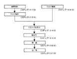
次に上記説明したマスクパターン転写方法を利用したデバイス製造方法の実施形態を説明する。図9は微小デバイス(ICや1SI等の半導体チップ、液晶パネル、CCD、薄膜磁気ヘッド、マイクロマシン等)の製造フローを示す。ステップ1010(回路設計)ではデバイスのパターン設計を行う。ステップ1020(マスク製作)では設計したパターンを形成したマスクを製作する。一方、ステップ1030(ウエハ製造)ではシリコンやガラス等の材料を用いてウエハを製造する。ステップ1040(ウエハプロセス)は前工程と呼ばれ、上記用意したマスクとウエハを用いて、リソグラフィ技術によってウエハ上に実際の回路を形成する。次のステップ1050(組み立て)は後工程と呼ばれ、ステップ1040によって作製されたウエハを用いて半導体チップ化する工程であり、アッセンブリ工程(ダイシング、ボンディング)、パッケージング工程(チップ封入)等の工程を含む。ステップ1060(検査)ではステップ1050で作製された半導体デバイスの動作確認テスト、耐久性テスト等の検査を行う。こうした工程を経て半導体デバイスが完成し、これが出荷(ステップ1070)される。図10は上記ウエハプロセスの詳細なフローを示す。ステップ1110(酸化)ではウエハの表面を酸化させる。ステップ1120(CVD)ではウエハ表面に絶縁膜を形成する。ステップ1130(電極形成)ではウエハ上に電極を蒸着によって形成する。ステップ1140(イオン打込み)ではウエハにイオンを打ち込む。ステップ1150(レジスト処理)ではウエハにレジストを塗布する。ステップ1160(露光)では上記説明した露光装置または露光方法によってマスクの回路パターンをウエハの複数ショット領域にならべて焼付露光する。ステップ1170(現像)では露光したウエハを現像する。ステップ1180(エッチング)では現像したレジスト像以外の部分を削り取る。ステップ1190(レジスト剥離)ではエッチングが済んで不要になったレジストを取り除く。これらのステップを繰り返し行うことによって、ウエハ上に多重に回路パターンが形成される。本実施形態の生産方法を用いれば、従来は製造が難しかった大型のデバイスを低コストに製造することができる。
【0089】
【発明の効果】
以上説明したように、あらかじめ、所望の部分転写マスクのアライメントマークを指定し、指定された部分転写パターンの各アライメントマークの位置を計測し、これを基に各部分転写パターンの位置を定める関数を定めておき、さらに各アライメントマークの位置を基に転写の倍率を求めておき、これら関数及び転写の倍率を用いて被転写物に部分転写パターンを転写することで、高いスループットを維持しつつ、高精度な繋ぎ合わせが可能となった。さらに、走査露光工程で、転写マスクと被転写物とを連続して相対走査させることによりさらに、スループットの向上を図ることができた。
【図面の簡単な説明】
【図1】本発明の第1の実施形態でのマスクショットの転写方法を説明するフローチャートである。
【図2】本発明の第2の実施形態でのマスクショットの転写方法を説明するフローチャートである。
【図3】本発明の第2の実施形態でのマスクショットの転写方法を説明するフローチャートである。
【図4】本発明の第3の実施形態でのマスクショットの転写方法を説明するフローチャートである。
【図5】第1ないし第3の実施形態でのマスクショット及びウエハショットを説明する概略図である。
【図6】本発明におけるマスクショットの位置を定める関数を説明する概略図である。
【図7】本発明におけるマスクショット3aのパターン倍率を説明する概略図である。
【図8】本発明の転写方法を適用可能な半導体デバイス製造用露光装置の一例の概略構成図である。
【図9】デバイス製造工程を示すフローチャートである。
【図10】図9に示したウエハプロセスの詳細な工程を示すフローチャートである。
【符号の説明】
1 ビーム源
2 ビーム制御系
2a ビーム制御部
3 転写マスク
3a1〜3y6 アライメントマーク
3a〜3e マスクショット
3s1〜3s5 部分転写パターンの位置を定める関数
4 照明系
5 マスクアライメント系
6 マスクステージ
6a マスクステージ制御部
7 投影系
8 倍率補正系
8a 倍率補正制御部
10 ウエハ
11 ウエハステージ
11a ウエハステージ制御部
12 荷電ビーム
13 スリット
14 ウエハライメント系
15 偏向器
16 装置制御部
101 転写像[0001]
BACKGROUND OF THE INVENTION
The present invention relates to a transfer method for manufacturing a device by transferring a fine pattern on a mask onto a substrate such as a wafer or glass.
[0002]
[Prior art]
As the degree of integration of semiconductor devices has increased and performance and functions have improved, the resolution and resolution of lithographic equipment has increased, and the transfer method has been changed to a step-and-repeat method through a wafer batch method, step-and-repeat method, It is changing to the AND scan method. Under such circumstances, a scanning reduction transfer system using a transfer mask has been proposed for an exposure apparatus using a charged beam such as an electron beam, which can be expected to have higher resolution.
[0003]
However, with this type of device, if the angle of view is widened, the image performance is remarkably reduced, and due to restrictions on the structure of the mask used, the transfer pattern is divided into multiple patterns. The desired patterns are obtained by sequentially connecting and transferring the transferred patterns.
[0004]
The division mask is obtained by arranging transfer patterns divided on a single mask substrate at predetermined positions.
[0005]
In this transfer method using a divided mask, the accuracy of connection with adjacent transfer patterns is important. Therefore, the divided transfer patterns need to be arranged at a predetermined position on the mask with very high accuracy. However, for example, when this division mask is created using an electron beam drawing apparatus, depending on the drawing method, the transfer pattern and the arrangement of these division masks are curved, or the size of each pattern is as designed. There is not. Further, distortion due to temperature change of the divided mask, distortion due to mechanical stress, distortion due to change with time, and the like also cause errors. These errors deteriorate the above-described splicing accuracy, and as a result, the chip is defective.
[0006]
In order to solve such a problem, for example, as disclosed in Japanese Patent Application Laid-Open No. 63-73520, the position of the entire mask is obtained using a dedicated mark, and temporary data based on the data is obtained. A method is known in which a division pattern to be exposed next is driven to an exposure position using a coordinate system, and then alignment is sequentially performed for each division transfer pattern using an alignment mark dedicated to each division pattern. This method is called a die-by-die method, and an accurate alignment is possible because alignment is performed for each divided pattern.
[0007]
[Problems to be solved by the invention]
However, in the method as described above, each divided pattern is temporarily driven using a temporary coordinate system, and then alignment is performed for each divided transfer pattern using an alignment mark dedicated to the divided pattern. Each pattern transfer requires measurement and driving for alignment, and there is a problem that the measurement time and driving time reduce the throughput of the entire apparatus. This problem has a greater effect on throughput as the number of mask divisions increases.
[0008]
Further, the method disclosed in Japanese Patent Laid-Open No. 63-73520 cannot correct the curvature of the divided pattern itself caused by the drawing method of the electron beam drawing apparatus used in the process of creating the divided mask described above.
[0009]
Furthermore, in contrast to the conventional transfer method in which one chip can be transferred in at least one shot, in the transfer method using such a divided mask, the time taken to transfer one chip is the number of mask divisions. It will increase with. For example, one chip is divided into a 5 × 10 matrix array and arranged on a mask, and each divided pattern is transferred and connected sequentially, and all 50 divided patterns are transferred, and finally one chip. Is completed. If step and scan are simply repeated, the load is 50 times the number of scans and 5 times the exposure time.
[0010]
Therefore, in order to save the time required for extreme acceleration / deceleration or stop of the stage on which the wafer or mask is placed, the transfer is performed at a higher speed by continuously moving from one divided pattern to another without stopping the stage. A system that enables this is conceivable.
[0011]
However, the above-described die-by-die alignment method cannot be used if the transfer is performed while continuously moving the mask or wafer. This is because, as described above, it is necessary to position each divided pattern once using a temporary coordinate system, and then perform alignment for each divided transfer pattern using an alignment mark dedicated to the divided pattern. is there.
[0012]
Accordingly, the present invention provides a mask pattern transfer method for improving the splicing accuracy of each partial transfer pattern while improving the throughput when a desired pattern is obtained by sequentially transferring a plurality of divided partial transfer patterns to a transfer object. Another object of the present invention is to provide an apparatus, a device manufacturing method, and a transfer mask.
[0013]
[Means for Solving the Problems]
In order to achieve the above object, a mask pattern transfer method according to the present invention provides a transfer mask having a plurality of distinguishable partial transfer patterns divided and arranged in a predetermined direction and a direction intersecting the predetermined direction. The transfer object is irradiated with a transfer beam through the transfer mask, and the partial transfer patterns are sequentially transferred to the transfer object, thereby the desired transfer of the partial transfer patterns to the transfer object. In order to form the pattern, a plurality of alignment marks associated with each of the partial transfer patterns is provided on the transfer mask, and the relative position between the transferred object and the alignment marks is corrected, A mask pattern transfer method for sequentially transferring the partial transfer patterns to the transfer object,
The correction of the relative position includes a transfer mask mark designation step for designating each alignment mark,
Measuring the position of each alignment mark specified in the transfer mask mark specifying step, and determining a function for determining the position of each partial transfer pattern arranged in the predetermined direction based on the measured position When,
A scanning exposure step in which the transfer mask and the transfer object are relatively scanned in the predetermined direction with respect to the transfer beam, and the partial transfer pattern is scanned and exposed on the transfer object;
A relative movement step of relatively moving an image of the partial transfer pattern with respect to the transfer object based on the function when the partial transfer pattern is scanned and exposed on the transfer object.
[0014]
In the mask pattern transfer method of the present invention as described above, the alignment mark of the desired partial transfer mask is designated in advance, the position of each alignment mark of the designated partial transfer pattern is measured, and each partial transfer is based on this. Define a function that determines the position of the pattern. The transfer position is corrected based on this function, and the image of the partial transfer pattern is moved relative to the transfer object during scanning exposure. For this reason, it is not necessary to measure the alignment mark and determine the transfer position each time each divided pattern is transferred to the transfer object.
[0015]
The mask pattern transfer apparatus of the present invention comprises a beam radiating means for radiating a charged beam for exposure,
Shaping means for shaping the charged beam into an arc shape;
A plurality of distinguishable partial transfer patterns divided and arranged in a predetermined direction and a direction crossing the predetermined direction for transferring to the transfer object, and each of the partial transfer patterns are associated with each other. A movable first placement means on which a transfer mask on which a plurality of alignment marks are formed is placed;
A movable second mounting means on which a transfer object to which a transfer pattern consisting of each partial transfer pattern of the transfer mask is transferred is mounted;
Magnification correction means for correcting the projection magnification of the charged beam that has passed through the transfer mask and irradiating the transferred object;
First measuring means for measuring the positions of the partial transfer patterns and the alignment marks of the transfer mask;
A second measuring means for measuring a position of the transferred pattern and the alignment marks formed by joining the partial transfer patterns transferred to the transferred object;
Image relative movement means for relatively moving the image of each partial transfer pattern of the transfer mask;
Based on the output signals from the first measuring means and the second measuring means, the driving magnification that defines the moving speed of the first mounting means and the moving speed of the second mounting means are specified. A drive magnification, a projection magnification of the magnification correction unit, and an image relative movement amount of the relative movement unit are calculated, and the first placement unit, the second placement unit, the magnification correction unit, and the relative amount are calculated. Control means for controlling the moving means.
[0016]
The device manufacturing method of the present invention is characterized in that a device is manufactured by a process including the mask pattern transfer method of the present invention.
[0017]
The device manufacturing method of the present invention is characterized by manufacturing a device by using the mask pattern transfer apparatus of the present invention.
[0019]
DETAILED DESCRIPTION OF THE INVENTION
Next, embodiments of the present invention will be described with reference to the drawings.
(First embodiment)
FIG. 8 is a schematic block diagram of an example of an exposure apparatus for manufacturing a semiconductor device to which the transfer method of the present invention can be applied. It should be noted that similar devices are used in second to third embodiments described later.
[0020]
The semiconductor device manufacturing exposure apparatus controls the
[0021]
First, the charged amount of a charged
[0022]
Here, the
[0023]
The
[0024]
The charged
[0025]
The wafer stage 11 controlled by the wafer stage control unit 11a aligns the wafer 10 based on values measured and calculated by the wafer alignment system 14. Prior to the transfer, the
[0026]
Next, the transfer method of the present invention will be described in the step of baking the wafer 10 as a so-called 1st mask using the
[0027]
FIG. 5 shows a
[0028]
Each of the
[0029]
For example, the position of the mask shot 3a is defined by the alignment marks 3a1 to 3a6. The
[0030]
FIG. 1 is a flow chart showing the details of the above steps, and is a basic flow of the present invention.
[0031]
Hereinafter, the flow will be described in order with reference to the flow of FIGS. Here, it is assumed that the wafer 10 is already loaded in the apparatus.
[0032]
First, the
[0033]
When the
[0034]
Next, it corresponds to each mask shot 3a, 3c, 3e, 3f, 3h, 3j, 3k, 3m, 3o, 3p, 3r, 3t, 3u, 3w, 3y on the
[0035]
That is, in the mask shot 3a, the positions of the alignment marks 3a1, 3a2, 3a3, 3a4 are measured. Here, the alignment marks 3a5 and 3a6 may be specified. However, if the positions of the alignment marks 3a1 to 3a4 are known, the position of the mask shot 3a can be specified.
[0036]
After measuring the position of each alignment mark of the
[0037]
Next, the alignment marks 3a1-3a4, 3c1-3c4, 3e1-3e4, 3f1-3f4, 3h1-3h4, 3j1-3j4, 3k1-3k4, 3m1-3m4, 3o1-3o4, 3p1-3p4 stored in
[0038]
FIG. 6 is a diagram illustrating a function obtained from the position data of the alignment mark. The calculation of the function is performed for each stripe. For example, the function of the stripe constituted by the
[0039]
As a method for obtaining the function, various generally known methods such as N-order function approximation, power function approximation, polynomial function approximation, and spline interpolation can be used. Further, the distance between these functions and the actual mark position may be evaluated by an error least square method or the like, and the one that best fits the actual mark position may be employed.
[0040]
Next, the mask stripe length is calculated in order to obtain the pattern magnification in the relative scanning direction. For example, the average value of the distance in the relative scanning direction between the alignment mark 3a1 of the mask shot 3a and the alignment mark 3e4 of the mask shot 3e and the distance in the relative scanning direction of the alignment mark 3a2 of the mask shot 3a and the alignment mark 3e3 of the
[0041]
The stripe functions 3s1 to 3s5 and the pattern magnification Smm in the relative scanning direction obtained as described above are stored (step 26).
[0042]
The function for each mask stripe and the pattern magnification in the relative scanning direction of the
[0043]
The transfer start position of each mask shot is calculated from the alignment mark position of each mask shot stored in
[0044]
Various methods are conceivable for calculating the transfer start position of each mask shot. For example, for the mask shot 3a, alignment is performed in the relative scanning direction of the alignment mark 3a1 and the alignment mark 3a2, that is, the average value of the x coordinates. A value obtained by multiplying the design offset value from the mark to the transfer start position by the pattern magnification Smm in the relative scanning direction calculated in
[0045]
Here, if all mask shots are designated in
[0046]
The transfer start position and transfer end position of each mask shot calculated in this way are stored (step 28).
[0047]
Next, the pattern magnification Smm in the relative scanning direction stored in
[0048]
When the exposure process is started (step 30), the mask shot number n is initialized to 1 (step 31), and the process proceeds to the subsequent shot exposure loop.
[0049]
When n = 1, the mask shot 3a is obtained. At the beginning of this loop, first, the transfer start position of the first mask shot 3a stored in step 28 is read (step 32).
[0050]
Next, the
[0051]
Next, the mask stripe function 3s1 including the mask shot, in this case the mask shot 3a, is read from the functions stored in step 26 (step 35). At this stage, this shot is ready for exposure.
[0052]
Next, the
[0053]
When the exposure for this shot is completed, it is determined whether or not all shots have been exposed (step 37). If the exposure of all shots has not been completed yet and the next shot is to be exposed, 1 is added to the mask shot number n (step 38), and the process returns to step 32.
[0054]
The loop of step 32 to step 38 is repeated, and the same processing is performed for the
[0055]
As described above, some of the alignment marks corresponding to the partial transfer pattern on the
(Second Embodiment)
In this embodiment, by focusing attention on the pattern magnification in the direction orthogonal to the relative scanning direction of the mask shot, that is, in the y-axis direction, the correction accuracy of the partial transfer pattern is further improved. This method is effective when there is a difference between the pattern magnification in the relative scanning direction of the mask shot and the pattern magnification in the direction orthogonal thereto. Hereinafter, the transfer method of this embodiment will be described using the mask shot layout of FIG. 5 and the flowcharts shown in FIGS. 2 and 3 used in the description of the first embodiment.
[0056]
First,
[0057]
Next, the position of each alignment mark stored in
[0058]
As shown in FIG. 7, for example, with respect to the mask shot 3a, the processing here is performed by setting the actual mark position interval between the alignment marks 3a1 and 3a2 to dva1, and similarly the actual mark position interval between the alignment marks 3a3 and 3a4 as dva3. Then, a value obtained by dividing the average value by the designed mark interval Dvf, (dva1 + dva3) / 2Dvf, is calculated as the pattern magnification Mv1 in the direction orthogonal to the relative scanning direction. If not all the mask shots are designated in
[0059]
Next, it is determined whether or not the measurement mark designation in
[0060]
On the other hand, if all the mask shots are designated in
[0061]
If all the mask shots are designated in
[0062]
Next, a driving magnification which is a magnification of the driving speed of the
[0063]
Thereafter, as in the first embodiment, the transfer start position and transfer end position of each mask shot are calculated (step 206), stored (step 207), and then a series of exposure processing starts (step 208).
[0064]
Next, in FIG. 3, the mask shot number n is initialized to 1 as in the first embodiment (step 209), and the process proceeds to
[0065]
Next, it is determined whether or not measurement mark designation has been made for all mask shots (step 210).
[0066]
If all mask shots are specified in
[0067]
If not all mask shots are specified in
[0068]
Steps 214 to 217 are the same as in the first embodiment. The transfer start position of the mask shot is read (step 214), the
[0069]
Thereafter, relative scanning exposure is performed on the shot while driving the
[0070]
The subsequent steps are the same as in the first embodiment, and the loop of
[0071]
As described above, in the present embodiment, the
[0072]
As described above, in addition to the first embodiment, by correcting the pattern magnification in the direction orthogonal to the relative scanning direction of the partial transfer pattern, it is possible to obtain a
(Third embodiment)
In the first and second embodiments, the present invention is applied to a so-called step-and-scan method in which exposure of a partial transfer pattern is performed by moving the wafer to a transfer start position of each partial transfer pattern and then performing exposure by relative scanning. An example was described. On the other hand, in this embodiment, when transferring each partial transfer pattern, the
[0073]
Hereinafter, the transfer method of this embodiment will be described using the mask shot layout of FIG. 5 and the flowchart shown in FIG.
[0074]
First,
[0075]
Next, the position of each alignment mark stored in
[0076]
Next, the transfer start position of each mask stripe is calculated (step 302). For example, the transfer start position of the mask shot 3a in the first embodiment is used as the transfer start position of the mask stripe corresponding to the mask shot 3a to the
[0077]
Thereafter, when a series of exposure processing is started (step 304), the mask stripe number N is initialized to 1 (step 305), and the process proceeds to step 306 to step 315 which is a stripe exposure loop.
[0078]
Next, the average pattern magnification MmN corresponding to the mask stripe N stored in
[0079]
Further, the pattern magnification SmN in the relative scanning direction of the mask stripe N stored in
[0080]
Next, the transfer start position of the mask stripe N stored in step 303 is read (step 309), the
[0081]
Thereafter, relative scanning exposure is performed so that the charged
[0082]
The main point of the present invention is to correct the curvature and distortion of the partial transfer pattern of each mask stripe by tracing on the function for each mask stripe. To skip, transfer is performed as follows.
[0083]
For example, when the transfer by the relative scanning of the mask shot 3a is completed and the charged
[0084]
Various methods are conceivable depending on the number and arrangement of the deflectors 15. However, the effect of exposing each mask shot by relative scanning while tracing on the function remains the same regardless of which method is used. As described above, the processing for one stripe is completed.
[0085]
In each subsequent step, the loop from step 306 to step 315 is repeated to determine whether or not the exposure of all the stripes is completed (step 314). If exposure is to be performed, 1 is added to the stripe number N (step 315), and the process returns to step 306. When processing for all stripes is completed, the process exits from this loop and proceeds to the next chip processing step (step 316).
[0086]
As described above, for each mask stripe, each mask stripe can be transferred from one mask shot to the next mask shot while continuously moving the
[0087]
As can be seen from the first to third embodiments described above, the correction by the mask shot correction curve is executed on the mask stage. However, since the mask and the wafer have a certain relative relationship determined by the transfer system, the same correction can be performed by using the wafer stage instead of the mask stage. Such consideration can be selected according to the function and performance of each stage, the driving accuracy, etc., and the joining accuracy of shots can be further improved. Further, the present invention can be applied to all transfer systems, for example, an equal magnification projection transfer system, a reduction projection transfer system, a proximity transfer system, and a contact transfer system. In the first to third embodiments, the present invention is applied to the so-called 1st layer. However, the effect is not changed at all even in the so-called 2nd layer and subsequent layers. In that case, the alignment method of the chips on the wafer can use various methods employed in the conventional optical exposure apparatus. For example, in the global alignment method, the alignment of the chips on the wafer is measured and the alignment is performed. Is compared with the theoretical arrangement, and the coordinate system relating to the arrangement of the chips is corrected. The wafer stage is driven using the corrected coordinate system, and the present embodiment may be further applied.
[0088]
Next, an embodiment of a device manufacturing method using the mask pattern transfer method described above will be described. FIG. 9 shows a manufacturing flow of a microdevice (IC or 1SI semiconductor chip, liquid crystal panel, CCD, thin film magnetic head, micromachine, etc.). In step 1010 (circuit design), a device pattern is designed. In step 1020 (mask production), a mask on which the designed pattern is formed is produced. On the other hand, in step 1030 (wafer manufacture), a wafer is manufactured using a material such as silicon or glass. Step 1040 (wafer process) is called a pre-process, and an actual circuit is formed on the wafer by lithography using the prepared mask and wafer. The next step 1050 (assembly) is called a post-process, and is a process for forming a semiconductor chip using the wafer manufactured in step 1040, and is a process such as an assembly process (dicing, bonding), a packaging process (chip encapsulation), or the like. including. In step 1060 (inspection), inspections such as an operation confirmation test and a durability test of the semiconductor device manufactured in step 1050 are performed. Through these steps, the semiconductor device is completed and shipped (step 1070). FIG. 10 shows a detailed flow of the wafer process. In step 1110 (oxidation), the wafer surface is oxidized. In step 1120 (CVD), an insulating film is formed on the wafer surface. In step 1130 (electrode formation), an electrode is formed on the wafer by vapor deposition. In step 1140 (ion implantation), ions are implanted into the wafer. In step 1150 (resist processing), a resist is applied to the wafer. In step 1160 (exposure), the circuit pattern of the mask is printed and exposed on the plurality of shot areas of the wafer by the exposure apparatus or exposure method described above. In step 1170 (development), the exposed wafer is developed. In step 1180 (etching), portions other than the developed resist image are removed. In step 1190 (resist stripping), the resist that has become unnecessary after the etching is removed. By repeatedly performing these steps, multiple circuit patterns are formed on the wafer. If the production method of this embodiment is used, a large-sized device that has been difficult to manufacture can be manufactured at low cost.
[0089]
【The invention's effect】
As described above, a function that specifies the alignment mark of a desired partial transfer mask in advance, measures the position of each alignment mark of the specified partial transfer pattern, and determines the position of each partial transfer pattern based on this. In addition, by determining the transfer magnification based on the position of each alignment mark and transferring the partial transfer pattern to the transfer object using these functions and the transfer magnification, while maintaining high throughput, High-precision splicing is possible. Further, the throughput can be further improved by continuously performing relative scanning between the transfer mask and the transfer object in the scanning exposure process.
[Brief description of the drawings]
FIG. 1 is a flowchart for explaining a mask shot transfer method according to a first embodiment of the present invention;
FIG. 2 is a flowchart for explaining a mask shot transfer method according to a second embodiment of the present invention;
FIG. 3 is a flowchart illustrating a mask shot transfer method according to a second embodiment of the present invention.
FIG. 4 is a flowchart for explaining a mask shot transfer method according to a third embodiment of the present invention;
FIG. 5 is a schematic diagram for explaining a mask shot and a wafer shot in the first to third embodiments.
FIG. 6 is a schematic diagram illustrating a function for determining the position of a mask shot in the present invention.
FIG. 7 is a schematic diagram illustrating pattern magnification of a
FIG. 8 is a schematic block diagram of an example of an exposure apparatus for manufacturing a semiconductor device to which the transfer method of the present invention can be applied.
FIG. 9 is a flowchart showing a device manufacturing process.
10 is a flowchart showing detailed steps of the wafer process shown in FIG. 9;
[Explanation of symbols]
1 Beam source
2 Beam control system
2a Beam controller
3 Transfer mask
3a1-3y6 alignment mark
3a-3e mask shot
3s1 to 3s5 Function for determining the position of the partial transfer pattern
4 Lighting system
5 Mask alignment system
6 Mask stage
6a Mask stage controller
7 Projection system
8 Magnification correction system
8a Magnification correction controller
10 wafers
11 Wafer stage
11a Wafer stage controller
12 Charged beam
13 Slit
14 Wafer alignment system
15 Deflector
16 Device control unit
101 Transfer image
Claims (19)
前記相対位置の補正は、前記各アライメントマークを指定する転写マスクマーク指定工程と、
前記転写マスクマーク指定工程により指定された前記各アライメントマークの位置を計測し、計測された位置を基に、前記所定の方向に配列された前記各部分転写パターンの位置を定める関数を決定する工程と、
前記転写ビームに対して前記転写マスクと前記被転写物とを前記所定の方向に相対走査させて、前記部分転写パターンを前記被転写物に走査露光する走査露光工程と、
前記部分転写パターンを前記被転写物に走査露光する際、前記関数に基づいて前記被転写物に対し前記部分転写パターンの像を相対移動させる相対移動工程と、
前記所定の方向に配列された前記各部分転写パターンにより形成される前記各部分転写パターンの列である複数のマスクストライプの前記各アライメントマークの計測された位置を基に、前記所定の方向の前記各マスクストライプの実際の長さを算出し、算出された前記実際の長さの平均値と前記所定の方向の前記マスクストライプの設計上の長さとの比で表される、第1のパターン倍率を算出する工程と、
を含むことを特徴とするマスクパターン転写方法。A transfer mask having a plurality of distinguishable partial transfer patterns divided and arranged in a predetermined direction and a direction crossing the predetermined direction is used, and a transfer beam is applied to an object to be transferred through the transfer mask. In order to form a desired pattern in which the partial transfer patterns are connected to the transfer object by sequentially irradiating and transferring the partial transfer patterns to the transfer object, A mask that provides a plurality of alignment marks associated with each of the partial transfer patterns, corrects the relative positions of the transferred object and the alignment marks, and sequentially transfers the transferred partial patterns to the transferred object. A pattern transfer method,
The correction of the relative position includes a transfer mask mark designation step for designating each alignment mark,
Measuring the position of each alignment mark specified in the transfer mask mark specifying step, and determining a function for determining the position of each partial transfer pattern arranged in the predetermined direction based on the measured position When,
A scanning exposure step in which the transfer mask and the transfer object are relatively scanned in the predetermined direction with respect to the transfer beam, and the partial transfer pattern is scanned and exposed on the transfer object;
A relative movement step of relatively moving an image of the partial transfer pattern with respect to the transfer object based on the function when the partial transfer pattern is scanned and exposed on the transfer object;
Based on the measured positions of the alignment marks of a plurality of mask stripes that are rows of the partial transfer patterns formed by the partial transfer patterns arranged in the predetermined direction, A first pattern magnification expressed by a ratio between an average value of the calculated actual lengths and a design length of the mask stripes in the predetermined direction; Calculating
A mask pattern transfer method comprising:
前記荷電ビームを円弧形状に整形する整形手段と、
被転写物に転写するための、所定の方向及び前記所定の方向に交差する方向に分割され、かつ、配列された、区別可能な複数の部分転写パターン及び前記各部分転写パターンのそれぞれに関連づけられた複数のアライメントマークが形成された転写マスクが載置される、移動可能な第1の載置手段と、
前記転写マスクの前記各部分転写パターンからなる被転写パターンが転写される被転写物が載置される、移動可能な第2の載置手段と、
前記転写マスクを透過した前記荷電ビームの投影倍率を補正して前記被転写物に照射させる倍率補正手段と、
前記転写マスクの前記各部分転写パターン及び前記各アライメントマークの位置を測定する第1の測定手段と、
前記被転写物に転写された、前記各部分転写パターンを繋ぎ合わせることで形成される被転写パターンと前記各アライメントマークとの位置を測定する第2の測定手段と、
前記転写マスクの前記各部分転写パターンの像を相対移動させる像相対移動手段と、
前記第1の測定手段及び前記第2の測定手段からの出力信号を基に、前記第1の載置手段の移動速度を規定する駆動倍率、前記第2の載置手段の移動速度を規定する駆動倍率、前記倍率補正手段の投影倍率、及び前記相対移動手段の像相対移動量のそれぞれを算出し、前記第1の載置手段、前記第2の載置手段、前記倍率補正手段及び前記相対移動手段を制御する制御手段とを有するマスクパターン転写装置。Beam emitting means for emitting a charged beam for exposure;
Shaping means for shaping the charged beam into an arc shape;
A plurality of distinguishable partial transfer patterns divided and arranged in a predetermined direction and a direction crossing the predetermined direction for transferring to the transfer object, and each of the partial transfer patterns are associated with each other. A movable first placement means on which a transfer mask on which a plurality of alignment marks are formed is placed;
A movable second mounting means on which a transfer object to which a transfer pattern consisting of each partial transfer pattern of the transfer mask is transferred is mounted;
Magnification correction means for correcting the projection magnification of the charged beam that has passed through the transfer mask and irradiating the transferred object;
First measuring means for measuring the positions of the partial transfer patterns and the alignment marks of the transfer mask;
A second measuring means for measuring a position of the transferred pattern and the alignment marks formed by joining the partial transfer patterns transferred to the transferred object;
Image relative movement means for relatively moving the image of each partial transfer pattern of the transfer mask;
Based on the output signals from the first measuring means and the second measuring means, the driving magnification that defines the moving speed of the first mounting means and the moving speed of the second mounting means are specified. A drive magnification, a projection magnification of the magnification correction unit, and an image relative movement amount of the relative movement unit are calculated, and the first placement unit, the second placement unit, the magnification correction unit, and the relative amount are calculated. A mask pattern transfer apparatus having control means for controlling the moving means.
Priority Applications (2)
| Application Number | Priority Date | Filing Date | Title |
|---|---|---|---|
| JP01590299A JP4100799B2 (en) | 1999-01-25 | 1999-01-25 | Mask pattern transfer method, mask pattern transfer apparatus, device manufacturing method, and transfer mask |
| US09/487,314 US6466301B1 (en) | 1999-01-25 | 2000-01-19 | Transfer apparatus and transfer method |
Applications Claiming Priority (1)
| Application Number | Priority Date | Filing Date | Title |
|---|---|---|---|
| JP01590299A JP4100799B2 (en) | 1999-01-25 | 1999-01-25 | Mask pattern transfer method, mask pattern transfer apparatus, device manufacturing method, and transfer mask |
Publications (2)
| Publication Number | Publication Date |
|---|---|
| JP2000216080A JP2000216080A (en) | 2000-08-04 |
| JP4100799B2 true JP4100799B2 (en) | 2008-06-11 |
Family
ID=11901718
Family Applications (1)
| Application Number | Title | Priority Date | Filing Date |
|---|---|---|---|
| JP01590299A Expired - Fee Related JP4100799B2 (en) | 1999-01-25 | 1999-01-25 | Mask pattern transfer method, mask pattern transfer apparatus, device manufacturing method, and transfer mask |
Country Status (2)
| Country | Link |
|---|---|
| US (1) | US6466301B1 (en) |
| JP (1) | JP4100799B2 (en) |
Families Citing this family (14)
| Publication number | Priority date | Publication date | Assignee | Title |
|---|---|---|---|---|
| JP3996267B2 (en) * | 1998-05-12 | 2007-10-24 | エルピーダメモリ株式会社 | Semiconductor memory device |
| US6784018B2 (en) | 2001-08-29 | 2004-08-31 | Micron Technology, Inc. | Method of forming chalcogenide comprising devices and method of forming a programmable memory cell of memory circuitry |
| JP3873811B2 (en) * | 2002-05-15 | 2007-01-31 | 日本電気株式会社 | Manufacturing method of semiconductor device |
| JP2005537656A (en) * | 2002-08-27 | 2005-12-08 | オブデュキャット、アクチボラグ | Device for transferring a pattern to an object |
| US6953938B2 (en) | 2002-10-03 | 2005-10-11 | Canon Kabushiki Kaisha | Deflector, method of manufacturing deflector, and charged particle beam exposure apparatus |
| JP3689698B2 (en) | 2003-01-31 | 2005-08-31 | キヤノン株式会社 | Projection exposure apparatus, projection exposure method, and method of manufacturing exposed member |
| US7462848B2 (en) * | 2003-10-07 | 2008-12-09 | Multibeam Systems, Inc. | Optics for generation of high current density patterned charged particle beams |
| US7928404B2 (en) * | 2003-10-07 | 2011-04-19 | Multibeam Corporation | Variable-ratio double-deflection beam blanker |
| US20090008579A1 (en) * | 2003-10-07 | 2009-01-08 | Tokyo Electron Limited | Electron beam lithography apparatus and design method of patterned beam-defining aperture |
| US8432548B2 (en) * | 2008-11-04 | 2013-04-30 | Molecular Imprints, Inc. | Alignment for edge field nano-imprinting |
| WO2011022703A1 (en) * | 2009-08-21 | 2011-02-24 | D2S, Inc. | Method and system for manufacturing a surface using character projection lithography with variable magnification |
| JP5668999B2 (en) * | 2010-01-26 | 2015-02-12 | 株式会社ニコン | Exposure method, exposure apparatus, and device manufacturing method |
| JP5496041B2 (en) * | 2010-09-30 | 2014-05-21 | 大日本スクリーン製造株式会社 | Displacement calculation method, drawing data correction method, drawing method, and drawing apparatus |
| JP2015015318A (en) * | 2013-07-03 | 2015-01-22 | キヤノン株式会社 | Processing method, processing apparatus, lithographic apparatus, and article manufacturing method |
Family Cites Families (7)
| Publication number | Priority date | Publication date | Assignee | Title |
|---|---|---|---|---|
| JP2647835B2 (en) | 1986-09-16 | 1997-08-27 | 日本電気株式会社 | Wafer exposure method |
| US5331371A (en) * | 1990-09-26 | 1994-07-19 | Canon Kabushiki Kaisha | Alignment and exposure method |
| US5808910A (en) * | 1993-04-06 | 1998-09-15 | Nikon Corporation | Alignment method |
| US5854671A (en) * | 1993-05-28 | 1998-12-29 | Nikon Corporation | Scanning exposure method and apparatus therefor and a projection exposure apparatus and method which selectively chooses between static exposure and scanning exposure |
| US5546319A (en) * | 1994-01-28 | 1996-08-13 | Fujitsu Limited | Method of and system for charged particle beam exposure |
| KR100471461B1 (en) * | 1996-05-16 | 2005-07-07 | 가부시키가이샤 니콘 | Exposure method and exposure apparatus |
| US5929454A (en) | 1996-06-12 | 1999-07-27 | Canon Kabushiki Kaisha | Position detection apparatus, electron beam exposure apparatus, and methods associated with them |
-
1999
- 1999-01-25 JP JP01590299A patent/JP4100799B2/en not_active Expired - Fee Related
-
2000
- 2000-01-19 US US09/487,314 patent/US6466301B1/en not_active Expired - Lifetime
Also Published As
| Publication number | Publication date |
|---|---|
| US6466301B1 (en) | 2002-10-15 |
| JP2000216080A (en) | 2000-08-04 |
| US20020163628A1 (en) | 2002-11-07 |
Similar Documents
| Publication | Publication Date | Title |
|---|---|---|
| JP4100799B2 (en) | Mask pattern transfer method, mask pattern transfer apparatus, device manufacturing method, and transfer mask | |
| US4734746A (en) | Exposure method and system for photolithography | |
| JP2002222760A (en) | Exposure method, exposure apparatus, and device manufacturing method | |
| KR20170023713A (en) | Projection exposure apparatus | |
| JPH09260250A (en) | Exposure apparatus and exposure method | |
| JPH11186154A (en) | Projection exposure apparatus and method | |
| JP7222623B2 (en) | Pattern forming method and article manufacturing method | |
| US6809798B1 (en) | Stage control method, exposure method, exposure apparatus and device manufacturing method | |
| US6233040B1 (en) | Exposure apparatus with setting of stage driving in accordance with type of motion of stage and device manufacturing method | |
| US6455211B1 (en) | Pattern transfer method and apparatus, and device manufacturing method | |
| KR100307038B1 (en) | Pattern Exposure Method and Apparatus | |
| JP3919592B2 (en) | Stage apparatus, control method therefor, and exposure apparatus | |
| US6182369B1 (en) | Pattern forming apparatus | |
| JP2000232053A (en) | Mask pattern transfer method, mask pattern transfer apparatus and device manufacturing method using the mask pattern transfer method | |
| US6043500A (en) | Exposure apparatus and its control method | |
| US6559927B1 (en) | Gap adjusting method in exposure apparatus | |
| JP4154057B2 (en) | Mask pattern transfer method, mask pattern transfer apparatus, device manufacturing method, and transfer mask | |
| JPH0715878B2 (en) | Exposure method and photolithography apparatus | |
| KR102797118B1 (en) | Exposure apparatus, exposure method and article manufacturing method | |
| JPH1187233A (en) | Projection exposure equipment | |
| JPH1020481A (en) | Charged beam exposure mask set and charged beam exposure method | |
| JP6053316B2 (en) | Lithographic apparatus and article manufacturing method | |
| US20010031406A1 (en) | Photomask and exposure method | |
| TW202531165A (en) | Determination method, pattern transfer method, article manufacturing method, program, information processing device and lithography system | |
| JP2023078899A (en) | Exposure method, exposure apparatus, and production method of article |
Legal Events
| Date | Code | Title | Description |
|---|---|---|---|
| A977 | Report on retrieval |
Free format text: JAPANESE INTERMEDIATE CODE: A971007 Effective date: 20050128 |
|
| A131 | Notification of reasons for refusal |
Free format text: JAPANESE INTERMEDIATE CODE: A131 Effective date: 20050406 |
|
| A521 | Request for written amendment filed |
Free format text: JAPANESE INTERMEDIATE CODE: A523 Effective date: 20050603 |
|
| RD03 | Notification of appointment of power of attorney |
Free format text: JAPANESE INTERMEDIATE CODE: A7423 Effective date: 20050603 |
|
| A131 | Notification of reasons for refusal |
Free format text: JAPANESE INTERMEDIATE CODE: A131 Effective date: 20070307 |
|
| A521 | Request for written amendment filed |
Free format text: JAPANESE INTERMEDIATE CODE: A523 Effective date: 20070426 |
|
| TRDD | Decision of grant or rejection written | ||
| A01 | Written decision to grant a patent or to grant a registration (utility model) |
Free format text: JAPANESE INTERMEDIATE CODE: A01 Effective date: 20080305 |
|
| A61 | First payment of annual fees (during grant procedure) |
Free format text: JAPANESE INTERMEDIATE CODE: A61 Effective date: 20080318 |
|
| FPAY | Renewal fee payment (event date is renewal date of database) |
Free format text: PAYMENT UNTIL: 20110328 Year of fee payment: 3 |
|
| R150 | Certificate of patent or registration of utility model |
Free format text: JAPANESE INTERMEDIATE CODE: R150 |
|
| FPAY | Renewal fee payment (event date is renewal date of database) |
Free format text: PAYMENT UNTIL: 20120328 Year of fee payment: 4 |
|
| FPAY | Renewal fee payment (event date is renewal date of database) |
Free format text: PAYMENT UNTIL: 20130328 Year of fee payment: 5 |
|
| FPAY | Renewal fee payment (event date is renewal date of database) |
Free format text: PAYMENT UNTIL: 20140328 Year of fee payment: 6 |
|
| LAPS | Cancellation because of no payment of annual fees |