JP4100514B2 - Manufacturing method of glass substrate for electronic device, manufacturing method of photomask blank, and manufacturing method of photomask - Google Patents
Manufacturing method of glass substrate for electronic device, manufacturing method of photomask blank, and manufacturing method of photomask Download PDFInfo
- Publication number
- JP4100514B2 JP4100514B2 JP2004212026A JP2004212026A JP4100514B2 JP 4100514 B2 JP4100514 B2 JP 4100514B2 JP 2004212026 A JP2004212026 A JP 2004212026A JP 2004212026 A JP2004212026 A JP 2004212026A JP 4100514 B2 JP4100514 B2 JP 4100514B2
- Authority
- JP
- Japan
- Prior art keywords
- glass substrate
- light
- inspection
- pattern
- manufacturing
- Prior art date
- Legal status (The legal status is an assumption and is not a legal conclusion. Google has not performed a legal analysis and makes no representation as to the accuracy of the status listed.)
- Expired - Fee Related
Links
Images


Landscapes
- Preparing Plates And Mask In Photomechanical Process (AREA)
- Length Measuring Devices By Optical Means (AREA)
- Investigating Materials By The Use Of Optical Means Adapted For Particular Applications (AREA)
Description
本発明は、高精度のパターニングが可能な電子デバイス用(特に、フォトマスクや位相シフトマスク用等)ガラス基板、並びにこのガラス基板を用いたフォトマスクブランク(位相シフトマスクブランクを含む。)及びフォトマスク(位相シフトマスクを含む。)に関するものである。 The present invention is a glass substrate for electronic devices (particularly for photomasks and phase shift masks) capable of high-precision patterning, and a photomask blank (including a phase shift mask blank) and a photo using this glass substrate. The present invention relates to a mask (including a phase shift mask).
半導体集積回路、フォトマスクなどの製造工程において、微細パターンの形成には、フォトリソグラフィー法が用いられている。例えば、半導体集積回路を製造する際には、高精度に研磨され鏡面仕上げされた透明基板上に遮光性膜(例えばクロム膜)によりパターンが形成されたフォトマスクを用いてパターン転写している。 In the manufacturing process of a semiconductor integrated circuit, a photomask, and the like, a photolithography method is used for forming a fine pattern. For example, when a semiconductor integrated circuit is manufactured, pattern transfer is performed using a photomask in which a pattern is formed by a light-shielding film (for example, a chromium film) on a transparent substrate that has been polished with high accuracy and is mirror-finished.
近年においてはパターンの高密度化に伴い、高精度に研磨され鏡面仕上げされた透明基板そのものの微小な欠陥(表面上の異物、傷、脈理等)についても厳しい要求がなされている。この透明基板の微細な欠陥を取り除くための検査方法として、特開昭58‐162038号公報などがあった。これは、パターン面の微小な領域に光を集め、パターン面からの反射出力、透過出力を比較して基板の面状態を検査するものである。しかし、上述した方法では、ある一定方向に光を照射した時における反射出力、透過出力だけを比較して検査しているので、最新の検査装置をもってしても、ガラス基板表面上のある特定の方向性を持った微細な傷を確実に検出することは非常に困難であり、また、ガラス基板内部にある脈理といった欠陥を検査することは全くできなかった。 In recent years, with increasing pattern density, severe demands have also been made for minute defects (foreign matter on the surface, scratches, striae, etc.) of the transparent substrate itself that has been polished and mirror-finished with high accuracy. As an inspection method for removing fine defects on the transparent substrate, there is JP-A-58-162038. In this method, light is collected in a very small area of the pattern surface, and the reflected and transmitted outputs from the pattern surface are compared to inspect the surface state of the substrate. However, in the above-described method, since only the reflected output and the transmitted output when the light is irradiated in a certain direction are compared and inspected, even with the latest inspection apparatus, a certain specific on the glass substrate surface. It was very difficult to reliably detect fine scratches with directionality, and defects such as striae in the glass substrate could not be inspected at all.
このある特定の方向性を持った傷は、ガラス基板の研磨工程の際、望ましくない異物などが混入されたことによって異物が通った軌跡によって形成されたり、ガラス基板を搬送する際、保持ケースの挿入時にできる傷や、研磨終了後、ガラス基板を把持するときに形成されたもので、通常の検査方法、検査装置では、検出することは困難であった。 This scratch having a specific direction is formed by a trajectory through which a foreign object passes due to the introduction of an undesirable foreign object during the polishing process of the glass substrate, or when the glass substrate is transported, It was formed when gripping the glass substrate after completion of polishing or after completion of polishing, and it was difficult to detect with a normal inspection method and inspection apparatus.
また、ガラス基板表面上のある特定の方向性を持った傷の大きさを、長軸方向の長さと、この長軸方向に対し垂直方向の短軸方向の長さで表したとき、この傷を前記表面に対し垂直な断面で切ったときの前記表面における短軸方向の長さが1μmといった傷を確実に検出できなかった(不確実ではあるが、短軸方向の長さが最小で0.3μm程度の傷を検出するのが限界であった)。なお、これより以降の主表面に存在する凹部の大きさといった場合、「長軸方向の長さと、長軸方向に対し垂直方向の短軸方向の長さ」で表すものとし、各長軸方向、短軸方向の長さは、前記凹部を主表面に対し垂直な断面で切ったときの主表面における長さを指すものとする。 In addition, when the size of a scratch having a specific direction on the surface of the glass substrate is expressed by the length in the major axis direction and the length in the minor axis direction perpendicular to the major axis direction, It was not possible to reliably detect a scratch whose length in the minor axis direction on the surface was 1 μm when the section was cut in a cross section perpendicular to the surface (although it is uncertain, the length in the minor axis direction was the smallest 0 The limit was to detect scratches of about 3 μm). In addition, the size of the concave portion existing on the main surface after this is expressed by “the length in the major axis direction and the length in the minor axis direction perpendicular to the major axis direction”, and each major axis direction. The length in the minor axis direction refers to the length on the main surface when the recess is cut in a cross section perpendicular to the main surface.
そこで、本発明者は、ガラス基板の傷や、脈理といった透光性物質の不均一性の検査が可能な、検査方法及び検査装置を発明した(特願平9‐192763号)。この検査方法は、透光性物質の光路が光学的に均一の場合には、鏡面仕上げされた透光性物質基板表面で、全反射が起こるように透光性物質内に光を導入し、透光性物質内に導入され伝播する光の光路中に不均一部分が存在するときに、前記表面から光が漏出することから透光性物質の不均一性を検出するようにしたものである。 Therefore, the present inventor has invented an inspection method and an inspection apparatus capable of inspecting nonuniformity of a light-transmitting substance such as a scratch on a glass substrate and striae (Japanese Patent Application No. 9-192863). In this inspection method, when the optical path of the translucent substance is optically uniform, light is introduced into the translucent substance so that total reflection occurs on the mirror-finished translucent substance substrate surface. When there is a non-uniform portion in the optical path of light introduced and propagated in the translucent substance, the light leaks from the surface, so that the non-uniformity of the translucent substance is detected. .
この発明の検査方法によって、今まで確実に検出できなかったガラス基板表面上のある特定の方向性をもった傷や、内部の脈理といった、不均一性をも確実に検査することが可能となった。特に、ガラス基板表面に存在する傷としては、短軸方向の長さが1μmの傷をも確実に発見することができるばかりでなく、ガラス基板内部に存在する脈理といった不均一性の検査が可能となった。このようなガラス基板の不均一性が確認されたことで、下記に示すような問題・課題が明らかとなった。 According to the inspection method of the present invention, it is possible to reliably inspect non-uniformity such as scratches having a specific direction on the glass substrate surface that could not be reliably detected until now, and internal striae. became. In particular, as a scratch present on the surface of the glass substrate, not only can a scratch with a length of 1 μm in the minor axis direction be reliably detected, but also a non-uniformity inspection such as a striae present inside the glass substrate can be performed. It has become possible. Confirmation of such non-uniformity of the glass substrate has revealed the following problems and problems.
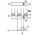
図4は、ガラス基板11の主表面に、前述で規定した短軸方向の長さが1.2μmの凹部(傷など)14のあるガラス基板を使ってフォトマスクを作製した場合を示す。通常フォトマスクは、ガラス基板11(図4(a))上に、遮光機能を有するクロム膜12を形成し(図4(b))、更にレジスト膜13を形成した後(図4(c))、このレジスト膜13に対して電子線露光及び現像を行って所望のレジストパターン13’を形成する(図4(d))。次に、このレジストパターン13’をマスクとして、例えば硝酸第2セリウムアンモニウムと過酸素塩とに純水を加えたエッチング液によってウェットエッチングを施して、クロム膜パターン12’を形成する(図4(e))。尚、このウェットエッチングは、通常クロム膜パターン12’の断面を垂直にするためにオーバーエッチングにするが、その際、クロム膜パターン12’が形成されている領域から形成されていない領域に跨った傷14がガラス基板11表面に存在すると、その傷14からエッチング液がクロム膜に浸透して図4(f)に示すようなクワレ15が発生してしまうという問題点があった。この長さ1.2μmの傷は、上述した問題だけでなく、それ以外にも様々な悪影響があるものと予想される。
FIG. 4 shows a case where a photomask is manufactured using a glass substrate having a concave portion (such as a scratch) 14 having a length of 1.2 μm in the minor axis direction defined above on the main surface of the
また、図5は、ガラス基板内部に脈理(透過率は同じで屈折率だけが違う欠陥)22のあるガラス基板21を使って位相シフトマスク(ハーフトーンマスク)を作製した場合を示す。位相シフトマスクは、図5(a)のガラス基板21上に、遮光機能と位相シフト機能を有するモリブデンシリサイド窒化(MoSiN)膜、レジスト膜を形成し、このレジスト膜に対して電子線露光及び現像を行って所望のレジストパターンを形成する(図示せず)。次に、このレジストパターンをマスクとして、例えばCF4とO2との混合ガスによるドライエッチングを施し、MoSiN膜パターン23を形成して位相シフトマスクを作製する(図5(b))。この得られた位相シフトマスクを使って半導体ウエハー等の被転写体にパターンを転写すると、図5(c)のようにガラス基板21の内部にある脈理22の影響で、被転写体上の光強度分布が異常な光強度分布24となり(25は脈理がない場合の正常な光強度分布)、所望なパターンが得られないという問題点があった。
FIG. 5 shows a case where a phase shift mask (halftone mask) is manufactured using a
また、従来の基板表面の微小な領域に光を集め、その反射出力、透過出力を比較して検査する、例えば特開昭58ー162038号公報に記載の面状態検査方法によって検査されたガラス基板を使用して、上述のフォトマスクや位相シフトマスクを作製した場合、検査では欠陥がないとされたガラス基板を使用しても、上述のようなクワレや、被転写体にパターンを転写すると所望なパターンが得られないという問題があった。これは、基板表面の傷といった検査光の進行方向に依存性をもった欠陥の場合、その傷がある一定方向の方向性を有しているので、検査光の入射方向によっては検出しないことが原因であり、また、基板内部の脈理といった欠陥の場合、従来の検査方法では反射出力がほとんど検出されないことが原因で、ガラス基板に欠陥がないと判別されたからである。 Further, a glass substrate inspected by a surface state inspection method described in, for example, Japanese Patent Application Laid-Open No. 58-162038, which collects light in a minute area on a conventional substrate surface and compares the reflected output and transmitted output for inspection. If the above photomask or phase shift mask is used to produce a photomask or phase shift mask as described above, it is desirable to transfer the pattern onto the transferred material as described above, even if a glass substrate that has been found to have no defects in the inspection is used. There was a problem that a simple pattern could not be obtained. This is because, in the case of a defect having a dependency on the traveling direction of the inspection light, such as a scratch on the substrate surface, since the scratch has a certain directionality, it may not be detected depending on the incident direction of the inspection light. This is because, in the case of defects such as striae inside the substrate, it is determined that there is no defect in the glass substrate because the reflected output is hardly detected by the conventional inspection method.
本発明は上記問題点を解決するためになされたものであり、高精度のパターニングや投影露光を可能にする電子デバイス用ガラス基板並びにこれを用いたフォトマスクブランク及びフォトマスクを提供することを目的とする。 The present invention has been made to solve the above-described problems, and an object of the present invention is to provide a glass substrate for an electronic device that enables high-precision patterning and projection exposure, and a photomask blank and a photomask using the same. And
なお、ここでいうフォトマスクブランク及びフォトマスクとは、クロム膜やMoSi膜などの遮光機能を有する遮光膜(パターン)を透明基板上に形成させたいわゆる通常のフォトマスクブランク及びフォトマスクを含むことは勿論、MoSiN膜やMoSiON膜などの遮光機能と位相シフト機能を有する位相シフト膜(パターン)を透明基板上に形成させた位相シフトマスクブランク及び位相シフトマスクを含むものである。 Note that the photomask blank and photomask referred to here include so-called ordinary photomask blanks and photomasks in which a light-shielding film (pattern) having a light-shielding function such as a chromium film or a MoSi film is formed on a transparent substrate. Of course, this includes a phase shift mask blank and a phase shift mask in which a phase shift film (pattern) having a light shielding function and a phase shift function, such as a MoSiN film or a MoSiON film, is formed on a transparent substrate.
上記目的を達成するために、本発明は以下の構成を有することを特徴とする。 In order to achieve the above object, the present invention has the following structure.
本発明の電子デバイス用ガラス基板は、
(構成1)検査光の光学的変化によって欠陥の有無を判別する方法においてある基準設定値に基づいて選別された電子デバイス用ガラス基板であって、前記ガラス基板に存在する欠陥は、前記検査光の進行方向に依存性を持たないものであることを特徴とするものである。
The glass substrate for electronic devices of the present invention is
(Configuration 1) A glass substrate for an electronic device selected based on a certain reference setting value in a method for determining the presence or absence of a defect by optical change of inspection light, and the defect present on the glass substrate is the inspection light It is characterized in that it has no dependency on the direction of travel.
従来のある一定方向の検査光を導入し、その反射出力、透過出力を比較して判別された基板の場合、基板表面の傷といった検査光の進行方向に依存性をもった欠陥を確実に除外することができない。即ち、傷に対し、一定方向の光しか通過しないから反射出力が全く検出されない場合もあるからである。それに対し、本発明者が先に出願した特願平9‐192763号記載の透光性物質の不均一性検査方法の場合、傷に対し、基板内部から表面に向かってあらゆる方向から光が照射されることになるので、検査光の進行方向に依存性をもった欠陥であっても除外することができる。したがって、本発明の電子デバイス用ガラス基板は、パターニングする際のエッチング等においてパターン欠陥が発生することがなく、高精度のパターニングが可能であり、また、このガラス基板を用いたフォトマスク、位相シフトマスクにより適切な露光が行える。 In the case of a substrate that has been discriminated by comparing conventional reflected light and transmitted output by introducing inspection light in a certain direction, defects that depend on the traveling direction of the inspection light, such as scratches on the substrate surface, are reliably excluded. Can not do it. That is, the reflected output may not be detected at all because only light in a certain direction passes through the scratch. On the other hand, in the case of the non-uniformity inspection method for translucent substances described in Japanese Patent Application No. 9-192863 previously filed by the present inventor, light is irradiated from all directions toward the surface from the inside of the substrate. Therefore, even a defect having dependency on the traveling direction of the inspection light can be excluded. Therefore, the glass substrate for an electronic device of the present invention can be patterned with high accuracy without causing pattern defects in etching or the like at the time of patterning. Also, a photomask and a phase shift using this glass substrate. Appropriate exposure can be performed by the mask.
ここで、光学的変化とは、例えば、光量の変化、光の進行方向の変化などある光学的特性が変化することをいう。また、基準設定値とは、電子デバイス用ガラス基板において許容できる欠陥(不均一性)に対応して得られる光の情報(画像情報、光量、輝度、強度分布等)をいい、使用者によって各自設定する閾値である。 Here, the optical change refers to a change in certain optical characteristics such as a change in the light amount and a change in the light traveling direction. The reference set value refers to light information (image information, light quantity, luminance, intensity distribution, etc.) obtained corresponding to an acceptable defect (non-uniformity) in the glass substrate for electronic devices. This is a threshold value to be set.
上記構成1の態様として、
(構成2)前記検査光は、前記ガラス基板の光路が光学的に均一の場合には、該ガラス基板の表面で全反射を繰り返して伝播するようにガラス基板内に光を導入したものであることを特徴とするものである。即ち、全反射条件を満足する光をガラス基板内に導入することにより、ガラス基板内の光路が光学的に均一の場合には、あらゆる方向からの光が基板全面及び基板内部の全部を埋め尽くすことになるので、例えば、ガラス基板表面にある特定な方向性をもった凹部(傷)があった場合や、ガラス基板内部に脈理といった欠陥があった場合でも、確実に且つ高精度、高速度に検出することが可能となる。具体的には、後述する構成8に規定する通りである。
As an aspect of the
(Configuration 2) When the optical path of the glass substrate is optically uniform, the inspection light is obtained by introducing light into the glass substrate so that the total reflection repeatedly propagates on the surface of the glass substrate. It is characterized by this. That is, by introducing light that satisfies the total reflection condition into the glass substrate, when the optical path in the glass substrate is optically uniform, light from all directions fills the entire surface of the substrate and the entire interior of the substrate. Therefore, for example, even when there is a recess (scratch) with a specific direction on the glass substrate surface or when there is a defect such as striae inside the glass substrate, it is reliable and highly accurate, It becomes possible to detect the speed. Specifically, it is as defined in Configuration 8 to be described later.
上記構成2の態様として、
(構成3)前記検査光はレーザー光であり、前記ガラス基板の表面は、少なくとも一組の互いに平行な主表面と、該主表面に直交する少なくとも一組の側面と、前記主表面及び前記側面によって挾まれた面取り面とを有するものであって、
前記ガラス基板内の光路が光学的に均一の場合には、該ガラス基板内を伝搬して前記主表面及び前記側面で全反射をし、かつ、少なくとも一組の側面の間で反復するように伝搬し、伝搬することによって、前記主表面、側面及び面取り面で囲まれる被検査領域にレーザー光が行き渡るように、レーザー光を導入するものであることを特徴とする。
As an aspect of the
(Configuration 3) The inspection light is laser light, and the surface of the glass substrate has at least one set of main surfaces parallel to each other, at least one set of side surfaces orthogonal to the main surfaces, the main surfaces, and the side surfaces. And a chamfered surface rubbed by
When the optical path in the glass substrate is optically uniform, it propagates in the glass substrate, totally reflects on the main surface and the side surface, and repeats between at least one pair of side surfaces. Propagating and propagating the laser beam so that the laser beam spreads over the region to be inspected surrounded by the main surface, the side surface, and the chamfered surface.
この場合、導入したレーザー光が、主表面、側面で全反射を繰り返してガラス基板内に実質的に閉じこめられた状態になり易く、実際上、ガラス基板の広範囲な領域での検査を同時に行なうことができ、高速検査が可能になるので好ましい。すなわち、,導入したレーザー光が全反射を繰り返す主表面への光の入射角は同じになり、また、側面に入射する光の入射角も同じで、それらが一定の関係(主表面における入射角をθとすると、側面に入射する光の入射角は90°−θになる)をもって伝搬するので、ガラス基板に入射してから最初に当たる主表面への入射角が、臨界角よりも大きくなるようにし、かつ、側面への入射角が臨界角よりも大きくなるように設定するだけで、実質的に光閉じ込めが成立するからである。具体的な検査光の導入の方法は、構成4に規定する通りである。 In this case, the introduced laser beam is likely to be substantially confined in the glass substrate by repeating total reflection on the main surface and side surfaces, and practically simultaneously inspecting a wide area of the glass substrate. This is preferable because high-speed inspection is possible. That is, the incident angle of light to the main surface where the introduced laser light repeats total reflection is the same, and the incident angle of light incident on the side surface is also the same, and they have a certain relationship (incident angle on the main surface). If θ is θ, the incident angle of the light incident on the side surface is 90 ° −θ), so that the incident angle on the main surface that first strikes after entering the glass substrate is larger than the critical angle. In addition, only by setting the incident angle to the side surface to be larger than the critical angle, optical confinement is substantially established. A specific method of introducing inspection light is as defined in Configuration 4.
構成3の態様として、
(構成4) 前記レーザー光は、前記面取り面から導入し、ガラス基板の光路が光学的に均一の場合には、前記面取り面からのみレーザー光が出射するように導入することを特徴とする。
As an aspect of
(Configuration 4) The laser light is introduced from the chamfered surface, and when the optical path of the glass substrate is optically uniform, the laser light is introduced so as to be emitted only from the chamfered surface.
また、本発明の電子デバイス用ガラス基板は、
(構成5)電子デバイス用ガラス基板であって、前記ガラス基板のパターンが形成される側の主表面に存在する凹部の大きさを、長軸方向の長さと、該長軸方向に対し垂直方向の短軸方向の長さで表したとき、前記凹部を主表面に対し垂直な断面で切ったときの主表面における短軸方向の長さが1μm以下であることを特徴とするものである。
Moreover, the glass substrate for electronic devices of the present invention is
(Structure 5) A glass substrate for an electronic device, wherein the size of the concave portion present on the main surface on the side where the pattern of the glass substrate is formed is determined so that the length in the major axis direction is perpendicular to the major axis direction. The length in the minor axis direction on the main surface when the recess is cut in a cross section perpendicular to the main surface is 1 μm or less.
電子デバイス用ガラス基板の主表面の凹部(傷などの表面欠陥)の大きさのうち、短軸方向の長さが1μm以下の小さなものでは、パターニングする際のエッチング等においてパターン欠陥が発生することがなく、高精度のパターニングが可能であり、また、このガラス基板を用いたフォトマスク、位相シフトマスクにより、適切な露光が行える。 Of the size of the recesses (surface defects such as scratches) on the main surface of the glass substrate for electronic devices, pattern defects occur in etching during patterning when the minor axis length is 1 μm or less. Therefore, high-precision patterning is possible, and appropriate exposure can be performed by a photomask and a phase shift mask using this glass substrate.
なお、ガラス基板表面に存在する凹部は、特願平9‐192763号記載の透光性物質の不均一性検査方法及び検査装置によって、短軸方向の長さが0.05μm程度の大きさを有する凹部でも確実に検出することができる。 The concave portion present on the surface of the glass substrate has a length in the minor axis direction of about 0.05 μm by a non-uniformity inspection method and inspection device for translucent substances described in Japanese Patent Application No. 9-192863. Even a concave portion having the same can be reliably detected.
上記構成5の好ましい態様として、
(構成6)前記凹部の短軸方向の長さが0.5μm以下であることを特徴とするものである。0.5μm以下とすることにより、パターニングする際のエッチング等において、パターン欠陥の発生を抑え、高精度のパターニングが可能となると共に、信頼性が向上する。
As a preferable aspect of the configuration 5,
(Configuration 6) The length of the concave portion in the minor axis direction is 0.5 μm or less. When the thickness is 0.5 μm or less, generation of pattern defects is suppressed in etching or the like during patterning, and high-accuracy patterning is possible, and reliability is improved.
上記構成5の更に好ましい態様として、
(構成7)前記凹部の短軸方向の長さが0.05〜0.25μmであることを特徴とするものである。凹部の短軸方向の長さを0.05μm未満とすると、品質上は勿論よいが、歩留まりが悪くなり、製造コストを上昇させることになるので好ましくない。
As a more preferable aspect of the configuration 5,
(Configuration 7) The length of the concave portion in the minor axis direction is 0.05 to 0.25 μm. If the length of the concave portion in the minor axis direction is less than 0.05 μm, the quality is of course good, but the yield deteriorates and the manufacturing cost increases, which is not preferable.
また、本発明の電子デバイス用ガラス基板は、
(構成8)電子デバイス用ガラス基板内部に、透過光に対する光学特性が不均一な部分が実質的に存在しないことを特徴とするものである。
Moreover, the glass substrate for electronic devices of the present invention is
(Structure 8) A portion where optical characteristics with respect to transmitted light are not uniform does not substantially exist inside a glass substrate for electronic devices.
透過光に対する光学特性が不均一な部分がガラス基板内部に実質的に存在しないとは、脈理や気泡等の不均一部分が存在しないか、あるいは、このガラス基板を用いたフォトマスク、位相シフトマスクによって露光を行っても、露光光の被転写体上での光強度分布が所定の許容範囲以内に収まる程度の極めて僅かな不均一性に過ぎないものをいい、特願平9―192763号記載の透光性物質の不均一性検査方法及び検査装置によって脈理等の不均一性が検出されないガラス基板ならば、全く問題なく適合する。 A portion where the optical characteristics with respect to the transmitted light are not substantially non-existent within the glass substrate means that there are no non-uniform portions such as striae or bubbles, or a photomask or phase shift using this glass substrate. Even if exposure is performed using a mask, the light intensity distribution of the exposure light on the transferred material is merely a very small non-uniformity within a predetermined allowable range. Japanese Patent Application No. 9-192863 Any glass substrate in which non-uniformity such as striae is not detected by the described non-uniformity inspection method and inspection apparatus of the translucent substance is suitable without any problem.
上記構成5〜7の態様として、
(構成9)前記電子デバイス用ガラス基板内部に、透過光に対する光学特性が不均一な部分が実質的に存在しないことを特徴とするものである。
As an aspect of the above configurations 5 to 7,
(Arrangement 9) The glass substrate for electronic devices is characterized in that there is substantially no portion having non-uniform optical characteristics with respect to transmitted light.
また、本発明のフォトマスクブランクは、
(構成10)前記構成1〜9記載の電子デバイス用ガラス基板の主表面上に、少なくとも遮光機能を有する薄膜が形成されていることを特徴とするものである。
The photomask blank of the present invention is
(Structure 10) A thin film having at least a light shielding function is formed on the main surface of the glass substrate for electronic devices according to the
また、本発明のフォトマスクは、
(構成11)前記構成1〜9の電子デバイス用ガラス基板の主表面上に、パターニングされた少なくとも遮光機能を有する薄膜パターンが形成されていることを特徴とするものである。
The photomask of the present invention is
(Structure 11) A patterned thin film pattern having at least a light shielding function is formed on the main surface of the glass substrate for electronic devices according to
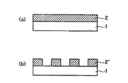
以下に本発明の実施の形態を図面を用いて説明する。図1(a)は本発明に係る電子デバイス用ガラス基板上にクロム膜が形成されたフォトマスクブランクの一実施形態を、図1(b)は本発明に係る電子デバイス用ガラス基板上にクロム膜パターンが形成されたフォトマスクの一実施形態をそれぞれ示す模式的な断面図である。 Embodiments of the present invention will be described below with reference to the drawings. FIG. 1A shows an embodiment of a photomask blank in which a chromium film is formed on a glass substrate for an electronic device according to the present invention, and FIG. 1B shows chromium on the glass substrate for an electronic device according to the present invention. It is typical sectional drawing which shows one Embodiment of the photomask in which the film | membrane pattern was formed, respectively.
図1(a)に示すように、フォトマスクブランクは、ガラス基板1と、ガラス基板1上に形成された遮光機能を有するクロム膜2とからなる。ガラス基板1は、基板主表面及び側面が精密研磨された、152.4mm×152.4mm×6.35mmの大きさの石英ガラス材料からなるものである。また、クロム膜2の膜厚は1000オングストロームである。ガラス基板1は、特願平9ー192763号の検査方法によって、ガラス基板1内部に脈理がないことを確認し、またガラス基板1表面に傷が存在することがわかったが、原子間力顕微鏡(AFM)で傷の大きさを確認したところ、その短軸方向の長さが1μmより大きな傷でないことが確認されたものである。
As shown to Fig.1 (a), the photomask blank consists of the
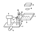
次に、特願平9―192763号の透光性物質の不均一性検査方法の一例を図3により簡単に説明する。図3は不均一性の検査装置であり、ガラス基板1の表面は、一組の互いに平行な主表面と、この主表面に直交する2組の側面と、主表面及び側面によって挾まれる面取り面とによって構成され、レーザー4からのレーザー光を、ミラー51、52で反射し、ガラス基板1の面取りした一辺A(面取り面)よりガラス基板1内に導入する。ミラー51、52にはガラス基板1に対する入射角度を調整するための入射角度調整手段53が設けられており、レーザー光がガラス基板1の表面(主表面及び側面)で全反射を起こす範囲内で入射角度を変動させて入射される。具体的には、ガラス基板1の面取りした一辺Aからレーザー光を導入し、導入したレーザー光が主表面及び側面で全反射を繰り返して(ガラス基板の光路が光学的に均一の場合に)、前記面取りした一辺A又は、前記一辺Aと同じ角度で面取りされた面からレーザー光が出射するように、ガラス基板1内に導入する。
Next, an example of the method for inspecting the non-uniformity of the translucent material of Japanese Patent Application No. 9-192863 will be briefly described with reference to FIG. FIG. 3 shows a non-uniformity inspection apparatus, in which the surface of the
ガラス基板1内に入射したレーザー光は、ガラス基板1の主表面及び側面で全反射を繰り返し、一組の側面の間で違う経路又は同じ経路を通って反復しながら、ガラス基板1の一辺Bに沿った一平面状(薄板状)の領域内にほぼ閉じ込められたような状態で伝播する。この工程を、駆動装置6によってテーブル7と共にレーザー4、ミラー51、52等をガラス基板1の一辺Aに沿って順次移動させて実施し、ガラス基板1内の全領域にもれなくレーザー光を伝播させる。
The laser light incident on the
ガラス基板1表面に傷等の不均一部分があったり、ガラス基板1内部に脈理等の不均一部分があったりすると、傷や屈折率の違うところで、レーザー光は本来均一ならば通る光路(経路)をはずれ、ガラス基板1表面での全反射条件が満足されなくなり、ガラス基板1の主表面からレーザー光が漏れ出す。この漏れ出したレーザー光をレンズ系8でCCD9に結像して検出する。このように、物理的な臨界現象である全反射を利用しているため、ガラス基板1の不均一部分と均一部分における検査光に対する応答も臨界的となり、不均一性が非常にはっきりとしたコントラストで現れ、微小な傷等の不均一を高感度で検出できる。更に、ガラス基板1表面の不均一のみならず、内部の脈理等の欠陥も検出できる。
If there is a non-uniform part such as a scratch on the surface of the
図1(b)に示すフォトマスクは、図1(a)のフォトマスクブランク上にレジスト膜を形成し、このレジスト膜に対して電子線露光及び現像を行って所望のレジストパターンを形成し、次に、このレジストパターンをマスクとして硝酸第2セリウムアンモニウム165gと濃度70%の過酸素塩42mlとに純水を加えて1000mlとしたエッチング液を温度19℃〜20℃に保持し、このエッチング液によってウェットエッチングを施してクロム膜パターン2’を形成したものである。
In the photomask shown in FIG. 1B, a resist film is formed on the photomask blank of FIG. 1A, and the resist film is subjected to electron beam exposure and development to form a desired resist pattern. Next, using this resist pattern as a mask, 165 g of ceric ammonium nitrate and 42 ml of a 70% concentration of peroxygen salt are added to pure water to maintain a 1000 ml etching solution at a temperature of 19 ° C. to 20 ° C. The
また、図2(a)に示す位相シフトマスクブランクは、ガラス基板1と、遮光機能、位相シフト機能を有するMoSiN(Mo:13at%、Si:40at%、N:47at%の組成で、屈折率が2.34、波長248nmにおける光透過率が5%、位相シフト量が180°)のハーフトーン膜3とからなる。ガラス基板1は、基板主表面及び側面が精密研磨された、152.4mm×152.4mm×6.35mmの大きさの石英ガラス材料からなるものである。このガラス基板1は図3の検査方法によって、ガラス基板内部に脈理がないことを確認し、さらに、ガラス基板表面に傷が存在していることがわかったが、その傷を原子間力顕微鏡(AFM)で大きさを確認したところ、短軸方向の長さが1μmの傷であることが確認されたものである。またMoSiNのハーフトーン膜3の膜厚は925オングストロームである。
Further, the phase shift mask blank shown in FIG. 2A has a
図2(b)の位相シフトマスクは、図2(a)の位相シフトマスクブランク上にレジスト膜を形成し、このレジスト膜に対して電子線露光及び現像を行って所望のレジストパターンを形成し、次に、このレジストパターンをマスクとしてCF4とO2 との混合ガスによるドライエッチングによって、MoSiN膜パターン3’を形成したものである。 In the phase shift mask of FIG. 2B, a resist film is formed on the phase shift mask blank of FIG. 2A, and the resist film is subjected to electron beam exposure and development to form a desired resist pattern. Then, using this resist pattern as a mask, a MoSiN film pattern 3 'is formed by dry etching using a mixed gas of CF4 and O2.
これらのフォトマスク、位相シフトマスクは、丁度発見した傷が、各パターンが形成されない領域から形成された領域にまたがって存在していたが、それぞれのパターンを検査したところ、クワレ等の欠陥がなく、所望のパターンが形成されていることを確認した。また、これらのフォトマスク、位相シフトマスクによって被転写物にパターンを転写したが、パターン転写も良好であった。 In these photomasks and phase shift masks, the scratches that were just found existed over the area formed from the area where each pattern was not formed, but when each pattern was inspected, there were no defects such as quarrels. It was confirmed that a desired pattern was formed. Moreover, although the pattern was transferred to the transfer object using these photomask and phase shift mask, the pattern transfer was also good.
なお、上記実施形態と同様の152.4mm×152.4mm×6.35mmの大きさの石英ガラス基板の主表面及び側面を精密研磨したものを3枚用意し、これらガラス基板を、図3に示す検査方法によってガラス基板主表面の不均一性を検査した。その検査結果を上記と同様の評価方法により大きさを確認したところ、ある領域において、短軸方向の長さが0.5μm、0.3μm、0.1μmの傷があることが確認された。このガラス基板に上記実施形態と同様の膜を成膜し、パターニングして位相シフトマスクを得た。これらの位相シフトマスクによって被転写物にパターンを転写したが、パターン転写も良好であり、上記1μmの傷の場合と比較して、パターン形成の信頼性を向上できる。 Three quartz glass substrates having a size of 152.4 mm × 152.4 mm × 6.35 mm, which are the same as those in the above-described embodiment, are prepared by polishing the main surface and side surfaces, and these glass substrates are shown in FIG. The non-uniformity of the main surface of the glass substrate was inspected by the inspection method shown. When the size of the inspection result was confirmed by the same evaluation method as described above, it was confirmed that there was a scratch having lengths in the minor axis direction of 0.5 μm, 0.3 μm, and 0.1 μm in a certain region. A film similar to that of the above embodiment was formed on this glass substrate and patterned to obtain a phase shift mask. Although the pattern was transferred to the transfer object using these phase shift masks, the pattern transfer was also good, and the reliability of pattern formation could be improved compared to the case of the 1 μm scratch.
次に、上記実施形態と比較するための比較例を述べる。ガラス基板を基板主表面及び側面を精密研磨し、152.4mm×152.4mm×6.35mmの大きさの石英ガラス基板を得た。このガラス基板を、図3に示す検査方法によって、ガラス基板主表面の不均一性を検査したところ、ある領域において基板主表面に短軸方向の長さが2μmの傷があることが確認された(傷の長さは原子間力顕微鏡(AFM)で測定した)。なお、この傷は、基板の研磨工程の際、望ましくない異物などが混入されたことにより、異物が通った軌跡によって形成されたものと思われる。このガラス基板を使用し、上述の実施形態と同様にしてフォトマスク、位相シフトマスクをそれぞれ作製した。この得られたフォトマスクのパターンを確認したところ、クワレが発生していた。 Next, a comparative example for comparison with the above embodiment will be described. The glass substrate was precisely polished on the substrate main surface and side surfaces to obtain a quartz glass substrate having a size of 152.4 mm × 152.4 mm × 6.35 mm. When this glass substrate was inspected for non-uniformity on the main surface of the glass substrate by the inspection method shown in FIG. 3, it was confirmed that there was a scratch having a length in the minor axis direction of 2 μm on the main surface of the substrate in a certain region. (The length of the wound was measured with an atomic force microscope (AFM)). This scratch is considered to have been formed by a trajectory through which foreign matter has passed due to the inclusion of undesirable foreign matter or the like during the polishing process of the substrate. Using this glass substrate, a photomask and a phase shift mask were respectively produced in the same manner as in the above embodiment. When the pattern of the obtained photomask was confirmed, a crease was generated.
また、図3の検査方法によってガラス基板内部の不均一性を検査したところ、ある領域において、図6に示すような輝点が球状に集まった画像30が検出され、ガラス基板内部に脈理が存在していることが確認された。尚、この脈理は、光学顕微鏡では確認することはできなかった。このガラス基板を使用し、上述の実施形態と同様にして位相シフトマスクを作製した。この得られた位相シフトマスクを用いて、半導体ウエハーにパターンを転写したところ、線幅から飛びだしたパターンが確認された。これは、ガラス基板内部に存在する脈理の影響で、半導体ウェハ上の光強度分布が設計値から外れ、異常な光強度分布のまま転写されてしまったからである。
Further, when the non-uniformity inside the glass substrate was inspected by the inspection method of FIG. 3, an
次に、他の実施形態について説明する。ガラス基板を基板主表面及び側面を精密研磨し、152.4mm×152.4mm×6.35mmの大きさの石英ガラス基板を得た。このガラス基板を、図3に示す検査方法によって、ガラス基板主表面の不均一性を検査し、良品、不良品を選別した。具体的には、予めガラス基板に存在する不均一性の種類(表面部の傷やクラック、内部の脈理や異物など)や、大きさ(面積、長さ、幅、深さ、領域など)に対して、表面から漏出する光の情報(漏出光の光量、輝度、強度分布、表面からの深さ)の関係(情報)をコンピューター等に蓄積しておき、不均一性の許容範囲に対応した光の情報(基準設定値)と、検査によって検出した光の情報とを比較し、検出した光の情報が、基準設定値を満足しているものを選んだ。この選ばれたガラス基板を使用し、上述の実施形態と同様にしてフォトマスクを作製した。この得られたフォトマスクのパターンを確認したところ、クワレ等の欠陥がなく、所望のパターンが形成されていることを確認した。また、これらのフォトマスク、位相シフトマスクによって被転写物にパターンを転写したが、パターン転写も良好であった。 Next, another embodiment will be described. The glass substrate was precisely polished on the substrate main surface and side surfaces to obtain a quartz glass substrate having a size of 152.4 mm × 152.4 mm × 6.35 mm. The glass substrate was inspected for non-uniformity on the main surface of the glass substrate by the inspection method shown in FIG. Specifically, the type of non-uniformity (surface scratches and cracks, internal striae, foreign matter, etc.) and size (area, length, width, depth, region, etc.) pre-existing on the glass substrate in advance On the other hand, the relationship (information) of light leaking from the surface (the amount of light leaked, brightness, intensity distribution, depth from the surface) is stored in a computer, etc., and the nonuniformity tolerance is accommodated. The light information (reference setting value) and the light information detected by the inspection were compared, and the detected light information satisfied the reference setting value. Using this selected glass substrate, a photomask was produced in the same manner as in the above embodiment. When the pattern of the obtained photomask was confirmed, it was confirmed that there was no defect such as quarrel and a desired pattern was formed. Moreover, although the pattern was transferred to the transfer object using these photomask and phase shift mask, the pattern transfer was also good.
次に、上記実施形態と比較するための比較例を述べる。ガラス基板を基板主表面及び側面を精密研磨し、152.4mm×152.4mm×6.35mmの大きさの石英ガラス基板を得た。このガラス基板表面の微小な領域に光を集め、その反射出力、透過出力を比較して検査する、例えば特開昭58‐162038号公報に記載の面状態検査方法で検査し、良品、不良品を選別した。具体的には、透過出力、反射出力を比較し、反射出力がある基準設定値以下であるものを選んだ。このガラス基板を使用し、上述の実施形態と同様にしてフォトマスクを作製した。この得られたフォトマスクのパターンを確認したところ、クワレが発生していた。なお、この良品として選ばれたガラス基板を、図3に示す検査方法によって検査したところ、ガラス基板表面のある領域から漏出した光(欠陥)を検出し、その光が予め設定しておいた基準設定値を越えたものであることを確認した。これは、比較例のガラス基板は、基板表面の傷といった検査光の進行方向に依存性をもった欠陥が含まれているのに対し、実施形態のガラス基板は、検査光の進行方向に依存性をもった欠陥が全く含まれていないからである。 Next, a comparative example for comparison with the above embodiment will be described. The glass substrate was precisely polished on the substrate main surface and side surfaces to obtain a quartz glass substrate having a size of 152.4 mm × 152.4 mm × 6.35 mm. Light is collected in a small area on the surface of the glass substrate, and the reflected output and transmitted output are compared and inspected. For example, the surface state inspection method described in Japanese Patent Application Laid-Open No. 58-162038 is used for inspection. Sorted out. Specifically, the transmission output and the reflection output were compared, and the output whose reflection output was below a certain reference set value was selected. Using this glass substrate, a photomask was produced in the same manner as in the above embodiment. When the pattern of the obtained photomask was confirmed, a crease was generated. When the glass substrate selected as a non-defective product was inspected by the inspection method shown in FIG. 3, light (defect) leaked from a certain area on the surface of the glass substrate was detected, and the light was set in advance. It was confirmed that the set value was exceeded. This is because the glass substrate of the comparative example includes defects that depend on the traveling direction of the inspection light, such as scratches on the substrate surface, whereas the glass substrate of the embodiment depends on the traveling direction of the inspection light. This is because it does not contain any defects that have sex.
以上、実施形態を挙げて本発明を説明したが、本発明は上記実施形態に限定されるものではない。例えば、ガラス基板は電子デバイス用ガラス基板を挙げたが、これに限定されず、情報記録媒体用ガラス基板(磁気ディスクや光ディスク)、液晶(ディスプレイ)用ガラス基板にも適用できる。 While the present invention has been described with reference to the embodiment, the present invention is not limited to the above embodiment. For example, the glass substrate is a glass substrate for electronic devices, but is not limited thereto, and can be applied to a glass substrate for information recording media (magnetic disk or optical disk) and a glass substrate for liquid crystal (display).
また、例えば、遮光膜は、クロムに限定されず、例えば、クロムと、酸素、窒素、炭素のうちから選ばれる少なくとも一種とを含む材料や、アルミニウム、モリブデンシリサイド(MoSi)等の膜や、あるいはこれらに酸素、窒素、炭素のうちから選ばれる少なくとも一種を含ませた材料からなるものであってもよい。また、1層だけでなく、2層以上形成されたものであってもよい。 Further, for example, the light-shielding film is not limited to chromium, and for example, a material containing chromium and at least one selected from oxygen, nitrogen, and carbon, a film of aluminum, molybdenum silicide (MoSi), or the like These may be made of a material containing at least one selected from oxygen, nitrogen, and carbon. Moreover, not only one layer but two or more layers may be formed.
また、半透光膜(ハーフトーン膜)は、モリブデン、シリコン、窒素からなるものに限定されず、例えば、モリブデンとシリコンと酸素、モリブデンとシリコンと酸素と窒素とからなる半透光膜や、タングステン、チタン、タンタル、クロムから選ばれる金属とシリコンと酸素及び/又は窒素とからなる半透光膜であってもよい。 Further, the semi-transparent film (halftone film) is not limited to one made of molybdenum, silicon, and nitrogen. For example, a semi-transparent film made of molybdenum, silicon, and oxygen, molybdenum, silicon, oxygen, and nitrogen, It may be a semi-transparent film made of a metal selected from tungsten, titanium, tantalum, and chromium, silicon, and oxygen and / or nitrogen.
また、位相シフトマスクとしては、実施形態に挙げたハーフトーンマスクに限らず、遮光膜パターン間に、位相シフト機能を有する膜(例えば、SiO2
)が形成されたレベンソン型位相シフトマスクのものや、SOG膜が形成された2層以上の位相シフト機能を有する膜が形成された位相シフトマスクであってもよい。
Further, the phase shift mask is not limited to the halftone mask described in the embodiment, but a film having a phase shift function (for example, SiO 2) between the light shielding film patterns.
Or a phase shift mask on which a film having a phase shift function of two or more layers on which an SOG film is formed is formed.
以上要するに、本発明によれば、電子デバイス用ガラス基板の主表面の凹部(傷などの表面欠陥)の大きさを、長軸方向の長さと、長軸方向に対し垂直方向の短軸方向の長さで表したとき、この凹部を主表面に対し垂直な断面で切ったときの主表面における短軸方向の長さが1μm以下としたため、パターニング時のエッチング等においてパターン欠陥が発生することがなく、高精度のパターニングが可能である。また、電子デバイス用ガラス基板内部に、透過光に対する光学特性が不均一な部分が実質的に存在しないため、このガラス基板を用いたフォトマスク、位相シフトマスクにより適正な露光が行える。 In short, according to the present invention, the size of the recesses (surface defects such as scratches) on the main surface of the glass substrate for electronic devices can be set to the length in the major axis direction and the minor axis direction perpendicular to the major axis direction. When expressed in length, the length in the minor axis direction on the main surface when this recess is cut in a cross section perpendicular to the main surface is set to 1 μm or less, and pattern defects may occur during etching during patterning. And high-precision patterning is possible. Further, since there is substantially no non-uniform optical property with respect to transmitted light inside the glass substrate for electronic devices, appropriate exposure can be performed with a photomask or phase shift mask using this glass substrate.
また、検査光の光学的変化によって欠陥の有無を判別する方法においてある基準設定値で選別された電子デバイス用ガラス基板であって、前記ガラス基板に存在する欠陥が、前記検査光の進行方向に依存性を持たないものであるので、パターニング時のエッチング等においてパターン欠陥が発生することがなく、高精度のパターニングが可能であるとともに、このガラス基板を用いたフォトマスク、位相シフトマスクにより適正な露光が行える。 Further, in the glass substrate for electronic devices selected by a reference set value in a method for determining the presence or absence of a defect by optical change of inspection light, the defect present on the glass substrate is in the traveling direction of the inspection light. Since there is no dependency, pattern defects do not occur during patterning etching and the like, and high-precision patterning is possible, and a photomask and phase shift mask using this glass substrate are suitable. Exposure is possible.
1 ガラス基板
2 クロム膜
2’クロム膜パターン
3 MoSiNのハーフトーン膜
3’MoSiN膜パターン
4 レーザー
51、52 ミラー
53入射角度調整手段
6 駆動装置
7 テーブル
8 レンズ系
9 CCD
14 傷
22 脈理
DESCRIPTION OF
14
Claims (4)
前記精密研磨されたガラス基板を、検査光の光学的変化によって欠陥の有無を判別する検査方法によって検査し、基準設定値を満足しているものを選ぶ検査工程とを有する電子デバイス用ガラス基板の製造方法であって、
前記検査工程における検査方法は、検査光としてレーザー光を用い、前記ガラス基板内の光路が光学的に均一の場合には、該ガラス基板内を伝搬して前記主表面及び前記側面で全反射をし、かつ、少なくとも一組の側面の間で反復するように伝搬し、伝搬することによって、前記主表面、側面及び面取り面で囲まれる被検査領域に前記レーザー光が行き渡るように、前記レーザー光を前記ガラス基板に導入し、前記ガラス基板内の光路に光学的に不均一な部分がある場合に表面から漏出する光の情報を求めて基準設定値と比較する方法であり、
前記光の情報は、CCDを用いて検出された画像情報、光量、輝度、強度分布、及び表面からの深さのうち少なくとも一つの情報であり、
前記電子デバイス用ガラス基板は、その主表面に遮光機能を有する薄膜を形成してフォトマスクブランクを製造する際に用いられるものであり、
前記フォトマスクブランクは位相シフトマスクブランクであり、
前記検査工程における基準設定値は、前記電子デバイス用ガラス基板を用いて製造したフォトマスクブランクの薄膜に所定のパターンを形成してフォトマスクを製造し、そのフォトマスクを用いてパターン転写したときに、前記電子デバイス用ガラス基板内部の不均一部分に起因して前記転写パターンにパターン不良が発生しないような値を選定して設定し、
前記レーザー光を、前記面取り面から導入し、かつ、前記ガラス基板の光路が光学的に均一の場合には、前記面取り面からのみレーザー光が出射するように導入し、
前記レーザー光の導入は、前記ガラス基板に入射してから最初に当たる前記主表面への入射角が、臨界角よりも大きくなるようにし、かつ、前記側面への入射角が臨界角よりも大きくなるように設定することを特徴とする電子デバイス用ガラス基板の製造方法。 A glass substrate having at least one set of main surfaces parallel to each other, at least one set of side surfaces orthogonal to the main surfaces, and a chamfered surface sandwiched between the main surfaces and the side surfaces, the main surfaces and the side surfaces Preparing a precision polished glass substrate,
Inspecting the precision-polished glass substrate by an inspection method for determining the presence or absence of a defect by optical change of inspection light, and selecting a glass substrate for an electronic device that satisfies a reference set value A manufacturing method comprising:
The inspection method in the inspection step uses laser light as inspection light, and when the optical path in the glass substrate is optically uniform, propagates in the glass substrate and totally reflects on the main surface and the side surface. And the laser beam is propagated in a repetitive manner between at least one pair of side surfaces so that the laser beam is distributed over the region to be inspected surrounded by the main surface, the side surface, and the chamfered surface. Is introduced into the glass substrate, and when there is an optically non-uniform portion in the optical path in the glass substrate, information on the light leaking from the surface is obtained and compared with a reference set value,
The light information is at least one of image information detected using a CCD , light quantity, luminance, intensity distribution, and depth from the surface,
The glass substrate for electronic devices is used when manufacturing a photomask blank by forming a thin film having a light shielding function on the main surface thereof,
The photomask blank is a phase shift mask blank;
The reference set value in the inspection step is that when a predetermined pattern is formed on a thin film of a photomask blank manufactured using the glass substrate for electronic devices, a photomask is manufactured, and the pattern is transferred using the photomask. , Select and set a value that does not cause pattern defects in the transfer pattern due to non-uniform portions inside the glass substrate for electronic devices,
When the laser beam is introduced from the chamfered surface and the optical path of the glass substrate is optically uniform, introduced so that the laser beam is emitted only from the chamfered surface,
The introduction of the laser beam is such that the incident angle to the main surface that first strikes after entering the glass substrate is larger than the critical angle, and the incident angle to the side surface is larger than the critical angle. The manufacturing method of the glass substrate for electronic devices characterized by setting as follows.
前記精密研磨されたガラス基板を、検査光の光学的変化によって欠陥の有無を判別する検査方法によって検査し、基準設定値を満足しているものを選ぶ検査工程とを有する電子デバイス用ガラス基板の製造方法であって、
前記検査工程における検査方法は、検査光としてレーザー光を用い、前記ガラス基板内の光路が光学的に均一の場合には、該ガラス基板内を伝搬して前記主表面及び前記側面で全反射をし、かつ、少なくとも一組の側面の間で反復するように伝搬し、伝搬することによって、前記主表面、側面及び面取り面で囲まれる被検査領域に前記レーザー光が行き渡るように、前記レーザー光を前記ガラス基板に導入し、前記ガラス基板内の光路に光学的に不均一な部分がある場合に表面から漏出する光の情報を求めて基準設定値と比較する方法であり、
前記光の情報は、CCDを用いて検出された画像情報、光量、輝度、強度分布、及び表面からの深さのうち少なくとも一つの情報であり、
前記電子デバイス用ガラス基板は、その主表面に遮光機能を有する薄膜を形成してフォトマスクブランクを製造する際に用いられるものであり、
前記検査工程における基準設定値は、前記電子デバイス用ガラス基板を用いて製造したフォトマスクブランクの薄膜にウエットエッチングにより所定のパターンを形成する際、このパターンにパターン欠陥が生じないような値を選定して設定し、
前記レーザー光を、前記面取り面から導入し、かつ、前記ガラス基板の光路が光学的に均一の場合には、前記面取り面からのみレーザー光が出射するように導入し、
前記レーザー光の導入は、前記ガラス基板に入射してから最初に当たる前記主表面への入射角が、臨界角よりも大きくなるようにし、かつ、前記側面への入射角が臨界角よりも大きくなるように設定することを特徴とする電子デバイス用ガラス基板の製造方法。 A glass substrate having at least one set of main surfaces parallel to each other, at least one set of side surfaces orthogonal to the main surfaces, and a chamfered surface sandwiched between the main surfaces and the side surfaces, the main surfaces and the side surfaces Preparing a precision polished glass substrate,
Inspecting the precision-polished glass substrate by an inspection method for determining the presence or absence of a defect by optical change of inspection light, and selecting a glass substrate for an electronic device that satisfies a reference set value A manufacturing method comprising:
The inspection method in the inspection step uses laser light as inspection light, and when the optical path in the glass substrate is optically uniform, propagates in the glass substrate and totally reflects on the main surface and the side surface. And the laser beam is propagated in a repetitive manner between at least one pair of side surfaces so that the laser beam is distributed over the region to be inspected surrounded by the main surface, the side surface, and the chamfered surface. Is introduced into the glass substrate, and when there is an optically uneven portion in the optical path in the glass substrate, information on light leaking from the surface is obtained and compared with a reference set value,
The light information is at least one of image information detected using a CCD , light quantity, luminance, intensity distribution, and depth from the surface,
The glass substrate for electronic devices is used when producing a photomask blank by forming a thin film having a light shielding function on the main surface thereof,
The reference set value in the inspection process is selected such that when a predetermined pattern is formed by wet etching on a thin film of a photomask blank manufactured using the glass substrate for electronic devices, a pattern defect does not occur in the pattern. Set
When the laser beam is introduced from the chamfered surface and the optical path of the glass substrate is optically uniform, introduced so that the laser beam is emitted only from the chamfered surface,
The introduction of the laser beam is such that the incident angle to the main surface that first strikes after entering the glass substrate is larger than the critical angle, and the incident angle to the side surface is larger than the critical angle. The manufacturing method of the glass substrate for electronic devices characterized by setting as follows.
Priority Applications (1)
| Application Number | Priority Date | Filing Date | Title |
|---|---|---|---|
| JP2004212026A JP4100514B2 (en) | 1997-12-26 | 2004-07-20 | Manufacturing method of glass substrate for electronic device, manufacturing method of photomask blank, and manufacturing method of photomask |
Applications Claiming Priority (2)
| Application Number | Priority Date | Filing Date | Title |
|---|---|---|---|
| JP36883697 | 1997-12-26 | ||
| JP2004212026A JP4100514B2 (en) | 1997-12-26 | 2004-07-20 | Manufacturing method of glass substrate for electronic device, manufacturing method of photomask blank, and manufacturing method of photomask |
Related Parent Applications (1)
| Application Number | Title | Priority Date | Filing Date |
|---|---|---|---|
| JP37043298A Division JPH11264798A (en) | 1997-12-26 | 1998-12-25 | Glass board for electronic device and photo-mask blank using it, and photo-mask |
Publications (2)
| Publication Number | Publication Date |
|---|---|
| JP2005031689A JP2005031689A (en) | 2005-02-03 |
| JP4100514B2 true JP4100514B2 (en) | 2008-06-11 |
Family
ID=34219719
Family Applications (1)
| Application Number | Title | Priority Date | Filing Date |
|---|---|---|---|
| JP2004212026A Expired - Fee Related JP4100514B2 (en) | 1997-12-26 | 2004-07-20 | Manufacturing method of glass substrate for electronic device, manufacturing method of photomask blank, and manufacturing method of photomask |
Country Status (1)
| Country | Link |
|---|---|
| JP (1) | JP4100514B2 (en) |
Families Citing this family (4)
| Publication number | Priority date | Publication date | Assignee | Title |
|---|---|---|---|---|
| JP4859436B2 (en) * | 2005-10-18 | 2012-01-25 | Hoya株式会社 | Manufacturing method of glass substrate for mask blank, manufacturing method of mask blank, manufacturing method of mask for exposure, and manufacturing method of glass member for lithography |
| JP6165535B2 (en) * | 2012-08-24 | 2017-07-19 | Hoya株式会社 | Mask blank substrate manufacturing method, mask blank manufacturing method, transfer mask manufacturing method, semiconductor device manufacturing method, and inspection apparatus |
| JP7154572B2 (en) * | 2018-09-12 | 2022-10-18 | Hoya株式会社 | MASK BLANK, TRANSFER MASK, AND METHOD FOR MANUFACTURING SEMICONDUCTOR DEVICE |
| JP7546823B2 (en) * | 2019-11-15 | 2024-09-09 | 義晴 加藤 | Electronic component inspection device and electronic component inspection method |
-
2004
- 2004-07-20 JP JP2004212026A patent/JP4100514B2/en not_active Expired - Fee Related
Also Published As
| Publication number | Publication date |
|---|---|
| JP2005031689A (en) | 2005-02-03 |
Similar Documents
| Publication | Publication Date | Title |
|---|---|---|
| KR101018567B1 (en) | Gray tone mask blank, gray tone mask and production method therefor, and production method for liquid crystal display device | |
| KR960006817B1 (en) | Mask for manufacturing semiconductor device and the method of manufacture thereof | |
| US20070065732A1 (en) | Photomask providing uniform critical dimension on semiconductor device and method of manufacturing the same | |
| US5439767A (en) | Phase shift mask and its inspection method | |
| KR100532641B1 (en) | Mask substrate and its manufacturing method | |
| JP3080024B2 (en) | Exposure method and method of measuring spherical aberration | |
| JP4100514B2 (en) | Manufacturing method of glass substrate for electronic device, manufacturing method of photomask blank, and manufacturing method of photomask | |
| US6555273B2 (en) | Glass substrate for an electron device, photomask blank and photomask using the same | |
| JPH05142754A (en) | Inspecting method for phase shift mask | |
| JPH11264798A (en) | Glass board for electronic device and photo-mask blank using it, and photo-mask | |
| JP2006251611A (en) | Self alignment type phase shift mask and a method for manufacturing the same | |
| JPH06250376A (en) | Phase shift mask and production of phase shift mask | |
| JP5028437B2 (en) | Manufacturing method of glass substrate for mask blank, manufacturing method of mask blank, and manufacturing method of photomask for exposure | |
| US20090233189A1 (en) | Device and method for obtaining exposure correction information, and manufacturing method of semiconductor device | |
| JP2991661B2 (en) | Semiconductor device process defect inspection method | |
| JPH08194303A (en) | Phase shift mask and its production | |
| JP5090379B2 (en) | Manufacturing method of glass substrate for mask blank, manufacturing method of mask blank, and manufacturing method of photomask for exposure | |
| JP2018189997A (en) | Photomask substrate, photomask blank, photomask, production method of photomask substrate, production method of display device, handling method of photomask, and handling method of photomask substrate | |
| JP2000162757A (en) | Production of phase shift mask | |
| JP3422054B2 (en) | Optical mask and method of manufacturing the same | |
| JP2001228598A (en) | Mask blank for phase shift mask of substrate mortise type, phase shift mask of substrate mortise type and method for manufacturing phase shift mask of substrate mortise type | |
| US7387965B2 (en) | Reference pattern for creating a defect recognition level, method of fabricating the same and method of inspecting defects using the same | |
| JPH06282064A (en) | Production of phase shift mask with auxiliary pattern | |
| KR20190013517A (en) | Method for inspecting a photomask, method for manufacturing a photomask, and apparatus for inspecting a photomask | |
| JPH045657A (en) | Method for measuring and inspecting thickness of phase shift film of phase shift mask, production of phase shift mask and method for inspecting defect of phase shift mask |
Legal Events
| Date | Code | Title | Description |
|---|---|---|---|
| A977 | Report on retrieval |
Free format text: JAPANESE INTERMEDIATE CODE: A971007 Effective date: 20060802 |
|
| A131 | Notification of reasons for refusal |
Free format text: JAPANESE INTERMEDIATE CODE: A131 Effective date: 20070830 |
|
| A521 | Written amendment |
Free format text: JAPANESE INTERMEDIATE CODE: A523 Effective date: 20071029 |
|
| A131 | Notification of reasons for refusal |
Free format text: JAPANESE INTERMEDIATE CODE: A131 Effective date: 20071122 |
|
| A521 | Written amendment |
Free format text: JAPANESE INTERMEDIATE CODE: A523 Effective date: 20080121 |
|
| TRDD | Decision of grant or rejection written | ||
| A01 | Written decision to grant a patent or to grant a registration (utility model) |
Free format text: JAPANESE INTERMEDIATE CODE: A01 Effective date: 20080312 |
|
| A61 | First payment of annual fees (during grant procedure) |
Free format text: JAPANESE INTERMEDIATE CODE: A61 Effective date: 20080312 |
|
| FPAY | Renewal fee payment (event date is renewal date of database) |
Free format text: PAYMENT UNTIL: 20110328 Year of fee payment: 3 |
|
| R150 | Certificate of patent or registration of utility model |
Free format text: JAPANESE INTERMEDIATE CODE: R150 |
|
| FPAY | Renewal fee payment (event date is renewal date of database) |
Free format text: PAYMENT UNTIL: 20110328 Year of fee payment: 3 |
|
| FPAY | Renewal fee payment (event date is renewal date of database) |
Free format text: PAYMENT UNTIL: 20120328 Year of fee payment: 4 |
|
| FPAY | Renewal fee payment (event date is renewal date of database) |
Free format text: PAYMENT UNTIL: 20120328 Year of fee payment: 4 |
|
| FPAY | Renewal fee payment (event date is renewal date of database) |
Free format text: PAYMENT UNTIL: 20130328 Year of fee payment: 5 |
|
| FPAY | Renewal fee payment (event date is renewal date of database) |
Free format text: PAYMENT UNTIL: 20130328 Year of fee payment: 5 |
|
| FPAY | Renewal fee payment (event date is renewal date of database) |
Free format text: PAYMENT UNTIL: 20140328 Year of fee payment: 6 |
|
| R250 | Receipt of annual fees |
Free format text: JAPANESE INTERMEDIATE CODE: R250 |
|
| R250 | Receipt of annual fees |
Free format text: JAPANESE INTERMEDIATE CODE: R250 |
|
| R250 | Receipt of annual fees |
Free format text: JAPANESE INTERMEDIATE CODE: R250 |
|
| R250 | Receipt of annual fees |
Free format text: JAPANESE INTERMEDIATE CODE: R250 |
|
| LAPS | Cancellation because of no payment of annual fees |