JP4067897B2 - Memory device with reduced read time - Google Patents
Memory device with reduced read time Download PDFInfo
- Publication number
- JP4067897B2 JP4067897B2 JP2002207874A JP2002207874A JP4067897B2 JP 4067897 B2 JP4067897 B2 JP 4067897B2 JP 2002207874 A JP2002207874 A JP 2002207874A JP 2002207874 A JP2002207874 A JP 2002207874A JP 4067897 B2 JP4067897 B2 JP 4067897B2
- Authority
- JP
- Japan
- Prior art keywords
- switch
- memory cell
- bit line
- read
- memory
- Prior art date
- Legal status (The legal status is an assumption and is not a legal conclusion. Google has not performed a legal analysis and makes no representation as to the accuracy of the status listed.)
- Expired - Fee Related
Links
- 238000000034 method Methods 0.000 claims description 21
- 230000008859 change Effects 0.000 claims description 8
- 230000008878 coupling Effects 0.000 claims description 8
- 238000010168 coupling process Methods 0.000 claims description 8
- 238000005859 coupling reaction Methods 0.000 claims description 8
- 230000005415 magnetization Effects 0.000 description 10
- 238000010586 diagram Methods 0.000 description 8
- 230000000694 effects Effects 0.000 description 3
- 230000007774 longterm Effects 0.000 description 3
- 230000004888 barrier function Effects 0.000 description 2
- 230000001419 dependent effect Effects 0.000 description 2
- 230000008569 process Effects 0.000 description 2
- 238000003491 array Methods 0.000 description 1
- 230000005540 biological transmission Effects 0.000 description 1
- 230000006870 function Effects 0.000 description 1
- 238000002347 injection Methods 0.000 description 1
- 239000007924 injection Substances 0.000 description 1
- 230000005641 tunneling Effects 0.000 description 1
Images

Classifications
-
- G—PHYSICS
- G11—INFORMATION STORAGE
- G11C—STATIC STORES
- G11C11/00—Digital stores characterised by the use of particular electric or magnetic storage elements; Storage elements therefor
- G11C11/02—Digital stores characterised by the use of particular electric or magnetic storage elements; Storage elements therefor using magnetic elements
- G11C11/16—Digital stores characterised by the use of particular electric or magnetic storage elements; Storage elements therefor using magnetic elements using elements in which the storage effect is based on magnetic spin effect
-
- G—PHYSICS
- G11—INFORMATION STORAGE
- G11C—STATIC STORES
- G11C7/00—Arrangements for writing information into, or reading information out from, a digital store
-
- G—PHYSICS
- G11—INFORMATION STORAGE
- G11C—STATIC STORES
- G11C11/00—Digital stores characterised by the use of particular electric or magnetic storage elements; Storage elements therefor
- G11C11/02—Digital stores characterised by the use of particular electric or magnetic storage elements; Storage elements therefor using magnetic elements
- G11C11/16—Digital stores characterised by the use of particular electric or magnetic storage elements; Storage elements therefor using magnetic elements using elements in which the storage effect is based on magnetic spin effect
- G11C11/165—Auxiliary circuits
- G11C11/1673—Reading or sensing circuits or methods
-
- G—PHYSICS
- G11—INFORMATION STORAGE
- G11C—STATIC STORES
- G11C11/00—Digital stores characterised by the use of particular electric or magnetic storage elements; Storage elements therefor
- G11C11/02—Digital stores characterised by the use of particular electric or magnetic storage elements; Storage elements therefor using magnetic elements
- G11C11/14—Digital stores characterised by the use of particular electric or magnetic storage elements; Storage elements therefor using magnetic elements using thin-film elements
- G11C11/15—Digital stores characterised by the use of particular electric or magnetic storage elements; Storage elements therefor using magnetic elements using thin-film elements using multiple magnetic layers
-
- G—PHYSICS
- G11—INFORMATION STORAGE
- G11C—STATIC STORES
- G11C11/00—Digital stores characterised by the use of particular electric or magnetic storage elements; Storage elements therefor
- G11C11/02—Digital stores characterised by the use of particular electric or magnetic storage elements; Storage elements therefor using magnetic elements
- G11C11/16—Digital stores characterised by the use of particular electric or magnetic storage elements; Storage elements therefor using magnetic elements using elements in which the storage effect is based on magnetic spin effect
- G11C11/165—Auxiliary circuits
- G11C11/1653—Address circuits or decoders
- G11C11/1655—Bit-line or column circuits
Landscapes
- Engineering & Computer Science (AREA)
- Computer Hardware Design (AREA)
- Mram Or Spin Memory Techniques (AREA)
- Semiconductor Memories (AREA)
- Read Only Memory (AREA)
Description
【0001】
【発明の属する技術分野】
本技術分野は抵抗性交点メモリデバイスに関する。より具体的には、本技術分野は読出し時間を短縮したメモリデバイスである。
【0002】
【従来の技術】
磁気ランダムアクセスメモリ(「MRAM」)は1つの提案されたタイプの不揮発性メモリである。MRAMデバイスからのデータアクセスは、ハードドライブのような従来の長期記憶装置からのデータアクセスより非常に高速である。さらに、MRAMは、従来の長期記憶装置よりコンパクトで、消費電力が少ない。
【0003】
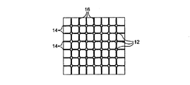
図1は、ワード線14とビット線16との交点に抵抗性メモリセル12を配置した従来のMRAMメモリアレイ10を示す。ワード線14はそのメモリアレイ10の行に沿って水平に延び、ビット線16はそのメモリアレイ10の列に沿って垂直に延びている。各メモリセル12は「1」および「0」の2値状態を格納することができる。
【0004】
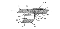
図2は従来のメモリセル12を示す。メモリセル12はスピン依存トンネル効果(「SDT」)デバイスである。メモリセル12は、ピン層(pinned layer)24と、フリー層18とを含む。ピン層24は、矢印26によって示される、固定された向きの磁化を有する。フリー層18の磁化は、双方向の矢印28によって示されており、フリー層18の「磁化容易軸」に沿って、2つの方向のいずれかに向けられることができる。フリー層18およびピン層24の磁化の向きが同じである場合には、メモリセル12の磁化の向きは「平行」である。磁化の向きが逆である場合には、その向きは「逆平行」である。2つの向きはそれぞれ、「1」および「0」の2値状態に対応する。
【0005】
フリー層18およびピン層24は、絶縁性トンネル障壁層20によって分離される。絶縁性トンネル障壁層20によって、フリー層18とピン層24との間に、量子力学的トンネル効果が生じるようになる。トンネル効果は電子スピン依存性であり、メモリセル12の抵抗は、フリー層18とピン層24との磁化の相対的な向きの関数になる。メモリセル12の抵抗は、その向きが平行である場合には「低抵抗」値Rを有し、その向きが逆平行である場合には「高抵抗」値R+ΔRを有する。
【0006】
メモリアレイ10内の各メモリセル12は、その2値状態を書込み操作によって変化させることができる。特定のメモリセル12において交差するワード線14およびビット線16に供給される書込み電流は、ピン層24に対して、フリー層18の磁化を平行と逆平行との間で切り替える。ビット線16を流れる電流Iyは、その結果として磁界Hxを生じる。電流Ixがワード線14を流れる際に同様の磁界Hyが生じる。磁界HxおよびHyを組み合わせて、メモリセル12の磁化の向きが切り替えられる。メモリセルの磁化の変化に起因する抵抗の変化を読み出し、メモリセル12の2値状態を判定することができる。
【0007】
メモリアレイ10内の各ビット線16は、スイッチ(図示せず)に接続され、各スイッチは、センス増幅器(図示せず)の入力に接続される。選択されたメモリセル12の2値状態、すなわち「ビット」は、特定のメモリセル12と交差するビット線16がセンス増幅器の入力に接続されるときに、そのメモリセル12のワード線14に読出し電圧を印加することにより読み出される。選択されたビット線16をセンス増幅器に接続するスイッチは、選択されたメモリセル12を読み出すために、交互に開閉される。
【0008】
従来のメモリアレイ10の読出し操作は、メモリアレイ10がメモリセル12の読出しの間に「整定する」ための要件によって遅くなる。選択されたビット線16をセンス増幅器に接続するスイッチが開閉される度に、ビット線16の端部の電位が変化するので、メモリアレイ10は整定しなければならない。ビット線の端部の電位の変化によって、メモリセル12の両端の電圧は、異なる平衡状態に変化する。それゆえ、読出し操作を制御するマイクロプロセッサは、読出し操作に整定時間を組み入れ、メモリセル12の読出しの間にメモリアレイ10が所望の平衡状態に整定できるようにしなければならない。単位時間当たりに読み出すことができるメモリセル12が少なくなるので、整定時間は望ましくない。
【0009】
【発明が解決しようとする課題】
したがって、メモリアレイの読出し時間を短縮することが必要とされている。
【0010】
【課題を解決するための手段】
第1の態様によれば、メモリデバイスが短縮された読出し時間を達成する。そのメモリデバイスは、メモリセルからなるメモリアレイと、交差するワード線およびビット線とを含む。センス増幅器選択スイッチのバンクが、ビット線をセンス増幅器に選択的に結合する。センス増幅器選択スイッチのバンク内の各スイッチは、センス増幅器が選択されたメモリセルの2値状態をセンシングすることができるように閉じられ得る。読出し/書込み選択スイッチのバンクは、ビット線を、列書込み電流源と、基準電圧に選択的に結合する。読出し/書込み選択スイッチのバンク内のスイッチはそれぞれ、選択されたビット線を基準電圧に結合するために閉じられ得る。読出し操作中に、センス増幅器選択スイッチのバンクおよび読出し/書込み選択スイッチのバンクは、メモリアレイ内のビット線が等電位状態にとどまるように動作する。
【0011】
第1の態様によれば、そのアレイは、ビット線とセンス増幅器との接続および切り離しによって不安定になることはない。センス増幅器は、基準電圧に設定されており、ビット線に対して読出し/書込みスイッチのバンクと同じ電位を提供する。メモリアレイ内のビット線が等電位状態から崩されることがないので、増幅器に対する切替えに起因する整定時間は必要とされない。したがって、読出し時間は従来のデバイスに比べて短くなる。
【0012】
他の態様および利点は、添付図面に関連してなされる、以下の詳細な説明から明らかになるであろう。
【0013】
【発明の実施の形態】
メモリデバイス50が、好適な実施形態を用いて、かつ図面を用いて説明される。
【0014】
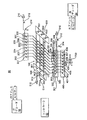
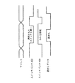
図3はメモリデバイス50の概略図である。メモリデバイス50は、コントローラ52、列デコーダ54、行デコーダ56、メモリアレイ100、書込み選択スイッチのバンク200、読出し/書込み選択スイッチのバンク300、センス増幅器選択スイッチのバンク400、読出し/書込み選択スイッチのバンク500、書込み終端選択スイッチのバンク600、およびセンス増幅器700を含む。
【0015】
コントローラ52は、行デコーダ56と列デコーダ54とを通して、メモリデバイス50の読出しおよび書込み操作を制御する。コントローラ52は、行デコーダ56に結合され、読出し/書込み(R/W)データおよびアドレスデータを含むコマンドを行デコーダ56に送信する。行デコーダ56はスイッチバンク500および600内のスイッチのゲートに結合され、コントローラ52の命令にしたがってスイッチを開閉する。同様に、コントローラ52は列デコーダ54に結合され、列デコーダ54はスイッチバンク200、300および400内のスイッチのゲートに結合される。メモリデバイス50において用いられるスイッチはトランジスタとして示される。しかしながら、たとえばFETまたはMOSFETスイッチのようなスイッチ、および他のスイッチを用いることもできる。
【0016】
メモリアレイ100は、メモリデバイス50のためのデータを格納する。メモリアレイ100において、ワード線110が水平な行内に延び、ビット線120が垂直な列内に延びている。ワード線110は、メモリセル130においてビット線120と交差する。各メモリセル130は、「1」または「0」のいずれかの2値状態を格納することができる。図3には、例示のために、24個のメモリセル130において交差する、3行のワード線110および8列のビット線120が示される。実際には、たとえば、1024×1024のメモリセル以上のアレイを用いることができる。図3には、具体例となるメモリセル130が、メモリセル130の周囲の取り巻く楕円形によって示される。このメモリセル130は、第2の行内のワード線110と、第5の列内のビット線120との交差部に存在する。
【0017】
メモリアレイ100内の任意のメモリセル130に書込みを行うために、メモリセル130が配置される列のビット線120に列書込み電流が供給され、メモリセル130が配置される行のワード線110に行書込み電流が供給される。ワード線およびビット線の書込み電流によって生じる磁界を組み合わせて、メモリセル130の2値状態を「0」から「1」に、およびその逆に変化させる。
【0018】
書込み選択スイッチのバンク200は、書込み選択スイッチ201、202、203、204、205、206、207、208を含む。各書込み選択スイッチは、メモリアレイ100のビット線120に結合される。書込み選択スイッチのバンク200によって、選択されたビット線120に列書込み電流が印加されるようになる。列書込み電流は、列書込み電流源210によって生成される。スイッチ212は、列書込み電流源210を、書込み選択スイッチのバンク200に選択的に結合する。スイッチ214は、書込み選択スイッチのバンク200をグランドに選択的に結合する。
【0019】
読出し/書込み選択スイッチのバンク300は、読出し/書込み選択スイッチ301、302、303、304、305、306、307、308を含む。各読出し/書込み選択スイッチは、メモリアレイ100のビット線120に結合される。読出し/書込み選択スイッチのバンク300によって、選択されたビット線120に列書込み電流が印加されるようになる。列書込み電流は、列書込み電流源310によって、読出し/書込み選択スイッチのバンク300に供給される。列書込み電流源310は、スイッチ312を介して、読出し/書込み選択スイッチのバンク300に選択的に結合される。読出し/書込み選択スイッチのバンク300は、スイッチ314を介して、基準電圧に選択的に結合される。図3に示される実施形態では、グランドの基準電圧が用いられる。しかしながら、他の基準電圧を用いてもよい。
【0020】
センス増幅器選択スイッチのバンク400は、センス増幅器700を、メモリアレイ100のビット線120に選択的に結合する。センス増幅器選択スイッチのバンク400は、スイッチ401、402、403、404、405、406、407、408を含み、各スイッチは対応するビット線120をセンス増幅器700に選択的に結合する。スイッチバンク400によって、センス増幅器700は、選択されたメモリセル130の2値状態を検出できるようになる。
【0021】
読出し/書込み選択スイッチのバンク500は、読出し/書込み選択スイッチ501、502、503を含む。各読出し/書込みスイッチは、メモリアレイ100のワード線110に結合される。読出し/書込み選択スイッチのバンク500は、スイッチ512を介して行書込み電流源510に結合され、スイッチ514を介して読出し電圧Vrに結合される。書込み終端選択スイッチのバンク600は、スイッチ601、602、603を含む。書込み終端選択スイッチのバンク600は、各ワード線110をグランドに選択的に結合する。行書込み電流が選択されたワード線110に供給されるとき、書込み終端選択スイッチのバンク600内の対応するスイッチが閉じられ、行書込み電流が選択されたワード線110に流れるようになる。
【0022】
ここで、図3および図4を参照して、メモリデバイス50の書込み操作を説明する。図4は、メモリデバイス50の書込み操作を示す流れ図である。
【0023】
ステップS10では、コントローラ52が、選択されたメモリセル130において交差する行および列を選択する。ステップS12では、コントローラ52が、メモリデバイス50の書込みシーケンスを開始する。ステップS14では、コントローラ52は、メモリデバイス50内の全てのスイッチを開くように設定する。
【0024】
ステップS16では、スイッチバンク500および600が、メモリアレイ100に行書込み電流を供給するためにイネーブルにされる。スイッチバンク500および600は、スイッチ512を閉じることによりイネーブルにされる。一旦、スイッチバンク500および600内の選択されたスイッチが閉じられると、スイッチ512を閉じることにより、行書込み電流が、選択されたワード線110に流れるようになる。
【0025】
ステップS18では、スイッチバンク200および300が、メモリアレイ100に列書込み電流を供給するためにイネーブルにされる。コントローラ52が、選択されたメモリセル130に「0」の状態を書き込んでいる場合には、スイッチバンク200および300が、スイッチ212、314を閉じることによりイネーブルにされる。この構成により、スイッチバンク200および300内の選択されたスイッチが閉じられた後に、列書込み電流が、列書込み電流源210から、選択されたビット線120を通り、スイッチ314を介してグランドまで流れるようになる。逆に、選択されたメモリセル130に「1」の状態が書き込まれることになる場合には、スイッチバンク200および300は、スイッチ214、312を閉じることによりイネーブルにされる。この構成により、スイッチバンク200および300内の選択されたスイッチが閉じられた後に、列書込み電流は、列書込み電流源310から、選択されたビット線120を通り、スイッチ214を介してグランドまで流れるようになる。
【0026】
ステップS20では、選択されたワード線110に行書込み電流が印加され、選択されたビット線120に列書込み電流が供給される。行書込み電流は、選択された行に対応するバンク500および600内のスイッチを閉じることにより印加される。たとえば、メモリアレイ100の第2の行および第5の列において楕円形で指示されたメモリセル130の2値状態が選択される場合には、スイッチ502および602が閉じられ、行書込み電流が、第2の行内のワード線110に流れるようになる。
【0027】
列書込み電流は、選択されたビット線120に対応するバンク200および300内のスイッチを閉じることにより印加される。上述の例では、スイッチ205および305が閉じられ、列書込み電流が、第5の列内のビット線120に流れるようになる。
【0028】
メモリアレイ100において、選択された行および列の交差部に配置されたメモリセル130は、その2値状態が書込み操作によって変更される。選択されたワード線110およびビット線120の交差部に配置される選択されたメモリセル130において結果として生じた磁界は、行および列書込み電流によって生成される磁界の和である。結果として生じた磁界は、選択されたメモリセル130の2値状態を変化させる。
【0029】
行および列書込み電流は、概ね同時に印加されるべきである。スイッチバンク内のスイッチは、行および列書込み電流が印加されている間の短い時間だけ閉じられる。たとえば、スイッチは、約1〜100ナノ秒の期間だけ閉じられ得る。
【0030】
ここで、図3、図5および図6を参照して、メモリデバイス50の読出し操作を説明する。図5は、メモリデバイス50の読出しタイミング図であり、図6はメモリデバイス50の読出し操作を示す流れ図である。
【0031】
ステップS32では、コントローラがメモリデバイスを読出しモードにする。この時点で、コントローラ52は、選択されたメモリセル130の行および列アドレスを、行デコーダ56および列デコーダ54に送信することができる。アドレスの送信は、図5の読出しタイミング図の「アドレス」タイミング線に対応する。
【0032】
ステップS34では、コントローラが読出しシーケンスを開始する。ステップS36では、メモリデバイス50内の全てのスイッチが開くように設定される。
【0033】
ステップS38では、スイッチ314および301〜308を閉じることにより、ビット線120が基準電圧に接続される。基準電圧はグランドとすることができる。図5では、例示のために、バンク300のスイッチは、「スイッチバンク300」タイミング線において、読出しタイミング図の開始時に閉じられているものとして示される。
【0034】
ステップS40では、読出し電位Vrを読出し/書込み選択スイッチのバンク500に供給するために、スイッチ514が閉じられる。
【0035】
ステップS42では、選択された行に対応するスイッチバンク500内のスイッチが閉じられ、読出し電位Vrが選択されたビット線120に印加される。たとえば、楕円形で指示されたメモリセル130が読み出されることになる場合には、スイッチ502(第2の行に対応する)が閉じられる。それにより、読出し電位Vrが、第2の行内のワード線110に印加される。メモリアレイ100が整定するまで、ある時間の経過が許可される。その整定時間によって、ビット線120内の電流が平衡状態に達することができる。図3を参照すると、これらの電流は、選択されたワード線110から、選択されたワード線110と接触するメモリセル130を通って、ビット線120、バンク300のスイッチ、スイッチ314に流れる。
【0036】
ステップS44では、選択された列に対応するスイッチバンク400内のスイッチが閉じられる。上述の例では、スイッチ405が閉じられる。残りのスイッチ401〜404および406〜408は開いたままである。スイッチバンク400内のスイッチを閉じることにより、選択された列がセンス増幅器700に接続される。この接続は、図5の読出しタイミング図の「スイッチバンク400」タイミング線において示される。
【0037】
センス増幅器700は基準電圧にある。たとえば、スイッチ314がグランドの基準電圧に接続される場合、センス増幅器700は仮想グランドにいることができる。したがって、選択されたビット線120が結合される電位は、センス増幅器700が接続される際に変化しない。読出し電流の電流経路の抵抗は、センス増幅器700が接続される際に、最低限の量だけ変化する。なぜなら、経路内の概ね全ての抵抗がメモリセル130内に存在するためである。したがって、選択されたビット線120がセンス増幅器700に接続される際に、メモリアレイ100は実質的に邪魔されない。
【0038】
ステップS46では、選択された列に対応するスイッチバンク300内のスイッチが開かれ、スイッチ314における基準電圧から選択されたビット線120を切り離す。スイッチバンク300内の残りのスイッチは閉じたままである。その例では、スイッチ305が開かれる。
【0039】
スイッチ305は開いたままであり、一方、センス増幅器700は、スイッチ405を介して選択されたビット線に接続されたままである。選択されたビット線120がセンス増幅器700に接続されたままであるので、ビット線120は基準電圧に接続されたままであり、メモリアレイ100には最小限の外乱しか存在しない。それゆえ、メモリアレイ100はその平衡した電位に維持される。
【0040】
ステップS50では、センス増幅器700が、選択されたビット線120からの電流をセンシングし、選択されたメモリセル130の2値状態を判定する。2値状態は、センス増幅器700からの出力から、コントローラ52によって検出され得る。センス増幅器700の出力は、選択されたメモリセル130の抵抗状態を示すことができる。代案として、センス増幅器700は、支援回路を含み、2値状態を判定し、その2値状態をコントローラ52に出力することができる。2値状態は、選択されたビット線120を介した電流の増減に起因して、選択されたメモリセル130の抵抗の変化として判定され得る。たとえば、高抵抗状態(逆平行状態)では結果として、メモリセル130を流れる電流は低電流になり、それは「0」の2値状態を表すことができる。低抵抗状態(平行状態)では結果として、メモリセル130を流れる電流は高電流になり、「1」の2値状態を表すことができる。
【0041】
ステップS52では、選択されたビット線120に対応するスイッチバンク300内のスイッチが閉じられる。このスイッチを閉じることにより、選択されたビット線120が、スイッチ314を介して基準電圧に結合される。ステップS54では、ビット線120に対応するスイッチバンク400内のスイッチは開かれる。このスイッチを開くことにより、選択されたビット線120がセンス増幅器700から切り離される。この時点で、メモリアレイ100内の全てのビット線120は、スイッチ314を介して、基準電圧に接続される。
【0042】
ステップS52およびS54のスイッチの開閉中に、選択されたビット線120の端部における電位は、基準電圧のままである。それゆえ、メモリアレイ100は、その平衡した電位に維持される。
【0043】
ステップS56では、コントローラ52は、選択された行内の異なるメモリセル130が読み出されることになるか否かを判定する。読み出される場合には、そのプロセスはステップS44に戻る。読み出されない場合には、ステップS58において、コントローラ52は、異なる行内のメモリセル130が読み出されることになるか否かを判定する。読み出される場合には、そのプロセスはステップS42に戻る。読み出されない場合には、読出し操作はステップS60において終了される。
【0044】
メモリアレイを読み出すことに関する上述の方法によれば、選択されたビット線120をセンス増幅器700に対して接続および切り離すことに起因する、メモリアレイ100の整定時間がなくなる。読出し操作全体を通してメモリアレイ100がその平衡した電位に維持されるので、整定時間は不要である。ビット線120が、センス増幅器700との接続および切断中に、同じ基準電圧に交互に接続されるので、平衡した電位が維持される。
【0045】
上述の実施形態では、ビット線120は、スイッチバンク300および400を介してグランドに接続される。しかしながら、これは基準電圧の単なる一例であり、他の基準電圧を用いることもできる。
【0046】
センス増幅器700は、メモリデバイス50内のメモリセル130の2値状態を検出するためのセンシング装置の一例である。実際には、たとえば、トランスインピーダンスセンス増幅器、電荷注入センス増幅器、差動センス増幅器、またはデジタル差動センス増幅器のような他のセンシング装置を用いることもできる。
【0047】
メモリセル130の2値状態をセンシングするための1つのセンス増幅器700が図3に示される。実際には、メモリアレイには、より多くの数のセンシング装置を結合することができる。たとえば、メモリアレイ内の各ビット線に対して1つのセンス増幅器を含むことができるか、またはメモリアレイ内の2つ以上のビット線毎に1つのセンス増幅器を含むことができる。
【0048】
メモリアレイに「0」および「1」の状態を書き込むために流れる電流に関する規則は、任意であり、メモリデバイス50の任意の所望の応用形態に適合するように再指定され得る。
【0049】
メモリアレイ100において用いられるメモリセル130は、読出しおよび書込み電流に応答する任意のタイプのメモリセルとすることができる。たとえば、巨大磁気抵抗(GMR)デバイス、スピントンネル接合(STJ)のようなメモリセル、および他のタイプのメモリセルをメモリデバイス50に用いることもできる。
【0050】
そのメモリデバイス50は、幅広い応用形態に用いることができる。1つの応用形態は、MRAM記憶モジュールを有するコンピューティング装置とすることができる。MRAM記憶モジュールは、長期記憶のための1つ以上のMRAMメモリアレイを含むことができる。
【0051】
MRAM記憶モジュールは、ラップトップコンピュータ、パーソナルコンピュータおよびサーバのような装置に用いることができる。
【0052】
メモリデバイス50が典型的な実施形態に関連して説明されたが、当業者には多くの変更形態が容易に明らかになるであろう。本開示はその変形形態を網羅することを意図している。
【0053】
以下においては、本発明の種々の構成要件の組み合わせからなる例示的な実施形態を示す。
1.メモリアレイ(100)を読み出す方法であって、前記メモリアレイ(100)が複数のワード線(110)と複数のビット線(120)とを含み、前記ワード線および前記ビット線が複数のメモリセル(130)において交差し、その方法が、
選択されたメモリセル(130)に結合される選択されたワード線(110)に読出し電圧(Vr)を印加するステップと、
前記選択されたメモリセルに結合される選択されたビット線(120)を、第1のスイッチ(301〜308)を介して基準電圧に結合するステップと、
前記選択されたメモリセルを、第2のスイッチ(400〜408)を介してセンシング装置(700)に結合するステップと、
前記選択されたメモリセルを前記基準電圧から切り離すために、前記第1のスイッチ(301〜308)を開くステップと、及び
前記センシング装置を用いて、前記選択されたメモリセルの2値状態を読み出すステップとからなる、方法。
2.前記第1および前記第2のスイッチが、前記選択されたビット線の端部に結合され、前記第1のスイッチを開くステップが、
前記選択されたメモリセルを前記センシング装置に結合するステップの後に、前記第1のスイッチを開くことを含む、上記1に記載の方法。
3.前記第1のスイッチを開くステップが、
前記選択されたメモリセルの2値状態を読み出すステップの前に、前記第1のスイッチを開くことを含む、上記2に記載の方法。
4.前記メモリセルの2値状態を読み出すステップの後に、前記第1のスイッチを閉じることを含む、上記3に記載の方法。
5.前記メモリセルの2値状態を読み出すステップの後に、前記第2のスイッチを開くことを含む、上記4に記載の方法。
6.選択されたワード線に読出し電圧を印加するステップが、
前記選択されたワード線に前記読出し電圧を結合するスイッチを閉じることを含む、上記5に記載の方法。
7.前記選択されたメモリセルをセンシング装置に結合するステップが、
前記選択されたビット線を前記基準電圧に結合することを含む、上記6に記載の方法。
8.前記基準電圧がグランド電位である、上記7に記載の方法。
9.前記選択されたビット線の端部の電位は、前記選択されたメモリセルが前記センシング装置に結合される際に実質的に変化しない、上記2に記載の方法。
10.前記基準電圧がグランド電位である、上記9に記載の方法。
【0054】
【発明の効果】
上記のように、本発明によれば、メモリアレイの読出し時間を短縮することが可能になる。
【図面の簡単な説明】
【図1】従来のメモリセルアレイを示す図である。
【図2】従来のメモリセルの2値状態を示す図である。
【図3】メモリデバイスの一実施形態の概略図である。
【図4】図3に示されるメモリデバイスの書込み操作を示す流れ図である。
【図5】図3に示されるメモリデバイスの読出しタイミング図である。
【図6】図3に示されるメモリデバイスの読出し動作を示す流れ図である。
【符号の説明】
50 メモリデバイス
100 メモリアレイ
110 ワード線
120 ビット線
130 メモリセル
200 書込み選択スイッチのバンク
300 読出し/書込み選択スイッチのバンク
400 センス増幅器選択スイッチのバンク
500 読出し/書込み選択スイッチのバンク
700 センス増幅器[0001]
BACKGROUND OF THE INVENTION
The technical field relates to resistive intersection memory devices. More specifically, the technical field is a memory device with reduced read time.
[0002]
[Prior art]
Magnetic random access memory ("MRAM") is one proposed type of non-volatile memory. Data access from MRAM devices is much faster than data access from conventional long-term storage devices such as hard drives. Furthermore, MRAM is more compact and consumes less power than conventional long-term storage devices.
[0003]
FIG. 1 shows a conventional MRAM memory array 10 in which
[0004]
FIG. 2 shows a
[0005]
The
[0006]
Each
[0007]
Each
[0008]
Conventional memory array 10 read operations are slowed by the requirement for memory array 10 to "settling" during
[0009]
[Problems to be solved by the invention]
Therefore, there is a need to shorten the read time of the memory array.
[0010]
[Means for Solving the Problems]
According to the first aspect, the memory device achieves a reduced read time. The memory device includes a memory array of memory cells and intersecting word lines and bit lines. A bank of sense amplifier select switches selectively couples the bit lines to the sense amplifier. Each switch in the bank of sense amplifier select switches can be closed so that the sense amplifier can sense the binary state of the selected memory cell. A bank of read / write select switches selectively couples the bit lines to a column write current source and a reference voltage. Each switch in the bank of read / write select switches can be closed to couple the selected bit line to a reference voltage. During a read operation, the sense amplifier select switch bank and the read / write select switch bank operate so that the bit lines in the memory array remain in an equipotential state.
[0011]
According to the first aspect, the array does not become unstable due to the connection and disconnection between the bit line and the sense amplifier. The sense amplifier is set to a reference voltage and provides the same potential for the bit line as the bank of read / write switches. Since the bit lines in the memory array are not destroyed from the equipotential state, no settling time due to switching to the amplifier is required. Therefore, the read time is shorter than that of the conventional device.
[0012]
Other aspects and advantages will become apparent from the following detailed description, taken in conjunction with the accompanying drawings.
[0013]
DETAILED DESCRIPTION OF THE INVENTION
The
[0014]
FIG. 3 is a schematic diagram of the
[0015]
The
[0016]
The
[0017]
In order to write to any
[0018]
The bank 200 of write selection switches includes
[0019]
The
[0020]
Sense amplifier
[0021]
The
[0022]
Here, a write operation of the
[0023]
In step S <b> 10, the
[0024]
In step S16, switch
[0025]
In step S18, switch
[0026]
In step S20, a row write current is applied to the selected
[0027]
Column write current is applied by closing the switches in
[0028]
In the
[0029]
The row and column write currents should be applied approximately simultaneously. The switches in the switch bank are closed for a short time while the row and column write currents are applied. For example, the switch can be closed for a period of about 1 to 100 nanoseconds.
[0030]
Here, the read operation of the
[0031]
In step S32, the controller sets the memory device to the read mode. At this point, the
[0032]
In step S34, the controller starts a read sequence. In step S36, all the switches in the
[0033]
In step S38, the
[0034]
In step S40, the
[0035]
In step S42, the switch in the
[0036]
In step S44, the switch in the
[0037]
The
[0038]
In step S46, the switch in the
[0039]
Switch 305 remains open, while
[0040]
In step S50, the
[0041]
In step S52, the switch in the
[0042]
During the opening and closing of the switches in steps S52 and S54, the potential at the end of the selected
[0043]
In step S56, the
[0044]
The above-described method for reading the memory array eliminates the settling time of the
[0045]
In the above-described embodiment, the
[0046]
The
[0047]
One
[0048]
The rules for the currents flowing to write the “0” and “1” states to the memory array are arbitrary and can be respecified to suit any desired application of the
[0049]
The
[0050]
The
[0051]
The MRAM storage module can be used in devices such as laptop computers, personal computers and servers.
[0052]
Although the
[0053]
In the following, exemplary embodiments consisting of combinations of various components of the present invention are shown.
1. A method of reading a memory array (100), wherein the memory array (100) includes a plurality of word lines (110) and a plurality of bit lines (120), and the word lines and the bit lines are a plurality of memory cells. At (130), the method
Applying a read voltage (Vr) to a selected word line (110) coupled to a selected memory cell (130);
Coupling a selected bit line (120) coupled to the selected memory cell to a reference voltage via a first switch (301-308);
Coupling the selected memory cell to a sensing device (700) via a second switch (400-408);
Opening the first switch (301-308) to decouple the selected memory cell from the reference voltage; and
Reading the binary state of the selected memory cell using the sensing device.
2. The first and second switches being coupled to an end of the selected bit line and opening the first switch;
The method of claim 1, comprising opening the first switch after coupling the selected memory cell to the sensing device.
3. Opening the first switch comprises:
3. The method of claim 2, comprising opening the first switch before reading the binary state of the selected memory cell.
4). 4. The method of claim 3, comprising closing the first switch after reading the binary state of the memory cell.
5. 5. The method of claim 4, comprising opening the second switch after reading the binary state of the memory cell.
6). Applying a read voltage to the selected word line comprises:
6. The method of claim 5, comprising closing a switch that couples the read voltage to the selected word line.
7). Coupling the selected memory cell to a sensing device;
The method of claim 6, comprising coupling the selected bit line to the reference voltage.
8). 8. The method according to 7 above, wherein the reference voltage is a ground potential.
9. The method of claim 2, wherein the potential at the end of the selected bit line does not substantially change when the selected memory cell is coupled to the sensing device.
10. 10. The method according to 9 above, wherein the reference voltage is a ground potential.
[0054]
【The invention's effect】
As described above, according to the present invention, it is possible to shorten the read time of the memory array.
[Brief description of the drawings]
FIG. 1 shows a conventional memory cell array.
FIG. 2 is a diagram showing a binary state of a conventional memory cell.
FIG. 3 is a schematic diagram of one embodiment of a memory device.
4 is a flowchart illustrating a write operation of the memory device shown in FIG.
FIG. 5 is a read timing diagram of the memory device shown in FIG. 3;
6 is a flowchart showing a read operation of the memory device shown in FIG. 3;
[Explanation of symbols]
50 memory devices
100 memory array
110 word lines
120 bit line
130 memory cells
Bank of 200 write selection switches
300 Bank of read / write selection switches
Bank of 400 sense amplifier selection switches
Bank of 500 read / write select switches
700 sense amplifier
Claims (5)
選択されたメモリセルに結合される選択されたビット線(120)を、第1のスイッチ(301〜308)を介してグランド電位に結合する第1ステップと、
前記第1ステップの後、選択されたメモリセル(130)に結合される選択されたワード線(110)に読出し電圧(Vr)を印加する第2ステップと、
前記第2ステップの後、前記選択されたメモリセルに結合される選択されたビット線(120)を、第2のスイッチ(400〜408)を介してセンシング装置(700)に結合する第3ステップと、
前記第3ステップの後、前記選択されたメモリセルに結合される選択されたビット線(120)を前記グランド電位から切り離すために、前記第1のスイッチ(301〜308)を開く第4ステップと、
前記第4ステップの後、前記センシング装置を用いて、前記選択されたメモリセルの2値状態を読み出す第5ステップとからなり、
前記第1及び前記第2のスイッチが、前記選択されたビット線の端部に結合される、方法。A method of reading a memory array (100), wherein the memory array (100) is arranged at a plurality of word lines (110), a plurality of bit lines (120), and intersections of the word lines and the bit lines, respectively. A plurality of memory cells (130), the method comprising:
A first step of coupling a selected bit line (120) coupled to a selected memory cell to a ground potential via a first switch (301-308);
A second step of applying a read voltage (Vr) to the selected word line (110) coupled to the selected memory cell (130) after the first step ;
After the second step, a third step of coupling said selected selected bit line coupled to the memory cell (120), in through the second switch (400-408) sensing apparatus (700) When,
After the third step, a fourth step of opening the first switch (301-308) to disconnect the selected bit line (120) coupled to the selected memory cell from the ground potential ; ,
After the fourth step, using the sensing device, the fifth step of reading the binary state of the selected memory cell,
The method wherein the first and second switches are coupled to an end of the selected bit line.
Applications Claiming Priority (2)
| Application Number | Priority Date | Filing Date | Title |
|---|---|---|---|
| US09/910,823 US6515896B1 (en) | 2001-07-24 | 2001-07-24 | Memory device with short read time |
| US09/910823 | 2001-07-24 |
Publications (3)
| Publication Number | Publication Date |
|---|---|
| JP2003059258A JP2003059258A (en) | 2003-02-28 |
| JP2003059258A5 JP2003059258A5 (en) | 2005-05-12 |
| JP4067897B2 true JP4067897B2 (en) | 2008-03-26 |
Family
ID=25429375
Family Applications (1)
| Application Number | Title | Priority Date | Filing Date |
|---|---|---|---|
| JP2002207874A Expired - Fee Related JP4067897B2 (en) | 2001-07-24 | 2002-07-17 | Memory device with reduced read time |
Country Status (6)
| Country | Link |
|---|---|
| US (1) | US6515896B1 (en) |
| EP (1) | EP1288959A3 (en) |
| JP (1) | JP4067897B2 (en) |
| KR (1) | KR100845524B1 (en) |
| CN (1) | CN1229807C (en) |
| TW (1) | TWI222062B (en) |
Families Citing this family (9)
| Publication number | Priority date | Publication date | Assignee | Title |
|---|---|---|---|---|
| JP2002170377A (en) * | 2000-09-22 | 2002-06-14 | Mitsubishi Electric Corp | Thin film magnetic storage device |
| US6724651B2 (en) * | 2001-04-06 | 2004-04-20 | Canon Kabushiki Kaisha | Nonvolatile solid-state memory and method of driving the same |
| DE10123593C2 (en) * | 2001-05-15 | 2003-03-27 | Infineon Technologies Ag | Magnetic storage device |
| US6778431B2 (en) * | 2002-12-13 | 2004-08-17 | International Business Machines Corporation | Architecture for high-speed magnetic memories |
| US6775195B1 (en) | 2003-02-28 | 2004-08-10 | Union Semiconductor Technology Center | Apparatus and method for accessing a magnetoresistive random access memory array |
| US7454586B2 (en) * | 2005-03-30 | 2008-11-18 | Intel Corporation | Memory device commands |
| US20060236027A1 (en) * | 2005-03-30 | 2006-10-19 | Sandeep Jain | Variable memory array self-refresh rates in suspend and standby modes |
| JP4883982B2 (en) * | 2005-10-19 | 2012-02-22 | ルネサスエレクトロニクス株式会社 | Nonvolatile memory device |
| CN105006244B (en) * | 2015-05-13 | 2017-10-10 | 湖北中部慧易数据科技有限公司 | A kind of signal amplifier, the reading circuit of magnetic memory and its operating method |
Family Cites Families (25)
| Publication number | Priority date | Publication date | Assignee | Title |
|---|---|---|---|---|
| US4061999A (en) * | 1975-12-29 | 1977-12-06 | Mostek Corporation | Dynamic random access memory system |
| US5784327A (en) * | 1991-06-12 | 1998-07-21 | Hazani; Emanuel | Memory cell array selection circuits |
| US5477482A (en) | 1993-10-01 | 1995-12-19 | The United States Of America As Represented By The Secretary Of The Navy | Ultra high density, non-volatile ferromagnetic random access memory |
| US5640343A (en) | 1996-03-18 | 1997-06-17 | International Business Machines Corporation | Magnetic memory array using magnetic tunnel junction devices in the memory cells |
| JP2848325B2 (en) * | 1996-03-28 | 1999-01-20 | 日本電気株式会社 | Semiconductor storage device |
| US5748519A (en) | 1996-12-13 | 1998-05-05 | Motorola, Inc. | Method of selecting a memory cell in a magnetic random access memory device |
| JPH10223991A (en) | 1997-01-31 | 1998-08-21 | Ando Electric Co Ltd | Variable wavelength laser light source |
| US5852574A (en) | 1997-12-24 | 1998-12-22 | Motorola, Inc. | High density magnetoresistive random access memory device and operating method thereof |
| US6219273B1 (en) * | 1998-03-02 | 2001-04-17 | California Institute Of Technology | Integrated semiconductor-magnetic random access memory system |
| US5986925A (en) | 1998-04-07 | 1999-11-16 | Motorola, Inc. | Magnetoresistive random access memory device providing simultaneous reading of two cells and operating method |
| US5946227A (en) * | 1998-07-20 | 1999-08-31 | Motorola, Inc. | Magnetoresistive random access memory with shared word and digit lines |
| US6111781A (en) * | 1998-08-03 | 2000-08-29 | Motorola, Inc. | Magnetic random access memory array divided into a plurality of memory banks |
| US5969978A (en) | 1998-09-30 | 1999-10-19 | The United States Of America As Represented By The Secretary Of The Navy | Read/write memory architecture employing closed ring elements |
| DE19853447A1 (en) * | 1998-11-19 | 2000-05-25 | Siemens Ag | Magnetic storage |
| US6055178A (en) | 1998-12-18 | 2000-04-25 | Motorola, Inc. | Magnetic random access memory with a reference memory array |
| DE50000262D1 (en) * | 1999-01-13 | 2002-08-08 | Infineon Technologies Ag | WRITING / READING ARCHITECTURE FOR MRAM |
| US6134138A (en) | 1999-07-30 | 2000-10-17 | Honeywell Inc. | Method and apparatus for reading a magnetoresistive memory |
| US6609174B1 (en) * | 1999-10-19 | 2003-08-19 | Motorola, Inc. | Embedded MRAMs including dual read ports |
| US6128239A (en) | 1999-10-29 | 2000-10-03 | Hewlett-Packard | MRAM device including analog sense amplifiers |
| US6188615B1 (en) | 1999-10-29 | 2001-02-13 | Hewlett-Packard Company | MRAM device including digital sense amplifiers |
| US6473336B2 (en) * | 1999-12-16 | 2002-10-29 | Kabushiki Kaisha Toshiba | Magnetic memory device |
| US6185143B1 (en) | 2000-02-04 | 2001-02-06 | Hewlett-Packard Company | Magnetic random access memory (MRAM) device including differential sense amplifiers |
| KR100451096B1 (en) * | 2000-09-19 | 2004-10-02 | 엔이씨 일렉트로닉스 가부시키가이샤 | Non-volatile semiconductor memory device with magnetic memory cell array |
| JP4667594B2 (en) * | 2000-12-25 | 2011-04-13 | ルネサスエレクトロニクス株式会社 | Thin film magnetic memory device |
| JP3812805B2 (en) * | 2001-01-16 | 2006-08-23 | 日本電気株式会社 | Semiconductor memory device using tunnel magnetoresistive element |
-
2001
- 2001-07-24 US US09/910,823 patent/US6515896B1/en not_active Expired - Lifetime
-
2002
- 2002-06-10 TW TW091112535A patent/TWI222062B/en not_active IP Right Cessation
- 2002-07-17 JP JP2002207874A patent/JP4067897B2/en not_active Expired - Fee Related
- 2002-07-19 EP EP02255074A patent/EP1288959A3/en not_active Withdrawn
- 2002-07-23 KR KR1020020043145A patent/KR100845524B1/en active IP Right Grant
- 2002-07-24 CN CNB021269521A patent/CN1229807C/en not_active Expired - Lifetime
Also Published As
| Publication number | Publication date |
|---|---|
| JP2003059258A (en) | 2003-02-28 |
| EP1288959A2 (en) | 2003-03-05 |
| US20030021145A1 (en) | 2003-01-30 |
| CN1229807C (en) | 2005-11-30 |
| KR20030011595A (en) | 2003-02-11 |
| US6515896B1 (en) | 2003-02-04 |
| CN1399276A (en) | 2003-02-26 |
| TWI222062B (en) | 2004-10-11 |
| KR100845524B1 (en) | 2008-07-10 |
| EP1288959A3 (en) | 2003-12-10 |
Similar Documents
| Publication | Publication Date | Title |
|---|---|---|
| US6385111B2 (en) | Reference signal generation for magnetic random access memory devices | |
| JP4758554B2 (en) | MRAM device | |
| US6317375B1 (en) | Method and apparatus for reading memory cells of a resistive cross point array | |
| US6807088B2 (en) | Magnetic random access memory and reading method thereof | |
| JP4071531B2 (en) | Thin film magnetic memory device | |
| US20020027803A1 (en) | Magnetic memory device and method of reading data in magnetic memory device | |
| US6906941B2 (en) | Magnetic memory structure | |
| KR101123925B1 (en) | System and method for reading a memory cell | |
| JP4532909B2 (en) | Multistage cell magnetoresistive random access memory | |
| JP2004280892A (en) | Semiconductor storage device and its control method | |
| US6822895B2 (en) | Magnetic memory device | |
| US7440314B2 (en) | Toggle-type magnetoresistive random access memory | |
| JP4067897B2 (en) | Memory device with reduced read time | |
| KR101054363B1 (en) | Method and system for performing read operations | |
| US7751231B2 (en) | Method and integrated circuit for determining the state of a resistivity changing memory cell | |
| US7203088B2 (en) | Magnetoresistive random access memory and driving method thereof | |
| US6925003B2 (en) | Magnetic memory cell structure | |
| JP2004006861A (en) | Magnetic random access memory whose parasitic current is reduced |
Legal Events
| Date | Code | Title | Description |
|---|---|---|---|
| A521 | Request for written amendment filed |
Free format text: JAPANESE INTERMEDIATE CODE: A523 Effective date: 20040630 |
|
| A621 | Written request for application examination |
Free format text: JAPANESE INTERMEDIATE CODE: A621 Effective date: 20040630 |
|
| A977 | Report on retrieval |
Free format text: JAPANESE INTERMEDIATE CODE: A971007 Effective date: 20061121 |
|
| A131 | Notification of reasons for refusal |
Free format text: JAPANESE INTERMEDIATE CODE: A131 Effective date: 20061128 |
|
| A601 | Written request for extension of time |
Free format text: JAPANESE INTERMEDIATE CODE: A601 Effective date: 20070228 |
|
| A602 | Written permission of extension of time |
Free format text: JAPANESE INTERMEDIATE CODE: A602 Effective date: 20070305 |
|
| A521 | Request for written amendment filed |
Free format text: JAPANESE INTERMEDIATE CODE: A523 Effective date: 20070510 |
|
| A02 | Decision of refusal |
Free format text: JAPANESE INTERMEDIATE CODE: A02 Effective date: 20070619 |
|
| A711 | Notification of change in applicant |
Free format text: JAPANESE INTERMEDIATE CODE: A711 Effective date: 20070821 |
|
| A521 | Request for written amendment filed |
Free format text: JAPANESE INTERMEDIATE CODE: A523 Effective date: 20070918 |
|
| A911 | Transfer to examiner for re-examination before appeal (zenchi) |
Free format text: JAPANESE INTERMEDIATE CODE: A911 Effective date: 20071113 |
|
| TRDD | Decision of grant or rejection written | ||
| A01 | Written decision to grant a patent or to grant a registration (utility model) |
Free format text: JAPANESE INTERMEDIATE CODE: A01 Effective date: 20071218 |
|
| A61 | First payment of annual fees (during grant procedure) |
Free format text: JAPANESE INTERMEDIATE CODE: A61 Effective date: 20080109 |
|
| FPAY | Renewal fee payment (event date is renewal date of database) |
Free format text: PAYMENT UNTIL: 20110118 Year of fee payment: 3 |
|
| R150 | Certificate of patent or registration of utility model |
Free format text: JAPANESE INTERMEDIATE CODE: R150 Ref document number: 4067897 Country of ref document: JP Free format text: JAPANESE INTERMEDIATE CODE: R150 |
|
| FPAY | Renewal fee payment (event date is renewal date of database) |
Free format text: PAYMENT UNTIL: 20120118 Year of fee payment: 4 |
|
| R250 | Receipt of annual fees |
Free format text: JAPANESE INTERMEDIATE CODE: R250 |
|
| FPAY | Renewal fee payment (event date is renewal date of database) |
Free format text: PAYMENT UNTIL: 20130118 Year of fee payment: 5 |
|
| R250 | Receipt of annual fees |
Free format text: JAPANESE INTERMEDIATE CODE: R250 |
|
| FPAY | Renewal fee payment (event date is renewal date of database) |
Free format text: PAYMENT UNTIL: 20140118 Year of fee payment: 6 |
|
| R250 | Receipt of annual fees |
Free format text: JAPANESE INTERMEDIATE CODE: R250 |
|
| R250 | Receipt of annual fees |
Free format text: JAPANESE INTERMEDIATE CODE: R250 |
|
| R250 | Receipt of annual fees |
Free format text: JAPANESE INTERMEDIATE CODE: R250 |
|
| R250 | Receipt of annual fees |
Free format text: JAPANESE INTERMEDIATE CODE: R250 |
|
| R250 | Receipt of annual fees |
Free format text: JAPANESE INTERMEDIATE CODE: R250 |
|
| R250 | Receipt of annual fees |
Free format text: JAPANESE INTERMEDIATE CODE: R250 |
|
| R250 | Receipt of annual fees |
Free format text: JAPANESE INTERMEDIATE CODE: R250 |
|
| R250 | Receipt of annual fees |
Free format text: JAPANESE INTERMEDIATE CODE: R250 |
|
| R250 | Receipt of annual fees |
Free format text: JAPANESE INTERMEDIATE CODE: R250 |
|
| LAPS | Cancellation because of no payment of annual fees |