JP4065481B2 - Developing device and cartridge - Google Patents
Developing device and cartridge Download PDFInfo
- Publication number
- JP4065481B2 JP4065481B2 JP2001224603A JP2001224603A JP4065481B2 JP 4065481 B2 JP4065481 B2 JP 4065481B2 JP 2001224603 A JP2001224603 A JP 2001224603A JP 2001224603 A JP2001224603 A JP 2001224603A JP 4065481 B2 JP4065481 B2 JP 4065481B2
- Authority
- JP
- Japan
- Prior art keywords
- developer
- magnetic
- developing
- carrier
- magnetic field
- Prior art date
- Legal status (The legal status is an assumption and is not a legal conclusion. Google has not performed a legal analysis and makes no representation as to the accuracy of the status listed.)
- Expired - Fee Related
Links
Images


Description
【0001】
【発明の属する技術分野】
本発明は、像担持体上に形成された静電潜像を現像する現像装置、又は前記現像装置を有し画像形成装置に着脱可能なカートリッジに関し、特に、複写機、プリンタ、FAX等の画像形成装置において用いられる現像装置、又はカートリッジに関する。
【0002】
【従来の技術】
従来、電子写真方式を用いた画像形成装置に用いられる現像装置としては各種装置が提案されまた実用化されている。大別すると、一成分現像方式による現像装置と二成分現像方式による現像装置とに分けられる。一成分現像方式に於いてはほとんどが非接触方式であり、代表的な現像法としては磁性トナーを用いた一成分ジャンピング現像方法がある。
【0003】
この現像方法は、容易な構成で高品位な画質を得られるが、トナーに磁性体が含まれるため、カラー画像を得ることができないという欠点がある。また、非磁性トナーを用いた一成分現像方法は、カラー画像を得ることができるが、現像スリーブ上にトナーを塗布することが困難で、弾性ブレードによってコーティングしているのが現状であり、安定性や耐久性に欠ける面がある。
【0004】
一方、二成分現像法は、磁性キャリアによりトナーを現像領域に搬送し現像を行うものであり、通常は、現像剤を感光ドラムに接触させて現像工程を行う。ここでその現像工程について図6を用いて説明する。
【0005】
図中、30は現像スリーブ、35は現像スリーブ内に固定配置されたマグネットローラー、31、32は撹拌スクリュー、33は現像剤を現像スリーブ表面に薄層形成するために配置された規制ブレード、34は現像容器である。ここで前記静電潜像を、上記現像装置を用いて二成分磁気ブラシ法により顕像化する現像工程と現像剤の循環系について以下に説明する。まず、現像スリーブ30の回転に伴い、N3極で汲み上げられた現像剤は、S2極→N1極と搬送される過程において、規制ブレード33によって規制され、現像スリーブ30上に薄層形成される。
【0006】
ここで薄層形成された現像剤が、現像主極S1極に搬送されてくると磁気力により穂立ちが形成される。この穂状に形成された現像剤によって前記静電潜像を現像し、その後N2極、N3極の反発磁界によって現像スリーブ30上の現像剤は現像容器内34内に戻される。二成分現像に於いては、上述したように、同極性の磁極を並べて配置し、現像後の現像剤を一旦現像スリーブから剥ぎ取り、画像履歴を残さないようにする構成が一般的である。
【0007】
現像スリーブには図示しない電源から直流バイアス及び交流バイアスが印加されている。一般に二成分現像方法に於いては、交流バイアスを印加することで現像効率が増し、画像が高品位になる。
【0008】
潜像形成方法としては、被記録画像信号に対応して変調されたレーザービームにより電子写真感光体を走査露光し、ドット分布形状即ちドット状の潜像を画像に対応して分布させた静電潜像を形成する方法が知られている。その中でもレーザーの駆動パルス電流の幅(即ち継続時間)を被記録画像の濃淡に対応して変調する、所謂パルス幅変調(PWM)法は、高記録密度(即ち高解像度)を得ることができ、かつ高い階調性を得ることができるものである。
【0009】
ところで、近年、二成分現像器を用いた、更なる、高画質化、長寿命化の開発が進められている。その中で、長寿命化を達成するためには、現像剤が圧縮されない構成を取り、トナー及びキャリアの劣化を防止することが必要である。そのための方法の一つとしては、現像剤中の磁性キャリアの磁化を小さくする方法がある。キャリアの磁化を小さくする方向は、現像部に於いて、感光体上に現像されたトナー像を摺擦する力が弱くなるという点で高画質化の方向でもある。
【0010】
キャリアの磁化を小さくし、現像スリーブと感光ドラムが順方向回転する場合、上記のような利点はあるものの、欠点も生じる。現像部において、磁気ブラシの長さが短くなり、現像剤が感光ドラムに接触しているNIP(周方向)が狭くなることより、黒ベタ後端の濃度が濃くなる、所謂はきよせ等のエッジ強調が目立つようになる。
【0011】
この現象は、現像スリーブと感光ドラムの回転方向がその対向部で順方向回転する場合、黒ベタ現像時、上述した現像剤が感光ドラムに接触しているNIPの上流側で、感光ドラム側にトナーが滞留し、ソリッド部では現像不良のため感光ドラム上にトナーがあまり付着せず、(黒ベタの)後端に滞留トナーが一気に付着し発生する。
【0012】
磁気ブラシ長が長い場合には、磁気ブラシが接触しているNIPが長くなり、滞留トナーが発生せず、黒ベタ後端のはきよせは発生しない。また、現像スリーブと感光ドラムをその対向部で互いに逆回転するカウンター現像では、上述したNIP上流側の、感光ドラム側での滞留がなくなることで、キャリアの磁化を小さくし、磁気ブラシ長を短くしても、はきよせ等のエッジ強調は発生しづらくなる。
【0013】
順方向で発生する滞留現象は、磁気ブラシが接触しているNIPの、感光ドラムの回転方向上流側(現像スリーブ回転方向上流側)の感光ドラム上で発生する。ところが、カウンター現像では、現像スリーブと感光ドラムが互いに逆方向に移動することより、実際にはこのトナーは、滞留せずに、感光ドラムの回転によりNIP域外に運ばれて、はきよせ等の原因となる滞留はしない。
【0014】
一方、現像装置を製造、組み立てする際に、現像容器内に導電性磁性粉が混入してしまうことがあった。例えば、現像スリーブが取り付けられた状態の現像容器に蓋をして現像装置として完成させる場合、ビスを用いて蓋を現像容器に固定するとき、ビスとビットインサートとの間でのビスの削れ粉、即ち、導電性磁性粉が現像容器内に入り込んでしまう場合があった。また、現像容器を組み立てする作業者の衣服あるいは作業工具(例えば、ドライバー等)に導電性磁性粉が付着していることがあり、これが現像容器の組み立ての際に入り込んでしまうことがあった。このように、現像装置(現像容器)の製造、組み立て過程や、現像装置(現像容器)の交換過程において、導電性磁性粉が入り込んでしまうことがあった。
【0015】
また、静電潜像を形成するために感光体を帯電するのにコロナ帯電方式を採用した一次帯電器を用いる場合、一次帯電器の放電ワイヤーをリフレッシュ(使用するに連れて付着してしまう放電生成物を取り除いて放電効率を向上させるため)するべく、ユーザーやサービスマンにより放電ワイヤーを手動で削るあるいは自動的に削る際に発生した導電性磁性粉が現像容器内に何らかの原因で混入してしまうこともあった。
【0016】
しかしながら、上記のような構成、すなわちキャリアの磁化の大きさを小さくし、現像スリーブと感光ドラムがその対向部で互いにカウンター方向に回転するような構成で現像を行う場合、現像容器内に導電性磁性粉が混入してしまった時に、放電跡(マーク)が連続して線状に発生した。そして、この線状に発生した放電跡の最大長さは、700mmにまで達することもあった。
【0017】
この放電現象は、放電跡が連なって発生することが少なく、1個1個独立に発生することがあった。1個1個の放電跡は、真ん中が白く抜け、その周りがリング状に濃くでたり、全面濃くでたり、様々である。そして、ベタ白部にも、ベタ黒部にも発生する。放電跡が連続して線状に発生すると、その放電跡は、目立ち、大いに画像品位が低下してしまう。
【0018】
【発明が解決しようとする課題】
本発明の目的は、現像容器内に導電性磁性粉が入ってしまうことがあっても、放電跡の発生率を少なくすることができる現像装置を提供することである。
【0019】
本発明の他の目的は、仮に放電跡が線状に発生した場合であってもその最大長さを短くすることができる現像装置を提供することである。
【0020】
本発明の他の目的は、現像容器内に導電性磁性粉が入ってしまうことがあっても、放電跡の発生率を少なくすることができるカートリッジを提供することである。
【0021】
本発明の他の目的は、仮に放電跡が線状に発生した場合であってもその最大長さを短くすることができるカートリッジを提供することである。
【0022】
【課題を解決するための手段】
本発明は、非磁性トナーと磁性キャリアを備える現像剤を収容する現像容器と、前記現像容器内の現像剤を担持して搬送する現像剤担持体と、該現像剤担持体に現像バイアスを印加する電源と、現像剤担持体内に設けられ磁界を発生する磁界発生手段とを有し、像担持体上に形成された静電潜像を、磁界発生手段により現像剤担持体上に形成された磁気ブラシにより現像し、磁性キャリアの磁化は、0.1テスラの磁界において3.0×10 4 〜2.0×10 5 A/mであり、像担持体と現像剤担持体との最近接部において像担持体及び現像剤担持体の移動方向は互いに逆方向であり、現像剤担持体表面の接線方向における磁界発生手段による磁場の強さをBθ、現像剤担持体表面に垂直な方向における磁界発生手段による磁場の強さをBrとすると、現像剤担持体表面に垂直な方向における磁界発生手段による磁気力Frは、Fr=A・∇r{(Br) 2 +(Bθ) 2 }(Aは定数)と表され、Frのピーク位置は、最近接部と、最近接部から現像剤担持体の回転方向下流側に15°離れた位置との間に位置する現像装置を提供する。
【0023】
【発明の実施の形態】
以下の実施例では、静電潜像の現像において、磁界発生手段によって現像剤に作用する磁気力(磁気吸引力)のピーク位置を規定することにより、現像容器内に導電性磁性粉が入ってしまうことがあっても放電跡の発生率を少なくし、放電跡が線状に発生した場合にもその最大長さを短くしようとするものである。画像形成方法としては、後述するような現像剤の供給工程を行い、像担持体に形成された静電潜像を二成分現像剤により現像して用紙等に記録する方法であれば特に限定されず、従来より知られている電子写真方式や静電記録方式等の画像形成方法を採用することができる。
【0024】
画像形成装置は、後述する磁界発生手段による磁界の強さ等の特徴を少なくとも有していれば、従来より知られている種々の構成を用いることができる。このような構成としては、像担持体としての感光体(例えば、有機感光体)、像担持体を帯電する帯電装置(コロナ帯電器)、帯電された像担持体に形成すべき画像(例えば、複写原稿の画像)に対応する静電潜像を形成する露光装置、像担持体と現像剤担持体との間の最近接部(現像部)において像担持体上に形成された静電潜像を磁界発生手段により現像剤担持体上に形成された磁気ブラシ(現像剤担持体上に磁界により穂立ちされたキャリアがブラシ状に形成される。キャリアはトナーを担持しており、このトナーが像担持体上の静電潜像に付着することにより現像が行われる。)を前記像担持体に接触させて現像する現像装置、現像により得られたトナー像を普通紙等の転写材に転写する転写装置、転写された未定着トナー像を加熱加圧して定着する定着装置、転写後の像担持体に残留するトナーを除去するクリーニング装置等を例示することができる。
【0025】
現像装置は、現像剤担持体としての回転可能な非磁性円筒(現像スリーブ)と、非磁性円筒内部に固定配置される磁界発生手段としてのマグネットローラと、二成分現像剤を収容する現像容器と、を少なくとも有する。なお、本発明では、現像時、最近接部(現像部)において、非磁性円筒と静電潜像を担持する像担持体との移動方向は互いに逆方向、すなわち対向方向(カウンター方向)である。
【0026】
前記非磁性円筒は、導電性の材料によって形成されることが好ましく、このような材料としては、例えばステンレスやアルミニウム等の金属、導電性粒子の分散により導電性を付与した樹脂体等、従来より知られている種々の材料を例示することができる。また、非磁性円筒には、二成分現像剤の搬送性を高めるために、ブラスト処理等により表面を粗面化するなどの加工を施しても良い。
【0027】
磁界発生手段(マグネットローラ)は、非磁性円筒に対して相対的に不動となるように、複数の磁極(N極やS極)が非磁性円筒の内部に固定される。磁界発生手段には、常時磁界を発生する磁石等の手段であっても良いし、一定の磁界、又は異なる極性の磁界を任意に発生させることのできる電磁石等の手段であっても良い。
【0028】
なお、本実施例では、現像後、現像スリーブ上から現像剤を剥ぎ取るための同極性の反発磁極(S1、S3)を備えており、この反発磁極のうち現像スリーブ回転方向下流側のS3と略対向するように、現像スリーブ上に汲み上げられた現像剤の層厚を規制する規制部材(規制ブレード)が配置されている。また、現像スリーブは、現像剤を重力方向下方側から上方へ向けて現像部に搬送する構成となっている。このような構成とすることにより、現像スリーブ上に汲み上げられた現像剤に対し過大に圧縮する(過大な負荷をかける)のを防止することができるので、長期に亘って現像剤(特にキャリア)の特性が変動してしまうのを防止できる。
【0029】
本実施例では、非磁性円筒表面の任意の位置における磁界発生手段による磁気力F(ベクトル)のうち非磁性円筒表面に垂直な方向(法線方向)の成分である磁気力Frのピーク位置は、最近接部(現像部)近傍であって、最近接部よりも非磁性円筒の回転方向下流側に位置している。即ち、非磁性円筒表面の任意の位置における磁界発生手段による磁界の強さ(磁束密度ともいう)B(ベクトル)のうち接線方向成分をBθとすると、Brの絶対値の自乗とBθの絶対値の自乗との和の、非磁性円筒面に垂直な方向に対する傾きのピーク位置は、最近接部(現像部)近傍であって、最近接部よりも非磁性円筒の回転方向下流側に位置している。
【0030】
さらに、前記Brのピーク位置も、最近接部(現像部)近傍であって、最近接部よりも非磁性円筒の回転方向下流側に位置している。
以下、この理由について説明する。
【0031】
前記Brの絶対値の自乗と前記Bθの絶対値の自乗との和の、非磁性円筒面に垂直な方向に対する傾きとは、非磁性円筒内に固定されている磁界発生手段により、非磁性円筒にトナーを担持した磁性キャリアを引き付ける力(磁気吸引力)を表している。
【0032】
磁性キャリア1個に対して、非磁性円筒面に垂直に働く磁気力Fr(単位;Nニュートン)は、磁性キャリアの磁化をm(ベクトル、|m|の単位はA/m)、磁性キャリア1個の体積をV(m3)、マグネットローラによる磁界の強さをB(B=(Br,Bθ))、非磁性円筒(現像スリーブ)の回転中心に向かう方向を正(プラス)方向とすると、
Fr=−A∇r(m・B)
=−Ad/dr(|m|VB・B)
=−|m|VAd/dr(B2)
=−|m|VAd/dr{(Br)2+(Bθ)2}
と表される。ここで、Aは定数、|m|は透磁率の関数であり、rをスリーブ面に対して放射方向(法線方向)に設定したので、力の方向は、スリーブの中心に向かう方向の力である。
【0033】
したがって、スリーブ面上で、スリーブ面に垂直に働く力Frは、Brの絶対値の自乗とBθの絶対値の自乗の和の、現像スリーブ面に垂直な方向に対する傾き(スリーブの中心に向かう方向を正(プラス)とする。)に比例する。
【0034】
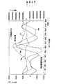
上記Br、Bθ、Fr、Fθの現像スリーブ周方向における強度分布の一例として図5に示す。左側の縦軸は、ガウス(G)、右側の縦軸は強度を表し、単位は無次元(a.u.)となっている。横軸は、現像スリーブの周方向における位置、即ち、角度を表しており(現像スリーブの回転方向は、図5上、左側から右側に向かう方向となっている)「Sl/Dr対向部」は現像スリーブと感光体との最近接部を意味している。図5から分かるように、Frのピーク位置は最近接部(Sl/Dr対向部)よりも僅かに下流側に位置しており、この位置でFθはプラス側からマイナス側に移行している。Fθがプラス側では、Frのピークに向かわせる力を現像剤に対して作用していることを意味している。
【0035】
以上のように、前記Brの絶対値の自乗と前記Bθの絶対値の自乗との和の、非磁性円筒面に垂直な方向に対する傾きのピーク位置が現像部(最近接部)近傍であって、現像部よりも非磁性円筒の回転方向下流側に位置することにより、前述したような導電性磁性粉が混入してしまうことが発生しても、現像部に向けて非磁性円筒により搬送されてきた導電性磁性粉が現像部よりも非磁性円筒の回転方向下流側に位置するFrのピーク位置に引き付けられることになる。
【0036】
また、図5から、現像部の上流側では、Fθ(キャリア(磁性体)に対してスリーブ表面の接線方向に作用する力)によって現像剤はFrのピーク位置に向かわせる力を受けていることを表している。即ち、導電性磁性粉が上流側において滞留しないように構成されていることが分かる。
【0037】
したがって、非磁性円筒上の導電性磁性粉は現像部よりも非磁性円筒の回転方向上流側(現像部入口側)で滞留することなく現像部(最近接部)を通過し、上記したような放電跡が発生するのを防止することができる。また、万が一、放電跡が発生するようなことがあっても、その放電跡の連続発生、放電跡の発生頻度、放電跡の出現規模を抑制することが可能となる。
【0038】
なお、上記Frのピーク位置を、最近接部(現像部)と、最近接部よりも非磁性円筒の回転方向下流側に15°の位置との間に位置するように設定するのが好ましい。
【0039】
上記Frピーク位置が非磁性円筒の回転方向下流側に15°の位置よりもさらに下流側に離れてしまうと、前記導電性磁性粉に対する力の作用が小さくなり、上記導電性磁性粉の滞留防止効果が不十分となることがあった。なお、以下で説明する実施例では、現像スリーブの直径が16mmであるので、最近接部と、最近接部よりも非磁性円筒の回転方向下流側に15°の位置との間の現像スリーブ周方向の距離は約2.1mmとなる。
【0040】
本実施例において最近接部とは、非磁性円筒の表面と像担持体の表面とが最も小さい距離で対向する位置をいう。
【0041】
また、上記磁場の強さBr、Bθの測定は、図3、4に示す方法で行うことができる。
【0042】
図3は、現像スリーブ(非磁性円筒)21表面上の任意の位置における法線方向の磁束密度Brの測定方法を説明するためのもので、ベル社のガウスメーターモデル640を用いて測定する。図中、現像スリーブ21は水平に固定され、現像スリーブ内の磁石(磁界発生手段)23は回転自在に取り付けられている。アクシャルプローブ51が現像スリーブ21とはごく微小の間隔(本測定時は約100μmに設定)を保って、かつ現像スリーブ21の中心とこのプローブ51の中心がほぼ同一水平面にあるようにして水平に固定され、ガウスメーター50と接続され、現像スリーブ21表面上における磁束密度を測定するものである。現像スリーブ21と磁石23はほぼ同心円であり、現像スリーブ21と磁石23間の間隔はどこも等しいと考えてよい。したがって、磁石23を回転させることにより、現像スリーブ21上の位置における法線方向の磁束密度Brを周方向すべてに対して測定することができる。
【0043】
図4は、現像スリーブ21表面上における接線方向の磁束密度Bθの測定方法を説明するためのもので、図3の場合と同様に、現像スリーブ21は水平に固定され、現像スリーブ21内の磁石23は回転自在に取り付けられている。アクシャルプローブ51が現像スリーブ21とはごく微小の間隔を保って(同様に約100μmに設定)、かつ現像スリーブ21の中心とこのプローブ51の測定中心がほぼ水平になるようにして鉛直に固定され、ガウスメーター50と接続され、現像スリーブ表面における接線方向の磁束密度を測定するものである。図3において説明したと同様に、本例においても磁石23を矢印方向に回転させることにより、現像スリーブ表面上における接線方向の磁束密度Bθを周方向すべてに対して測定することができる。
【0044】
上記した現像容器は、二成分現像剤を収容するのに好適に用いられる現像容器であれば良く、従来より知られている種々の構成を用いることができる。現像容器は、内部に隔壁を設けて二以上の収容スペースを形成し、一方の収容スペースを非磁性円筒に直接現像剤を供給するためのスペースとし、もう一方の収容スペースを上記スペースに新規の現像剤を供給するためのスペースとし、各スペースには、収容されている現像剤を撹拌搬送する撹拌搬送手段を適宜設けることが好ましい。また、上記もう一方のスペースには、新規の非磁性トナーを必要に応じて補給する補給手段を設けることが好ましい。
【0045】
上記説明では、画像形成装置に用いられる現像装置について説明したが、これに限ることなく、上記現像装置をユニット化してこれを画像形成装置に対し着脱可能なカートリッジとしても良い。なお、カートリッジとして、上記現像装置の他に画像形成部を構成する各種装置等、即ち、感光体、クリーナ、一次帯電器等の少なくとも1つを一体的に有する構成にしても良い。
【0046】
また、上述した非磁性トナーは、二成分現像剤に用いられる非磁性トナーであれば特に限定されず、公知のものを用いることができる。非磁性トナーは、スチレン系樹脂やポリエステル樹脂等の結着樹脂、カーボンブラックや染料、顔料等の着色剤、ワックス等の離型剤、荷電制御剤等を適当量用いることにより構成される。このような非磁性トナーは、粉砕法や重合法などの常法により製造することができる。
【0047】
非磁性トナー(負帯電特性)は、摩擦帯電量が−1×10⁻²〜−4.5×10⁻²C/kg程度のものであることが好ましい。非磁性トナーの摩擦帯電量が上記範囲を外れると、現像効率が低下し、画像不良を生じることがある。非磁性トナーの摩擦帯電量は、用いられる材料の種類等により調整しても良いし、後述する外添剤の添加によって調整しても良い。
【0048】
非磁性トナーの摩擦帯電量は、一般的なブローオフ法を用い、現像剤量を約0.5〜1.5gとして現像剤からトナーをエアー吸引することで吸引し、測定容器に誘起される電荷量を測定することにより測定することができる。
【0049】
また、非磁性トナーは、体積平均粒径が4〜15μmであることが好ましい。ここで非磁性トナーの体積平均粒径には、例えば、下記測定法で測定された数値を使用する。
【0050】
測定装置としてはコールターカウンターTA−II型(コールター社製)を用い、個数平均分布、体積平均分布を出力するインターフェイス(日科機製)及びCX−iパーソナルコンピュータ(キヤノン製)を接続し、電解液は一級塩化ナトリウムを用いて1%NaCl水溶液を調整する。
【0051】
測定法としては、前記電解水溶液100〜150mL中に分散剤として界面活性剤(好ましくはアルキルベンゼンスルホン酸塩)を0.1〜5mL加え、さらに測定試料0.5〜50mgを加える。
【0052】
試料を懸濁した電解液は、超音波分散器で約1〜3分間分散処理を行い、前記コールターカウンターTA−II型によりアパチャーとして100μmアパチャーを用いて2〜40μmの粒子の粒度分布を測定し体積分布を求める。これら求めた体積分布により、サンプルの体積平均粒径が得られる。
【0053】
前記磁性キャリアとしては、従来公知のものを使用することができるが、例えば、樹脂中に磁性材料としてマグネタイトを分散し、導電化、及び抵抗調整のためにカーボンブラックを分散して形成した樹脂キャリア、又は、フェライト等のマグネタイト単体表面を酸化、還元処理して抵抗調整を行ったもの、又はフェライト等のマグネタイト単体表面樹脂でコーティングし抵抗調整を行ったもの等が用いられ得る。これら磁性キャリアの製造法は特に制限されない。
【0054】
前記磁性キャリアは0.1テスラの磁界において3.0×10⁴A/m乃至2.0×105A/mの磁化を有することが好ましい。磁性キャリアの磁化が上記範囲よりも小さいと、前記磁界発生手段による非磁性円筒への付着が困難となり、画像濃度薄等の画像不良を生じることがある。また、磁性キャリアの磁化が上記範囲よりも大きいと、非磁性円筒によって搬送される過程での現像剤の圧縮が大きくなり、圧縮による現像剤の劣化が生じることがある。
【0055】
また、磁性キャリアの体積抵抗率は、リークや現像性を考慮して107〜1014Ωcmのものを用いるのが好ましい。
【0056】
キャリアの磁化は、理研電子(株)製の振動磁場型磁気特性自動記録装置BHV−30を用いて測定した。キャリア粉体の磁気特性値は、0.1Tの外部磁場を作り、その時の磁化の強さを求める。キャリアは円筒状のプラスチック容器に十分密になるようにパッキングした状態にする。この状態で磁化モーメントを測定し、試料を入れた時の実際の重量を測定し、磁化の強さを求める(Am2/kg)。次いで、キャリア粒子の真比重を乾式自動密度形アキュピック1330(島津製作所(株)社製)により求め、磁化の強さ(Am2/kg)に真比重を掛けることで、本発明に用いられる単位体積当たりの磁化の強さ(A/m)を求める。
【0057】
また、前記磁性キャリアは、重量平均径が20〜100μm、さらには20〜70μmであることが好ましい。磁性キャリアの重量平均径が上記範囲よりも小さいと、非磁性トナーの搬送性が不十分になることがあり、上記範囲よりも大きいと、二成分現像剤の流動性や帯電性及び搬送性等に悪影響を及ぼすことがある。
【0058】
磁性キャリアの重量平均径は、前述した非磁性トナーの粒径測定と同様に又は準じて測定しても良いし、又は、目開きの異なる篩いを目径の大きい順に積み重ね、一番上に予め重量を測った試料を入れて篩い分けを行い、各網上残量を測定し、全量との積算百分率で表示する篩い分け法によって測定しても良い。
【0059】
前記二成分現像剤は、上述した非磁性トナーと磁性キャリアの他にも、好適に用いられる他の材料を含むものであっても良い。このような他の材料としては、現像剤の流動性や帯電性等を制御するための外添剤等を挙げることができる。
【0060】
外添剤は非磁性トナーに対して、さらには、非磁性トナーの表面を被覆することにより、ハード的に二つの効果がある。一つは、流動性が向上し、補給トナーが現像容器内の二成分現像剤と混合撹拌されやすくなることであり、もう一つは、外添剤がトナー表面に介在することにより、現像により感光ドラム上に供給された非磁性トナーの感光ドラムに対する離型性が上がり、転写効率が良化することである。
【0061】
本発明に用いられる外添剤としては、非磁性トナーに添加した時の耐久性の点から、非磁性トナー粒子の重量平均径の1/10以下の粒径であることが好ましい。外添剤の粒径は、電子顕微鏡におけるトナー粒子の表面観察により求めたその平均粒径を意味する。
【0062】
外添剤としては、従来より外添剤として知られている種々の無機、有機化合物を用いることができ、例えば、金属酸化物(酸化アルミニウム、酸化チタン、チタン酸ストロンチウム、酸化セリウム、酸化マグネシウム、酸化クロム、酸化錫、酸化亜鉛など)、窒化物(窒化ケイ素など)、炭化物(炭化ケイ素など)、金属塩(硫酸カルシウム、硫酸バリウム、炭酸カルシウムなど)、脂肪酸金属塩
(ステアリン酸亜鉛、ステアリン酸カルシウムなど)、カーボンブラック、シリカなどのようなものが用いられる。
【0063】
外添剤は、非磁性トナー粒子100重量部に対し、0.01〜10重量部が用いられ、好ましくは、0.05〜5重量部が用いられる。外添剤は、単独で用いても、又、複数併用しても良い。また、それぞれ疎水化処理を行ったものを用いることがより好ましい。
【0064】
【実施例】
以下に本発明の実施例を添付図面に基づいて説明する。
【0065】
図1は、本発明が適用できる電子写真方式のカラープリンターを示す。
このプリンタは、矢印方向に回転する電子写真感光ドラム(像担持体)3を備え、該感光ドラム3の周囲には、感光ドラム表面を負極性に一様に帯電する帯電手段としての帯電器4、現像器(現像装置)1M、1C、1Y、1Bkを備えた回転現像装置1、転写帯電器10、クリーニング手段12、感光ドラム3の図面上方に配設され、原稿の画像濃度信号に対応したレーザー光Lを照射するレーザービームスキャナLSなどからなる画像形成手段が配置される。
【0066】
また、コロナ帯電方式を用いる帯電器のワイヤーが耐久により劣化した際、このワイヤーをリフレッシュするための削り部材がワイヤーの長手方向端部(帯電領域外)にワイヤーに対してスライド可能に設けられている。
【0067】
各現像器には、負帯電特性のトナー粒子とキャリア粒子を含有する二成分現像剤が内包される。現像器1Mの現像剤は、マゼンタトナーを、現像器1Cの現像剤は、シアントナーを、現像器1Yの現像剤は、イエロートナーを、現像器1Bkの現像剤は黒トナーを含有する。
【0068】
被複写原稿は、不図示の原稿読み取り装置で読み取られる。この読み取り装置はCCD等の原稿画像を電気信号に変換する光電変換素子を有しており、原稿のマゼンタ画像情報、シアン画像情報、イエロー画像情報、白黒画像情報に、それぞれ対応した画像信号を出力する。スキャナLSに内蔵された半導体レーザーは、これらの画像信号に対応して制御され、レーザービームLを射出する。
【0069】
尚、電子計算機(ネットワークケーブルにより接続されたコンピュータ等)からの画像濃度信号に基づいて画像形成することもできる。
【0070】
画像形成部全体のシーケンスについて、フルカラー画像を形成するフルカラーモードの場合を例として簡単に説明する。なお、白黒画像等のモノカラー画像を形成するモノカラーモード、さらに二色、三色画像を形成するモードも制御装置(CPU)により選択可能となっている。
【0071】
まず、感光ドラム3は、帯電器4によって均等に帯電される。次に、マゼンタ画像濃度信号により変調されたレーザー光Lにより走査露光が行われ、感光ドラム3上にドット分布潜像が形成され、この潜像は、予め現像位置に移動されたマゼンタ現像器1Mにより反転現像される。
【0072】
カセットCから取り出され、給紙ガイド5a、給紙ローラー6、給紙ガイド5bを経由して進行した紙等の転写材は、転写ドラム9のグリッパ7により保持され、当接用ローラー8とその対向極によって静電的に転写ドラム9に巻き付けられる。転写ドラム9は、感光ドラム3と同期して図示矢印方向に回転しており、マゼンタ現像器1Mで現像されたマゼンタ顕画像は、転写部に於いて、転写帯電器10によって転写材に転写される。転写ドラム9は、そのまま回転を継続して、次の色(図1に於いてはシアン)の画像の転写に備える。
【0073】
一方、感光ドラム3は、クリーニング手段12によってクリーニングされ、再び帯電器4によって帯電され、次のシアン画像信号により変調されたレーザービームLにより前記のような露光を受け、静電潜像が形成される。この間に、回転現像装置1は、回転して、シアン現像器1Cが所定の現像位置に定置されていて、シアンに対応するドット分布静電潜像の反転現像を行い、シアン顕画像を形成する。
【0074】
以上のような工程を、それぞれイエロー画像信号、及びブラック画像信号に対して行い、四色分の顕画像(トナー像)の転写が終了すると、転写材は、除電器13、14により除電され、前記グリッパ7を解除すると共に、分離爪15によって転写ドラム9より分離され、搬送ベルト16で定着器(熱圧ローラ定着器)17に送られる。定着器17は転写材上に重なっている四色の顕画像を定着する。こうして一連のフルカラープリントシーケンスが終了し、所望のフルカラープリント画像が形成される。
【0075】
本構成は一例であって、例えば、帯電器4はコロナ帯電器でなく帯電ローラーであったり、転写帯電器10も転写ローラーであったりと、様々な方式があるが、基本的には上記したように帯電、露光、現像、転写、定着、の工程を経て画像が形成される。
【0076】
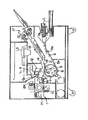
次に、上記4つの現像装置のうちの一つ、1Mについて図面を参照しながら説明する。なお、1M以外の現像装置も1Mと同様な構成となっているので説明を省略する。
【0077】
図2は、本発明の実施例に用いた現像装置1Mを示す構成図である。本現像装置は、図2に示すように、現像容器27を備える。現像容器27の内部は、隔壁29によって現像室(第1室)R1、と撹拌室(第2室)R2とに区画され、撹拌室R2の上方には隔壁29を隔ててトナー貯蔵室R3が形成され、該トナー貯蔵室R3内には補給トナー(非磁性トナー)28が収容されている。尚、隔壁29には補給口26が設けられ、該補給口26を経て消費されたトナーに見合った量の補給トナー28が撹拌室R2内に落下補給される。
【0078】
これに対し、現像室R1及び撹拌室R2内には現像剤19が収容されている。現像剤19は、粉砕法によって製造され、摩擦帯電量が約−2.0×10⁻²C/kg、平均粒径8μmの非磁性トナー(以下、単に「トナー」という)と、トナーに対して重量比で1%外添されている平均粒径20nmの酸化チタンと、0.1テスラに於ける磁化の値が2.7×105A/mの平均粒径35μmの磁性キャリアとからなる二成分現像剤である(磁性キャリアの混合比は、重量比で非磁性トナーが約7%になるようにした)。
【0079】
現像容器27の感光ドラム3に近接する部位には開口部が設けられ、該開口部から現像剤担持体としての現像スリーブ(非磁性円筒)21が外部に突出している。現像スリーブ21は現像容器27内に於いて回転可能に組み込まれており、本実施例に於いては、現像スリーブ21は、例えばSUS305ACのような、非磁性材からなり、その内部には磁界発生手段であるマグネットローラ(磁石)23が固定されている。
【0080】
磁石23は、現像磁極N1と、この現像磁極N1に対して現像スリーブ21の回転方向における上流側に位置する現像剤層厚規制極S3と、現像剤19を搬送するための磁極N2、S2、及び剥ぎ取り極S1とを有する。磁石23は、現像磁極N1が感光ドラム3に対向するように現像スリーブ21内に配置されている。現像磁極N1は、現像スリーブ21と感光ドラム3との間の現像部の近傍に磁界を形成し、該磁界によって現像スリーブ上に磁気ブラシが形成される。この位置に於いて、現像スリーブの回転と共に、矢印の方向に運ばれてきた現像剤は、感光ドラム3と接触し、感光ドラム3上の静電潜像は現像される。
【0081】
この時、現像スリーブ21と感光ドラム3の近接位置(現像部)に於いては、現像スリーブ21と感光ドラム3は互いに逆方向(カウンター方向)に移動する。N1極で現像を終了した現像剤は、S1、S3極により形成された反発磁界によって現像スリーブ上から剥ぎ取られ、現像室R1に落下する。現像磁極N1は、現像スリーブと感光ドラムの対向部に於いて、現像スリーブの回転方向で10°下流側に配置した。さらに、現像スリーブ上の現像剤の層厚を規制する規制手段としての規制ブレード18と略対向するようにS3極が配置されている。現像スリーブの直径は装置の小型化を考慮して10〜50mmのものを好適に用いることができ、本実施例では16mmのものを用いている。
【0082】
また、前述したように図3及び図4に示されるガウスメーターによって現像スリーブ21表面の磁界の強さを測定した。その結果、現像スリーブ21の中心方向を正としたとき、現像スリーブ21の法線方向の磁界の強さ(Br)の絶対値の自乗と、現像スリーブ21の接線方向の磁界の強さ(Bθ)の絶対値の自乗との和の、現像スリーブ21の法線方向に対する傾きのピーク位置(Frのピーク位置)は、前記最近接部に対して10°下流側にあり、Brのピーク位置は前記最近接部に対して5°下流側にあった(図5)。
【0083】
カウンター現像の場合、現像磁極N1を、現像スリーブと感光ドラムの対向部に於いて、現像スリーブの回転方向で上流側に配置すると、現像NIP(現像スリーブ上の磁気ブラシと感光ドラムとが接触する感光ドラム周方向の長さ)に搬送されてきた現像剤が現像スリーブの回転方向上流側(感光ドラムの回転方向では下流側)に於いて、現像剤が滞留し、キャリアが感光ドラムに付着してしまう現象が発生し易いので、本実施例では、現像磁極N1の位置を、現像スリーブと感光ドラムの最近接部と、最近接部よりも現像スリーブの回転方向下流側の15°の位置との間に位置するような構成としている。15°よりも更に現像スリーブ下流側に位置させると、現像剤が感光ドラムに非接触となり、はきよせ等のエッジ強調が目立ちやすくなってしまうからである。
【0084】
尚、現像スリーブには電源22により、交流電圧に直流電圧を重畳した振動バイアス電圧が印加される。潜像の暗部電位(非露光部電位)と明部電位(露光部電位)は、上記振動バイアス電位の最大値と最小値の間に位置している。これによって、現像部に、向きが交互に変化する交番電界が形成される。この交番電界中でトナーとキャリアが激しく振動し、トナーがスリーブ21及びキャリアへの静電的拘束力を振り切って潜像電位に対応した量のトナーが感光ドラム3に付着する。本実施例に於いては、感光ドラム3の暗部電位を−550v、明部電位を−100vとし、現像スリーブ21には直流バイアスとして、−300v、交流バイアスとして、Vpp2.0kV、Frq.6kHzの現像バイアスが印加されている。
【0085】
さて、現像スリーブ21の下方には、ブレード18が該現像スリーブ21と所定の間隔を於いて配置されている。現像スリーブ21とブレード18の間隔は、400μmである。ブレード18は現像容器27に固定されている。ブレード18は、鉄等の磁性材からなり、現像スリーブ21上の現像剤19の層厚を磁気的に規制する。
【0086】
現像室R1内には、搬送スクリュー24が収容されている。搬送スクリュー24は、羽根の直径が14mmのものを用いた。搬送スクリュー24は図中矢印が示す方向に回転され、該搬送スクリュー24の回転駆動によって現像室R1内の現像剤19は現像スリーブ21の長手方向に沿って全域で現像スリーブ21に向けて搬送される。本実施例に於いて、該搬送スクリュー24は、現像スリーブ21に対して、重力方向下部に配置される。その理由は、後述するが、搬送スクリュー24に収容される現像剤の最上面を現像剤層厚規制極と剥ぎ取り極の間に設定するからである。
【0087】
貯蔵室R2内には搬送スクリュー25が収容されている。搬送スクリュー25は、搬送スクリュー24と同じく羽根の直径14mmのものを用いている。搬送スクリュー25はその回転によって、トナーを現像スリーブ21の長手方向に沿った全域で撹拌しつつ搬送し、その末端で、十分に撹拌された現像剤を現像室R1へ受け渡す。なお、補給口26からは適当量のトナーが撹拌室R2内に自然落下する。
【0088】
次に、本実施例に於いて用いられる現像器の現像剤層厚規制極と、共に反発磁界を形成する剥ぎ取り極と、現像スリーブ近傍のスクリューの位置関係について、その作用も含めて詳述する。
【0089】
本実施例に於いては、反発磁界を形成するS3極とS1極のうち、S3極を現像剤層厚規制極として用い、S1極を現像剤剥ぎ取り極として用いる。S3極の現像スリーブ面に垂直な方向の磁界の強さBrのピーク値は0.04テスラ以上0.1テスラ以下、S1極のスリーブ面に垂直な方向の磁界の強さBrのピーク値は0.04テスラ以上0.08テスラ以下が好ましい。本実施例に於いては、S3極の磁界の強さのピーク値を0.06テスラ、S1極の磁界の強さのピーク値を0.05テスラとした。
【0090】
また、S3極とS1極の位置関係は、剥ぎ取り極S1の現像スリーブ面に垂直な方向の磁界の強さのピーク位置が、現像剤層厚規制極S3極の現像スリーブ面に垂直な方向の磁界の強さのピーク位置よりも重力方向で上部に位置するような構成を採っている。
【0091】
このような構成にすると、特別な剥ぎ取り手段を設けることなく現像後の現像剤が落下しやすく、現像剤層厚規制極による磁気的な吸引で現像剤を吸着し、現像部まで搬送しやすい。つまり、現像スリーブからの剤の剥ぎ取り、現像スリーブへの剤の供給に関して、簡易な構成にしやすい。
【0092】
また、S3極の現像スリーブ面に垂直な方向の磁界の強さのピーク位置と規制ブレードの先端(現像スリーブ側)とは、本実施例に於いては、5°(現像スリーブの中心位置を基)だけオフセット配置している。
【0093】
S3極は、S1極との間で反発磁界を形成しているので、S3極の磁力線は現像スリーブに対して、垂直に発散する傾向がある。その結果、現像スリーブに垂直な方向の磁界(磁力線密度)の変化率が小さくなる。
【0094】
そのことは、即ち、現像剤を現像スリーブに引き付ける力が小さくなることに相当する。このような構成をとると、現像剤が現像剤層厚規制極に於いて圧縮される力が弱まり、トナー劣化や、キャリアのスペント化といった現像剤の劣化が抑制され、現像剤寿命が延びることになる。しかしながら、本構成のように、反発磁界を形成する磁極のうちの一つの極を現像剤層厚規制磁極に用いる構成に限られるものではない。
【0095】
また、幾つかの検討の結果、前述した導電性磁性粉(103Ωcm以下の体積抵抗率をもつもの)による放電跡について、以下のようなことがわかった。すなわち、放電跡が線状に発生し、かつその放電跡が長く続くのは、現像スリーブと感光ドラムとの最近接部において、現像スリーブの回転方向上流側にて、導電性磁性粉が滞留することに起因することである。この滞留は、磁性キャリアの磁化が小さく、二成分現像剤の搬送力が弱い場合において発生しやすい。
【0096】
本実施例のような構成、すなわち磁性キャリアの磁化の大きさを比較的小さくし、現像スリーブと感光ドラムとがその最近接部において互いに逆方向に移動する構成を採った場合、現像極N1近傍の、現像スリーブ面に垂直な方向の磁界の強さ(Br)の絶対値の自乗と、現像スリーブ面上の接線方向の磁界の強さ(Bθ)の絶対値の自乗の和の、現像スリーブ面に垂直な方向への傾き(現像スリーブの中心に向かう方向を正(プラス)とする)のピーク位置を、現像スリーブと感光ドラムの最近接部に対して現像スリーブの回転方向下流側、特に0°〜15°(0°より大きく15°以下)に配置することにより、放電跡の連続的かつ線状に発生する頻度が激減し、また線状に発生した放電跡の最大長さも短くなった。
【0097】
なお、本実施例の構成で、現像容器内に直径が100μm以下で、体積抵抗率が103Ωcm以下の導電性磁性粉50mgを強制的に混入し、1000枚の耐久を行った結果、750枚から1000枚までの250枚中で、線状の放電跡は150個、最大の長さは50mmであった。
【0098】
以上のように、スリーブ面上で、スリーブ面に垂直に働く力Frは、Brの絶対値の自乗とBθの絶対値の自乗の和の、現像スリーブ面に垂直な方向の傾き(スリーブの中心に向かう方向を正(プラス)とする。)、即ち、現像剤に働く力のピーク位置を、現像スリーブと感光体の最近接部近傍であって、最近接部よりも現像スリーブの回転方向下流側15°以内の位置に配置することにより、現像スリーブ上を搬送されてきた導電性磁性粉が、そのピーク位置に引き付けられることにより、現像スリーブの回転方向上流側で滞留することがなく前記最近接部を通過する。
【0099】
その結果、放電跡が連続して、線状に発生する頻度が激減し、また、線状に発生した放電跡の最大長さも短くなった。なお、現像剤に働く力Frのピーク位置を15°以上更に下流側に位置させると、導電性磁性粉に対する力が及ばなくなり、滞留に対する効果は少なくなってしまった。
【0100】
<比較例>
本比較例では、実施例1の構成に対して、スリーブ面上で、スリーブ面に垂直に働く力Frは、Brの絶対値の自乗とBθの絶対値の自乗の和の、現像スリーブ面に垂直な方向の傾き(スリーブの中心に向かう方向を正(プラス)とする。)、即ち、現像剤に働く力、のピーク位置を、現像スリーブと感光体の対向部に対し、現像スリーブの回転方向上流側3°に配置した。その構成で現像容器内に直径100μm以下の導電性磁性粉50mgを強制的に混入し、1000枚の耐久を行った結果、750枚から1000枚までの250枚中で、線状の放電跡は、1500個、最大の長さは、140mmであった。
【0101】
【発明の効果】
本発明によれば、非磁性円筒上の導電性磁性粉は現像部よりも非磁性円筒の回転方向上流側(現像部入口側)で滞留することなく現像部(最近接部)を通過し、上記したような放電跡が発生するのを防止することができ、また万が一、放電跡が発生するようなことがあっても、その放電跡の連続発生、放電跡の発生頻度、放電跡の出現規模を抑制することができる。
【図面の簡単な説明】
【図1】本発明に係るフルカラー画像形成装置の一例を示す縦断面図である。
【図2】本発明の一実施例を示す現像器の概略図である。
【図3】Br測定方法を示す図である。
【図4】Bθ測定方法を示す図である。
【図5】現像スリーブ周方向に対するBθ、Br、Fθ、Frの強度分布を示す図である。
【図6】従来の現像器の一例を示す概略図である。
【符号の説明】
1 回転現像装置1
1M、1C、1Y、1Bk 現像器(現像装置)
3 電子写真感光ドラム(像担持体)
4 帯電器
5a、5b 給紙ガイド
6 給紙ローラー
7 グリッパ
8 当接用ローラー
9 転写ドラム
10 転写帯電器
12 クリーニング手段
13、14 除電器
15 分離爪
16 搬送ベルト
17 定着器(熱圧ローラ定着器)
18、33 規制ブレード
19 現像剤
21、30 現像スリーブ
22 電源
23 磁石(磁界発生手段)
24、25 搬送スクリュー
26 補給口
27、34 現像容器
28 補給トナー(非磁性トナー)
29 隔壁
31、32 撹拌スクリュー
35 マグネットローラー
50 ガウスメーター
51 アクシャルプローブ
C カセット
L レーザー光
LS レーザービームスキャナ
N1 現像磁極
N2、S2 磁極
R1 現像室(第1室)
R2 撹拌室(第2室)
R3 トナー貯蔵室
S1 剥ぎ取り極
S3 現像剤層厚規制極[0001]
BACKGROUND OF THE INVENTION
The present invention relates to a developing device that develops an electrostatic latent image formed on an image carrier, or a cartridge that has the developing device and is detachable from the image forming device, and more particularly to an image of a copying machine, a printer, a FAX, or the like. The present invention relates to a developing device or a cartridge used in a forming apparatus.
[0002]
[Prior art]
Conventionally, various apparatuses have been proposed and put into practical use as developing apparatuses used in an image forming apparatus using an electrophotographic system. Broadly divided, it can be divided into a developing device using a one-component developing system and a developing device using a two-component developing system. Most of the one-component developing methods are non-contact methods, and a typical developing method is a one-component jumping developing method using a magnetic toner.
[0003]
This developing method can obtain a high quality image with an easy configuration, but has a drawback that a color image cannot be obtained because the toner contains a magnetic material. In addition, the one-component development method using a non-magnetic toner can obtain a color image, but it is difficult to apply the toner on the developing sleeve, and it is currently coated with an elastic blade and is stable. There are aspects lacking in durability and durability.
[0004]
On the other hand, in the two-component development method, toner is transported to a development area by a magnetic carrier and development is performed. Usually, the development process is performed by bringing a developer into contact with a photosensitive drum. Here, the developing process will be described with reference to FIG.
[0005]
In the figure, 30 is a developing sleeve, 35 is a magnet roller fixedly arranged in the developing sleeve, 31 and 32 are stirring screws, 33 is a regulating blade arranged to form a thin layer of developer on the surface of the developing sleeve, 34 Is a developing container. Here, a developing process for visualizing the electrostatic latent image by the two-component magnetic brush method using the developing device and a developer circulation system will be described below. First, as the developing
[0006]
Here, when the developer formed in a thin layer is conveyed to the development main pole S1, a spike is formed by the magnetic force. The electrostatic latent image is developed with the spike-shaped developer, and then the developer on the developing
[0007]
A DC bias and an AC bias are applied to the developing sleeve from a power source (not shown). In general, in the two-component development method, by applying an AC bias, the development efficiency increases and the image becomes high quality.
[0008]
As a latent image forming method, an electrophotographic photosensitive member is scanned and exposed by a laser beam modulated in accordance with a recording image signal, and a dot distribution shape, that is, a dot-like latent image is distributed corresponding to an image. A method for forming a latent image is known. Among them, the so-called pulse width modulation (PWM) method that modulates the width (that is, the duration) of the laser drive pulse current in accordance with the density of the recorded image can obtain a high recording density (that is, high resolution). In addition, high gradation can be obtained.
[0009]
By the way, in recent years, further development of higher image quality and longer life using a two-component developing device has been promoted. Among them, in order to achieve a long life, it is necessary to take a configuration in which the developer is not compressed and to prevent deterioration of the toner and the carrier. One method for this is to reduce the magnetization of the magnetic carrier in the developer. The direction of decreasing the magnetization of the carrier is also the direction of improving the image quality in that the force for rubbing the toner image developed on the photosensitive member becomes weak in the developing unit.
[0010]
When the magnetization of the carrier is reduced and the developing sleeve and the photosensitive drum rotate in the forward direction, the above-mentioned advantages are provided, but there are also disadvantages. In the developing unit, the length of the magnetic brush is shortened, and the NIP (circumferential direction) where the developer is in contact with the photosensitive drum is narrowed, so that the density of the black solid rear end is increased. Emphasis will be noticeable.
[0011]
This phenomenon is caused when the developing sleeve and the photosensitive drum rotate in the forward direction at the opposite portion, and during black solid development, the developer is in contact with the photosensitive drum on the upstream side of the NIP where the developer contacts the photosensitive drum. The toner stays, and in the solid portion, development is poor, so that the toner does not adhere much on the photosensitive drum, and the staying toner adheres to the rear end (solid black) and occurs.
[0012]
When the magnetic brush length is long, the NIP in contact with the magnetic brush becomes long, no staying toner is generated, and the black solid trailing edge does not fray. Further, in the counter development in which the developing sleeve and the photosensitive drum are rotated in the opposite directions to each other, the stay on the photosensitive drum side on the upstream side of the NIP is eliminated, thereby reducing the magnetization of the carrier and shortening the magnetic brush length. Even so, it is difficult to generate edge enhancement such as hiding.
[0013]
The staying phenomenon that occurs in the forward direction occurs on the photosensitive drum on the upstream side of the NIP that is in contact with the magnetic brush in the rotational direction of the photosensitive drum (upstream in the rotational direction of the developing sleeve). However, in the counter development, since the developing sleeve and the photosensitive drum move in the opposite directions, the toner does not stay and is actually carried out of the NIP area by the rotation of the photosensitive drum. It will not stay.
[0014]
On the other hand, when the developing device is manufactured and assembled, the conductive magnetic powder may be mixed in the developing container. For example, when a developer container with a developing sleeve attached is covered with a lid to complete the developing device, when the lid is fixed to the developer container with a screw, the screw scraping powder between the screw and the bit insert That is, the conductive magnetic powder sometimes enters the developing container. In addition, conductive magnetic powder may adhere to clothes or work tools (for example, a driver) of an operator who assembles the developing container, and this may enter during the assembling of the developing container. As described above, the conductive magnetic powder sometimes enters in the process of manufacturing and assembling the developing device (developing container) and replacing the developing device (developing container).
[0015]
In addition, when a primary charger using a corona charging method is used to charge the photosensitive member to form an electrostatic latent image, the discharge wire of the primary charger is refreshed (discharge that adheres as it is used). In order to remove the product and improve the discharge efficiency), the conductive magnetic powder generated when the user or serviceman manually cuts the discharge wire or automatically cuts it into the developer container for some reason. It sometimes happened.
[0016]
However, when developing with the above-described configuration, that is, with the configuration in which the magnitude of the magnetization of the carrier is reduced and the developing sleeve and the photosensitive drum rotate in the counter direction with each other, the conductive in the developer container When the magnetic powder was mixed, discharge traces (marks) were continuously generated in a linear shape. And the maximum length of the trace of the discharge generated in this linear shape sometimes reached 700 mm.
[0017]
This discharge phenomenon is less likely to occur in series of discharge traces, and may occur independently one by one. Each discharge trace is white, with the middle being white and the surroundings being dark in the form of a ring or dark on the entire surface. It occurs in both solid white areas and solid black areas. When discharge traces are continuously generated in a linear shape, the discharge traces are conspicuous and the image quality is greatly reduced.
[0018]
[Problems to be solved by the invention]
An object of the present invention is to provide a developing device that can reduce the rate of occurrence of discharge traces even when conductive magnetic powder may enter the developing container.
[0019]
Another object of the present invention is to provide a developing device capable of shortening the maximum length even if discharge traces are generated linearly.
[0020]
Another object of the present invention is to provide a cartridge that can reduce the rate of occurrence of discharge traces even when conductive magnetic powder may enter the developing container.
[0021]
Another object of the present invention is to provide a cartridge capable of shortening the maximum length even if discharge traces are linearly generated.
[0022]
[Means for Solving the Problems]
The present invention includes a developer container that contains a developer including a non-magnetic toner and a magnetic carrier, a developer carrier that carries and transports the developer in the developer container,A power source for applying a developing bias to the developer carrying member;An electrostatic latent image formed on the image carrier by a magnetic brush formed on the developer carrier by the magnetic field generator. AndThe magnetization of the magnetic carrier is 3.0 × 10 in a magnetic field of 0.1 Tesla. 4 ~ 2.0 × 10 5 A / m,The moving direction of the image carrier and the developer carrier is opposite to each other at the closest portion between the image carrier and the developer carrier, and the surface of the developer carrierThe magnetic field generated by the magnetic field generating means in the tangential direction of B is Bθ, and the magnetic field generated by the magnetic field generating means in the direction perpendicular to the developer carrier surface is Br. The magnetic field is generated in the direction perpendicular to the developer carrier surface. The magnetic force Fr by the means is Fr = A · ∇r {(Br) 2 + (Bθ) 2 } (A is a constant), and the peak position of Fr is between the closest part and a
[0023]
DETAILED DESCRIPTION OF THE INVENTION
In the following embodiments, in the development of the electrostatic latent image, by defining the peak position of the magnetic force (magnetic attraction force) acting on the developer by the magnetic field generating means, the conductive magnetic powder is contained in the developing container. Even if this occurs, the rate of occurrence of discharge traces is reduced, and even when the discharge traces are generated linearly, the maximum length is to be shortened. The image forming method is not particularly limited as long as it is a method of performing a developer supplying step as described later, developing the electrostatic latent image formed on the image carrier with a two-component developer, and recording it on a sheet or the like. Alternatively, conventionally known image forming methods such as an electrophotographic method and an electrostatic recording method can be employed.
[0024]
As long as the image forming apparatus has at least characteristics such as the strength of a magnetic field generated by a magnetic field generation unit, which will be described later, various configurations conventionally known can be used. As such a configuration, a photoconductor (for example, an organic photoconductor) as an image carrier, a charging device (corona charger) for charging the image carrier, and an image to be formed on the charged image carrier (for example, An exposure apparatus for forming an electrostatic latent image corresponding to an image of a copy original), and an electrostatic latent image formed on the image carrier at the closest portion (developing unit) between the image carrier and the developer carrier A magnetic brush formed on the developer carrying member by the magnetic field generating means (a carrier spiked by a magnetic field is formed in a brush shape on the developer carrying member. The carrier carries toner, and this toner Development is performed by adhering to the electrostatic latent image on the image bearing member.) A developing device that contacts and develops the image bearing member, and a toner image obtained by the development is transferred to a transfer material such as plain paper Transfer device, heating the transferred unfixed toner image A fixing device for pressure and fixing can be exemplified a cleaning device for removing the toner remaining on the image bearing member after the transfer.
[0025]
The developing device includes a rotatable nonmagnetic cylinder (developing sleeve) as a developer carrying member, a magnet roller as a magnetic field generating means fixedly disposed inside the nonmagnetic cylinder, a developing container containing a two-component developer, At least. In the present invention, at the time of development, in the closest part (developing part), the moving directions of the non-magnetic cylinder and the image carrier carrying the electrostatic latent image are opposite to each other, that is, the opposite direction (counter direction). .
[0026]
The non-magnetic cylinder is preferably formed of a conductive material, such as a metal such as stainless steel or aluminum, a resin body imparted with conductivity by dispersing conductive particles, or the like. Various known materials can be exemplified. Further, the nonmagnetic cylinder may be subjected to processing such as roughening the surface by blasting or the like in order to improve the transportability of the two-component developer.
[0027]
The magnetic field generating means (magnet roller) has a plurality of magnetic poles (N pole and S pole) fixed inside the nonmagnetic cylinder so as to be relatively stationary with respect to the nonmagnetic cylinder. The magnetic field generating means may be a means such as a magnet that always generates a magnetic field, or may be a means such as an electromagnet that can arbitrarily generate a constant magnetic field or a magnetic field having a different polarity.
[0028]
In this embodiment, after development, a repulsive magnetic pole (S1, S3) of the same polarity for stripping off the developer from the developing sleeve is provided. Among the repelling magnetic poles, A regulating member (regulating blade) that regulates the layer thickness of the developer pumped up on the developing sleeve is disposed so as to substantially face each other. The developing sleeve is configured to convey the developer from the lower side to the upper side in the direction of gravity. By adopting such a configuration, it is possible to prevent the developer pumped up on the developing sleeve from being excessively compressed (applying an excessive load), so that the developer (especially the carrier) over a long period of time. Can be prevented from changing.
[0029]
In this embodiment, the peak position of the magnetic force Fr, which is a component in the direction perpendicular to the surface of the nonmagnetic cylinder (normal direction), of the magnetic force F (vector) by the magnetic field generating means at an arbitrary position on the surface of the nonmagnetic cylinder is In the vicinity of the closest part (development part), it is located downstream of the closest part in the rotational direction of the nonmagnetic cylinder. That is, if the tangential direction component of the magnetic field strength (also referred to as magnetic flux density) B (vector) of the magnetic field generating means at an arbitrary position on the nonmagnetic cylindrical surface is Bθ, the absolute value of Br and the absolute value of Bθ The peak position of the slope with respect to the direction perpendicular to the non-magnetic cylinder surface is the sum of the square of and the vicinity of the closest part (developing part), and is located downstream of the closest part in the rotational direction of the non-magnetic cylinder. ing.
[0030]
Further, the peak position of Br is also in the vicinity of the closest part (developing part) and is located downstream of the closest part in the rotational direction of the nonmagnetic cylinder.
Hereinafter, this reason will be described.
[0031]
The inclination of the sum of the square of the absolute value of Br and the square of the absolute value of Bθ with respect to the direction perpendicular to the surface of the nonmagnetic cylinder is determined by the magnetic field generating means fixed in the nonmagnetic cylinder. Represents the force (magnetic attraction force) for attracting the magnetic carrier carrying the toner.
[0032]
For one magnetic carrier, the magnetic force Fr (unit: N Newton) acting perpendicularly to the nonmagnetic cylindrical surface causes the magnetization of the magnetic carrier to be m (vector, unit of | m | is A / m), and magnetic carrier 1 V (mThree), Where the magnetic field strength by the magnet roller is B (B = (Br, Bθ)) and the direction toward the rotation center of the non-magnetic cylinder (developing sleeve) is the positive (plus) direction,
Fr = −A∇r (m · B)
= -Ad / dr (| m | VB · B)
=-| M | VAd / dr (B2)
=-| M | VAd / dr {(Br)2+ (Bθ)2}
It is expressed. Here, A is a constant, | m | is a function of magnetic permeability, and r is set in a radial direction (normal direction) with respect to the sleeve surface, so that the direction of the force is a force in a direction toward the center of the sleeve. It is.
[0033]
Therefore, the force Fr acting perpendicularly to the sleeve surface on the sleeve surface is the inclination of the sum of the square of the absolute value of Br and the square of the absolute value of Bθ with respect to the direction perpendicular to the developing sleeve surface (direction toward the center of the sleeve). Is positive (plus)).
[0034]
FIG. 5 shows an example of the intensity distribution of Br, Bθ, Fr, Fθ in the circumferential direction of the developing sleeve. The left vertical axis represents Gaussian (G), the right vertical axis represents intensity, and the unit is dimensionless (au). The horizontal axis represents the circumferential position of the developing sleeve, that is, the angle (the rotational direction of the developing sleeve is from left to right in FIG. 5). It means the closest part between the developing sleeve and the photosensitive member. As can be seen from FIG. 5, the peak position of Fr is located slightly downstream from the closest part (Sl / Dr facing part), and at this position, Fθ shifts from the plus side to the minus side. When Fθ is on the plus side, it means that a force to make the Fr peak reach the developer.
[0035]
As described above, the peak position of the inclination of the sum of the square of the absolute value of Br and the square of the absolute value of Bθ with respect to the direction perpendicular to the nonmagnetic cylindrical surface is in the vicinity of the developing unit (nearest portion). Even if the conductive magnetic powder as described above is mixed by being positioned downstream of the developing unit in the rotation direction of the nonmagnetic cylinder, it is conveyed toward the developing unit by the nonmagnetic cylinder. The conductive magnetic powder thus attracted is attracted to the peak position of Fr located downstream of the developing portion in the rotation direction of the nonmagnetic cylinder.
[0036]
Further, from FIG. 5, on the upstream side of the developing portion, the developer is subjected to a force for directing the Fr peak position by Fθ (force acting in the tangential direction of the sleeve surface with respect to the carrier (magnetic material)). Represents. That is, it is understood that the conductive magnetic powder is configured not to stay on the upstream side.
[0037]
Therefore, the conductive magnetic powder on the non-magnetic cylinder passes through the developing part (closest part) without staying on the upstream side of the non-magnetic cylinder in the rotation direction (developing part inlet side) with respect to the developing part. It is possible to prevent the occurrence of discharge traces. Further, even if a discharge trace occurs, it is possible to suppress the continuous generation of the discharge trace, the frequency of occurrence of the discharge trace, and the appearance scale of the discharge trace.
[0038]
The peak position of Fr is preferably set so as to be located between the closest part (developing part) and a position of 15 ° downstream of the closest part in the rotation direction of the nonmagnetic cylinder.
[0039]
If the Fr peak position moves further downstream than the position of 15 ° on the downstream side in the rotation direction of the non-magnetic cylinder, the action of force on the conductive magnetic powder is reduced, and the retention of the conductive magnetic powder is prevented. The effect may be insufficient. In the embodiment described below, since the diameter of the developing sleeve is 16 mm, the circumference of the developing sleeve between the closest portion and a position of 15 ° on the downstream side in the rotation direction of the nonmagnetic cylinder from the closest portion. The distance in the direction is about 2.1 mm.
[0040]
In this embodiment, the closest portion refers to a position where the surface of the nonmagnetic cylinder and the surface of the image carrier face each other at the smallest distance.
[0041]
The magnetic field strengths Br and Bθ can be measured by the method shown in FIGS.
[0042]
FIG. 3 is a diagram for explaining a method of measuring the magnetic flux density Br in the normal direction at an arbitrary position on the surface of the developing sleeve (nonmagnetic cylinder) 21, and the measurement is performed using a Gauss meter model 640 manufactured by Bell. In the drawing, the developing
[0043]
FIG. 4 is a diagram for explaining a method of measuring the magnetic flux density Bθ in the tangential direction on the surface of the developing
[0044]
The developing container described above may be a developing container that is suitably used to contain a two-component developer, and various conventionally known configurations can be used. The developing container is provided with a partition inside to form two or more storage spaces, one of the storage spaces is used as a space for supplying developer directly to the non-magnetic cylinder, and the other storage space is used as a new space. It is preferable that a space for supplying the developer is provided, and in each space, an agitating and conveying means for agitating and conveying the developer stored therein is suitably provided. The other space is preferably provided with a replenishing means for replenishing new non-magnetic toner as necessary.
[0045]
In the above description, the developing device used in the image forming apparatus has been described. However, the present invention is not limited to this, and the developing device may be unitized and the cartridge may be detachable from the image forming apparatus. In addition to the developing device, the cartridge may be configured to integrally include at least one of various devices constituting the image forming unit, that is, a photosensitive member, a cleaner, a primary charger, and the like.
[0046]
The nonmagnetic toner described above is not particularly limited as long as it is a nonmagnetic toner used for a two-component developer, and a known toner can be used. The non-magnetic toner is configured by using an appropriate amount of a binder resin such as a styrene resin or a polyester resin, a colorant such as carbon black, a dye or a pigment, a release agent such as wax, a charge control agent, or the like. Such a non-magnetic toner can be produced by a conventional method such as a pulverization method or a polymerization method.
[0047]
Non-magnetic toner (negative charging characteristics) has a triboelectric charge amount of −1 × 10⁻²~ -4.5x10⁻²It is preferably about C / kg. If the triboelectric charge amount of the non-magnetic toner is out of the above range, the development efficiency may be reduced and image defects may occur. The triboelectric charge amount of the non-magnetic toner may be adjusted according to the type of material used, or may be adjusted by adding an external additive described later.
[0048]
The triboelectric charge amount of the non-magnetic toner is the charge induced in the measuring container by using a general blow-off method, with the developer amount being about 0.5 to 1.5 g, and sucking the toner from the developer by air suction. It can be measured by measuring the amount.
[0049]
The nonmagnetic toner preferably has a volume average particle diameter of 4 to 15 μm. Here, for the volume average particle diameter of the nonmagnetic toner, for example, a numerical value measured by the following measurement method is used.
[0050]
A Coulter Counter TA-II type (manufactured by Coulter Inc.) is used as a measuring device, and an interface for outputting number average distribution and volume average distribution (manufactured by Nikka) and a CX-i personal computer (manufactured by Canon) are connected to the electrolyte Prepare 1% NaCl aqueous solution using primary sodium chloride.
[0051]
As a measuring method, 0.1 to 5 mL of a surfactant (preferably alkylbenzene sulfonate) is added as a dispersant to 100 to 150 mL of the electrolytic aqueous solution, and 0.5 to 50 mg of a measurement sample is further added.
[0052]
The electrolyte solution in which the sample is suspended is subjected to a dispersion treatment with an ultrasonic disperser for about 1 to 3 minutes, and a particle size distribution of 2 to 40 μm particles is measured using the 100 μm aperture as an aperture by the Coulter Counter TA-II type. Find the volume distribution. The volume average particle diameter of the sample is obtained from the obtained volume distribution.
[0053]
Conventionally known magnetic carriers can be used as the magnetic carrier. For example, a resin carrier formed by dispersing magnetite as a magnetic material in a resin and dispersing carbon black for conductivity and resistance adjustment. Alternatively, the surface of a magnetite single body such as ferrite that has been subjected to oxidation and reduction treatment to adjust the resistance, or the one that has been coated with a magnetite single body surface resin such as ferrite to perform resistance adjustment, or the like can be used. The method for producing these magnetic carriers is not particularly limited.
[0054]
The magnetic carrier is 3.0 × 10 in a magnetic field of 0.1 Tesla.FourA / m to 2.0 × 10FiveIt preferably has a magnetization of A / m. If the magnetization of the magnetic carrier is smaller than the above range, it is difficult to adhere to the non-magnetic cylinder by the magnetic field generating means, and image defects such as low image density may occur. Further, when the magnetization of the magnetic carrier is larger than the above range, the developer is compressed in the process of being conveyed by the nonmagnetic cylinder, and the developer may be deteriorated due to the compression.
[0055]
The volume resistivity of the magnetic carrier is 10 in consideration of leakage and developability.7-1014It is preferable to use one of Ωcm.
[0056]
The magnetization of the carrier was measured using an oscillating magnetic field type magnetic property automatic recording apparatus BHV-30 manufactured by Riken Denshi Co., Ltd. As the magnetic characteristic value of the carrier powder, an external magnetic field of 0.1 T is created, and the strength of magnetization at that time is obtained. The carrier is packed in a cylindrical plastic container so as to be sufficiently dense. In this state, the magnetization moment is measured, the actual weight when the sample is put is measured, and the magnetization strength is obtained (Am2/ Kg). Next, the true specific gravity of the carrier particles is determined by a dry automatic density Accupic 1330 (manufactured by Shimadzu Corporation), and the strength of magnetization (Am2/ Kg) is multiplied by the true specific gravity to determine the strength of magnetization (A / m) per unit volume used in the present invention.
[0057]
The magnetic carrier preferably has a weight average diameter of 20 to 100 μm, more preferably 20 to 70 μm. If the weight average diameter of the magnetic carrier is smaller than the above range, the transportability of the non-magnetic toner may be insufficient. If the weight average diameter is larger than the above range, the fluidity, chargeability and transportability of the two-component developer may be May be adversely affected.
[0058]
The weight average diameter of the magnetic carrier may be measured in the same manner as or in accordance with the particle size measurement of the non-magnetic toner described above, or sieves with different mesh sizes are stacked in order of increasing mesh size, You may put the sample which measured the weight, perform sieving, measure the residual amount on each net | network, and may measure by the sieving method displayed as an integrated percentage with the whole quantity.
[0059]
The two-component developer may contain other materials that are suitably used in addition to the non-magnetic toner and the magnetic carrier described above. Examples of such other materials include an external additive for controlling the fluidity and chargeability of the developer.
[0060]
The external additive has two effects in terms of hardware by coating the surface of the nonmagnetic toner and further on the surface of the nonmagnetic toner. One is that the fluidity is improved, and the replenishment toner is easily mixed and stirred with the two-component developer in the developing container. The other is that the external additive is present on the toner surface, so that the toner is developed. The release property of the non-magnetic toner supplied onto the photosensitive drum from the photosensitive drum is improved, and the transfer efficiency is improved.
[0061]
The external additive used in the present invention preferably has a particle size of 1/10 or less of the weight average diameter of the nonmagnetic toner particles from the viewpoint of durability when added to the nonmagnetic toner. The particle diameter of the external additive means the average particle diameter obtained by observing the surface of the toner particles with an electron microscope.
[0062]
As the external additive, various inorganic and organic compounds conventionally known as external additives can be used. For example, metal oxides (aluminum oxide, titanium oxide, strontium titanate, cerium oxide, magnesium oxide, Chromium oxide, tin oxide, zinc oxide, etc.), nitride (silicon nitride, etc.), carbide (silicon carbide, etc.), metal salt (calcium sulfate, barium sulfate, calcium carbonate, etc.), fatty acid metal salt
(Zinc stearate, calcium stearate, etc.), carbon black, silica and the like are used.
[0063]
The external additive is used in an amount of 0.01 to 10 parts by weight, preferably 0.05 to 5 parts by weight, based on 100 parts by weight of the nonmagnetic toner particles. The external additives may be used alone or in combination. Moreover, it is more preferable to use what each hydrophobized.
[0064]
【Example】
Embodiments of the present invention will be described below with reference to the accompanying drawings.
[0065]
FIG. 1 shows an electrophotographic color printer to which the present invention can be applied.
This printer includes an electrophotographic photosensitive drum (image carrier) 3 that rotates in the direction of an arrow. Around the
[0066]
In addition, when the wire of the charger using the corona charging method is deteriorated due to durability, a shaving member for refreshing the wire is provided to be slidable with respect to the wire at the longitudinal end portion (outside the charging region) of the wire. Yes.
[0067]
Each developing device contains a two-component developer containing toner particles having negative charging characteristics and carrier particles. The developer of the developing device 1M contains magenta toner, the developer of the developing device 1C contains cyan toner, the developer of the developing device 1Y contains yellow toner, and the developer of the developing device 1Bk contains black toner.
[0068]
The document to be copied is read by a document reading device (not shown). This reading device has a photoelectric conversion element for converting an original image such as a CCD into an electric signal, and outputs image signals corresponding to magenta image information, cyan image information, yellow image information, and black and white image information of the original, respectively. To do. The semiconductor laser built in the scanner LS is controlled according to these image signals and emits a laser beam L.
[0069]
An image can also be formed based on an image density signal from an electronic computer (such as a computer connected by a network cable).
[0070]
The sequence of the entire image forming unit will be briefly described by taking as an example the case of a full color mode for forming a full color image. Note that a mono color mode for forming a mono color image such as a black and white image and a mode for forming a two-color or three-color image can be selected by the control device (CPU).
[0071]
First, the
[0072]
A transfer material such as paper taken out from the cassette C and advanced through the paper feed guide 5a, the
[0073]
On the other hand, the
[0074]
The above process is performed on the yellow image signal and the black image signal, respectively, and when the transfer of the visible images (toner images) for the four colors is completed, the transfer material is neutralized by the
[0075]
This configuration is an example. For example, there are various methods such as the charger 4 being a charging roller instead of a corona charger, and the transfer charger 10 being a transfer roller. Thus, an image is formed through the steps of charging, exposure, development, transfer, and fixing.
[0076]
Next, one of the four developing devices, 1M, will be described with reference to the drawings. Since developing devices other than 1M have the same configuration as 1M, the description thereof is omitted.
[0077]
FIG. 2 is a block diagram showing the developing device 1M used in the embodiment of the present invention. The developing device includes a developing
[0078]
On the other hand, the
[0079]
An opening is provided in a portion of the developing
[0080]
The
[0081]
At this time, at a position close to the developing
[0082]
Further, as described above, the strength of the magnetic field on the surface of the developing
[0083]
In the case of counter development, when the developing magnetic pole N1 is disposed upstream of the developing sleeve and the photosensitive drum in the rotational direction of the developing sleeve, the developing NIP (the magnetic brush on the developing sleeve and the photosensitive drum come into contact with each other). The developer conveyed in the circumferential direction of the photosensitive drum) stays on the upstream side of the developing sleeve in the rotational direction (downstream side in the rotational direction of the photosensitive drum), and the carrier adheres to the photosensitive drum. In this embodiment, the position of the developing magnetic pole N1 is set to the closest position of the developing sleeve and the photosensitive drum, and the position of 15 ° downstream of the closest position to the rotation direction of the developing sleeve. It is set as the structure located between. This is because if the developer is positioned further downstream than 15 °, the developer is not in contact with the photosensitive drum, and the edge emphasis such as wiping becomes conspicuous.
[0084]
A vibration bias voltage in which a DC voltage is superimposed on an AC voltage is applied to the developing sleeve by a
[0085]
A
[0086]
A conveying
[0087]
A
[0088]
Next, the positional relationship between the developer layer thickness regulating pole of the developer used in this embodiment, the stripping pole that forms a repulsive magnetic field, and the screw in the vicinity of the developing sleeve, including its action, will be described in detail. To do.
[0089]
In this embodiment, of the S3 and S1 poles that form a repulsive magnetic field, the S3 pole is used as a developer layer thickness regulating pole, and the S1 pole is used as a developer stripping pole. The peak value of the magnetic field strength Br in the direction perpendicular to the S3 pole developing sleeve surface is 0.04 Tesla or more and 0.1 Tesla or less, and the peak value of the magnetic field strength Br in the direction perpendicular to the S1 pole sleeve surface is It is preferably 0.04 Tesla or more and 0.08 Tesla or less. In this example, the peak value of the magnetic field strength of the S3 pole was 0.06 Tesla, and the peak value of the magnetic field strength of the S1 pole was 0.05 Tesla.
[0090]
The positional relationship between the S3 pole and the S1 pole is such that the peak position of the magnetic field strength in the direction perpendicular to the developing sleeve surface of the stripping pole S1 is perpendicular to the developing sleeve surface of the developer layer thickness regulating pole S3. The configuration is such that the magnetic field is located above the peak position of the magnetic field strength in the direction of gravity.
[0091]
With such a configuration, the developer after development is easily dropped without providing any special stripping means, and the developer is attracted by magnetic attraction by the developer layer thickness regulating pole and easily transported to the developing unit. . That is, it is easy to make a simple configuration with respect to peeling off the agent from the developing sleeve and supplying the agent to the developing sleeve.
[0092]
In addition, the peak position of the magnetic field strength in the direction perpendicular to the S3 pole developing sleeve surface and the tip of the regulating blade (developing sleeve side) are 5 ° (the central position of the developing sleeve in this embodiment). Only the base) is offset.
[0093]
Since the S3 pole forms a repulsive magnetic field with the S1 pole, the magnetic field lines of the S3 pole tend to diverge perpendicularly to the developing sleeve. As a result, the rate of change of the magnetic field (magnetic line density) in the direction perpendicular to the developing sleeve is reduced.
[0094]
That is, the force for attracting the developer to the developing sleeve is reduced. With such a configuration, the developer compressing force at the developer layer thickness regulating pole is weakened, and the deterioration of the developer such as toner deterioration and carrier spent is suppressed, and the developer life is extended. become. However, the present invention is not limited to the configuration in which one of the magnetic poles forming the repulsive magnetic field is used as the developer layer thickness regulating magnetic pole.
[0095]
In addition, as a result of some studies, the above-described conductive magnetic powder (10ThreeThe following was found about the trace of discharge due to the volume resistivity of Ωcm or less. In other words, the discharge traces are linearly generated and the discharge traces continue for a long time. The conductive magnetic powder stays on the upstream side in the rotation direction of the developing sleeve at the closest portion between the developing sleeve and the photosensitive drum. It is due to that. This stagnation is likely to occur when the magnetization of the magnetic carrier is small and the conveying force of the two-component developer is weak.
[0096]
When the configuration as in this embodiment, that is, the configuration in which the magnitude of the magnetization of the magnetic carrier is made relatively small and the developing sleeve and the photosensitive drum are moved in the opposite directions at the closest portion, the vicinity of the developing pole N1 is adopted. The developing sleeve is the sum of the square of the absolute value of the magnetic field strength (Br) perpendicular to the developing sleeve surface and the square of the absolute value of the magnetic field strength (Bθ) in the tangential direction on the developing sleeve surface. The peak position of the inclination in the direction perpendicular to the surface (the direction toward the center of the developing sleeve is positive) is the downstream side in the rotation direction of the developing sleeve with respect to the closest portion of the developing sleeve and the photosensitive drum, in particular By arranging it at 0 ° to 15 ° (greater than 0 ° and 15 ° or less), the frequency of continuous and linear discharge traces is drastically reduced, and the maximum length of discharge traces generated linearly is shortened. It was.
[0097]
In the configuration of this example, the diameter in the developing container is 100 μm or less and the volume resistivity is 10ThreeAs a result of forcibly mixing 50 mg of conductive magnetic powder of Ωcm or less and performing durability of 1000 sheets, out of 250 sheets from 750 sheets to 1000 sheets, 150 linear discharge traces, the maximum length is It was 50 mm.
[0098]
As described above, the force Fr acting perpendicularly to the sleeve surface on the sleeve surface is the inclination in the direction perpendicular to the developing sleeve surface (the center of the sleeve) of the sum of the square of the absolute value of Br and the square of the absolute value of Bθ. ), That is, the peak position of the force acting on the developer is in the vicinity of the closest portion of the developing sleeve and the photoconductor, and downstream of the developing sleeve in the rotation direction of the developing sleeve. By arranging at a position within 15 ° on the side, the conductive magnetic powder conveyed on the developing sleeve is attracted to its peak position, so that it does not stay on the upstream side in the rotation direction of the developing sleeve. Pass through the tangent.
[0099]
As a result, the frequency of occurrence of discharge traces in a linear manner has been drastically reduced, and the maximum length of the discharge traces that have occurred in a linear fashion has also been shortened. Note that if the peak position of the force Fr acting on the developer is positioned 15 ° or more further downstream, the force on the conductive magnetic powder does not reach and the effect on retention is reduced.
[0100]
<Comparative example>
In this comparative example, the force Fr acting perpendicularly to the sleeve surface on the sleeve surface as compared with the configuration of Example 1 is the sum of the square of the absolute value of Br and the square of the absolute value of Bθ on the developing sleeve surface. Rotation of the developing sleeve with respect to the vertical position (the direction toward the center of the sleeve is positive (positive)), that is, the peak position of the force acting on the developer, with respect to the opposing portion of the developing sleeve and the photosensitive member Arranged 3 ° upstream in the direction. In this configuration, 50 mg of conductive magnetic powder having a diameter of 100 μm or less was forcibly mixed in the developing container, and as a result of durability of 1000 sheets, linear discharge traces were observed in 250 sheets from 750 sheets to 1000 sheets. 1500 pieces, the maximum length was 140 mm.
[0101]
【The invention's effect】
According to the present invention, the conductive magnetic powder on the nonmagnetic cylinder passes through the developing portion (closest portion) without staying on the upstream side in the rotation direction of the nonmagnetic cylinder (developing portion inlet side) from the developing portion, It is possible to prevent the occurrence of discharge traces as described above, and even if a discharge trace occurs, the occurrence of a continuous discharge trace, the frequency of occurrence of the discharge trace, the appearance of the discharge trace The scale can be suppressed.
[Brief description of the drawings]
FIG. 1 is a longitudinal sectional view showing an example of a full-color image forming apparatus according to the present invention.
FIG. 2 is a schematic view of a developing device showing an embodiment of the present invention.
FIG. 3 is a diagram showing a Br measurement method.
FIG. 4 is a diagram illustrating a Bθ measurement method.
FIG. 5 is a diagram illustrating intensity distributions of Bθ, Br, Fθ, and Fr with respect to the circumferential direction of the developing sleeve.
FIG. 6 is a schematic diagram illustrating an example of a conventional developing device.
[Explanation of symbols]
1 Rotating
1M, 1C, 1Y, 1Bk Developer (Developer)
3 Electrophotographic photosensitive drum (image carrier)
4 Charger
5a, 5b Paper feed guide
6 Paper feed roller
7 Gripper
8 Contact roller
9 Transfer drum
10 Transfer charger
12 Cleaning means
13, 14 Static eliminator
15 Separating nails
16 Conveyor belt
17 Fixing device (heat-pressure roller fixing device)
18, 33 Regulatory blade
19 Developer
21, 30 Development sleeve
22 Power supply
23 Magnet (magnetic field generating means)
24, 25 Conveying screw
26 Supply port
27, 34 Developer container
28 Replenishment toner (non-magnetic toner)
29 Bulkhead
31, 32 Stir screw
35 Magnet roller
50 Gauss meter
51 Axial probe
C cassette
L Laser light
LS laser beam scanner
N1 Development magnetic pole
N2, S2 magnetic pole
R1 Development chamber (first chamber)
R2 stirring chamber (second chamber)
R3 toner storage room
S1 Peeling pole
S3 Developer layer thickness limit
Claims (7)
像担持体上に形成された静電潜像を、前記磁界発生手段により前記現像剤担持体上に形成された磁気ブラシにより現像する現像装置において、
前記磁性キャリアの磁化は、0.1テスラの磁界において3.0×10 4 〜2.0×10 5 A/mであり、
前記像担持体と前記現像剤担持体との最近接部において前記像担持体及び前記現像剤担持体の移動方向は互いに逆方向であり、
前記現像剤担持体表面の接線方向における前記磁界発生手段による磁場の強さをBθ、前記現像剤担持体表面に垂直な方向における前記磁界発生手段による磁場の強さをBrとすると、前記現像剤担持体表面に垂直な方向における前記磁界発生手段による磁気力Frは、
Fr=A・∇r{(Br) 2 +(Bθ) 2 }
(Aは定数)
と表され、前記Frのピーク位置は、前記最近接部と、前記最近接部から前記現像剤担持体の回転方向下流側に15°離れた位置との間に位置することを特徴とする現像装置。A developer container containing a developer including a non-magnetic toner and a magnetic carrier; a developer carrier that carries and transports the developer in the developer container; and a power source that applies a development bias to the developer carrier; Magnetic field generating means provided in the developer carrying body for generating a magnetic field,
In a developing device for developing an electrostatic latent image formed on an image carrier by a magnetic brush formed on the developer carrier by the magnetic field generation unit,
The magnetization of the magnetic carrier is 3.0 × 10 4 to 2.0 × 10 5 A / m in a magnetic field of 0.1 Tesla ,
The moving directions of the image carrier and the developer carrier at the closest part between the image carrier and the developer carrier are opposite to each other,
When the strength of the magnetic field by the magnetic field generating means in the tangential direction of the surface of the developer carrier is Bθ, and the strength of the magnetic field by the magnetic field generator in the direction perpendicular to the surface of the developer carrier is Br. The magnetic force Fr by the magnetic field generating means in the direction perpendicular to the surface of the carrier is
Fr = A · ∇r {(Br) 2 + (Bθ) 2 }
(A is a constant)
The Fr peak position is located between the closest part and a position 15 ° away from the closest part downstream in the rotation direction of the developer carrier. apparatus.
Priority Applications (1)
| Application Number | Priority Date | Filing Date | Title |
|---|---|---|---|
| JP2001224603A JP4065481B2 (en) | 2000-07-31 | 2001-07-25 | Developing device and cartridge |
Applications Claiming Priority (3)
| Application Number | Priority Date | Filing Date | Title |
|---|---|---|---|
| JP2000-231750 | 2000-07-31 | ||
| JP2000231750 | 2000-07-31 | ||
| JP2001224603A JP4065481B2 (en) | 2000-07-31 | 2001-07-25 | Developing device and cartridge |
Publications (3)
| Publication Number | Publication Date |
|---|---|
| JP2002116626A JP2002116626A (en) | 2002-04-19 |
| JP2002116626A5 JP2002116626A5 (en) | 2004-12-16 |
| JP4065481B2 true JP4065481B2 (en) | 2008-03-26 |
Family
ID=26597064
Family Applications (1)
| Application Number | Title | Priority Date | Filing Date |
|---|---|---|---|
| JP2001224603A Expired - Fee Related JP4065481B2 (en) | 2000-07-31 | 2001-07-25 | Developing device and cartridge |
Country Status (1)
| Country | Link |
|---|---|
| JP (1) | JP4065481B2 (en) |
Cited By (1)
| Publication number | Priority date | Publication date | Assignee | Title |
|---|---|---|---|---|
| US9164417B2 (en) | 2012-05-14 | 2015-10-20 | Canon Kabushiki Kaisha | Image forming apparatus with developer bearing member velocity control |
Families Citing this family (4)
| Publication number | Priority date | Publication date | Assignee | Title |
|---|---|---|---|---|
| JP2005331632A (en) * | 2004-05-19 | 2005-12-02 | Canon Finetech Inc | Developing apparatus, process cartridge and image forming apparatus equipped with the same |
| KR100605170B1 (en) | 2004-07-19 | 2006-07-31 | 삼성전자주식회사 | Developing unit for image forming apparatus |
| JP2013152398A (en) * | 2012-01-26 | 2013-08-08 | Fuji Xerox Co Ltd | Development device and image forming apparatus using the same |
| JP6230448B2 (en) * | 2014-03-05 | 2017-11-15 | キヤノン株式会社 | Development device |
-
2001
- 2001-07-25 JP JP2001224603A patent/JP4065481B2/en not_active Expired - Fee Related
Cited By (1)
| Publication number | Priority date | Publication date | Assignee | Title |
|---|---|---|---|---|
| US9164417B2 (en) | 2012-05-14 | 2015-10-20 | Canon Kabushiki Kaisha | Image forming apparatus with developer bearing member velocity control |
Also Published As
| Publication number | Publication date |
|---|---|
| JP2002116626A (en) | 2002-04-19 |
Similar Documents
| Publication | Publication Date | Title |
|---|---|---|
| JP4860967B2 (en) | Development device | |
| JP2006284966A (en) | Image forming apparatus | |
| JP2010020281A (en) | Image forming apparatus | |
| JP2010002785A (en) | Image forming apparatus | |
| US6049687A (en) | Developing apparatus | |
| JP3437512B2 (en) | Developing device | |
| JP4065481B2 (en) | Developing device and cartridge | |
| US6421520B2 (en) | Developing apparatus having magnetic lower limit domain between repulsion magnetic fields | |
| US6704534B2 (en) | Developing device having minimum magnetic field strength adjacent regulating member | |
| US6539192B2 (en) | Developing device with developing mark reduction feature and cartridge using same | |
| JP2000194194A (en) | Developing device and image forming device provided therewith | |
| JP2004151358A (en) | Image forming apparatus | |
| JP2000010336A (en) | Image forming device | |
| JP2001281997A (en) | Developing device and image forming device | |
| JP2004219577A (en) | Developing device | |
| JP2002040811A (en) | Image forming device, image forming method and developing apparatus | |
| JP2002148941A (en) | Developing device | |
| JP2000250311A (en) | Developing device and image forming device | |
| JP3919374B2 (en) | Developing device and image forming apparatus | |
| JP2000194195A (en) | Developing device and image forming device provided therewith | |
| JP4689157B2 (en) | Development device | |
| JP2007240784A (en) | Image forming device | |
| JP2004021201A (en) | Developing device | |
| JPH08146757A (en) | Developing device | |
| JP2004191768A (en) | Developing device |
Legal Events
| Date | Code | Title | Description |
|---|---|---|---|
| A521 | Written amendment |
Free format text: JAPANESE INTERMEDIATE CODE: A523 Effective date: 20040106 |
|
| A621 | Written request for application examination |
Free format text: JAPANESE INTERMEDIATE CODE: A621 Effective date: 20040106 |
|
| A977 | Report on retrieval |
Free format text: JAPANESE INTERMEDIATE CODE: A971007 Effective date: 20060707 |
|
| A131 | Notification of reasons for refusal |
Free format text: JAPANESE INTERMEDIATE CODE: A131 Effective date: 20060919 |
|
| A521 | Written amendment |
Free format text: JAPANESE INTERMEDIATE CODE: A523 Effective date: 20061116 |
|
| TRDD | Decision of grant or rejection written | ||
| A01 | Written decision to grant a patent or to grant a registration (utility model) |
Free format text: JAPANESE INTERMEDIATE CODE: A01 Effective date: 20071218 |
|
| A61 | First payment of annual fees (during grant procedure) |
Free format text: JAPANESE INTERMEDIATE CODE: A61 Effective date: 20080105 |
|
| R150 | Certificate of patent or registration of utility model |
Free format text: JAPANESE INTERMEDIATE CODE: R150 |
|
| FPAY | Renewal fee payment (event date is renewal date of database) |
Free format text: PAYMENT UNTIL: 20110111 Year of fee payment: 3 |
|
| FPAY | Renewal fee payment (event date is renewal date of database) |
Free format text: PAYMENT UNTIL: 20120111 Year of fee payment: 4 |
|
| FPAY | Renewal fee payment (event date is renewal date of database) |
Free format text: PAYMENT UNTIL: 20130111 Year of fee payment: 5 |
|
| FPAY | Renewal fee payment (event date is renewal date of database) |
Free format text: PAYMENT UNTIL: 20140111 Year of fee payment: 6 |
|
| LAPS | Cancellation because of no payment of annual fees |