JP4065336B2 - High resolution spectroscopic microscopic method and apparatus - Google Patents
High resolution spectroscopic microscopic method and apparatus Download PDFInfo
- Publication number
- JP4065336B2 JP4065336B2 JP52350899A JP52350899A JP4065336B2 JP 4065336 B2 JP4065336 B2 JP 4065336B2 JP 52350899 A JP52350899 A JP 52350899A JP 52350899 A JP52350899 A JP 52350899A JP 4065336 B2 JP4065336 B2 JP 4065336B2
- Authority
- JP
- Japan
- Prior art keywords
- sample
- thermal
- thermal probe
- probe
- electromagnetic radiation
- Prior art date
- Legal status (The legal status is an assumption and is not a legal conclusion. Google has not performed a legal analysis and makes no representation as to the accuracy of the status listed.)
- Expired - Fee Related
Links
Images


Classifications
-
- G—PHYSICS
- G01—MEASURING; TESTING
- G01N—INVESTIGATING OR ANALYSING MATERIALS BY DETERMINING THEIR CHEMICAL OR PHYSICAL PROPERTIES
- G01N25/00—Investigating or analyzing materials by the use of thermal means
- G01N25/20—Investigating or analyzing materials by the use of thermal means by investigating the development of heat, i.e. calorimetry, e.g. by measuring specific heat, by measuring thermal conductivity
- G01N25/48—Investigating or analyzing materials by the use of thermal means by investigating the development of heat, i.e. calorimetry, e.g. by measuring specific heat, by measuring thermal conductivity on solution, sorption, or a chemical reaction not involving combustion or catalytic oxidation
- G01N25/4806—Details not adapted to a particular type of sample
- G01N25/4826—Details not adapted to a particular type of sample concerning the heating or cooling arrangements
- G01N25/4833—Details not adapted to a particular type of sample concerning the heating or cooling arrangements specially adapted for temperature scanning
-
- B—PERFORMING OPERATIONS; TRANSPORTING
- B82—NANOTECHNOLOGY
- B82Y—SPECIFIC USES OR APPLICATIONS OF NANOSTRUCTURES; MEASUREMENT OR ANALYSIS OF NANOSTRUCTURES; MANUFACTURE OR TREATMENT OF NANOSTRUCTURES
- B82Y35/00—Methods or apparatus for measurement or analysis of nanostructures
-
- G—PHYSICS
- G01—MEASURING; TESTING
- G01N—INVESTIGATING OR ANALYSING MATERIALS BY DETERMINING THEIR CHEMICAL OR PHYSICAL PROPERTIES
- G01N3/00—Investigating strength properties of solid materials by application of mechanical stress
- G01N3/60—Investigating resistance of materials, e.g. refractory materials, to rapid heat changes
-
- G—PHYSICS
- G01—MEASURING; TESTING
- G01Q—SCANNING-PROBE TECHNIQUES OR APPARATUS; APPLICATIONS OF SCANNING-PROBE TECHNIQUES, e.g. SCANNING PROBE MICROSCOPY [SPM]
- G01Q30/00—Auxiliary means serving to assist or improve the scanning probe techniques or apparatus, e.g. display or data processing devices
- G01Q30/02—Non-SPM analysing devices, e.g. SEM [Scanning Electron Microscope], spectrometer or optical microscope
-
- G—PHYSICS
- G01—MEASURING; TESTING
- G01Q—SCANNING-PROBE TECHNIQUES OR APPARATUS; APPLICATIONS OF SCANNING-PROBE TECHNIQUES, e.g. SCANNING PROBE MICROSCOPY [SPM]
- G01Q60/00—Particular types of SPM [Scanning Probe Microscopy] or microscopes; Essential components thereof
- G01Q60/58—SThM [Scanning Thermal Microscopy] or apparatus therefor, e.g. SThM probes
-
- G—PHYSICS
- G01—MEASURING; TESTING
- G01N—INVESTIGATING OR ANALYSING MATERIALS BY DETERMINING THEIR CHEMICAL OR PHYSICAL PROPERTIES
- G01N2203/00—Investigating strength properties of solid materials by application of mechanical stress
- G01N2203/02—Details not specific for a particular testing method
- G01N2203/026—Specifications of the specimen
- G01N2203/0286—Miniature specimen; Testing on microregions of a specimen
-
- Y—GENERAL TAGGING OF NEW TECHNOLOGICAL DEVELOPMENTS; GENERAL TAGGING OF CROSS-SECTIONAL TECHNOLOGIES SPANNING OVER SEVERAL SECTIONS OF THE IPC; TECHNICAL SUBJECTS COVERED BY FORMER USPC CROSS-REFERENCE ART COLLECTIONS [XRACs] AND DIGESTS
- Y10—TECHNICAL SUBJECTS COVERED BY FORMER USPC
- Y10S—TECHNICAL SUBJECTS COVERED BY FORMER USPC CROSS-REFERENCE ART COLLECTIONS [XRACs] AND DIGESTS
- Y10S977/00—Nanotechnology
- Y10S977/84—Manufacture, treatment, or detection of nanostructure
- Y10S977/849—Manufacture, treatment, or detection of nanostructure with scanning probe
- Y10S977/852—Manufacture, treatment, or detection of nanostructure with scanning probe for detection of specific nanostructure sample or nanostructure-related property
-
- Y—GENERAL TAGGING OF NEW TECHNOLOGICAL DEVELOPMENTS; GENERAL TAGGING OF CROSS-SECTIONAL TECHNOLOGIES SPANNING OVER SEVERAL SECTIONS OF THE IPC; TECHNICAL SUBJECTS COVERED BY FORMER USPC CROSS-REFERENCE ART COLLECTIONS [XRACs] AND DIGESTS
- Y10—TECHNICAL SUBJECTS COVERED BY FORMER USPC
- Y10S—TECHNICAL SUBJECTS COVERED BY FORMER USPC CROSS-REFERENCE ART COLLECTIONS [XRACs] AND DIGESTS
- Y10S977/00—Nanotechnology
- Y10S977/84—Manufacture, treatment, or detection of nanostructure
- Y10S977/849—Manufacture, treatment, or detection of nanostructure with scanning probe
- Y10S977/86—Scanning probe structure
- Y10S977/867—Scanning thermal probe
Landscapes
- Chemical & Material Sciences (AREA)
- General Physics & Mathematics (AREA)
- General Health & Medical Sciences (AREA)
- Physics & Mathematics (AREA)
- Health & Medical Sciences (AREA)
- Analytical Chemistry (AREA)
- Biochemistry (AREA)
- Life Sciences & Earth Sciences (AREA)
- Engineering & Computer Science (AREA)
- Immunology (AREA)
- Pathology (AREA)
- Nuclear Medicine, Radiotherapy & Molecular Imaging (AREA)
- Radiology & Medical Imaging (AREA)
- Combustion & Propulsion (AREA)
- Chemical Kinetics & Catalysis (AREA)
- Nanotechnology (AREA)
- Crystallography & Structural Chemistry (AREA)
- Investigating Or Analyzing Materials Using Thermal Means (AREA)
Description
技術分野
本発明は不均質なサンプルの個々の部分の分光分析に関する。分析すべき領域は走査型プローブ顕微鏡を用いることにより高空間分解能で識別され、選択され、そしてその像が形成される。
背景技術
アーモンド(D.P.Almond)およびパテル(P.M.Patel)が『光熱科学および技術(Photothermal Science and Techniques)』(Chapman Hall(London and New York,1996))で発表している固体や薄いフィルムの光熱特性を分析する技術が広く用いられている。近年、これら技術に空間分解能を加えられることは様々な分野で技術的な関心事となっている。その一例は電子光学装置の一般分野である。しかしながら殆どの市販の方法には用いる検出システムの光学波長が有限であることから制限を受ける点で問題がある。例えば実際には人気はあるが高価なフーリエ変換赤外顕微鏡技術における空間分解能は5〜10マイクロメータ以下である。
熱像を形成するための従来の多くの方法は小さな光源から発せられ、そして回折の法則に従って広がるエネルギビームを用いる。この広がりの程度は通常はエネルギ束に関連した波長により決まる。しかしながらサンプルが近視野領域内にあるとき、すなわち光源から一波長よりもかなり近いときにはビームの直径を非常に小さくできる。事実、サンプルが光源から一波長も離れていないときにはビームの直径は光源自身の大きさよりさほど大きくはない。この原則は走査プローブ顕微鏡において当てはまる。走査プローブ顕微鏡では尖ったプローブがサンプル表面近くに配置される。そしてプローブとサンプルとの相互作用が生じる。プローブがサンプル表面上を走査する間、この相互作用が監視される。そして像コントラストがコンピュータにより形成される。この像コントラストは走査域におけるサンプルでの幾つかの特性(例えば物理的、機械的、化学的特性)の違いを表している。このような走査プローブ顕微鏡の一つに原子間力顕微鏡(AFM)がある。従来の原子間力顕微鏡では走査されている表面上方のプローブの高さをフィードバックシステムにより制御する。このフィードバックシステムはプローブとサンプルとの間の力を一定に維持する。プローブの高さが監視され、データが提供され、このデータが走査域の形状を表す像コントラストを形成するのに用いられる。
走査プローブ顕微鏡システムの一部として小型の熱電対プローブとその他の近視野装置とを用いることにより回折に起因する制限を克服できるので例えばウィリアムズ(C.C.Williams)およびウィックラマシンジ(H.K.Wickramasinghe)が『光音響理論および光熱理論(Photoacoustic and Photothermal Phenomana)』(P.Hess and J.Petal(eds)Springer(Heidelberg,1988))で発表しているような近視野走査光熱分光計が調査技術として認識されるようになった。これら装置ではプローブは熱電対同志を非常に微細な形態で接合する特別に作製された同軸先端部品である。このプローブは数十ナノメータ単位の空間分解能を提供した。サンプルはレーザまたはプローブを用いて加熱されるか、或いはサンプルは電気的に加熱される。フィードバックシステムは必要に応じてプローブの高さを変えることで(力を一定に維持する代わりに)プローブ温度を一定に維持する。ウェーバ(J.M.R.Weaver)、ウォルピタ(L.M.Walpita)およびウィックラマシンジは(一つの単電導体で形成された)走査トンネル顕微鏡プローブと電導体サンプルとを接触することにより熱電対が接合される点を除いて上記ウィリアムズおよびウィックラマシンジの研究に類似した研究を『Nature Vol342』(pp.783-5(1989))に発表している。彼らはこの機構を用いてナノメータ単位の空間分解能を備えた吸光顕微および分光を実行した。得られた像のタイプとしては表面形状の違いに応答した電子トンネル像と、サンプル−基板系での吸光特性および熱特性の違いに応答した熱像とである。
『Soc.Photo.Instrum.Engrs.Vol.897』(pp.129-134(1988))で公表された他の論文においてウィリアムズおよびウィックラマシンジは電子ビームにより発生せしめられた格子構造において光熱的に引き起こされた温度の違いを計測するのに近視野熱プローブを受動モードで用いた。彼らは近視野熱・光熱顕微鏡には準光学的な水平分解能での吸光分光計における応用や小さいスケールでの発熱・吸熱過程を測定するための応用があると提案した。
当該分野における更なる開発が『Microelectronic Engineering Vol.24』(pp.107-112(1994))においてオエスターシュルツ(E.Oesterschulze)ソプカ(M.Stopka)およびカッシング(R.Kassing)により発表され、マジュンダ(A.Majumdar)、ロウ(K.Lou)、シー(Z.Shi)およびバレシ(Varesi)は『Experimental Heat Transfer vol.9』(pp.83-103(1996))においてこの分野を追試した。またマジュンダ他は『Appl.Phys.Lett.vol.62』における『原子間力顕微鏡を用いた熱像形成(Thermal Imaging Using the Atomic Force Microscope)』(pp.2501-3(1993))でウィリアムズおよびウィックラマシンジにより発表された熱電対よりも単純な構造の熱電対を用いる熱像形成技術を発表している。また彼らは先端部とサンプルとの接触を維持するために標準的な原子間力顕微鏡のフィードバックを実行した。
ディンウィディ(R.B.Dinwiddie)、ピルキー(R.J.Pylkki)およびウエスト(P.E.West)は『Thermal Conductibity 22』における『走査熱顕微鏡を用いた熱伝導率コントラスト像形成(Thermal Conductivity Contrast Imaging with a Scanning Thermal Microscope)』(T.W.Tsong(ed.)(1994))で極めて小さいプラチナ抵抗温度計の形をしたプローブを用いることを発表している。またピルキー(Pylkki)他の米国特許第5,441,343号('343特許)は走査プローブ顕微鏡に用いるための熱検出プローブを開示しており、ここではプローブがサンプル表面上を走査せしめられる間においてプローブの接触力が一定レベルに維持される。
また他の関連技術は走査熱顕微鏡で実行される熱分析により局部的な化学的指紋をとるために近年開発された技術である。これは米国特許第5,248,199号('199特許)および米国特許出願第08/837,547号('547出願)に記載されている。なおこれら両文献は本願の一部を構成する。これは以下の刊行物にも掲載されている。すなわちハミッチ(A.Hammiche)、ポロック(H.M.Pollck)、ソング(M.Song)およびホルストン(D.J.Hourston)の『Measurement Science and Technology 7』(142-150(1996))、ハミッチ、ポロック、ホルストン、リーディング(M.Reading)およびソングの『J.Vac.Sci.Technol.B14』(1486-1491(1996))、ハミッチ、リーディング、ポロック、ソングおよびホルストンの『Rev.Sci.Instrum.67』(4268(1996))、ホロック、ハミッチ、ソング、ホルストンおよびリーディングの『Journal of Adhesion,Vol.67』(pp.193-205(1998))である。この発明は小型の抵抗熱プローブを用いた物質の熱特性の計測に関し、特に従来では数ミリメータ四方単位の体積の物質から容積の熱量データを得ていたが数ミクロン四方単位の体積の物質からでも熱量情報を得ることができる局部熱分析実験の実行に関する。またこの作業の間に熱波動を用いて表面下の深さの輪郭形成と像形成とを実行する手段が開発された。
この発明の他の特徴は消えていく熱波を研究対象の物質内に生成するためにプローブ温度を変調し、表面下の像を形成することに関する。これによりリーディング(Reading)他の米国特許第5,224,775号('775特許)に記載されているサンプル物質の容積熱分析実験を行うのに従来用いられてきた変調示差熱走査熱量計の技術をTopometrix社(Topometrix Corporation)により開発され且つ上記'343特許に記載された極めて小型の二つの抵抗プローブを示差の形態で用いる顕微鏡に応用することが可能となった。走査プローブ顕微鏡に取り付けられたサンプル用プローブは視野の範囲にある表面上の所望の場所に配置される。局部的な相転移を引き起こし、そしてこれを検出することによりその場所で局部熱量測定が実行される。このことはプローブ温度に勾配をつけることにより達成される。またプローブに変調された電流を加えることにより温度勾配に小さい温度振動が加えられる。特定の場所のサンプル熱特性の像を形成するためにサンプル表面上を走査することによりサンプル上の特定の場所に対応したコントラストが形成される。
Topometrix社により開発されたプローブは片持ち梁の形をした長いループ状のウォルストンワイヤ(Wolaston wire)であり、この端部は抵抗要素を形成する。この要素の抵抗は温度で変わる。逆にこの抵抗要素に適量の電流を通すことで温度を設定することができる。従来の原子間力顕微鏡でそうしているようにループを横断してミラーを取り付けられ、プローブがサンプル表面上を走査している間にサンプル上の抵抗要素の接触力を一定に維持できるようにする。
プローブは該プローブに電流を通すことで非常に局部的な加熱源として用いられる。プローブの温度は一定および/または時間で変わるように設定される。プローブをサンプル表面に近づけると熱がプローブからサンプルに流れる。熱流量はプローブの下側の位置におけるサンプルの様々な特性に従って変わる。この熱流量の変化により抵抗要素の温度が変化せしめられ、その抵抗値が変化する。なおプローブの抵抗値変化(すなわち温度変化)を検出し、プローブを流れる電流の量を増加し、そして抵抗値を元の抵抗値(すなわち設定温度)に戻すためにフィードバック回路を用いることが好ましい。
次いで直接または固定型増幅器により示差信号が監視される。示差信号は(1)温度に対して振幅および位相データの局所分析プロットを実行し、サンプルの特定位置の熱量情報を提供するか、または(2)走査域での熱伝導率および/または熱拡散率の違いを表しているコントラストを有する像を構築するのに用いられる。第二の実施例では抵抗要素を通る時間に応じて変化する電流がサンプル内に熱波を生成する。この時間に応じて変化する電流の変調周波数は機能的には所望のサンプル像が位置するサンプル表面下方の深さに関連する。こうして表面下の像が形成される。像に与えるサンプル表面下の物質の深さは温度変調周波数を適切に選択することにより制御される。アルモンド(Almond)他が『Photothemal Science and Techniques』(page 15,Chapman and Hall(London 1996))で発表しているように浸透深さは適用された熱波の振動により分割されるサンプルの熱拡散率の平方根に比例する。なおこの内容は本願の一部を構成する。
本発明は化学的指紋技術を拡大し、真の化学分析を提供できるという点で利点がある。近視野顕微鏡と組み合わせた吸光分光上の上記作業は電気伝導性サンプルの研究に制限され、または照射光の個別の波長の使用に制限されてきた。さらに局部分光分析の鍵となる赤外線吸収における局部変化から熱特性における空間的な変化のノイズを除去するための信頼できる方法は発表されていなかった。したがって今のところ高空間分解能での分光による化学分析に適用された上記技術の報告はなく、このことが本発明が関連する主題である。なお本願で参照する刊行物、特許および特許出願は本願の一部を構成する。
発明の開示
本発明によれば赤外分光計用の検知装置としてサンプルおよび走査プローブ顕微鏡を使用することより高空間分解能の分光計像が得られる。これにより従来の赤外顕微鏡の回折制限が克服され、分光像に大きく改善された空間分解能(潜在的には数十ナノメートル程度)を提供する。
赤外分光計からのビームがサンプルに向けられる。サンプルはそれが赤外放射を吸収する程度、すなわち個々の領域の結果的な温度上昇が具体的な分子種の存在(および赤外線の波長範囲)に依存する程度まで加熱される。これら個々の温度差は小型の熱プローブにより検出され、計測される。熱プローブは走査熱顕微鏡内に設置される。そして走査熱顕微鏡はサンプルの多数の表面の像および表面下の像を形成するように作動せしめられる。像のコントラストは物質表面での熱拡散、表面形状、化学組成またはその他の特性の違いに相当する。
本発明の目的はサンプルの走査熱顕微鏡像を得ることにあり、ここでの像のコントラストはサンプルがさらされる赤外放射(または他の電磁放射)から吸収した熱量の違い、すなわち化学組成の違いにより決まる。
本発明の別の目的は分光的にサンプルの個々の領域を分析することにある。なお熱プローブを用いて、または別の方法を用いて得られる走査プローブ像から像を選択することができる。
本発明の別の目的は局所分光分析の鍵である赤外線吸収に起因する局部間の熱的な違いから熱特性における空間的違いのノイズを除去することにある。
本発明の別の目的は小型の温度検出プローブを用いて電磁放射にされされたサンプルの熱吸収速度を測定することにある。
本発明の別の目的は電磁スペクトルの赤外線領域内で選択された帯域に制限された波長の放射を用いて回折の制限のない高空間分解能で分散的な赤外顕微を実行することにある。
本発明の別の目的は濾過されていない広帯域の放射を用いて回折の制限のない高空間分解能でフーリエ変換赤外顕微を実行することにある。
本発明の別の目的は(温度を検出し、上記目的で挙げた機能を実行するのに加えて)点加熱源として機能する抵抗熱プローブを提供することにあり、これによれば選択した個々の場所で分光分析されている物質の容積を使用者が選択するのに必要な高周波数温度変調が提供される。
【図面の簡単な説明】
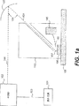
図1aはフーリエ変換赤外線分光計を用いる本発明の全体構成の概略図である。
図1bはデュアル出力ビーム型のフーリエ変換赤外線分光計を用いる本発明のブロック線図である。
図1cは単色放射源を用いる本発明のブロック線図である。
図1dは電磁放射を提供するために分光計を用いる本発明のブロック線図である。
図2はヘリウム−ネオンレーザから可視光を照射したシリコン/二酸化シリコン格子の光熱像である。
図3は図1に示したシステムを用い、0.051cm/秒のミラー速度で且つ16cm-1の分解能で得られたポリスチレンサンプルのインターフェログラムである。
図4は従来のフーリエ変換赤外分光計を用いて得られたスペクトル(上側の線)と図3のデータを変換して得られたスペクトル(下側の線)とを比較した図である。
発明を実施するための最良の形態
図1aのように本発明の第一の実施例はフーリエ変換赤外分光計(FTIR)の赤外源101および干渉計102を用いる。干渉計102はマイケルソン干渉計(Michelson interferometer)またはフーリエ変換赤外分光計に適した他のタイプの干渉計である。変調されていないビーム103は干渉計102により変調される。赤外線ビームは変調されたビーム104として干渉計102から出る。ビーム104はミラー105により走査熱顕微鏡110内のステージ108上に配設されたサンプル106の表面上に向けられる。赤外ビームが照射されたサンプル上の位置と同じ位置のサンプル106上に熱プローブ100の先端部107が配置される。モジュール109が上記'547出願に記載されているように熱プローブの温度および電流を制御し、そして計測し、また熱プローブの位置を制御する。プローブ100は受動的なプローブまたは能動的なプローブである。いずれの場合においても実行せしめられる測定が特性における示差となるように同じタイプの第二のプローブが基準プローブとして用いられる。
典型的な受動タイプのプローブは受動モードで用いられるウィックラマシンジ(Wickramasinghe)、マジュンダ(Majumdar)またはウェーバ(Weaver)により記載されているような熱電対プローブ、または上記'547出願あるいは上記'343特許に記載されているウォラストン(Wollaston)タイプの抵抗プローブのような小型温度計のみである。
能動タイプのプローブは温度計およびヒータの両方として用いられる。これには上記'547出願または上記'343特許に記載されているウォラストンタイプの抵抗プローブが用いられる。
例えば走査熱プローブ顕微鏡110はマジュンダにより上記'199特許および上記'547出願に記載されている。
図1bはデュアルビーム型干渉計を用いて実行される本発明の第一実施例のブロック線図である。ここでは干渉計112の出力は二本の出力ビーム114である。ビーム114Sは熱プローブに接触しているサンプルに向けられる。ビーム114Rは熱プローブに接触している対照に向けられる。モジュール119は熱プローブの温度を制御し、そして測定するために電気回路およびその他のハードウェアならびにソフトウェアを有する。熱プローブは出力信号が基準プローブに対するサンプルプローブの温度差を表す示差信号となるように示差の形態で接続される。
図1cに示したように電磁放射源131は単色のレーザまたは調整可能なレーザである。ビーム132が変調されているのが好ましく、すなわち電磁放射源131が変調電磁放射源であるのが好ましい。ビーム132はビームスプリッタ133によりサンプルビーム132Sおよび基準ビーム132Rそれぞれに分割される。フーリエ変換赤外分光計の実施例のようにサンプルビームはサンプル用の熱プローブの位置と同じ位置でサンプル134Sの表面に照射される。一方、基準ビーム132Rは対照用の熱プローブの位置と同じ位置で対照の表面に照射される。次いでサンプル電気信号と基準電気信号とが熱プローブモジュール136に入力され、そしてモジュール136は温度差信号を出力する。なお対照に対してサンプルからの示差信号を直接的に表している電気的な示差信号を発生するようにサンプル用の熱プローブと対照用の熱プローブとを電気的に接続してもよい。いずれの場合においても示差信号はサンプルが熱プローブに対して走査される間(または熱プローブがサンプルに対して走査される間)に像コントラストを提供するのに用いられる。
図1cの装置を基準ビームなしで作動するように修正することもできる。この場合にはビームスプリッタ133は用いられず、一本のビームがサンプル上の一つの熱プローブに向けられ、そしてサンプルのデータを記録し、基準データを記録するために第二の計測が実行される。次いで対照に対するサンプルの空間走査が実行されている間に像を提供するために基準データに対するサンプルデータの比(またはサンプルデータから基準データを引いた値)が熱プローブに対するサンプルの各位置について算出される。
図1dは本発明の分光装置を用いた時のブロック線図である。ここでの分光装置はビーム142を波長選択器および変調器143(モノクロメータおよびチョッパー、音響光学変調器あるいは光電子変調器を備えた調整可能なフィルタ、調整可能な液晶フィルタまたはホログラフィックフィルタ等)に向ける光源141を具備する。
作動モード
本発明を実施する一つの好適なモードではサンプルがさらされる赤外放射またはその他の電磁放射から吸収される熱量の違いから像コントラストが得られ、この像コントラストは表面での化学組成の違いを示している。走査熱顕微鏡をサンプル上に配置し、像をとるべきサンプルの範囲に放射の焦点を合わせる。サンプル上の或る点から別の或る点での温度の違いは吸収係数、熱伝達率および熱拡散率の違いで決まる。放射の入射強度は機械式チョッパーまたは上述した別のタイプの変調器の一つにより変調される。次いで能動タイプの熱プローブをサンプルに接触するように配置し、プローブとサンプルとの間の接触力を原子間力顕微鏡での標準的な手順である原子間力フィードバック制御により設定する。次いで熱プローブおよび赤外線ビームでサンプルを走査し、そして像コントラストが温度計として働いているサンプル用の熱プローブからの信号と対照用の熱プローブからの信号との差により決まる。この場合、全ての生データは差を表す測定値の形をとる。この装置は電磁放射にさらされたサンプルに吸収される熱の吸収速度を計測するのにも用いられる。
このような像コントラストの例を図2に示す。図2はヘリウム−ネオンレーザから可視光を照射したシリコン/二酸化シリコン格子の光熱像である。能動モードで用いられる抵抗熱プローブにより明らかであるが像のコントラストは二つの異なる材料のヘリウム−ネオンレーザの吸収率に差があることに起因して二つの材料の二つの異なる温度への異なる加熱から生じる。
本発明は回折の制限のない高分解能でのフーリエ変換赤外分光装置にも用いられる。フーリエ変換赤外分光は濾過されていない広帯域の放射を用いる。走査熱顕微鏡を分析すべきサンプルの範囲上に配置し、上述した原子間力フィードバックの下でプローブを接触させる。ビームの焦点を合わせ且つビームを方向付ける図1aに示した装置を用いてフーリエ変換赤外分光計からの赤外線の焦点をプローブとサンプルとの間の接触点に合わせる。赤外線は干渉計で変調される。これにより官能基による吸収に起因してサンプルが局所的に加熱される。発生せしめられた熱波を受動モードで用いるプローブにより直接検出する。プローブの熱時定数はプローブが干渉計による変調に応答できるように十分に短い。この熱時定数はサンプルではなくプローブ自体が赤外線ビームにより直接どの程度加熱されたかに依存する。基礎技術は赤外光音響分光計の技術と同様である。出力信号および対照用のプローブから差の形で得られた熱インターフェログラムは赤外線ワークステーションに保存される。インターフェログラムはフーリエ変換赤外分光計で変換されるように変換され、周波数スペクトルが提供される。
短い熱時定数と高空間分解能を提供するように選択された小型の熱プローブにより幾つかの場合では標準の赤外分光計に比べてノイズに対する信号の割合が比較的小さくなる。この場合、繰り返し実行するデータ走査を平均化することが必要となる。個々の走査が弱くてインターフェログラムの凸部がノイズレベルより低いとフーリエ変換赤外分光データの平均化に一般的に用いられている動的整列理論は役に立たない。しかしながらこの状況においてもフーリエ変換装置が個々の走査の凸部の認識に依存しない絶対的な基準に対して走査を整列するタイプであれば連続した走査が平均化される。
この方法により得られるインターフェログラムの例は図3に示されており、最終的に処理されたスペクトルは図4の下側の線で示されている。Sで示されているピークはライン周波数ノイズから生じている。残りのピークは図4の上側の線で示した標準的なフーリエ変換赤外分光計の走査から得られるスペクトルで示されるピークと一致している。
本発明はサンプルの個々の範囲における分光分析を実施するのに用いられ、該サンプルは同じ熱プローブの使用で得られる走査プローブ像から選択される。サンプルは上述したようにフーリエ変換赤外分光計に接続された走査プローブ顕微鏡によりその像を形成される。プローブは能動モードで用いられ、非変調熱像および変調熱像の両方が得られ、形状の像に加えて異なる組成面(化学的または組成的)を区別できる。次いで上記(3)での測定のように実行される赤外線測定を所望する点に上記'547出願に記載されているようなコンピュータ制御の下でプローブを再び位置決めする。この場合では像の空間分解能はプローブ先端部の寸法、プローブ応答時間定数、サンプルの熱拡散速度、サンプルの吸光深さおよび干渉計の変調周波数により決まる。
図1dに示した本発明の実施例では照射される電磁放射の波長はモノクロメータやフィルタを用いて電磁スペクトルの赤外範囲内の選択された帯域に制限される。スペクトルを得るためにデータをフーリエ変換することはないが装置の作動は本発明のフーリエ変換赤外分光計の実施例に対して上述した作動と同様である。このことは光音響分光計の確立された原理に基づいた計算により確かめられる。
走査用熱プローブで用いられるタイプの熱プローブの温度感度は10mKより高い。本発明の実験条件下では算出された温度上昇値は添付資料Aに要約されているように興味のある別の多数の場合においてこの値を越える。これら計算は実際に得られるビームフラックス値を考慮し、多くの高分子材料では典型的な熱特性および吸収特性を有するサンプルに当てはまる。またこれら計算はサンプルの表面付近の領域が(i)熱的に厚く、光学的に不透明である場合、(ii)熱的に厚く、光学的に透明または光学的には不透明であるが光熱的に透明である場合、(iii)光学的に透明で熱的に薄い場合を考慮している。
本発明を実施するその他のモードは熱を検出し且つ上記目的に挙げた機能を実行するのに加えて点加熱源として機能する抵抗熱プローブを提供することにある。これにより使用者が(a)選択された個々の局部において分光分析される物質の体積を選択するため、そして(b)局部間での熱拡散率の違いを決定するために変調熱像を使用するために必要である高周波温度変調が生成される。これにより局部分光分析の鍵である赤外吸収における温度の違いから熱特性における空間的な違いのノイズを除去することが可能となる。
なお上記'547出願および他の刊行物に記載されているように走査熱顕微鏡において像コントラストに寄与する表面下の深さは熱変調を使用することにより制御される。この深さは変調周波数に対する熱拡散率の比の平方根に比例する。
本発明は物質表面または物質表面付近の化学種または相を認識するために上記'547出願に開示されている変調熱分析技術と共に用いられる。
本発明は図1bから図1dに示したようにデュアルビームモードまたはシングルビームモードで使用可能である。シングルビームのみを用いる時には基準スペクトルを(サンプルスペクトルの前または後に)保存し、基準スペクトルに対するサンプルスペクトルの比をとり、または基準スペクトルをサンプルスペクトルから引く。シングル基準スペクトルを多数のサンプルスペクトルと共に用いてもよく、再生を増大するために各サンプルスペクトルの直後(または直前)に一つの基準スペクトルを得るためにサンプルスペクトルと基準スペクトルとが連続して得られる。
添付資料
(ポリマーの特性(D.W.van Krevelenの"Properties of Polymers"Elsevier 1990)参照)
以下の計算では材料がポリエチレンのパラメータ値を有するものと仮定している。
注解
熱伝導率 k=0.15Wm-1°K-1
密度×熱容量 ρCp=106Jm-3°K-1
拡散率 D=k/(ρCp)=1.6×10-7
熱拡散長さμは次式で与えられる。
μ2=D/(πν)こここでνは周波数である。
典型的な吸収帯内での赤外線の光学的吸収長
lB=2.5μm
(吸収係数=4×10⁵m-1であるが或る吸収端から別の吸収端までの大きさは二桁の間で変化する。可視光ではlB=10-4)
選択した赤外線帯幅 : 200nm
対象の近視表面層の厚さ : ZS=フィルム厚または=μである。上記参照(”バルク”サンプル)
サンプルの照射領域 : 1mm2
光源出力 : 100mW
吸収帯の1nm当たりの出力 : 0.7×10⁻⁶(暗黙の比R=1.4×10⁴)
フラックス I0=1×10⁵Wm-2
吸収帯の1nm当たりのフラックス I1=I0/R=7
200nmの帯域幅のフラックス I2=I1×200=1400Wm-2
簡単な理論を用い、定量的な例の温度上昇を予定した。これらは大きさの評価値である。幾つかの小さな数値ファクターは式からは排除した。
1.熱的に厚く、光学的に不透明のサンプル
(Rosencwaigの場合2b、μ<zS、μ>lB、lB<zS)
T=I2μ/k

2.熱的に厚く(μ<zS)、光学的に透明(Rosencwaigの場合1c、lB>zS)または光学的には不透明であるが光熱的には透明(Rosencwaigの場合 2c、μ<lB)
T=I2/(lBρCp)×1/ν
3.光学的に透明であり、熱的に薄い(Rosencwaigの場合 1aおよび1b、lB>zS、μ>zS)
The present invention relates to spectroscopic analysis of individual portions of a heterogeneous sample. The area to be analyzed is identified, selected and imaged with high spatial resolution by using a scanning probe microscope.
Background art
Analyze the photothermal properties of solid and thin films published by Almond (DPAlmond) and PMPatel in Photothermal Science and Techniques (Chapman Hall (London and New York, 1996)) This technique is widely used. In recent years, adding spatial resolution to these technologies has become a technical concern in various fields. One example is the general field of electro-optical devices. However, most commercially available methods are problematic in that they are limited by the limited optical wavelength of the detection system used. For example, in practice, the spatial resolution in the popular Fourier transform infrared microscope technique is 5 to 10 micrometers or less.
Many conventional methods for forming thermal images use an energy beam that originates from a small light source and spreads according to the law of diffraction. The extent of this spread is usually determined by the wavelength associated with the energy flux. However, the beam diameter can be very small when the sample is in the near-field region, i.e., much closer than one wavelength from the light source. In fact, when the sample is not a single wavelength away from the light source, the beam diameter is not much larger than the size of the light source itself. This principle applies in a scanning probe microscope. In a scanning probe microscope, a pointed probe is placed near the sample surface. Then, interaction between the probe and the sample occurs. This interaction is monitored while the probe scans over the sample surface. An image contrast is then formed by the computer. This image contrast represents the difference in several properties (eg physical, mechanical, chemical properties) at the sample in the scan area. One such scanning probe microscope is an atomic force microscope (AFM). In a conventional atomic force microscope, the height of the probe above the surface being scanned is controlled by a feedback system. This feedback system keeps the force between the probe and the sample constant. The height of the probe is monitored and data is provided, which is used to form an image contrast that represents the shape of the scan area.
By using small thermocouple probes and other near-field devices as part of a scanning probe microscope system, the limitations due to diffraction can be overcome, for example by Williams and HKWickramasinghe. Near-field scanning photothermal spectrometers, such as those published in Photoacoustic and Photothermal Phenomana (P. Hess and J. Petal (eds) Springer (Heidelberg, 1988)) are recognized as research techniques It became so. In these devices, the probe is a specially made coaxial tip that joins the thermocouples in a very fine form. This probe provided a spatial resolution of tens of nanometers. The sample is heated using a laser or probe, or the sample is heated electrically. The feedback system keeps the probe temperature constant by changing the probe height as needed (instead of keeping the force constant). Weber, JMRWeaver, LMWalpita, and Wick Lamage, except that a thermocouple is joined by contacting a scanning tunneling microscope probe (formed of a single conductor) with a conductor sample. A study similar to that of Williams and Wick La Machinezie has been published in Nature Vol342 (pp.783-5 (1989)). They used this mechanism to perform absorption microscopy and spectroscopy with nanometer spatial resolution. The types of images obtained are an electron tunnel image in response to a difference in surface shape and a thermal image in response to differences in light absorption characteristics and thermal characteristics in the sample-substrate system.
In other papers published in "Soc.Photo.Instrum.Engrs.Vol.897" (pp.129-134 (1988)), Williams and Wick Lamage are photothermally in a lattice structure generated by an electron beam. A near-field thermal probe was used in passive mode to measure the induced temperature difference. They suggested that near-field thermal and photothermal microscopes have applications in absorption spectrometers with quasi-optical horizontal resolution and for measuring exothermic and endothermic processes at small scales.
Further developments in the field were announced by M. Stopka and R. Kassing in "Microelectronic Engineering Vol.24" (pp.107-112 (1994)) A. Majumdar, K. Lou, Z. Shi, and Varesi have tried this field in Experimental Heat Transfer vol. 9 (pp. 83-103 (1996)) . Majunda et al. In Williams and “Thermal Imaging Using the Atomic Force Microscope” (pp. 2501-3 (1993)) in “Appl.Phys.Lett.vol.62”. A thermal imaging technology using a thermocouple with a simpler structure than the thermocouple announced by Wick Lamage has been announced. They also performed standard atomic force microscope feedback to maintain contact between the tip and the sample.
RBDinwiddie, RJPylkki, and PEWest are “Thermal Conductivity Contrast Imaging with a Scanning Thermal Microscope” in Thermal Conductibity 22. (TWTsong (ed.) (1994)) announced the use of a probe in the form of a very small platinum resistance thermometer. Pylkki et al. US Pat. No. 5,441,343 (the '343 patent) also discloses a thermal detection probe for use in a scanning probe microscope, where the probe contacts while the probe is being scanned over the sample surface. The force is maintained at a constant level.
Another related technique is a technique developed in recent years to obtain local chemical fingerprints by thermal analysis performed with a scanning thermal microscope. This is described in US Pat. No. 5,248,199 (the '199 patent) and US patent application 08 / 837,547 (the' 547 application). Both of these documents form part of the present application. This is also published in the following publications: That is, A. Hammiche, PMP (HMPollck), Song (M. Song) and Holston (DJHourston) "Measurement Science and Technology 7" (142-150 (1996)), Hamitch, Pollock, Holston, Reading (M.Reading) and the song “J.Vac.Sci.Technol.B14” (1486-1491 (1996)), Hamitch, Reading, Pollock, Song and Holston ’s “Rev.Sci.Instrum.67” (4268 ( 1996)), Hollock, Hamitch, Song, Holston and Reading, Journal of Adhesion, Vol. 67 (pp.193-205 (1998)). The present invention relates to measurement of thermal properties of a substance using a small resistance thermal probe, and in particular, in the past, volumetric calorimetric data was obtained from a substance having a volume of several millimeters square, but even from a substance having a volume of several microns square. The present invention relates to the execution of a local thermal analysis experiment that can obtain calorimetric information. Means have also been developed to perform subsurface depth contouring and image formation using thermal waves during this operation.
Another aspect of the invention relates to modulating the probe temperature to produce a subsurface image to produce a vanishing heat wave in the material under study. This allows Topometrix to use the modulated differential thermal scanning calorimeter technique previously used to perform volumetric thermal analysis experiments on sample materials as described in Reading et al., US Pat. No. 5,224,775 (the '775 patent). (Topometrix Corporation) and applied to a microscope using two extremely small resistance probes described in the '343 patent in differential form. The sample probe attached to the scanning probe microscope is placed at the desired location on the surface in the field of view. Local calorimetry is performed at the location by causing and detecting a local phase transition. This is accomplished by grading the probe temperature. Also, small temperature oscillations are added to the temperature gradient by applying a modulated current to the probe. By scanning the sample surface to form an image of the sample thermal properties at a specific location, a contrast corresponding to the specific location on the sample is formed.
The probe developed by Topometrix is a long looped Wollaston wire in the shape of a cantilever, the end of which forms a resistive element. The resistance of this element varies with temperature. Conversely, the temperature can be set by passing an appropriate amount of current through this resistance element. A mirror can be mounted across the loop as is done with a conventional atomic force microscope so that the contact force of the resistive element on the sample remains constant while the probe is scanning over the sample surface. To do.
The probe is used as a very localized heating source by passing an electric current through the probe. The temperature of the probe is set to be constant and / or change with time. When the probe is brought close to the sample surface, heat flows from the probe to the sample. The heat flow varies according to various characteristics of the sample at the lower position of the probe. The temperature of the resistance element is changed by the change in the heat flow, and the resistance value changes. It is preferable to use a feedback circuit in order to detect a change in resistance value of the probe (ie, temperature change), increase the amount of current flowing through the probe, and return the resistance value to the original resistance value (ie, set temperature).
The differential signal is then monitored directly or by a fixed amplifier. The differential signal (1) performs local analysis plots of amplitude and phase data against temperature and provides calorimetric information at specific locations in the sample, or (2) thermal conductivity and / or thermal diffusion in the scan area Used to construct an image with a contrast representing the difference in rate. In the second embodiment, a current that varies with time through the resistive element generates a heat wave in the sample. The modulation frequency of the current, which varies with time, is functionally related to the depth below the sample surface where the desired sample image is located. A subsurface image is thus formed. The depth of material below the sample surface applied to the image is controlled by appropriate selection of the temperature modulation frequency. The penetration depth is the thermal diffusion of the sample divided by the applied heat wave oscillation, as published by Almond et al. In Photothemal Science and Techniques (page 15, Chapman and Hall (London 1996)). It is proportional to the square root of the rate. This content constitutes part of the present application.
The present invention is advantageous in that it extends chemical fingerprint technology and can provide true chemical analysis. The above work on absorption spectroscopy in combination with a near field microscope has been limited to the study of electrically conductive samples or has been limited to the use of individual wavelengths of illumination light. Furthermore, no reliable method has been published to remove the noise of spatial changes in thermal properties from local changes in infrared absorption, which is the key to local partial light analysis. Therefore, there is no report of the above technique applied to chemical analysis by spectroscopy with high spatial resolution so far, and this is the subject matter to which the present invention is related. Note that the publications, patents and patent applications referred to in this application form part of this application.
Disclosure of the invention
According to the present invention, a spectrometer image with high spatial resolution can be obtained by using a sample and a scanning probe microscope as a detection device for an infrared spectrometer. This overcomes the diffraction limitations of conventional infrared microscopes and provides a greatly improved spatial resolution (potentially on the order of tens of nanometers) in the spectroscopic image.
The beam from the infrared spectrometer is directed at the sample. The sample is heated to the extent that it absorbs infrared radiation, i.e., the resulting temperature rise in individual regions depends on the presence of specific molecular species (and the infrared wavelength range). These individual temperature differences are detected and measured by a small thermal probe. The thermal probe is installed in a scanning thermal microscope. The scanning thermal microscope is then activated to produce multiple surface and subsurface images of the sample. Image contrast corresponds to differences in thermal diffusion, surface shape, chemical composition or other properties on the material surface.
The purpose of the present invention is to obtain a scanning thermal microscope image of a sample, where the contrast of the image is the difference in the amount of heat absorbed from the infrared radiation (or other electromagnetic radiation) to which the sample is exposed, ie the difference in chemical composition. It depends on.
Another object of the present invention is to spectroscopically analyze individual regions of a sample. An image can be selected from a scanning probe image obtained using a thermal probe or using another method.
Another object of the present invention is to remove noise due to spatial differences in thermal characteristics from local thermal differences caused by infrared absorption, which is the key to local spectroscopic analysis.
Another object of the present invention is to measure the heat absorption rate of a sample that has been subjected to electromagnetic radiation using a small temperature sensing probe.
Another object of the present invention is to perform high spatial resolution and dispersive infrared microscopy without diffraction limitations using radiation of a wavelength limited to a selected band within the infrared region of the electromagnetic spectrum.
Another object of the present invention is to perform Fourier transform infrared microscopy with unfiltered broadband radiation with high spatial resolution without diffraction limitations.
Another object of the present invention is to provide a resistance thermal probe that functions as a point heating source (in addition to detecting temperature and performing the functions listed above), according to which the individual selected The high frequency temperature modulation necessary for the user to select the volume of material being spectroscopically analyzed at the location is provided.
[Brief description of the drawings]
FIG. 1a is a schematic diagram of the overall configuration of the present invention using a Fourier transform infrared spectrometer.
FIG. 1b is a block diagram of the present invention using a dual output beam type Fourier transform infrared spectrometer.
FIG. 1c is a block diagram of the present invention using a monochromatic radiation source.
FIG. 1d is a block diagram of the present invention using a spectrometer to provide electromagnetic radiation.
FIG. 2 is a photothermal image of a silicon / silicon dioxide lattice irradiated with visible light from a helium-neon laser.
3 uses the system shown in FIG. 1 with a mirror speed of 0.051 cm / sec and 16 cm.-1It is the interferogram of the polystyrene sample obtained by resolution | decomposability of.
FIG. 4 is a diagram comparing a spectrum (upper line) obtained using a conventional Fourier transform infrared spectrometer and a spectrum (lower line) obtained by converting the data of FIG.
BEST MODE FOR CARRYING OUT THE INVENTION
As shown in FIG. 1a, the first embodiment of the present invention uses an
Typical passive type probes are thermocouple probes as described by Wickramasinghe, Majumdar or Weaver used in passive mode, or the '547 application or the' 343 patent. Only small thermometers such as the Wollaston type resistance probe described in
Active type probes are used as both thermometers and heaters. For this, the Wollaston type resistance probe described in the '547 application or the' 343 patent is used.
For example, scanning
FIG. 1b is a block diagram of a first embodiment of the present invention implemented using a dual beam interferometer. Here, the output of the
As shown in FIG. 1c, the
It is also possible to modify the device of FIG. 1c to operate without a reference beam. In this case, the
FIG. 1d is a block diagram when the spectroscopic device of the present invention is used. The spectroscopic device here converts the
Operating mode
In one preferred mode of practicing the present invention, image contrast is obtained from differences in the amount of heat absorbed from the infrared or other electromagnetic radiation to which the sample is exposed, which indicates the difference in chemical composition at the surface. ing. A scanning thermal microscope is placed over the sample and the radiation is focused on the area of the sample to be imaged. The difference in temperature from one point on the sample to another is determined by the difference in absorption coefficient, heat transfer coefficient and thermal diffusivity. The incident intensity of the radiation is modulated by a mechanical chopper or one of the other types of modulators described above. An active thermal probe is then placed in contact with the sample and the contact force between the probe and the sample is set by atomic force feedback control, a standard procedure in atomic force microscopy. The sample is then scanned with a thermal probe and an infrared beam and the image contrast is determined by the difference between the signal from the thermal probe for the sample acting as a thermometer and the signal from the control thermal probe. In this case, all raw data takes the form of measured values representing differences. This device can also be used to measure the rate of absorption of heat absorbed by a sample exposed to electromagnetic radiation.
An example of such image contrast is shown in FIG. FIG. 2 is a photothermal image of a silicon / silicon dioxide lattice irradiated with visible light from a helium-neon laser. Different heating of the two materials to two different temperatures due to the difference in the absorption of the helium-neon lasers of the two different materials, as evidenced by the resistive thermal probe used in active mode Arise from.
The present invention is also used in a Fourier transform infrared spectrometer with high resolution without diffraction limitations. Fourier transform infrared spectroscopy uses broadband radiation that is not filtered. A scanning thermal microscope is placed over the area of the sample to be analyzed and the probe is brought into contact under the atomic force feedback described above. The infrared focus from the Fourier transform infrared spectrometer is focused on the contact point between the probe and the sample using the apparatus shown in FIG. 1a that focuses and directs the beam. Infrared light is modulated by an interferometer. This locally heats the sample due to absorption by the functional groups. The generated heat wave is directly detected by a probe used in a passive mode. The thermal time constant of the probe is short enough so that the probe can respond to modulation by the interferometer. This thermal time constant depends on how directly the probe itself, not the sample, is heated by the infrared beam. The basic technology is the same as that of the infrared photoacoustic spectrometer. Thermal interferograms obtained in the form of differences from the output signal and the control probe are stored in an infrared workstation. The interferogram is transformed to be transformed with a Fourier transform infrared spectrometer to provide a frequency spectrum.
A small thermal probe selected to provide a short thermal time constant and high spatial resolution in some cases results in a relatively small signal to noise ratio compared to a standard infrared spectrometer. In this case, it is necessary to average repeated data scans. If the individual scans are weak and the interferogram convexity is lower than the noise level, the dynamic alignment theory commonly used for averaging Fourier transform infrared spectroscopy data is useless. However, even in this situation, successive scans are averaged if the Fourier transform device is of the type that aligns the scans against an absolute reference that does not depend on the recognition of the convex portions of the individual scans.
An example of an interferogram obtained by this method is shown in FIG. 3, and the final processed spectrum is shown by the lower line in FIG. The peak indicated by S arises from line frequency noise. The remaining peaks are consistent with the peaks shown in the spectrum obtained from the standard Fourier transform infrared spectrometer scan shown by the upper line in FIG.
The present invention is used to perform spectroscopic analysis on individual areas of a sample, which is selected from scanned probe images obtained with the use of the same thermal probe. The sample is imaged by a scanning probe microscope connected to a Fourier transform infrared spectrometer as described above. The probe is used in an active mode to obtain both unmodulated and modulated thermal images and to distinguish between different compositional surfaces (chemical or compositional) in addition to shape images. The probe is then repositioned under computer control as described in the '547 application above at the point where an infrared measurement performed as in measurement (3) above is desired. In this case, the spatial resolution of the image is determined by the probe tip size, probe response time constant, sample thermal diffusion rate, sample absorption depth and interferometer modulation frequency.
In the embodiment of the present invention shown in FIG. 1d, the wavelength of the radiated electromagnetic radiation is limited to a selected band within the infrared range of the electromagnetic spectrum using a monochromator or filter. Although the data is not Fourier transformed to obtain a spectrum, the operation of the apparatus is similar to that described above for the embodiment of the Fourier transform infrared spectrometer of the present invention. This is confirmed by calculations based on established principles of photoacoustic spectrometers.
The temperature sensitivity of the type of thermal probe used in the scanning thermal probe is higher than 10 mK. Under the experimental conditions of the present invention, the calculated temperature rise value exceeds this value in many other cases of interest as summarized in Appendix A. These calculations take into account the beam flux values actually obtained and apply to samples that have thermal and absorption properties typical of many polymeric materials. These calculations also show that if the area near the surface of the sample is (i) thermally thick and optically opaque, (ii) thermally thick, optically transparent or optically opaque but photothermal (Iii) optically transparent and thermally thin.
Another mode of practicing the invention is to provide a resistance thermal probe that functions as a point heating source in addition to detecting heat and performing the functions listed above. This allows the user to (a) select the volume of material to be spectroscopically analyzed at each selected local area, and (b) use a modulated image to determine the difference in thermal diffusivity between local areas. The high frequency temperature modulation necessary to do so is generated. This makes it possible to remove noise due to spatial differences in thermal characteristics from differences in temperature in infrared absorption, which is the key to local partial light analysis.
It should be noted that as described in the '547 application and other publications, the subsurface depth contributing to image contrast in a scanning thermal microscope is controlled by using thermal modulation. This depth is proportional to the square root of the ratio of thermal diffusivity to modulation frequency.
The present invention can be used in conjunction with the modulated thermal analysis technique disclosed in the above '547 application to recognize chemical species or phases near or at the material surface.
The present invention can be used in dual beam mode or single beam mode as shown in FIGS. 1b to 1d. When using only a single beam, the reference spectrum is saved (before or after the sample spectrum), the ratio of the sample spectrum to the reference spectrum is taken, or the reference spectrum is subtracted from the sample spectrum. A single reference spectrum may be used with multiple sample spectra, and a sample spectrum and a reference spectrum are obtained sequentially to obtain one reference spectrum immediately after (or immediately before) each sample spectrum to increase reproduction. .
Attachment
(See Polymer Properties (D.W. van Krevelen's "Properties of Polymers" Elsevier 1990))
The following calculations assume that the material has polyethylene parameter values.
Comment
Thermal conductivity k = 0.15Wm-1° K-1
Density x Heat capacity ρCp= 106Jm-3° K-1
Diffusion rate D = k / (ρCp) = 1.6 × 10⁻⁷
The thermal diffusion length μ is given by the following equation.
μ2= D / (πν) where ν is the frequency.
Infrared optical absorption length in a typical absorption band.
lB= 2.5μm
(Absorption coefficient = 4 × 10Fivem-1However, the magnitude from one absorption edge to another absorption edge varies between two orders of magnitude. L for visible lightB= 10-Four)
Selected infrared bandwidth: 200nm
Thickness of target myopic surface layer: ZS= Film thickness or = μ. See above ("bulk" sample)
Sample irradiation area: 1 mm2
Light source output: 100 mW
Output per 1 nm of absorption band: 0.7 × 10⁻⁶(Implicit ratio R = 1.4 × 10Four)
Flux I0= 1 x 10FiveWm-2
Flux per nm of absorption band I1= I0/ R = 7
200nm bandwidth flux I2= I1× 200 = 1400Wm-2
Using a simple theory, we planned a temperature increase for a quantitative example. These are magnitude evaluation values. Some small numerical factors were excluded from the formula.
1. Thermally thick, optically opaque sample
(Rosencwaig 2b, μ <zS, Μ> lB, LB<ZS)
T = I2μ / k
2. Thermally thick (μ <zS), Optically transparent (1c, l for Rosencwaig)B> ZS) Or optically opaque but photothermally transparent (Rosencwaig 2c, μ <lB)
T = I2/ (LBρCp) × 1 / ν
3. Optically transparent and thermally thin (Rosencwaig 1a and 1b, lB> ZS, Μ> zS)
Claims (24)
(b)前記サンプル表面上の位置であって該表面の近接場において前記電磁放射ビームが照射される位置に配置される熱プローブと、
(c)前記熱プローブの温度および位置を制御するための手段と、
(d)前記熱プローブおよび前記照射する電磁放射ビームの位置に対して前記サンプルを走査するための手段と、
(e)前記サンプルが走査されて前記熱プローブの温度が制御されている間に前記サンプル上の複数の位置で分光データを得るための手段と、
(f)前記複数の分光データからサンプルの分光像を算出するための手段とを具備する分光像形成装置。(A) an electromagnetic radiation beam directed to a location on the sample surface;
(B) a thermal probe disposed at a position on the sample surface where the electromagnetic radiation beam is irradiated in the near field of the surface ;
(C) means for controlling the temperature and position of the thermal probe;
(D) means for scanning the sample relative to the position of the thermal probe and the radiating electromagnetic radiation beam;
(E) means for obtaining spectroscopic data at a plurality of positions on the sample while the sample is scanned and the temperature of the thermal probe is controlled;
(F) A spectral image forming apparatus comprising: means for calculating a spectral image of a sample from the plurality of spectral data.
(a)走査熱顕微鏡内にサンプルを配置する工程と、
(b)先端が前記サンプルの表面上にくるように熱プローブを位置決めする工程と、
(c)前記熱プローブがサンプル表面の近接場にあるように位置決めされていて、電磁放射ビームを前記サンプル表面上の前記熱プローブの位置に向ける工程と、
(d)前記熱プローブの先端の温度を制御し且つ測定し、前記サンプル上の熱プローブの位置における電磁放射の吸収による前記サンプル表面の温度上昇度合いの計測値を得る工程と、
(e)前記サンプル表面の温度上昇度合いの計測値を記録する工程と、
(f)前記サンプル表面に対して前記熱プローブと前記電磁放射ビームとを走査し、前記熱プローブの位置の関数として前記温度上昇度合いの計測値を記録する工程と、
(g)前記サンプル表面の少なくとも一つの熱像を算出する工程であって、該熱像が前記サンプル表面での特性の違いに対応するコントラストを有する工程と、を具備する方法。 A method for obtaining an image of a sample surface ,
(A) placing the sample in a scanning thermal microscope;
(B) positioning the thermal probe so that the tip is on the surface of the sample;
(C) positioning the thermal probe to be in the near field of the sample surface and directing an electromagnetic radiation beam to the position of the thermal probe on the sample surface;
(D) controlling and measuring the temperature of the tip of the thermal probe to obtain a measurement of the temperature rise of the sample surface due to absorption of electromagnetic radiation at the location of the thermal probe on the sample;
(E) recording a measured value of the temperature rise degree of the sample surface;
(F) scanning the sample surface with the thermal probe and the electromagnetic radiation beam, and recording a measured value of the temperature rise as a function of the position of the thermal probe;
(G) calculating at least one thermal image of the sample surface, the thermal image having a contrast corresponding to a difference in characteristics on the sample surface.
(a)走査熱顕微鏡内にサンプルを配置する工程と、
(b)走査鏡を有する干渉計からの電磁放射ビームを前記サンプル表面に向ける工程と、
(c)サンプル表面の近接場において熱プローブの先端を前記サンプル表面上の電磁放射ビームが照射される位置に位置決めする工程と、
(d)前記熱プローブの先端の温度を制御し且つ計測し、前記走査鏡の位置の関数として前記サンプル上における前記熱プローブの位置での電磁放射の吸収による前記サンプル表面の温度上昇度合いの計測値を得る工程と、
(e)前記サンプル表面の温度上昇度合いの計測値を記録する工程と、
(f)前記サンプル表面に対して前記熱プローブと前記電磁放射ビームとを走査し、前記サンプル表面上の複数の位置における前記走査鏡の位置の関数として温度上昇度合い干渉写真を記録する工程と、
(g)前記干渉写真をスペクトルに変換する工程と、
(h)前記サンプル表面の分光熱像を算出する工程であって、前記熱像が前記サンプル表面での電磁放射の吸収における違いに起因するコントラストを有する工程と、を具備する方法。A method for obtaining a spectral thermal image of a sample surface,
(A) placing the sample in a scanning thermal microscope;
(B) directing an electromagnetic radiation beam from an interferometer having a scanning mirror toward the sample surface;
(C) positioning the tip of the thermal probe in the near field of the sample surface at a position where the electromagnetic radiation beam is irradiated on the sample surface;
(D) controlling and measuring the temperature of the tip of the thermal probe and measuring the temperature rise of the sample surface due to absorption of electromagnetic radiation at the position of the thermal probe on the sample as a function of the position of the scanning mirror. Obtaining a value;
(E) recording a measured value of the temperature rise degree of the sample surface;
(F) scanning the sample surface with the thermal probe and the electromagnetic radiation beam and recording a temperature rise degree interferogram as a function of the position of the scanning mirror at a plurality of positions on the sample surface;
(G) converting the interference photograph into a spectrum;
(H) calculating a spectral thermal image of the sample surface, wherein the thermal image has a contrast due to a difference in absorption of electromagnetic radiation at the sample surface.
Applications Claiming Priority (3)
| Application Number | Priority Date | Filing Date | Title |
|---|---|---|---|
| US6355897P | 1997-10-28 | 1997-10-28 | |
| US60/063,558 | 1997-10-28 | ||
| PCT/GB1998/003184 WO1999022226A1 (en) | 1997-10-28 | 1998-10-26 | Method and apparatus for high spatial resolution spectroscopic microscopy |
Publications (3)
| Publication Number | Publication Date |
|---|---|
| JP2001507464A JP2001507464A (en) | 2001-06-05 |
| JP2001507464A5 JP2001507464A5 (en) | 2006-01-05 |
| JP4065336B2 true JP4065336B2 (en) | 2008-03-26 |
Family
ID=22050017
Family Applications (1)
| Application Number | Title | Priority Date | Filing Date |
|---|---|---|---|
| JP52350899A Expired - Fee Related JP4065336B2 (en) | 1997-10-28 | 1998-10-26 | High resolution spectroscopic microscopic method and apparatus |
Country Status (5)
| Country | Link |
|---|---|
| US (1) | US6260997B1 (en) |
| EP (1) | EP0948741B1 (en) |
| JP (1) | JP4065336B2 (en) |
| DE (1) | DE69835803T2 (en) |
| WO (1) | WO1999022226A1 (en) |
Families Citing this family (23)
| Publication number | Priority date | Publication date | Assignee | Title |
|---|---|---|---|---|
| US6748334B1 (en) * | 1999-12-06 | 2004-06-08 | Jorge E. Perez | Specialty gas analysis system |
| US7366704B2 (en) * | 2001-06-28 | 2008-04-29 | Waters Investments, Limited | System and method for deconvoluting the effect of topography on scanning probe microscopy measurements |
| US20040105485A1 (en) * | 2002-07-29 | 2004-06-03 | Unaxis Usa, Inc. | Temperature compensation for acousto-optc devices |
| US7023622B2 (en) * | 2002-08-06 | 2006-04-04 | Dmetrix, Inc. | Miniature microscope objective lens |
| US7113651B2 (en) * | 2002-11-20 | 2006-09-26 | Dmetrix, Inc. | Multi-spectral miniature microscope array |
| EP1422518A1 (en) * | 2002-11-20 | 2004-05-26 | Communaute Europeenne | Method and system for measuring the thermal diffusivity |
| WO2005017502A1 (en) * | 2003-07-28 | 2005-02-24 | Symyx Technologies, Inc. | Parallel infrared spectroscopy apparatus and method |
| US20060222047A1 (en) * | 2005-04-05 | 2006-10-05 | Michael Reading | Method and apparatus for localized infrared spectrocopy and micro-tomography using a combination of thermal expansion and temperature change measurements |
| JP4930508B2 (en) * | 2006-06-13 | 2012-05-16 | 株式会社ニコン | Microscope equipment |
| US8402819B2 (en) * | 2007-05-15 | 2013-03-26 | Anasys Instruments, Inc. | High frequency deflection measurement of IR absorption |
| US20110138506A1 (en) * | 2008-06-06 | 2011-06-09 | Infinitesima Ltd | Method of probe alignment |
| US7977636B2 (en) * | 2008-08-12 | 2011-07-12 | Anasys Instruments, Inc. | Infrared imaging using thermal radiation from a scanning probe tip |
| WO2011007168A2 (en) | 2009-07-13 | 2011-01-20 | Voak, Graham | Microspectroscopy apparatus and method |
| US8823802B2 (en) * | 2009-10-15 | 2014-09-02 | University Of South Carolina | Multi-mode imaging in the thermal infrared for chemical contrast enhancement |
| US10816492B2 (en) | 2012-01-31 | 2020-10-27 | Regents Of The University Of Minnesota | Lateral flow assays with thermal contrast readers |
| US10725033B2 (en) | 2012-01-31 | 2020-07-28 | Regents Of The University Of Minnesota | Lateral flow assays with thermal contrast readers |
| US9040921B2 (en) * | 2012-07-28 | 2015-05-26 | Harvard Apparatus Regenerative Technology, Inc. | Analytical methods |
| WO2014138660A1 (en) | 2013-03-08 | 2014-09-12 | Bruker Nano, Inc. | Method and apparatus of physical property measurement using a probe-based nano-localized light source |
| US10041866B2 (en) | 2015-04-24 | 2018-08-07 | University Of South Carolina | Reproducible sample preparation method for quantitative stain detection |
| US9885147B2 (en) | 2015-04-24 | 2018-02-06 | University Of South Carolina | Reproducible sample preparation method for quantitative stain detection |
| IT201700081124A1 (en) * | 2017-07-21 | 2019-01-21 | Andrea Martinelli | INSTRUMENT FOR SPECTROSCOPIC ANALYSIS IN TEMPERATURE MODULATION |
| DE102019203562B4 (en) * | 2019-03-15 | 2022-11-03 | Bruker Optics Gmbh & Co. Kg | Method for determining a correction quantity function and method for generating a frequency-corrected hyperspectral image |
| DE102021127596A1 (en) | 2021-10-22 | 2023-04-27 | Linseis Messgeräte Gesellschaft mit beschränkter Haftung | thermal conductivity meter |
Family Cites Families (18)
| Publication number | Priority date | Publication date | Assignee | Title |
|---|---|---|---|---|
| US4956538A (en) * | 1988-09-09 | 1990-09-11 | Texas Instruments, Incorporated | Method and apparatus for real-time wafer temperature measurement using infrared pyrometry in advanced lamp-heated rapid thermal processors |
| US4941753A (en) * | 1989-04-07 | 1990-07-17 | International Business Machines Corp. | Absorption microscopy and/or spectroscopy with scanning tunneling microscopy control |
| US5185572A (en) * | 1989-09-28 | 1993-02-09 | Olympus Optical Co., Ltd. | Scanning tunneling potentio-spectroscopic microscope and a data detecting method |
| US5270214A (en) * | 1990-05-30 | 1993-12-14 | The United States Of America As Represented By The United States Department Of Energy | Method for sequencing DNA base pairs |
| US5156461A (en) * | 1991-05-17 | 1992-10-20 | Texas Instruments Incorporated | Multi-point pyrometry with real-time surface emissivity compensation |
| US5198667A (en) * | 1991-12-20 | 1993-03-30 | The United States Of America As Represented By The Secretary Of The Navy | Method and apparatus for performing scanning tunneling optical absorption spectroscopy |
| US5248199A (en) * | 1992-03-02 | 1993-09-28 | Ta Instruments, Inc. | Method and apparatus for spatially resolved modulated differential analysis |
| USRE36529E (en) * | 1992-03-06 | 2000-01-25 | The United States Of America As Represented By The Department Of Health And Human Services | Spectroscopic imaging device employing imaging quality spectral filters |
| EP0586054A1 (en) * | 1992-07-06 | 1994-03-09 | General Electric Company | Spectroscopic imaging system using a pulsed electromagnetic radiation source and an interferometer |
| JP3010459B2 (en) * | 1992-08-03 | 2000-02-21 | 松下電器産業株式会社 | Temperature distribution measuring device and human body detection system |
| US5441343A (en) * | 1993-09-27 | 1995-08-15 | Topometrix Corporation | Thermal sensing scanning probe microscope and method for measurement of thermal parameters of a specimen |
| US5755511A (en) * | 1994-12-19 | 1998-05-26 | Applied Materials, Inc. | Method and apparatus for measuring substrate temperatures |
| JPH08254542A (en) * | 1995-01-09 | 1996-10-01 | Texas Instr Inc <Ti> | Method and equipment to identify sample at nanometer scale and to decide property |
| US5606413A (en) * | 1995-01-19 | 1997-02-25 | Northrop Grumman Corporation | Real time spectroscopic imaging system and method |
| US5602820A (en) * | 1995-08-24 | 1997-02-11 | International Business Machines Corporation | Method and apparatus for mass data storage |
| US6072180A (en) * | 1995-10-17 | 2000-06-06 | Optiscan Biomedical Corporation | Non-invasive infrared absorption spectrometer for the generation and capture of thermal gradient spectra from living tissue |
| US6095679A (en) * | 1996-04-22 | 2000-08-01 | Ta Instruments | Method and apparatus for performing localized thermal analysis and sub-surface imaging by scanning thermal microscopy |
| US5923036A (en) * | 1997-02-11 | 1999-07-13 | Bruker Instruments, Inc. | Spatially-multiplexed imaging microscope |
-
1998
- 1998-10-23 US US09/178,349 patent/US6260997B1/en not_active Expired - Lifetime
- 1998-10-26 DE DE69835803T patent/DE69835803T2/en not_active Expired - Lifetime
- 1998-10-26 JP JP52350899A patent/JP4065336B2/en not_active Expired - Fee Related
- 1998-10-26 WO PCT/GB1998/003184 patent/WO1999022226A1/en active IP Right Grant
- 1998-10-26 EP EP98950191A patent/EP0948741B1/en not_active Expired - Lifetime
Also Published As
| Publication number | Publication date |
|---|---|
| DE69835803D1 (en) | 2006-10-19 |
| US6260997B1 (en) | 2001-07-17 |
| DE69835803T2 (en) | 2007-09-13 |
| WO1999022226A1 (en) | 1999-05-06 |
| JP2001507464A (en) | 2001-06-05 |
| EP0948741B1 (en) | 2006-09-06 |
| EP0948741A1 (en) | 1999-10-13 |
Similar Documents
| Publication | Publication Date | Title |
|---|---|---|
| JP4065336B2 (en) | High resolution spectroscopic microscopic method and apparatus | |
| US10845382B2 (en) | Infrared characterization of a sample using oscillating mode | |
| Abad et al. | Non-contact methods for thermal properties measurement | |
| US6200022B1 (en) | Method and apparatus for localized dynamic mechano-thermal analysis with scanning probe microscopy | |
| US20060222047A1 (en) | Method and apparatus for localized infrared spectrocopy and micro-tomography using a combination of thermal expansion and temperature change measurements | |
| US6095679A (en) | Method and apparatus for performing localized thermal analysis and sub-surface imaging by scanning thermal microscopy | |
| US8955161B2 (en) | Peakforce photothermal-based detection of IR nanoabsorption | |
| US8869602B2 (en) | High frequency deflection measurement of IR absorption | |
| US8646110B1 (en) | Method to obtain absorption spectra from near-field infrared scattering using homodyne detection | |
| US7649632B2 (en) | Characterization of micro- and nano scale materials by acoustic wave generation with a CW modulated laser | |
| US11215637B2 (en) | Method and apparatus of atomic force microscope based infrared spectroscopy with controlled probing depth | |
| US20130283487A1 (en) | Image force microscopy of molecular resonance | |
| CN107860944A (en) | The chemical nanometer of sample is identified using normalization near-field spectrum | |
| US5792667A (en) | Process and a device for the detection of surface plasmons | |
| Bison et al. | Cross-comparison of thermal diffusivity measurements by thermal methods | |
| Williams et al. | Thermal and photothermal imaging on a sub 100 nanometer scale | |
| US5784401A (en) | Temperature distribution measurement methods and apparatus | |
| Fournier et al. | Micron scale photothermal imaging | |
| Grauby et al. | Joule expansion imaging techniques on microlectronic devices | |
| WO2011007168A2 (en) | Microspectroscopy apparatus and method | |
| Pelzl et al. | New developments in thermal wave microscopy | |
| Furstenberg et al. | Photo-thermal spectroscopic imaging of MEMS structures with sub-micron spatial resolution | |
| GB2332949A (en) | Method and apparatus for localized mechanothermal analysis combined with scanning probe microscopy | |
| 羽鳥仁人 et al. | A simple calibration procedure to determine thermal effusivity values measured by using a thermal microscope | |
| Dilhaire et al. | Optical techniques for local measurement |
Legal Events
| Date | Code | Title | Description |
|---|---|---|---|
| A521 | Written amendment |
Free format text: JAPANESE INTERMEDIATE CODE: A523 Effective date: 20050818 |
|
| A621 | Written request for application examination |
Free format text: JAPANESE INTERMEDIATE CODE: A621 Effective date: 20050818 |
|
| TRDD | Decision of grant or rejection written | ||
| A01 | Written decision to grant a patent or to grant a registration (utility model) |
Free format text: JAPANESE INTERMEDIATE CODE: A01 Effective date: 20071204 |
|
| A61 | First payment of annual fees (during grant procedure) |
Free format text: JAPANESE INTERMEDIATE CODE: A61 Effective date: 20080104 |
|
| R150 | Certificate of patent or registration of utility model |
Free format text: JAPANESE INTERMEDIATE CODE: R150 |
|
| FPAY | Renewal fee payment (event date is renewal date of database) |
Free format text: PAYMENT UNTIL: 20110111 Year of fee payment: 3 |
|
| FPAY | Renewal fee payment (event date is renewal date of database) |
Free format text: PAYMENT UNTIL: 20110111 Year of fee payment: 3 |
|
| FPAY | Renewal fee payment (event date is renewal date of database) |
Free format text: PAYMENT UNTIL: 20120111 Year of fee payment: 4 |
|
| FPAY | Renewal fee payment (event date is renewal date of database) |
Free format text: PAYMENT UNTIL: 20130111 Year of fee payment: 5 |
|
| FPAY | Renewal fee payment (event date is renewal date of database) |
Free format text: PAYMENT UNTIL: 20130111 Year of fee payment: 5 |
|
| R250 | Receipt of annual fees |
Free format text: JAPANESE INTERMEDIATE CODE: R250 |
|
| R250 | Receipt of annual fees |
Free format text: JAPANESE INTERMEDIATE CODE: R250 |
|
| R250 | Receipt of annual fees |
Free format text: JAPANESE INTERMEDIATE CODE: R250 |
|
| R250 | Receipt of annual fees |
Free format text: JAPANESE INTERMEDIATE CODE: R250 |
|
| LAPS | Cancellation because of no payment of annual fees |