JP4060198B2 - Control device and optical disk device - Google Patents
Control device and optical disk device Download PDFInfo
- Publication number
- JP4060198B2 JP4060198B2 JP2003023190A JP2003023190A JP4060198B2 JP 4060198 B2 JP4060198 B2 JP 4060198B2 JP 2003023190 A JP2003023190 A JP 2003023190A JP 2003023190 A JP2003023190 A JP 2003023190A JP 4060198 B2 JP4060198 B2 JP 4060198B2
- Authority
- JP
- Japan
- Prior art keywords
- address
- offset
- unit
- lens
- moving
- Prior art date
- Legal status (The legal status is an assumption and is not a legal conclusion. Google has not performed a legal analysis and makes no representation as to the accuracy of the status listed.)
- Expired - Fee Related
Links
Images


Landscapes
- Optical Recording Or Reproduction (AREA)
Description
【0001】
【発明の属する技術分野】
本発明は、レーザ等の光源を用いて光学的に情報担体上に情報を記録し、また、情報担体に記録された情報を信号に変換して再生を行う光学式記録再生装置、あるいは、あらかじめ情報担体に記録された情報を信号に変換して再生を行う光学式再生装置などの光ディスク装置に関する。特に光ビームのスポットが正しくトラック上を走査するように制御するための制御装置および光ディスク装置に関する。
【0002】
【従来の技術】
従来の光ディスク装置におけるトラッキング制御装置の一例として、位相差トラッキングエラー信号のオフセットがゼロとなるようにレンズシフトを補正するものが知られている。
【0003】
図28は、特許文献1に開示されているこの従来の光ディスク装置の構成を概略的に示すブロック図である。図28に示す光ディスク装置において、光ピックアップ20は、レーザ発光素子(図示せず)、収束レンズ22、およびアクチュエータ23を有しており、光ビーム21を光ディスク10上に収束して照射する。光ピックアップ20は、さらに4つに分割された検出部A〜Dを有する光検出器24を有しており、光ディスク10の情報記録面において反射した反射ビーム21’を光検出器24で検出する。光検出器24の各検出部A〜Dの出力は、信号生成回路30に入力される。
【0004】
信号生成回路30は、位相差調整回路31a、31bを有しており、光検出器24より入力された検出部A、Bの出力信号に対してディスクの円周方向(タンジェンシャル)の位相差(タンジェンシャル位相差と称す)を調整する。これにより、各検出部A〜Dの出力間において生じる位相差に伴うオフセットを除去できる。加算回路32a、32bは、光検出器24の対角上に位置する検出部の出力を加算した加算信号(A+D)および加算信号(B+C)を生成し、位相差検出回路33によりこれらの位相差を検出する。LPF34を通して出力される位相差検出回路33の出力は位相差トラッキングエラー信号(DPDTEと称す)となる。
【0005】
デジタルシグナルプロセッサ(DSPと称す)50はオフセット調整部52、トラッキング制御部53、オフセット測定部61、レンズシフト補正部62、A/D変換器51およびD/A変換器54を含む。
【0006】
A/D変換器51はDPDTEをデジタル信号に変換する。オフセット調整部52DPDTEのデジタル信号にトラッキング制御におけるオフセットを加算する。また、トラッキング制御部53は、位相補償および低域補償を行うフィルタ演算をDPDTEのデジタル信号に施すことによってトラッキング駆動値を生成する。生成されたトラッキング駆動値は、D/A変換器54によって再びアナログ信号に変換され、トラッキング駆動信号として駆動回路91に出力される。駆動回路91は、トラッキング駆動信号を電流増幅して光ピックアップに内蔵されたアクチュエータ23を駆動し、トラッキング制御を行う。
【0007】
次に従来技術におけるレンズシフトの補正方法について説明する。光ピックアップ20において、収束レンズ22、光検出器24をはじめとする光学部品の取り付け誤差や、装置を垂直に保持することによる収束レンズの垂れ下がりや、レーザから発光したビームの光軸倒れによって、収束レンズ22の中心が設定位置からずれることがある。この場合、反射ビームが光検出器24の中心からずれて結像することがある。以下の説明では、この状態をレンズシフトと称す。このレンズシフトは光ピックアップ内において生じる収束レンズ22の位置あるいは光軸と光検出器24の中心とのずれである。
【0008】
図29(a)〜(c)は、トラッキング制御を行っていない場合において種々のレンズシフト状態にある光ピックアップから出力される位相差トラッキングエラー信号を示している。図29(a)および(c)に示す信号には、レンズシフトによるタンジェンシャル位相差が生じている。より具体的には、図29(a)および(c)に示す信号は、トラック中心に対して、それぞれディスクの内周側および外周側に300μmほど収束レンズがシフトした場合に生じる。一方、図29(b)に示す信号は、収束レンズのずれがない場合に得られる。
【0009】
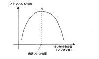
図29の(a)および(c)のようにレンズシフトによるタンジェンシャル位相差がある場合、トラッキング制御によって収束レンズをシフトさせると、位相差トラッキングエラー信号の対称性が悪化し、オフセットが発生する。このDPDTEのオフセットと、レンズシフトとの関係を図30に示す。図30において、横軸は収束レンズの位置を示し、縦軸はDPDTEのオフセット値を示す。
【0010】
図30に示すように、収束レンズの位置とDPDTEのオフセット値とは、レンズ位置が最適なレンズ位置付近において線形性の関係を示す。このDPDTEのオフセットを検出し、DPDTEのオフセットが0となるようにトラッキング駆動値にオフセットを印加することによって、収束レンズ22の位置を移動させ、レンズシフトを補正することができる。
【0011】
次に図28を参照して、レンズシフトを補正する手順を説明する。信号生成回路30の位相差調整回路31a、31bの調整をずらし、タンジェンシャル位相差が発生している状態にする。レンズシフトが発生している場合には、DPDTEのオフセットが発生するので、オフセット測定部61でDPDTEのオフセットを測定する。
【0012】
レンズシフト補正部62はトラッキング制御部の出力値にこのオフセットを印加する。駆動回路91はこのオフセットが印加されたトラッキング制御部の出力値に基づいて収束レンズ22を移動させる。ここで、図30に示す線形性の関係を利用して、オフセット測定部61で検出したDPDTEのオフセットがゼロとなるように収束レンズ22を移動させれば、レンズシフトをゼロにすることができる。
【0013】
【特許文献1】
特開2000−315327号公報
【0014】
【発明が解決しようとする課題】
例えばDVD−RAMディスクのように、トラックに対して内周および外周にそれぞれ1/2トラック分シフトして配置されたアドレスを再生する場合、偏心あるいは光軸倒れ等によってレンズシフトが発生しているとアドレス部におけるRF信号のバランスがくずれる。このため、アドレス部を検出および分離するためのゲート信号が生成できなかったり、アドレス部のRF信号振幅が小さくなることにより、SN比が悪くなり、アドレス情報が正しく再生できないという問題が生じる。
【0015】
これを上述の従来の光ディスク装置におけるレンズシフトの補正方法で解決するためには、図28の信号生成回路で示すようなタンジェンシャル位相差の調整機構(検出器)及び調整回路が必要となる。こため、光ディスク装置のコストダウンをはかったり、光ピックアップを小型化するのが困難になるという課題が生じる。
【0016】
本発明は上記課題に鑑みてなされたものであり、位相差トラッキングエラー信号を使用せず、位相差調整回路が無いような装置や、単純な分割の光検出器を有するような光ピックアップであっても、レンズシフトをゼロにすることのできるトラッキング制御装置および光ディスク装置を提供することを目的とする。
【0017】
【課題を解決するための手段】
本発明のトラッキング制御装置は、情報トラックに対して、おおよそ1/2トラックずつ内周側および外周側にずらして配置した第1のアドレスおよび第2のアドレスあるいは第1のアドレス部および第2のアドレス部を有する情報担体に対し光学的な記録および/または再生を行うために、前記情報担体に向けて光ビームを収束して照射する収束手段と、前記情報担体から得られる前記光ビームの反射光を検出する光検出手段と、前記収束手段を情報トラックを横切る方向に移動させる移動手段とを備えた光学ヘッドを制御する。
【0018】
本発明のトラッキング制御装置は、前記光検出手段の出力より前記情報担体に記録されているアドレスを取得するアドレスリード手段と、前記アドレスリード手段が第1のアドレスを取得したことを判定する第1のアドレスリード判定手段と、前記アドレスリード手段が第2のアドレスを取得したことを判定する第2のアドレスリード判定手段と、所定の距離間隔で前記収束手段の位置を前記移動手段により移動させるためのオフセット設定値を逐次生成し、前記収束手段が移動したそれぞれの位置において、前記第1のアドレスリード判定手段と前記第2のアドレスリード判定手段との判定結果が共にアドレス取得したとする取得回数をカウントするレンズ位置特性測定手段と、前記取得回数の最大値を探索し、前記取得回数が最大値となるときのオフセット設定値に基づいて、前記移動手段により前記収束手段を移動させるレンズシフト調整手段とを備える。
【0019】
また、本発明のトラッキング制御装置は、前記光検出手段が分割し検出した各検出信号の差信号を生成する差信号生成手段と、前記差信号生成手段の出力を所定の第1のレベルと比較しゲートを生成する第1のゲート生成手段と、前記差信号生成手段の出力を所定の第2のレベルと比較しゲートを生成する第2のゲート生成手段と、所定の距離間隔で前記収束手段の位置を前記移動手段により移動させるためのオフセット設定値を逐次生成し、前記収束手段が移動したそれぞれ位置において、前記第1のゲート生成手段が生成するゲートの数および前記第2のゲート生成手段が生成するゲートの数に基づく計測数を求めるレンズ位置特性測定手段と、前記収束手段の前記光検出手段に対する位置ずれが最小なるときの前記計測数を探索し、探索した計測数に対応するオフセット設定値に基づいて、前記移動手段により前記収束手段を移動させるレンズシフト調整手段とを備える。
【0020】
ある好ましい実施形態において、前記計測数は、前記第1のゲート生成手段が生成するゲートの数および前記第2のゲート生成手段が生成するゲートの数の和であって、前記収束手段の前記光検出手段に対する位置ずれが最小なるときの前記計測数はその最大値である。
【0021】
ある好ましい実施形態において、 前記計測数は、前記第1のゲート生成手段が生成するゲートの数および前記第2のゲート生成手段が生成するゲートの数の差であって、前記収束手段の前記光検出手段に対する位置ずれが最小なるときの前記計測数はゼロまたはゼロに最も近い値である。
【0022】
また、本発明のトラッキング制御装置は、前記光検出手段が分割し検出した各検出信号の差信号を生成する差信号生成手段と、前記差信号生成手段の出力の最大を検出するピーク検出手段と、前記差信号生成手段の出力の最小を検出するボトム検出手段と、所定の距離間隔で前記収束手段の位置を前記移動手段により移動させるためのオフセット設定値を逐次生成し、前記収束手段が移動したそれぞれ位置において、前記ピーク検出手段の検出値および前記ボトム検出手段の検出値に基づく計算値を求めるレンズ位置特性測定手段と、前記収束手段の前記光検出手段に対する位置ずれが最小なるときの前記計算値を探索し、探索した計算値に対応するオフセット設定値に基づいて、前記移動手段により前記収束手段を移動させるレンズシフト調整手段とを備える。
【0023】
ある好ましい実施形態において、前記ピーク検出手段の検出値および前記ボトム検出手段の検出値をそれぞれTEmaxおよびTEminと表したとき、前記計算値は、(TEmax+TEmin)/(TEmax−TEmin)であり、前記収束手段の前記光検出手段に対する位置ずれが最小なるときの前記計算値はゼロまたはゼロに最も近い値である。
【0024】
また、本発明のトラッキング制御装置は、前記光検出手段が分割し検出した各検出信号の差信号を生成する差信号生成手段と、前記差信号生成手段の出力より、前記第1のアドレス部の振幅を検出する第1のアドレス振幅検出手段と、前記差信号生成手段の出力より、前記第2のアドレス部の振幅を検出する第2のアドレス振幅検出手段と、所定の距離間隔で前記収束手段の位置を前記移動手段により移動させるためのオフセット設定値を逐次生成し、前記収束手段が移動したそれぞれの位置において、前記第1のアドレス振幅検出手段の出力と前記第2のアドレス振幅検出手段の出力との出力差を求めるレンズ位置特性測定手段と、前記出力差がゼロまたはゼロに最も近い値を探索し、前記出力差がゼロまたはゼロに最も近い値最大値となるときのオフセット設定値に基づいて、前記移動手段により前記収束手段を移動させるレンズシフト調整手段とを備える。
【0025】
また、本発明のトラッキング制御装置は、光ビームを照射したときの反射特性が異なる第1および第2の領域を有する情報担体に対し光学的な記録および/または再生を行うために、前記情報担体に向けて光ビームを収束して照射する収束手段と、前記情報担体から得られる前記光ビームの反射光を分割して検出する光検出手段と、前記収束手段を情報トラックを横切る方向に移動させる移動手段とを備えた光学ヘッドを制御する。トラッキング制御装置は、前記光検出手段が分割し検出した各検出信号の差信号を生成する差信号生成手段と、前記差信号の所定の期間における平均値を測定するオフセット測定手段と、所定の距離間隔で前記収束手段の位置を前記移動手段により移動させるためのオフセット設定値を逐次生成し、前記収束手段が移動したそれぞれの位置における前記平均値を前記情報担体の第1の領域および第2の領域について求めるレンズ位置特性測定手段と、前記情報担体の第1の領域において得られた前記オフセット設定値と前記平均値との関係および第2の領域において得られた前記オフセット設定値と前記平均値との関係から前記収束手段の前記光検出手段に対する位置ずれが最小なるときの前記平均値を探索し、探索した平均値に対応するオフセット設定値に基づいて、前記移動手段により前記収束手段を移動させるレンズシフト調整手段とを備える。
【0026】
ある好ましい実施形態において、前記レンズ位置特性測定手段は、前記取得回数、前記計測数、前記計算値、前記出力差または前記平均値を、前記情報担体を1回転あるいはその整数倍回転させる間取得する。
【0027】
ある好ましい実施形態において、トラッキング制御装置は、前記光検出手段の出力よりトラックずれを検出するトラッキングエラー信号生成手段と、前記トラッキングエラー信号生成手段のオフセットを調整するオフセット調整手段とを更に備え、前記オフセット調整手段によるオフセット調整を行った後に前記レンズ位置特性測定手段を動作させる。
【0028】
ある好ましい実施形態において、トラッキング制御装置は、前記光検出手段の出力よりトラックずれを検出するトラッキングエラー信号生成手段と、前記トラッキングエラー信号生成手段のオフセットを調整するオフセット調整手段とを更に備え、前記オフセット調整手段によるオフセット調整を行う前に前記レンズ位置特性測定手段を動作させる。
【0029】
ある好ましい実施形態において、トラッキング制御装置は、前記光検出手段の出力よりトラックずれを検出するトラッキングエラー信号生成手段と、前記トラッキングエラー信号生成手段のオフセットを調整するオフセット調整手段とを更に備え、前記移動手段による前記収束手段の移動量に応じて前記オフセット調整手段を動作させる。
【0030】
ある好ましい実施形態において、前記情報担体は、凸部および凹部によって形成される情報トラックを含み、前記レンズ位置特性測定手段は、前記情報トラックの凸部および凹部のそれぞれに対して測定を行い、測定結果に基づいて前記レンズシフト調整手段が前記凸部および凹部に対してそれぞれ前記収束手段を移動させる。
【0031】
ある好ましい実施形態において、情報担体の位置に応じて前記レンズ位置特性測定手段およびレンズシフト調整手段を動作させる。
【0032】
ある好ましい実施形態において、前記レンズシフト調整手段は、前記取得回数、前記計測数、前記計算値、前記出力差または前記平均値と前記オフセット設定値との関係から近似関数を決定する近似関数決定手段を含み、前記近似関数から前記収束手段の前記光検出手段に対する位置ずれが最小なるときの前記オフセット設定値を求める。
【0033】
ある好ましい実施形態において、前記レンズシフト調整手段は、前記取得回数、前記計測数、前記計算値、前記出力差または前記平均値がおおよそ一定となる範囲を求め、前記一定となる範囲の中心に対応するオフセット設定値を前記光検出手段に対する位置ずれが最小なるときの前記オフセット設定値とする。
【0034】
ある好ましい実施形態において、前記レンズ位置特性測定手段は、前記情報担体の回転位相に応じて前記取得回数、前記計測数、前記計算値、前記出力差または前記平均値を求める。
【0035】
ある好ましい実施形態において、前記レンズシフト調整手段は、前記情報担体の回転位相に応じて前記オフセット設定値を決定する。
【0036】
ある好ましい実施形態において、トラッキング制御装置は、前記第1のゲート生成手段および前記第2のゲート生成手段は、前記第1のレベルおよび第2のレベルと異なるレベルを用いてアドレスを検出する。
【0037】
ある好ましい実施形態において、前記第1のアドレス振幅検出手段および前記第2のアドレス振幅検出手段は、前記情報担体の第1のアドレス部および第2のアドレス部において振幅がおおよそ一定となる所定の部位で振幅の検出を行う。
【0038】
ある好ましい実施形態において、前記レンズシフト調整手段は、前記情報担体の第1の領域において得られた前記オフセット設定値と前記平均値との関係を示す第1の関数および第2の領域において得られた前記オフセット設定値と前記平均値との関係を示す第2の関数を求め、前記第1の関数および第2の関数の交点から求めることのできるオフセット設定値に基づいて前記移動手段により前記収束手段を移動させる。
【0039】
本発明の光ディスク装置は、情報担体に向けて光ビームを収束して照射する収束手段と、前記情報担体から得られる前記光ビームの反射光を検出する光検出手段と、前記収束手段を情報トラックを横切る方向に移動させる移動手段とを備えた光学ヘッドと、上記いずれかに規定されるトラッキング制御装置を備える。
【0040】
本発明のトラッキング制御方法は、情報トラックに対して、おおよそ1/2トラックずつ内周側および外周側にずらして配置した第1のアドレスおよび第2のアドレスまたは第1のアドレス部および第2のアドレス部を有する情報担体に対し光学的な記録および/または再生を行うために、前記情報担体に向けて光ビームを収束して照射する収束手段と、前記情報担体から得られる前記光ビームの反射光を検出する光検出手段と、前記収束手段を情報トラックを横切る方向に移動させる移動手段とを備えた光学ヘッドを制御する。
【0041】
トラッキング制御方法は、所定の距離間隔で前記収束手段の位置を前記移動手段により移動させるためのオフセット設定値を逐次生成し、前記収束手段が移動したそれぞれの位置において、前記光検出手段の出力より前記情報担体に記録されている前記第1のアドレスおよび前記第2のアドレスを取得した取得回数をカウントするステップと、前記取得回数の最大値を探索し、前記取得回数が最大値となるときのオフセット設定値に基づいて、前記移動手段により前記収束手段を移動させるステップとを包含する。
【0042】
また、本発明のトラッキング制御方法は、前記光検出手段が分割して検出した各検出信号の差信号を生成するステップと、前記差信号と第1および第2のレベルと比較し、前記第1および第2のレベルより前記差信号が大きいとき、第1および第2のゲートを生成するステップと、所定の距離間隔で前記収束手段の位置を前記移動手段により移動させるためのオフセット設定値を逐次生成し、前記収束手段が移動したそれぞれ位置において、生成した前記第1および第2のゲートの数に基づく計測数を求めるステップと、前記収束手段の前記光検出手段に対する位置ずれが最小なるときの前記計測数を探索し、探索した計測数に対応するオフセット設定値に基づいて、前記移動手段により前記収束手段を移動させるステップとを包含する。
【0043】
ある好ましい実施形態において、前記計測数は、前記第1および第2のゲートの数の和であって、前記移動ステップにおける前記収束手段の前記光検出手段に対する位置ずれが最小なるときの計測数はその最大値である。
【0044】
ある好ましい実施形態において、前記計測数は、前記第1および第2のゲートの数の差であって、前記収束手段の前記光検出手段に対する位置ずれが最小なるときの前記計測数はゼロまたはゼロに最も近い値である。
【0045】
また、本発明のトラッキング制御方法は、前記光検出手段が分割して検出した各検出信号の差信号を生成するステップと、前記差信号の最大値および最小値を検出するステップと、所定の距離間隔で前記収束手段の位置を前記移動手段により移動させるためのオフセット設定値を逐次生成し、前記収束手段が移動したそれぞれ位置において、前記最大値および最小値に基づく計算値を求めるステップと、前記収束手段の前記光検出手段に対する位置ずれが最小なるときの前記計算値を探索し、探索した計算値に対応するオフセット設定値に基づいて、前記移動手段により前記収束手段を移動させるステップとを包含する。
【0046】
ある好ましい実施形態において、前記最大値および最小値をそれぞれTEmaxおよびTEminと表したとき、前記計算値は、(TEmax+TEmin)/(TEmax−TEmin)であり、前記収束手段の前記光検出手段に対する位置ずれが最小なるときの前記計算値はゼロまたはゼロに最も近い値である。
【0047】
また、本発明のトラッキング制御方法は、前記光検出手段が分割して検出した各検出信号の差信号を生成するステップと、前記差信号の前記第1のアドレス部および第2のアドレス部における振幅を検出するステップと、所定の距離間隔で前記収束手段の位置を前記移動手段により移動させるためのオフセット設定値を逐次生成し、前記収束手段が移動したそれぞれの位置において、前記差信号の第1のアドレス部における振幅と、第2のアドレス部における振幅との振幅差を求めるステップと、前記振幅差がゼロまたはゼロに最も近い値を探索し、前記振幅差がゼロまたはゼロに最も近い値となるときのオフセット設定値に基づいて、前記移動手段により前記収束手段を移動させるステップとを包含する。
【0048】
また、本発明のトラッキング制御方法は、光ビームを照射したときの反射特性が異なる第1および第2の領域を有する情報担体に対し光学的な記録および/または再生を行うために、前記情報担体に向けて光ビームを収束して照射する収束手段と、前記情報担体から得られる前記光ビームの反射光を分割して検出する光検出手段と、前記収束手段を情報トラックを横切る方向に移動させる移動手段とを備えた光学ヘッドを制御する。トラッキング制御装置は、前記光検出手段が分割して検出した各検出信号の差信号を生成するステップと、前記差信号の所定の期間における平均値を測定するステップと、所定の距離間隔で前記収束手段の位置を前記移動手段により移動させるためのオフセット設定値を逐次生成し、前記収束手段が移動したそれぞれの位置における前記平均値を前記情報担体の第1の領域および第2の領域について求めるステップと、前記情報担体の第1の領域において得られた前記オフセット設定値と前記平均値との関係、および、前記第2の領域において得られた前記オフセット設定値と前記平均値との関係およびから、前記収束手段の前記光検出手段に対する位置ずれが最小なるときの前記平均値を探索し、探索した平均値に対応するオフセット設定値に基づいて、前記移動手段により前記収束手段を移動させるステップとを包含する。
【0049】
ある好ましい実施形態において、前記情報担体の第1の領域において得られた前記オフセット設定値と前記平均値との関係を示す第1の関数および第2の領域において得られた前記オフセット設定値と前記平均値との関係を示す第2の関数を求め、前記第1の関数および第2の関数の交点から求めることのできるオフセット設定値に基づいて前記移動手段により前記収束手段を移動させる。
【0050】
上記いずれかに記載のトラッキング制御方法に規定されている各ステップコンピュータに実行させるためのプログラムは、コンピュータ読み取り可能な記録媒体に記録されている。
【0051】
【発明の実施の形態】
(第1の実施形態)
図1は本実施形態によるトラッキング制御装置およびこのトラッキング制御装置を用いた光ディスク装置の構成を示すブロック図である。光ディスク装置11において、光ピックアップ120は、レーザ等の発光素子(不図示)、収束手段である収束レンズ22、および移動手段であるアクチュエータ23を有しており、収束レンズ22は光ビーム21を情報担体である光ディスク110に向けて収束しながら照射する。光ディスク110は例えば情報トラックに対して約1/2トラックずらして配置されており、アドレス情報を含むアドレス部を有する。アクチュエータ23は情報トラックを横切るように収束レンズ22を移動させる。
【0052】
光ピックアップ120はさらに光ディスクの直径方向に分割された検出部AおよびBを含む光検出器124を有しており、光ディスク110の情報記録面において反射した光ビーム21’を光検出手段である光検出器124で検出する。光検出器124の検出部AおよびBの出力は、減算回路130に入力され、検出部Aで検出した光量に相当する信号Aから検出部Bで検出した光量に相当する信号Bを減じた信号、つまり、(A−B)のRF差信号を生成する。RF差信号はローパスフィルタ(LPF)131を通過し、トラッキングエラー信号(以下TEと称す)としてトラッキング制御装置であるデジタルシグナルプロセッサ(DSP)150に入力される。
【0053】
DSP150は、信号処理部140、レンズ位置特性測定部162、メモリ163、最適レンズ位置探索部164、レンズ位置設定部161、A/D変換器51、オフセット調整部52、トラッキング制御部53およびD/A変換器54を含む。
【0054】
A/D変換器51はTEをデジタル信号に変換する。オフセット調整部52はデジタル信号に変換されたTEにトラッキング制御における所定のオフセットを加算し、トラッキング制御部53へ出力する。トラッキング制御部53は、位相補償および低域補償を行うフィルタ演算をデジタル信号に変換されたTEに施すことによってトラッキング駆動値を生成する。生成されたトラッキング駆動値は、レンズ位置設定部161の出力と加算され、D/A変換器54により再びアナログ信号に変換される。D/A変換器54の出力は、トラッキング駆動信号となり、駆動回路91へ出力される。
【0055】
駆動回路91はトラッキング駆動信号を電流増幅して光ピックアップ120に内蔵された移動手段であるアクチュエータ23を駆動し、トラッキング制御を行う。この時、DSP150のレンズ位置設定部161はトラッキング制御部53の出力であるトラッキング駆動値に対してオフセットを加算し、収束レンズ22の光検出器124に対する位置をずらすことができる。
【0056】
また、減算回路130からRF差信号がDSP150の信号処理部140へ入力される。この信号処理部140によりアドレス情報を得ることができる。図2は信号処理部140の詳細な構成を示すブロック図である。信号処理部140において、ハイパスフィルタ(HPF)141はRF差信号の直流成分を除去する。直流成分が除去されたRF差信号は、2値化回路142によって、適当なスライスレベルで2値化したデータに変換される。2値化されたデータ信号はPLL回路143に入力され、2値化されたデータ信号に基づいて、データ抽出のための同期クロック信号が周波数および位相制御される。PLL回路143の出力はアドレスリード手段であるデコーダ144へ入力され、デコーダ144は再生情報、即ちトラックあるいはセクタアドレスのコードデータを出力する。
【0057】
第1のアドレスリード判定手段および第2のアドレスリード判定手段であるアドレスリード判定部145は、デコーダ144の出力結果に基づき、正しくアドレスがリードできたか否かを判定する。アドレスがリードできたと判定した場合には、図1に示すように、レンズ位置特性測定部162にアドレスがリードできたことを示すアドレスOK信号を出力する。
【0058】
レンズ位置特性測定手段であるレンズ位置特性測定部162は、所定の距離間隔で収束レンズ22の位置を移動させるためのオフセットをレンズ位置設定部161が逐次発生するよう、レンズ位置設定部161にオフセット設定値を出力するとともに、そのオフセット設定値において受け取るアドレスOK信号の数をカウントする。所定の距離間隔は必ずしも等間隔でなくてもよい。そして、オフセット設定値およびそのときのアドレスOK信号の数をメモリ163に出力する。メモリ163はオフセット設定値およびアドレスOK信号の数を逐次記憶する。レンズ位置設定部161は、レンズ位置特性測定部162から受け取るオフセット設定値に基づいて、逐次オフセットを発生し、オフセットをトラッキング制御部53の出力であるトラッキング駆動値に加える。
【0059】
レンズシフト調整手段である最適レンズ位置探索部164は以下において詳述するように、アドレスOK信号の数の最大値を求め、そのときのオフセット設定値を最適レンズ位置を与えるオフセット設定値として、レンズ位置設定部161に出力する。レンズ位置設定部161は、最適レンズ位置を与えるオフセット設定値に基づいて、オフセットを生成し、トラッキング駆動値に加える。これにより、レンズシフトをゼロに設定できる。
【0060】
図3は情報担体である光ディスク110の物理的な構造を説明するための模式図である。光ディスク110において、たとえば、情報記録面に対して凸部によって形成されるトラックT1と凹部によって形成されるトラックT2とが交互に配置されている。トラックT1およびT2には、濃淡のマーク等によってユーザデータなどの情報が記録される。第1のアドレス部A1は、トラックT1に対して、ディスクの内周側にトラックの約1/2本分シフトした位置に記録され、第2のアドレス部A2は、トラックT1に対して、ディスクの外周側にトラックの約1/2本シフトした位置に記録されている。
【0061】
図4は図3に示した光ディスク110のアドレス部を再生した場合のRF差信号の出力波形の一例である。図4の(a)はレンズシフトがない場合、(b)は内周側にレンズシフトしている場合の波形である。図4(b)のように内周側にレンズシフトしている場合には、2つのアドレス部の波形が非対称となり、外周側のアドレス部は十分なRF信号振幅を得られず、アドレスを再生できなくなる。
【0062】
図2に示すアドレスリード判定部145は、第1のアドレス部A1および第2のアドレス部A2の両方の再生でエラーがない場合にアドレスがリードできたと判定して、アドレスOK信号を生成し、レンズ位置特性測定部162へ出力する。図4から明らかなように、レンズシフトが発生している場合には、アドレスOK信号の出力される頻度が低くなる。したがって、レンズ位置特性測定部162がカウントするアドレスOK信号の数は、レンズシフトが大きい場合よりもレンズシフトが小さい場合の方が大きくなることを利用してレンズシフトを検出することができる。
【0063】
レンズ位置特性測定部162が設定したオフセット設定値にとアドレスOK信号の数との関係を図5に示す。図5において、横軸はオフセット設定値を示し、縦軸はアドレスOK信号の数を示す。オフセット設定値に基づき、レンズ位置設定部161がオフセットを発生し、トラッキング駆動値に加算されるので、横軸は相対的なレンズ位置も示していることになる。図5に示す特性において、アドレスOK信号が最大となる点Aはレンズシフトがない最適レンズ位置である。最適レンズ位置探索部164はメモリ163に保存されたアドレスOK信号の数の最大値を求め、そのときのオフセット設定値を最適レンズ位置としてレンズ位置設定部161に出力する。レンズ位置設定部161は、受け取ったオフセット設定値に基づいてオフセットを生成し、トラッキング駆動値にオフセットを重畳する。オフセットが加算されたトラッキング駆動信号が駆動回路91から出力され、これにより、レンズシフトが補正され、アドレス部におけるRF差信号は、常に図4(a)に示すような対称性のよい良好な波形となる。つまり、良好なトラッキング信号、RF信号を得ることができ、信頼性の高い光ディスク装置を提供することが可能となる。
【0064】
なお本実施形態において、光検出器124は2分割された検出領域を備えていた。しかし、例えば従来例の図28に示したような4分割の光検出器24を用い、検出部Aおよび検出部Cの出力を加算した信号、ならびに、検出部Bおよび検出部Dの出力を加算した信号を用いて処理を行うことによって、同様の効果が得られる。
【0065】
上述したように本発明によれば、情報担体に設けられた第1のアドレスおよび第2のアドレスを再生したときに得られる信号をもとに、光検出器に対する収束レンズのレンズシフトを補正する。特に、本実施形態では、第1のアドレスおよび第2のアドレスは、情報トラックに対して、おおよそ1/2トラックずつ内周側および外周側にずらして配置されているので、両方のアドレスが正しく再生できているとき、レンズシフトがゼロまたは小さい値になることを利用する。
【0066】
具体的には、収束レンズの位置を変化させためオフセット設定値を逐次発生させ、光検出器に対する収束レンズの位置を変化させる。そして、それぞれの位置において、第1のアドレスおよび第2のアドレスが正しく再生できた回数を求める。その回数が最も多くなるときのオフセット設定値を用いて、収束レンズを移動させれば、レンズシフトをゼロまたは最小となるよう補正することができる。
【0067】
これにより、位相差トラッキングエラー信号を使用しない、位相差調整回路が無いような装置や、単純な分割の光検出器を有するような光ピックアップにおいて、光学部品の取り付け誤差や垂直設置に伴う初期の対物レンズ移動による光軸倒れが発生しても、良好なトラッキング信号およびRF信号を得ることができる。
【0068】
(第2の実施形態)
図6は本実施形態によるトラッキング制御装置およびこのトラッキング制御装置を用いた光ディスク装置の構成を示すブロック図である。光ディスク装置12において、第1の実施形態の光ディスク装置11と同じ構成要素には同じ参照符号を付している。
【0069】
光ピックアップ120は、レーザ等の発光素子(不図示)、収束手段である収束レンズ22、および移動手段であるアクチュエータ23を有しており、収束レンズ22は光ビーム21を情報担体である光ディスク110に向けて収束しながら照射する。
【0070】
光ピックアップ120はさらに光ディスクの直径方向に分割された検出部AおよびBを含む光検出器124を有しており、光ディスク110の情報記録面において反射した光ビーム21’を光検出手段である光検出器124で検出する。光検出器124の検出部AおよびBの出力は、減算回路130に入力され、検出部Aで検出した光量に相当する信号Aから検出部Bで検出した光量に相当する信号Bを減じた信号、つまり、(A−B)のRF差信号を生成する。RF差信号はローパスフィルタ(LPF)131を通過し、トラッキングエラー信号(以下TEと称す)としてトラッキング制御装置であるデジタルシグナルプロセッサ(DSP)250に入力される。
【0071】
DSP250は、アドレスゲート部240、レンズ位置特性測定部262、メモリ163、最適レンズ位置探索部264、レンズ位置設定部161、A/D変換器51、オフセット調整部52、トラッキング制御部53およびD/A変換器54を含む。
【0072】
A/D変換器51はTEをデジタル信号に変換する。オフセット調整部52はデジタル信号に変換されたTEに所定のオフセットを加算し、トラッキング制御部53へ出力する。トラッキング制御部53は、たとえば、位相補償および低域補償を行うフィルタ演算をデジタル信号に変換されたTEに施すことによってトラッキング駆動値を生成する。生成されたトラッキング駆動値は、レンズ位置設定部161の出力と加算され、D/A変換器54により再びアナログ信号に変換される。D/A変換器54の出力は、トラッキング駆動信号となり、駆動回路91へ出力される。
【0073】
駆動回路91はトラッキング駆動信号を電流増幅して光ピックアップ120に内蔵された移動手段であるアクチュエータ23を駆動し、トラッキング制御を行う。この時、DSP250のレンズ位置設定部161はトラッキング制御部53の出力であるトラッキング駆動値に対してオフセットを加算し、収束レンズ22の光検出器124に対する位置をずらすことができる。
【0074】
また、LPF131からの出力であるTEは、アドレスゲート部240へ入力される。アドレスゲート部240は、TEに基づいてゲート信号を生成しその数をカウントする。
【0075】
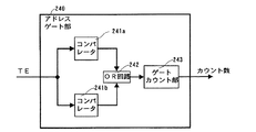
図7はアドレスゲート部240のより具体的な構成を示すブロック図である。アドレスゲート部240は、第1のゲート生成手段であるコンパレータ241aおよび第2のゲート生成手段であるコンパレータ241bを備える。コンパレータ241a、241bは、TEが所定のレベルを超えた場合に、出力信号をそれぞれOR回路242へ出力する。OR回路242は、コンパレータ241aまたはコンパレータ241bから信号を受け取ったとき出力信号を生成する。カウント手段であるゲートカウント部243はOR回路242の出力回数をカウントし、カウント数をレンズ位置特性測定手段であるレンズ位置特性測定部262に出力する。
【0076】
レンズ位置特性測定部262は、所定の時間間隔および所定の距離間隔で収束レンズ22の位置を移動させるためのオフセットをレンズ位置設定部161が逐次発生するよう、レンズ位置設定部161にオフセット設定値を出力するとともに、そのオフセット設定値においてアドレスゲート部240から受け取るカウント数を数える。所定の距離間隔は必ずしも等間隔でなくてもよい。そして、オフセット設定値およびそのときのカウント数をメモリ163に出力する。メモリ163はオフセット設定値およびカウント数を逐次記憶する。レンズ位置設定部261は、レンズ位置特性測定部162から受け取るオフセット設定値に基づいて、逐次オフセットを発生し、オフセットをトラッキング制御部53の出力であるトラッキング駆動値に加える。
【0077】
レンズシフト調整手段である最適レンズ位置探索部264は以下において詳述するように、カウント数の最大値を求め、そのときのオフセット設定値を最適レンズ位置を与えるオフセット設定値として、レンズ位置設定部161に出力する。レンズ位置設定部161は、最適レンズ位置を与えるオフセット設定値に基づいて、オフセットを生成し、トラッキング駆動値に加える。これにより、レンズシフトをゼロに設定できる。
【0078】
図8(a)および(b)は、アドレスゲート部240における各部の信号の波形を示している。図8(a)に示すように、アドレスゲート部240にレンズシフトがない場合のTEが入力されると、コンパレータ241a、241bに設定されたコンパレータレベルa、bをTEのアドレス部が超えるため、コンパレータ241a、241bからそれぞれ外周ゲート信号および内周ゲート信号が出力される。この場合、OR回路242は、外周ゲート信号および内周ゲート信号を数え、カウント数2を出力する。
【0079】
一方、図8(b)に示すように、内周側にレンズシフトが生じた場合のTEが入力される場合、コンパレータ241aのaをTEのアドレス部は超えない。このため、外周ゲート信号は生成されず、内周ゲート信号のみが、コンパレータ241bから生成される。この場合には、OR回路242は、カウント数1を出力する。
【0080】
図8では1つのアドレス部しか示していないが、レンズ位置特性測定部262は、あるオフセット設定値において複数のアドレス部を受け取るように、オフセット設定値を発生させる時間間隔を設定する。したがって、レンズシフトが生じている場合には、生成したゲート信号のカウント数も小さくなる。
【0081】
レンズ位置特性測定部262が設定したオフセット設定値に基づくレンズの位置と生成したゲートのカウント数との関係を図9に示す。図9において、横軸は収束レンズの位置を示し、縦軸はゲートのカウント数を示す。オフセット設定値に基づき、レンズ位置設定部161がオフセットを発生し、トラッキング駆動値に加算されるので、横軸は相対的なレンズ位置も示していることになる。図9に示す特性において、カウント数が最大となる点Aはレンズシフトがない最適レンズ位置である。最適レンズ位置探索部264はメモリ163に保存されたカウント数の最大値を求め、そのときのオフセット設定値を最適レンズ位置としてレンズ位置設定部161に出力する。レンズ位置設定部161は、受け取ったオフセット設定値に基づいてオフセットを生成し、トラッキング駆動値にオフセットを重畳する。オフセットが加算されたトラッキング駆動信号が駆動回路91から出力され、これにより、レンズシフトが補正され、アドレス部におけるRF差信号は、常に図4(a)に示すような対称性のよい良好な波形となる。つまり、良好なトラッキング信号、RF信号を得ることができ、信頼性の高い光ディスク装置を提供することが可能となる。
【0082】
上述したように本発明によれば、情報担体に設けられた第1のアドレスおよび第2のアドレスを再生したときに得られる信号をもとに、光検出器に対する収束レンズのレンズシフトを補正する。特に、本実施形態では、光ディスクの直径方向に分割して検出した各信号の差信号を、第1および第2のレベルと比較し、それぞれのレベルを差信号が超えた回数をカウントする。第1のアドレスおよび第2のアドレスは、情報トラックに対して、おおよそ1/2トラックずつ内周側および外周側にずらして配置されているので、第1のレベルを超えた回数と第2のレベルを超えたときの回数との和が最大となるとき、レンズシフトがゼロまたは小さい値になることを利用する。
【0083】
具体的には、収束レンズの位置を変化させためオフセット設定値を逐次発生させ、光検出器に対する収束レンズの位置を変化させる。そして、それぞれの位置において、第1のレベルを超えた回数と第2のレベルを超えたときの回数との和を求める。その回数が最も多くなるときのオフセット設定値を用いて、収束レンズを移動させれば、レンズシフトをゼロまたは最小となるよう補正することができる。
【0084】
これにより、位相差トラッキングエラー信号を使用しない、位相差調整回路が無いような装置や、単純な分割の光検出器を有するような光ピックアップにおいて、光学部品の取り付け誤差や垂直設置に伴う初期の対物レンズ移動による光軸倒れが発生しても、良好なトラッキング信号およびRF信号を得ることができる。
【0085】
(第3の実施形態)
図10は本実施形態によるトラッキング制御装置およびこのトラッキング制御装置を用いた光ディスク装置の構成を示すブロック図である。光ディスク装置13において、第1の実施形態の光ディスク装置11と同じ構成要素には同じ参照符号を付している。
【0086】
光ピックアップ120は、レーザ等の発光素子(不図示)、収束手段である収束レンズ22、および移動手段であるアクチュエータ23を有しており、収束レンズ22は光ビーム21を情報担体である光ディスク110に向けて収束しながら照射する。
【0087】
光ピックアップ120はさらに光ディスクの直径方向に分割された検出部AおよびBを含む光検出器124を有しており、光ディスク110の情報記録面において反射した光ビーム21’を光検出手段である光検出器124で検出する。光検出器124の検出部AおよびBの出力は、減算回路130に入力され、検出部Aで検出した光量に相当する信号Aから検出部Bで検出した光量に相当する信号Bを減じた信号、つまり、(A−B)のRF差信号を生成する。RF差信号はローパスフィルタ(LPF)131を通過し、トラッキングエラー信号(以下TEと称す)としてトラッキング制御装置であるデジタルシグナルプロセッサ(DSP)350に入力される。
【0088】
DSP350は、アドレスゲート部340、レンズ位置特性測定部362、メモリ163、最適レンズ位置探索部364、レンズ位置設定部161、A/D変換器51、オフセット調整部52、トラッキング制御部53およびD/A変換器54を含む。
【0089】
A/D変換器51はTEをデジタル信号に変換する。オフセット調整部52はデジタル信号に変換されたTEに所定のオフセットを加算し、トラッキング制御部53へ出力する。トラッキング制御部53は、たとえば、位相補償および低域補償を行うフィルタ演算をデジタル信号に変換されたTEに施すことによってトラッキング駆動値を生成する。生成されたトラッキング駆動値は、レンズ位置設定部161の出力と加算され、D/A変換器54により再びアナログ信号に変換される。D/A変換器54の出力は、トラッキング駆動信号となり、駆動回路91へ出力される。
【0090】
駆動回路91はトラッキング駆動信号を電流増幅して光ピックアップ120に内蔵された移動手段であるアクチュエータ23を駆動し、トラッキング制御を行う。この時、DSP350のレンズ位置設定部161はトラッキング制御部53の出力であるトラッキング駆動値に対してオフセットを加算し、収束レンズ22の光検出器124に対する位置をずらすことができる。
【0091】
また、LPF131からの出力であるTEは、アドレスゲート部340へ入力される。アドレスゲート部340は、TEに基づいてゲート信号を生成しその数をカウントする。
【0092】
図11はアドレスゲート部340のより具体的な構成を示すブロック図である。アドレスゲート部340は、第1のゲート生成手段であるコンパレータ341aおよび第2のゲート生成手段であるコンパレータ341bと、カウント手段であるゲートカウント部342a、342bとを備える。
【0093】
コンパレータ341a、341bは、それぞれTEを受け取り、TEが所定のコンパレータレベルを超えたときにゲート信号をゲートカウント部342a、342bを出力する。ゲートカウント部342a、342bはゲート信号の数をカウントし、その数をそれぞれレンズ位置特性測定手段であるレンズ位置特性測定部362へ出力する。
【0094】
レンズ位置特性測定部362は、所定の時間間隔および所定の距離間隔で収束レンズ22の位置を移動させるためのオフセットをレンズ位置設定部161が逐次発生するよう、レンズ位置設定部161にオフセット設定値を出力するとともに、そのオフセット設定値においてアドレスゲート部340のゲートカウント部342a、342bから受け取るカウント数の差を求める。所定の距離間隔は必ずしも等間隔でなくてもよい。そして、オフセット設定値およびそのときのカウント数の差をメモリ163に出力する。メモリ163はオフセット設定値およびカウント数の差を逐次記憶する。レンズ位置設定部161は、レンズ位置特性測定部362から受け取るオフセット設定値に基づいて、逐次オフセットを発生し、オフセットをトラッキング制御部53の出力であるトラッキング駆動値に加える。
【0095】
レンズシフト調整手段である最適レンズ位置探索部364は以下において詳述するように、カウント数の差がゼロまたはゼロに最も近い値となるときのオフセット設定値を最適レンズ位置を与えるオフセット設定値として、レンズ位置設定部161に出力する。レンズ位置設定部161は、最適レンズ位置を与えるオフセット設定値に基づいて、オフセットを生成し、トラッキング駆動値に加える。これにより、レンズシフトをゼロに設定できる。
【0096】
図8(a)に示すように、アドレスゲート部340にレンズシフトがない場合のTEが入力されると、コンパレータ341a、341bに設定されたコンパレータレベルa、bをTEのアドレス部が超えるため、コンパレータ341a、341bからそれぞれ外周ゲート信号および内周ゲート信号が出力される。この場合、ゲートカウント部342a、342bから出力されるゲート信号のカウント数はそれぞれ1となり、カウント数の差はゼロとなる。
【0097】
一方、図8(b)に示すように、内周側にレンズシフトが生じた場合のTEが入力される場合、コンパレータ341aのコンパレータレベルaをTEのアドレス部は超えない。このため、外周ゲート信号は生成されず、内周ゲート信号のみが、コンパレータ341bから生成される。この場合には、ゲートカウント部342a、342bから出力されるゲート信号のカウント数は1およびゼロとなり、カウント数の差は1となる。
【0098】
第2の実施形態と同様、複数のアドレス部をアドレスゲート部340が受け取るように、オフセット設定値を発生させる時間間隔を設定することによって、より正確なカウント数の差とオフセット設定値に基づくレンズの位置との関係が求められる。
【0099】
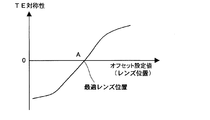
レンズ位置特性測定部362が設定したオフセット設定値に基づくレンズの位置とカウント数の差との関係を図12に示す。図12において、横軸は収束レンズの位置を示し、縦軸はゲートのカウント数の差を示す。オフセット設定値に基づき、レンズ位置設定部161がオフセットを発生し、トラッキング駆動値に加算されるので、横軸は相対的なレンズ位置も示していることになる。図12に示す特性において、カウント数の差がゼロとなる点Aはレンズシフトがない最適レンズ位置である。最適レンズ位置探索部364はメモリ163に保存されたカウント数の差がゼロまたはゼロに最も近い値を探索し、そのときのオフセット設定値を最適レンズ位置としてレンズ位置設定部161に出力する。レンズ位置設定部161は、受け取ったオフセット設定値に基づいてオフセットを生成し、トラッキング駆動値にオフセットを重畳する。オフセットが加算されたトラッキング駆動信号が駆動回路91から出力され、これにより、レンズシフトが補正され、アドレス部におけるRF差信号は、常に図4(a)に示すような対称性のよい良好な波形となる。つまり、良好なトラッキング信号、RF信号を得ることができ、信頼性の高い光ディスク装置を提供することが可能となる。
【0100】
上述したように本発明によれば、情報担体に設けられた第1のアドレスおよび第2のアドレスを再生したときに得られる信号をもとに、光検出器に対する収束レンズのレンズシフトを補正する。特に、本実施形態では、光ディスクの直径方向に分割して検出した各信号の差信号の第1のアドレス部および第2のアドレス部分において、第1および第2のレベルと比較し、それぞれのレベルを差信号が超えた回数をカウントする。第1のアドレスおよび第2のアドレスは、情報トラックに対して、おおよそ1/2トラックずつ内周側および外周側にずらして配置されているので、第1のレベルを超えた回数と第2のレベルを超えたときの回数との差がゼロまたはゼロにもっとも近い値となるとき、レンズシフトがゼロまたは小さい値になることを利用する。
【0101】
具体的には、収束レンズの位置を変化させためオフセット設定値を逐次発生させ、光検出器に対する収束レンズの位置を変化させる。そして、それぞれの位置において、第1のレベルを超えた回数と第2のレベルを超えたときの回数との差を求める。その回数がゼロまたはゼロに最も近い値となるときのオフセット設定値を用いて、収束レンズを移動させれば、レンズシフトをゼロまたは最小となるよう補正することができる。
【0102】
これにより、位相差トラッキングエラー信号を使用しない、位相差調整回路が無いような装置や、単純な分割の光検出器を有するような光ピックアップにおいて、光学部品の取り付け誤差や垂直設置に伴う初期の対物レンズ移動による光軸倒れが発生しても、良好なトラッキング信号およびRF信号を得ることができる。
【0103】
(第4の実施形態)
図13は本実施形態によるトラッキング制御装置およびこのトラッキング制御装置を用いた光ディスク装置の構成を示すブロック図である。光ディスク装置14において、第1の実施形態の光ディスク装置11と同じ構成要素には同じ参照符号を付している。
【0104】
光ピックアップ120は、レーザ等の発光素子(不図示)、収束手段である収束レンズ22、および移動手段であるアクチュエータ23を有しており、収束レンズ22は光ビーム21を情報担体である光ディスク110に向けて収束しながら照射する。
【0105】
光ピックアップ120はさらに光ディスクの直径方向に分割された検出部AおよびBを含む光検出器124を有しており、光ディスク110の情報記録面において反射した光ビーム21’を光検出手段である光検出器124で検出する。光検出器124の検出部AおよびBの出力は、減算回路130に入力され、検出部Aで検出した光量に相当する信号Aから検出部Bで検出した光量に相当する信号Bを減じた信号、つまり、(A−B)のRF差信号を生成する。RF差信号はローパスフィルタ(LPF)131を通過し、トラッキングエラー信号(以下TEと称す)としてトラッキング制御装置であるデジタルシグナルプロセッサ(DSP)450に入力される。
【0106】
DSP450は、対称性検出部440、レンズ位置特性測定部462、メモリ163、最適レンズ位置探索部464、レンズ位置設定部161、A/D変換器51、オフセット調整部52、トラッキング制御部53およびD/A変換器54を含む。
【0107】
A/D変換器51はTEをデジタル信号に変換する。オフセット調整部52はデジタル信号に変換されたTEに所定のオフセットを加算し、トラッキング制御部53へ出力する。トラッキング制御部53は、たとえば、位相補償および低域補償を行うフィルタ演算をデジタル信号に変換されたTEに施すことによってトラッキング駆動値を生成する。生成されたトラッキング駆動値は、レンズ位置設定部161の出力と加算され、D/A変換器54により再びアナログ信号に変換される。D/A変換器54の出力は、トラッキング駆動信号となり、駆動回路91へ出力される。
【0108】
駆動回路91はトラッキング駆動信号を電流増幅して光ピックアップ120に内蔵された移動手段であるアクチュエータ23を駆動し、トラッキング制御を行う。この時、DSP450のレンズ位置設定部161はトラッキング制御部53の出力であるトラッキング駆動値に対してオフセットを加算し、収束レンズ22の光検出器124に対する位置をずらすことができる。
【0109】
また、LPF131からの出力であるTEは、対称性検出部440へ入力される。対称性検出部440は、TEのアドレス部の対称性を検出する。
【0110】
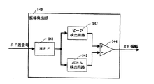
図14は対称性検出部440のより具体的な構成を示すブロック図である。対称性検出部440は、ピーク検出手段であるピーク検出回路441およびボトム検出手段であるボトム検出回路442を含む。ピーク検出回路441は、アドレス部におけるTEの最大値TEmaxをホールドする。また、ボトム検出回路442はアドレス部におけるTEの最小値TEminをホールドする。対称性検出部440は、TEmaxおよびTEminをレンズ位置検出手段であるレンズ位置特性測定部462へ出力する。
【0111】
レンズ位置特性測定部462は、所定の距離間隔で収束レンズ22の位置を移動させるためのオフセットをレンズ位置設定部161が逐次発生するよう、レンズ位置設定部161にオフセット設定値を出力する。所定の距離間隔は必ずしも等間隔でなくてもよい。また、そのオフセット設定値においてTE対称性(TEmax+TEmin)/(TEmax−TEmin)を計算する。そして、オフセット設定値およびそのときのTE対称性をメモリ163に出力する。メモリ163はオフセット設定値およびTE対称性を逐次記憶する。レンズ位置設定部161は、レンズ位置特性測定部462から受け取るオフセット設定値に基づいて、逐次オフセットを発生し、オフセットをトラッキング制御部53の出力であるトラッキング駆動値に加える。
【0112】
レンズシフト調整手段である最適レンズ位置探索部464は以下において詳述するように、TE対称性がゼロまたはゼロに最も近い値となるときのオフセット設定値を最適レンズ位置を与えるオフセット設定値として、レンズ位置設定部161に出力する。レンズ位置設定部161は、最適レンズ位置を与えるオフセット設定値に基づいて、オフセットを生成し、トラッキング駆動値に加える。これにより、レンズシフトをゼロに設定できる。
【0113】
図15(a)および(b)は、アドレスゲート部440に入力されるTEのアドレス部における波形を拡大して模式的に示している。
【0114】
図15(a)に示すように、レンズシフトがない場合のアドレス部におけるTEの波形は、ゼロに対して対称となる。このため、ピーク検出回路441の出力TEmaxとボトム検出回路442の出力TEminとから計算されるTE対称性(TEmax+TEmin)/(TEmax−TEmin)は、ゼロまたはゼロに近い値となる。
【0115】
一方、図15(b)に示すように、内周側にレンズシフトが生じている場合のアドレス部におけるTEの波形はゼロに対して非対称となる。このため、ピーク検出回路441の出力TEmaxとボトム検出回路442の出力TEminとから計算されるTE対称性(TEmax+TEmin)/(TEmax−TEmin)は、負の値となる。
【0116】
レンズ位置特性測定部462が設定したオフセット設定値に基づくレンズの位置とTE対称性との関係を図16に示す。図16において、横軸は収束レンズの位置を示し、縦軸はTE対称性を示す。オフセット設定値に基づき、レンズ位置設定部161がオフセットを発生し、トラッキング駆動値に加算されるので、横軸は相対的なレンズ位置も示していることになる。図16に示す特性において、TE対称性がゼロとなる点Aはレンズシフトがない最適レンズ位置である。最適レンズ位置探索部464はメモリ163に保存されたTE対称性がゼロまたはゼロに最も近い値(たとえば最もゼロに近い値、あるいは、ゼロに近い閾値を設定し、この閾値よりもゼロに近い値など)を探索し、そのときのオフセット設定値を最適レンズ位置としてレンズ位置設定部161に出力する。レンズ位置設定部161は、受け取ったオフセット設定値に基づいてオフセットを生成し、トラッキング駆動値にオフセットを重畳する。オフセットが加算されたトラッキング駆動信号が駆動回路91から出力され、これにより、レンズシフトが補正され、アドレス部におけるRF差信号は、常に図4(a)に示すような対称性のよい良好な波形となる。つまり、良好なトラッキング信号、RF信号を得ることができ、信頼性の高い光ディスク装置を提供することが可能となる。
【0117】
上述したように本発明によれば、情報担体に設けられた第1のアドレスおよび第2のアドレスを再生したときに得られる信号をもとに、光検出器に対する収束レンズのレンズシフトを補正する。特に、本実施形態では、光ディスクの直径方向に分割して検出した各信号の差信号の第1のアドレスおよび第2のアドレスにおける最大値と最小値とを求める。第1のアドレスおよび第2のアドレスは、情報トラックに対して、おおよそ1/2トラックずつ内周側および外周側にずらして配置されているので、(最大値+最小値)/(最大値−最小値)がゼロまたはゼロに最も近い値となるとき、レンズシフトがゼロまたは小さい値になることを利用する。
【0118】
具体的には、収束レンズの位置を変化させためオフセット設定値を逐次発生させ、光検出器に対する収束レンズの位置を変化させる。そして、それぞれの位置において、(最大値+最小値)/(最大値−最小値)を求める。その値がゼロまたはゼロに最も近い値となるときのオフセット設定値を用いて、収束レンズを移動させれば、レンズシフトをゼロまたは最小となるよう補正することができる。
【0119】
これにより、位相差トラッキングエラー信号を使用しない、位相差調整回路が無いような装置や、単純な分割の光検出器を有するような光ピックアップにおいて、光学部品の取り付け誤差や垂直設置に伴う初期の対物レンズ移動による光軸倒れが発生しても、良好なトラッキング信号およびRF信号を得ることができる。
【0120】
(第5の実施形態)
図17は本実施形態によるトラッキング制御装置およびこのトラッキング制御装置を用いた光ディスク装置の構成を示すブロック図である。光ディスク装置15において、第1の実施形態の光ディスク装置11と同じ構成要素には同じ参照符号を付している。
【0121】
光ピックアップ120は、レーザ等の発光素子(不図示)、収束手段である収束レンズ22、および移動手段であるアクチュエータ23を有しており、収束レンズ22は光ビーム21を情報担体である光ディスク110に向けて収束しながら照射する。
【0122】
光ピックアップ120はさらに光ディスクの直径方向に分割された検出部AおよびBを含む光検出器124を有しており、光ディスク110の情報記録面において反射した光ビーム21’を光検出手段である光検出器124で検出する。光検出器124の検出部AおよびBの出力は、減算回路230に入力され、検出部Aで検出した光量に相当する信号Aから検出部Bで検出した光量に相当する信号Bを減じた信号、つまり、(A−B)のRF差信号を生成する。RF差信号はローパスフィルタ(LPF)131を通過し、トラッキングエラー信号(以下TEと称す)としてトラッキング制御装置であるデジタルシグナルプロセッサ(DSP)550に入力される。
【0123】
DSP550は、振幅検出部540、レンズ位置特性測定部562、メモリ163、最適レンズ位置探索部564、レンズ位置設定部161、A/D変換器51、オフセット調整部52、トラッキング制御部53およびD/A変換器54を含む。
【0124】
A/D変換器51はTEをデジタル信号に変換する。オフセット調整部52はデジタル信号に変換されたTEに所定のオフセットを加算し、トラッキング制御部53へ出力する。トラッキング制御部53は、たとえば、位相補償および低域補償を行うフィルタ演算をデジタル信号に変換されたTEに施すことによってトラッキング駆動値を生成する。生成されたトラッキング駆動値は、レンズ位置設定部161の出力と加算され、D/A変換器54により再びアナログ信号に変換される。D/A変換器54の出力は、トラッキング駆動信号となり、駆動回路91へ出力される。
【0125】
駆動回路91はトラッキング駆動信号を電流増幅して光ピックアップ120に内蔵された移動手段であるアクチュエータ23を駆動し、トラッキング制御を行う。この時、DSP550のレンズ位置設定部161はトラッキング制御部53の出力であるトラッキング駆動値に対してオフセットを加算し、収束レンズ22の光検出器124に対する位置をずらすことができる。
【0126】
また、減算回路230からの出力であるRF差信号は第1のアドレス振幅検出手段および第2のアドレス振幅検出手段である振幅検出部540へ入力される。振幅検出部540は、RF差信号のアドレス部における振幅を検出する。
【0127】
図18は振幅検出部540のより具体的な構成を示すブロック図である。振幅検出部540は、HPF(ハイパスフィルタ)541、ピーク検出回路542、ボトム検出回路543および減算回路544を備える。
【0128】
振幅検出部540に入力されたRF差信号は、HPF541を通過することによりその直流成分が除去される。直流成分が除去されたRF信号は、ピーク検出回路542およびボトム検出回路543に並列に入力される。ピーク検出回路542、ボトム検出回路543は、直流成分が除去されたRF信号の最大値および最小値をそれぞれホールドして、その値を減算回路544へ出力する。減算回路544は最大値および最小値の差を求め、その値をRF信号振幅としてレンズ位置特性測定手段であるレンズ位置特性測定部562へ出力する。
【0129】
レンズ位置特性測定部562は、所定の距離間隔で収束レンズ22の位置を移動させるためのオフセットをレンズ位置設定部161が逐次発生するよう、レンズ位置設定部161にオフセット設定値を出力する。所定の距離間隔は必ずしも等間隔でなくてもよい。また、トラックに対して内周側に位置する第1のアドレス部A1および外周側に位置する第2のアドレス部A2(図3)におけるRF信号振幅の差を求める。そして、オフセット設定値およびそのときのRF信号振幅の差をメモリ163に出力する。メモリ163はオフセット設定値およびRF信号振幅の差を逐次記憶する。レンズ位置設定部161は、レンズ位置特性測定部562から受け取るオフセット設定値に基づいて、逐次オフセットを発生し、オフセットをトラッキング制御部53の出力であるトラッキング駆動値に加える。
【0130】
レンズシフト調整手段である最適レンズ位置探索部564は以下において詳述するように、RF信号振幅の差がゼロまたはゼロに最も近い値となるときのオフセット設定値を最適レンズ位置を与えるオフセット設定値として、レンズ位置設定部161に出力する。レンズ位置設定部161は、最適レンズ位置を与えるオフセット設定値に基づいて、オフセットを生成し、トラッキング駆動値に加える。これにより、レンズシフトをゼロに設定できる。
【0131】
図3に示す構造の光ディスク110のアドレス部を再生した場合、RF差信号は図19(a)および(b)に示すような波形になる。図19(a)に示すように、振幅検出部540にレンズシフトがない場合のRF差信号が入力されると、第1のアドレス部A1におけるRF信号振幅a1と、第2のアドレス部A2におけるRF信号振幅a2とはほぼ等しくなる。このため、2つの部分のRF信号振幅の差はほぼゼロとなる。
【0132】
一方、図19(b)に示すように、内周側にレンズシフトが生じた場合のTEが入力される場合、第1のアドレス部A1におけるRF信号振幅a1よりも第2のアドレス部A2におけるRF信号振幅a2のほうが大きくなる。このため、2つの部分のRF信号振幅の差(a1−a2)は負の値となる。
【0133】
レンズ位置特性測定部562が設定したオフセット設定値に基づくレンズの位置とRF信号振幅の差との関係を図20に示す。図20において、横軸は収束レンズの位置を示し、縦軸はRF信号振幅の差を示す。オフセット設定値に基づき、レンズ位置設定部161がオフセットを発生し、トラッキング駆動値に加算されるので、横軸は相対的なレンズ位置も示していることになる。図20に示す特性において、RF信号振幅の差がゼロとなる点Aはレンズシフトがない最適レンズ位置である。最適レンズ位置探索部564はメモリ163に保存されたRF信号振幅の差がゼロまたはゼロに最も近い値を探索し、そのときのオフセット設定値を最適レンズ位置としてレンズ位置設定部161に出力する。レンズ位置設定部161は、受け取ったオフセット設定値に基づいてオフセットを生成し、トラッキング駆動値にオフセットを重畳する。オフセットが加算されたトラッキング駆動信号が駆動回路91から出力され、これにより、レンズシフトが補正され、アドレス部におけるRF差信号は、常に図4(a)に示すような対称性のよい良好な波形となる。つまり、良好なトラッキング信号、RF信号を得ることができ、信頼性の高い光ディスク装置を提供することが可能となる。
【0134】
上述したように本発明によれば、情報担体に設けられた第1のアドレスおよび第2のアドレスを再生したときに得られる信号をもとに、光検出器に対する収束レンズのレンズシフトを補正する。特に、本実施形態では、光ディスクの直径方向に分割して検出した各信号の差信号の第1のアドレスおよび第2のアドレスにおける振幅値を求める。第1のアドレスおよび第2のアドレスは、情報トラックに対して、おおよそ1/2トラックずつ内周側および外周側にずらして配置されているので、振幅値の差がゼロまたはゼロに最も近い値となるとき、レンズシフトがゼロまたは小さい値になることを利用する。
【0135】
具体的には、収束レンズの位置を変化させためオフセット設定値を逐次発生させ、光検出器に対する収束レンズの位置を変化させる。そして、それぞれの位置において、振幅値の差を求める。その値がゼロまたはゼロに最も近い値となるときのオフセット設定値を用いて、収束レンズを移動させれば、レンズシフトをゼロまたは最小となるよう補正することができる。
【0136】
これにより、位相差トラッキングエラー信号を使用しない、位相差調整回路が無いような装置や、単純な分割の光検出器を有するような光ピックアップにおいて、光学部品の取り付け誤差や垂直設置に伴う初期の対物レンズ移動による光軸倒れが発生しても、良好なトラッキング信号およびRF信号を得ることができる。
【0137】
(第6の実施形態)
図21は本実施形態によるトラッキング制御装置およびこのトラッキング制御装置を用いた光ディスク装置の構成を示すブロック図である。光ディスク装置16において、第1の実施形態の光ディスク装置11と同じ構成要素には同じ参照符号を付している。
【0138】
光ピックアップ120は、レーザ等の発光素子(不図示)、収束手段である収束レンズ22、および移動手段であるアクチュエータ23を有しており、収束レンズ22は光ビーム21を情報担体である光ディスク110に向けて収束しながら照射する。
【0139】
光ピックアップ120はさらに光ディスクの直径方向に分割された検出部AおよびBを含む光検出器124を有しており、光ディスク110の情報記録面において反射した光ビーム21’を光検出手段である光検出器124で検出する。光検出器124の検出部AおよびBの出力は、減算回路230に入力され、検出部Aで検出した光量に相当する信号Aから検出部Bで検出した光量に相当する信号Bを減じた信号、つまり、(A−B)のRF差信号を生成する。RF差信号はローパスフィルタ(LPF)131を通過し、トラッキングエラー信号(以下TEと称す)としてトラッキング制御装置であるデジタルシグナルプロセッサ(DSP)650に入力される。
【0140】
DSP650は、オフセット測定部540、レンズ位置特性測定部662、メモリ163、最適レンズ位置探索部664、レンズ位置設定部161、A/D変換器51、オフセット調整部52、トラッキング制御部53およびD/A変換器54を含む。
【0141】
A/D変換器51はTEをデジタル信号に変換する。オフセット調整部52はデジタル信号に変換されたTEに所定のオフセットを加算し、トラッキング制御部53へ出力する。トラッキング制御部53は、たとえば、位相補償および低域補償を行うフィルタ演算をデジタル信号に変換されたTEに施すことによってトラッキング駆動値を生成する。生成されたトラッキング駆動値は、レンズ位置設定部161の出力と加算され、D/A変換器54により再びアナログ信号に変換される。D/A変換器54の出力は、トラッキング駆動信号となり、駆動回路91へ出力される。
【0142】
駆動回路91はトラッキング駆動信号を電流増幅して光ピックアップ120に内蔵された移動手段であるアクチュエータ23を駆動し、トラッキング制御を行う。この時、DSP650のレンズ位置設定部161はトラッキング制御部53の出力であるトラッキング駆動値に対してオフセットを加算し、収束レンズ22の光検出器124に対する位置をずらすことができる。
【0143】
また、A/D変換器51により、デジタル信号に変換されたTEは、オフセット測定部640へ入力される。オフセット測定部640は、TEの平均値(オフセット)を求め、その値をレンズ位置特性測定部662へ出力する。平均値は、レンズ位置特性測定部662から受け取る情報に基づいてリセットされる。つまり、レンズ位置特性測定部662はオフセット測定部640が平均値を求めるべき所定の期間を指令する。あるいは、オフセット測定部640自体がTEの平均値を求めるための所定の期間を定めてもよい。
【0144】
レンズ位置特性測定部662は、所定の距離間隔で収束レンズ22の位置を移動させるためのオフセットをレンズ位置設定部161が逐次発生するよう、レンズ位置設定部161にオフセット設定値を出力する。所定の距離間隔は必ずしも等間隔でなくてもよい。また、そのオフセット設定値において所定の期間にわたるTEの平均値を求めるよう、オフセット測定部640に信号を出力し、オフセット測定部640から、そのオフセット設定値におけるTEの平均値を受け取る。オフセット測定部640自体がTEの平均値を求めるための所定の期間を定める場合には、TEの平均値をレンズ位置特性測定部662が受け取るたびに、新たなオフセット設定値を発生するようにしてもよい。レンズ位置特性測定部662は、オフセット設定値およびそのときのTEの平均値をメモリ163に出力する。メモリ163はオフセット設定値およびRF信号振幅の差を逐次記憶する。レンズ位置設定部161は、レンズ位置特性測定部662から受け取るオフセット設定値に基づいて、逐次オフセットを発生し、オフセットをトラッキング制御部53の出力であるトラッキング駆動値に加える。
【0145】
光ディスク装置16は、この手順を光ディスク610の性質の異なる領域Aおよび領域Bに対して行う。そして、レンズシフト調整手段である最適レンズ位置探索部664は以下において詳述するように、領域Aにおけるオフセット設定値とTEの平均値との関係を示す曲線と、領域Bにおけるオフセット設定値とTEの平均値との関係を示す曲線との交点を求め、この交点におけるオフセット設定値を最適レンズ位置を与えるオフセット設定値として、レンズ位置設定部161に出力する。レンズ位置設定部161は、最適レンズ位置を与えるオフセット設定値に基づいて、オフセットを生成し、トラッキング駆動値に加える。これにより、レンズシフトをゼロに設定できる。
【0146】
図22に示すように、光ディスク610は領域Aおよび領域Bを含む。領域Aはピットによるトラックで構成され、領域Bのトラックは凹凸形状の案内溝で構成されている。これら2つの領域においては、溝深さあるいはトラックピッチが異なるため、光ビーム21に対する反射特性が異なり、TE変調率も異なる。このため、発生するオフセットとレンズ位置との特性、すなわち、レンズ位置に対するTEのオフセットの感度が異なる。
【0147】
一般に、TEのオフセットにはレンズシフトによるオフセットの他に、光検出器124や減算回路230などによるより生じる回路上のオフセットが重畳している。これらのオフセットを分離することは困難であるため、TEのオフセットからレンズシフトがない最適レンズ位置を探索できない。しかし、異なる特性を有する2つの領域A、Bにおいて、それぞれオフセット設定値とTEの平均値との関係を求めると、2つの関係を示す曲線は1点で交わる。この点では、領域A、Bのレンズ位置に対するTEのオフセットの感度が異なっていても、レンズシフトが発生していないため、オフセット設定値とTEのオフセットとの組み合わせは一致する。
【0148】
図23は、領域Aおよび領域Bにおける、レンズ位置特性測定部662が設定したオフセット設定値に基づくレンズの位置とTEの平均値(オフセット)との関係を示す。図23において、横軸は、収束レンズの位置を示し、縦軸はTEの平均値を示している。オフセット設定値に基づき、レンズ位置設定部161がオフセットを発生し、トラッキング駆動値に加算されるので、横軸は相対的なレンズ位置も示していることになる。
【0149】
領域Aおよび領域Bの特性曲線の交点Aでは、上述した理由から、レンズシフトは発生しておらず、光検出器124の検出差や回路上のオフセットのみを含んでいる。したがって、交点Aにおけるレンズ位置は、レンズシフトがない最適レンズ位置である。最適レンズ位置探索部664は上述の手順を実行する。つまり、メモリ163に記憶されたデータから、領域Aにおけるオフセット設定値とTEの平均値との関係を示す曲線と、領域Bにおけるオフセット設定値とTEの平均値との関係を示す曲線との交点を求め、この交点におけるオフセット設定値を最適レンズ位置を与えるオフセット設定値として、レンズ位置設定部161に出力する。レンズ位置設定部161は、受け取ったオフセット設定値に基づいてオフセットを生成し、トラッキング駆動値にオフセットを重畳する。オフセットが加算されたトラッキング駆動信号が駆動回路91から出力され、これにより、レンズシフトが補正され、アドレス部におけるRF差信号は、常に図4(a)に示すような対称性のよい良好な波形となる。つまり、良好なトラッキング信号、RF信号を得ることができ、信頼性の高い光ディスク装置を提供することが可能となる。
【0150】
また、上述の説明から明らかなように、図23における点AでのTE平均値は、レンズシフト以外の要因によるオフセットを示している。したがって、点AでのTE平均値を矢印660で示すようにオフセット調整部52へ入力し、レンズシフト以外の要因によるTEのオフセットを除去することも可能である。これによって、レンズシフトの調整およびTEのオフセットの調整を同時に行うこともできる。
【0151】
上述したように本発明によれば、情報担体に設けられた、光ビームを照射したときの反射特性が異なる第1および第2の領域を再生したときに得られる信号をもとに、光検出器に対する収束レンズのレンズシフトを補正する。特に、本実施形態では、光ディスクの直径方向に分割して検出した各信号の差信号の第1の領域および第2領域における平均値を求める。第1および第2の領域は反射特性が互いに異なるため、レンズシフトの差信号に対する影響の程度は異なるが、レンズシフトがゼロとなる場合には、レンズシフトの差信号に対する影響がなくなるため、第1の領域および第2領域における差信号の平均値は一致することを利用する。
【0152】
具体的には、収束レンズの位置を変化させためオフセット設定値を逐次発生させ、光検出器に対する収束レンズの位置を変化させる。そして、それぞれの位置において、光ディスクの直径方向に分割して検出した各信号の差信号の第1の領域および第2領域における平均値を求める。オフセット設定値とそのときの差信号の平均値との関係を第1の領域および第2の領域について求め、その交点を与えるオフセット設定値を用いて、収束レンズを移動させれば、レンズシフトをゼロまたは最小となるよう補正することができる。
【0153】
これにより、位相差トラッキングエラー信号を使用しない、位相差調整回路が無いような装置や、単純な分割の光検出器を有するような光ピックアップにおいて、光学部品の取り付け誤差や垂直設置に伴う初期の対物レンズ移動による光軸倒れが発生しても、良好なトラッキング信号およびRF信号を得ることができる。
【0154】
なお、上記各実施形態において、最適レンズ位置を探索し設定する前においては、レンズシフトが原因でTEにオフセットが発生し、トラッキング制御が不安定となりことがある。このため、最適レンズ位置を探索するためのレンズ位置特性の測定などにおいてトラッキング制御が外れてしまう場合がある。このような場合には、最適レンズ位置を探索する前に、オフセット調整部52によりTEのオフセットを除去することで、レンズ位置特性の測定において安定したトラッキング制御を実現し、信頼性の高いトラッキング装置を構成できる。
【0155】
また、最適レンズ位置を探索し設定した後は、レンズ位置を調整したことによってTEのオフセットが変化し、トラッキング制御が不安定となる場合がある。このような場合には、最適レンズ位置の設定によるレンズ位置変化に伴って生じるTEのオフセットを、最適レンズ位置を探索し設定した後にオフセット調整部52により除去することによって、安定したトラッキング制御を実現し、信頼性の高いトラッキング装置を構成できる。
【0156】
このように、最適レンズ位置を探索し設定する前にトラッキングエラー信号のオフセットを除去すれば、トラッキングエラー信号のオフセットによるトラック位置のずれの影響を受けずにレンズシフトを補正することができる。また、最適レンズ位置を探索し設定した後にトラッキング制御のオフセットを除去すれば、レンズシフトにより生じるオフセットも含めたトラッキングエラー信号のオフセットを除去できる。これにより、レンズシフトおよびトラックの位置ずれを補正した高精度のトラッキング制御を実現することができる。最適レンズ位置の探索の前にトラッキングエラー信号のオフセットを除去するのか、最適レンズ位置の探索の後にトラッキングエラー信号のオフセットを除去するのか、あるいは、最適レンズ位置の探索の前および後にトラッキングエラー信号のオフセットを除去するのかは、トラッキング装置に求められる精度などに応じて決定すればよい。
【0157】
なお、レンズ位置特性を測定する際、レンズ位置の変化に伴ってTEにオフセットが発生し、トラッキング制御目標がずれてしまうことから、トラックの位置ずれの影響を受けたレンズ位置特性を測定してしまい、最適レンズ位置の探索結果にずれが生じる可能性がある。この場合には、このトラックの位置ずれの影響をなくすために、あらかじめレンズ位置の変化に伴うTEのオフセット特性を測定しておく。そして、レンズ位置特性を測定する際のレンズ位置の変化に応じて、事前に測定したTEのオフセット特性に基づいてTEのオフセット調整を行う。これにより、レンズ位置特性の測定においてTEのオフセットによる影響をなくし、最適レンズ位置の探索精度を高めることができる。
【0158】
また、メモリ131に保存されたオフセット設定値およびそのときのアドレスOK信号の数などレンズ位置特性測定部が求めるレンズ位置検出信号をそれぞれxおよびyとし、これらの関係を関数y=f(x)に近似して、最適レンズ位置の探索精度を高めることができる。近似した関数の係数の決定には、たとえば、最小二乗法を用いる。第3、第4および第5の実施形態で説明したように、オフセット設定値とそのときのレンズ位置特性測定部が求めるレンズ位置検出信号とが線形関係にある場合には、オフセット設定値とそのときのレンズ位置検出信号を二組以上求め、これらの関係を1次関数y=ax+bで近似することが好ましい。図24は、これらの関係を1次関数で近似した例を示している。図24において横軸は、オフセット設定値x、縦軸がレンズ位置検出信号yである。オフセット設定値に基づき、レンズ位置設定部161がオフセットを発生し、トラッキング駆動値に加算されるので、横軸は相対的なレンズ位置も示していることになる。図24のA〜Eの測定点から最小二乗法により係数およびbを決定することにより、近似された1次関数y=ax+bが求まる。この近似関数を用いれば、レンズ位置検出信号yが0となるxは、−b/aとなる。したがって、この値を、オフセット設定値とすることで、レンズ位置検出信号の測定誤差による影響を抑え、最適レンズ位置の探索精度を高められる。
【0159】
また、第1および第2の実施形態のように、レンズ位置の特性において最大または最小の探索する場合には、オフセット設定値とそのときのレンズ位置検出信号との関係を2次関数y=ax2+bx+cによって近似することが好ましい。図25はレンズ位置の特性を2次関数で近似した例を示している。図25において横軸は、オフセット設定値x、縦軸がレンズ位置検出信号yである。オフセット設定値に基づき、レンズ位置設定部161がオフセットを発生し、トラッキング駆動値に加算されるので、横軸は相対的なレンズ位置も示していることになる。図25のA〜Eの測定点から最小二乗法により係数a、bおよびcを決定することにより、近似された二次関数y=ax2+bx+cが求まる。この二次関数において、レンズ位置検出信号yが最大となるxは、b/2aとなる。したがって、この値を、オフセット設定値とすることで、レンズ位置検出信号の測定誤差による影響を抑え、最適レンズ位置の探索精度を高められる。
【0160】
特にこれらの近似関数を用いた最適レンズ位置の探索では、実際に、レンズ位置検出信号yがゼロあるいは最大となるオフセット設定値xを求めていなくても、近似関数から、レンズ位置検出信号yがゼロあるいは最大となるオフセット設定値xを推定できる。このため、レンズ位置特性測定部において、設定するオフセット設定値の間隔が小さくない場合でも、正確に最適レンズ位置を設定できる。また、探索のためのオフセット設定値xの数を少なくすることもできるので、探索時間を短縮することもできる。
【0161】
なお、上記実施形態において、光ディスクの偏芯が少なく、偏芯によるレンズシフトの影響が少ない場合には、図26に示すように、オフセット設定値とレンズ位置検出信号の関係を示すレンズ位置の特性において、レンズ位置検出信号が最大(あるいは最小)となる近傍の変化が緩やかになる場合がある。この場合、おおよそ最大(または最小)となる範囲は図26中、Aで示される範囲となる。しかし、範囲Aの端の方では、オフセット値の微小変化に対して、レンズ位置検出信号が大きく変化しうる。つまり、範囲Aの端点A3あるいは端点A4のオフセット値を最適レンズ位置を与えるものとして選択した場合には、レンズ位置のずれによるマージンが狭くなる。
【0162】
したがって、このような場合には、測定結果からおおよそ最大となる範囲Aを求め、範囲Aの中心を最適レンズ位置を与えるオフセット値として選択することにより、レンズ位置ずれのマージンを広くし、安定したトラッキング制御ができる。
【0163】
また、トラッキング制御をおこなう際、ディスクに偏芯があるためにディスクの回転位相に応じてレンズシフト状態が変化する場合がある。この時、最適レンズ位置の探索結果はレンズ位置特性の測定におけるディスクの回転位相に依存してしまう。これを防ぐために、ディスクを1回転あるいはその整数倍回転させる間においてレンズ位置特性の測定を行い、偏芯による影響を平均化させることが好ましい。あるいは、所定の回転位相の範囲ごとにレンズ位置特性を測定し、回転位相に応じた最適レンズ位置を求めて設定してもよい。このような方法により、ディスクの偏芯によるレンズシフトがあっても安定したトラッキング制御ができる。
【0164】
なお、光ディスクのトラックの凹部と凸部の両方に情報を記録または再生する場合には、凹凸によるレンズ位置特性の変化を吸収するために、凸部におけるレンズ位置特性と、凹部におけるレンズ位置特性とを別々に測定し、凹凸部別々に最適レンズ位置を設定することで、トラックの凹凸形状の影響を受けないトラッキング制御装置を構成することができる。
【0165】
また、光ディスクの反りにより、径位置によってチルト状態が変化する場合がある。光ディスクと光ビームの光軸とにチルトが発生すると、光ビームの反射光が光検出器に対してずれ、レンズシフトの特性に影響を与える。このような場合には、光ディスクの内周および外周の位置でレンズシフトを調整した結果を線形補間し、径位置に応じた最適レンズ位置を設定することで、チルト変化の影響を受けない安定したトラッキング制御ができる。
【0166】
一般に光ディスク装置では、ディスクの偏芯などによるレンズシフトがあってもアドレスを検出できるように、アドレスゲート部のコンパレータの所定レベルは、ディスクの偏芯によるレンズシフトが最大となる時のレンズ位置でもゲートが生成できる程度に低く設定される。しかし、第2および第3の実施形態において、アドレスゲート部の所定レベルが低い場合、小さなレンズ位置のずれによる微妙な波形の変化を検出できず、波形が正常ではないにもかかわらずアドレスゲート信号が生成されてしまう。たとえば、図27(a)に示すように、コンパレータのレベルa、bが低い場合、RF差信号のアドレス部における波形が非対称となっているにもかかわらず、コンパレータレベルa、bを超えるため、2つのゲート信号が生成されてしまう。
【0167】
このため、第2および第3の実施形態では、アドレスを検出するためのコンパレータレベルとは異なるコンパレータレベルを設定して、レンズ位置特性を測定することが好ましい。たとえば、図27(b)に示すように、レンズ位置特性を測定する場合には、レンズ位置のずれが無い時のRF差信号の波形においてゲートが生成できる程度 にコンパレータのレベルa、bを高くする。このようにすることによって、レンズ位置の小さいずれによる微妙な波形の変化も検出することができ、最適レンズ位置の検出精度を高め、信頼性の高いトラッキング制御ができる。
【0168】
上記第5の実施形態において、アドレス部のRF差信号の振幅を検出する場合、アドレス部に記録されているアドレス情報に応じてRF信号の振幅が変化し、最適レンズ位置の検出誤差の原因となることがある。したがって、光ディスクのアドレス部が、アドレス情報とPLL引き込み用の所定パターンの繰り返し信号とで構成されている場合、所定パターンの繰り返し部分でRF差信号の振幅測定を行うことが好ましく、このようにすることによって、最適レンズ位置の検出精度を高め、信頼性の高いトラッキング制御ができる。
【0169】
なお、上記第1から第6の実施形態では特に図示していないが、第1から第6の実施形態で説明したトラッキング制御を行う手順は、電子部品等を用いた回路によりハードウエア的に実現してよいし、マイクロコンピュータや光ディスク装置のホストコンピュータによって実行してもよい。マイクロコンピュータやホストによって実行する場合には、上記手順を実行するためのコンピュータに読み取り可能なプログラム(ファームウェア)がEEPROMやRAMなどの情報記録媒体等に格納される。
【0170】
【発明の効果】
本発明によれば、位相差トラッキングエラー信号を使用しない、位相差調整回路が無いような装置や、単純な分割の光検出器を有するような光ピックアップにおいて、光学部品の取り付け誤差や垂直設置に伴う初期の対物レンズ移動による光軸倒れが発生しても、良好なトラッキング信号およびRF信号を得ることができる。
【図面の簡単な説明】
【図1】本発明の光ディスク装置の第1の実施形態を示すブロック図である。
【図2】図1に示す信号処理部の構成を示すブロック図である。
【図3】光ディスクの構造を示す図である。
【図4】(a)および(b)は、図3に示す光ディスのアドレス部を再生した場合のRF差信号の出力波形の一例である。
【図5】アドレスOK信号の数とオフセット設定値との関係を示す図である。
【図6】本発明の光ディスク装置の第2の実施形態を示すブロック図である。
【図7】図6に示すアドレスゲート部の構成を示すブロック図である。
【図8】(a)および(b)は、アドレスゲート部に入力されるRF差信号の波形を示す図である。
【図9】ゲートカウント数とオフセット設定値との関係を示す図である。
【図10】本発明の光ディスク装置の第3の実施形態を示すブロック図である。
【図11】図10に示すアドレスゲート部の構成を示すブロック図である。
【図12】ゲートカウント数の差とオフセット設定値との関係を示す図である。
【図13】本発明の光ディスク装置の第4の実施形態を示すブロック図である。
【図14】図13に示す対称性検出部の構成を示すブロック図である。
【図15】(a)および(b)は、対称性検出部に入力されるアドレス部のTEの波形を示す図である。
【図16】TEの対称性とオフセット設定値との関係を示す図である。
【図17】本発明の光ディスク装置の第5の実施形態を示すブロック図である。
【図18】図17に示す振幅検出部の構成を示すブロック図である。
【図19】(a)および(b)は、振幅検出部に入力されるアドレス部のRF差信号の波形を示す図である。
【図20】RF差信号の振幅とオフセット設定値との関係を示す図である。
【図21】本発明の光ディスク装置の第6の実施形態を示すブロック図である。
【図22】特性の異なる2つの領域を有する光ディスクを模式的に示す図である。
【図23】TEのオフセットとオフセット設定値との関係を示す図である。
【図24】レンズ位置検出信号とオフセット設定値との関係を示す図である。
【図25】レンズ位置検出信号とオフセット設定値との関係を示す図である。
【図26】レンズ位置検出信号とオフセット設定値との関係を示す図である。
【図27】(a)および(b)は、RF差信号の波形を示す図である。
【図28】従来の光ディスク装置の構成を示すブロック図である。
【図29】(a)から(c)は、位相差トラッキングエラー信号の波形を示す図である。
【図30】位相差トラッキングエラー信号のレンズシフト特性を示す図である。
【符号の説明】
21 光ビーム
22 収束レンズ
23 アクチュエータ
51 A/D変換器
52 オフセット調整部
53 トラッキング制御部
54 D/A変換器
91 トラッキング駆動回路
110 光ディスク
120 光ピックアップ
124 受光素子
130 減算回路
131 ローパスフィルタ(LPF)
140 信号処理部
150 デジタルシグナルプロセッサ(DSP)
161 レンズ位置設定部
162 レンズ位置特性測定部
163 メモリ
164 最適レンズ位置探索部[0001]
BACKGROUND OF THE INVENTION
The present invention relates to an optical recording / reproducing apparatus that optically records information on an information carrier using a light source such as a laser, converts information recorded on the information carrier into a signal, and reproduces the signal. The present invention relates to an optical disc apparatus such as an optical reproducing apparatus that performs reproduction by converting information recorded on an information carrier into a signal. In particular, the present invention relates to a control apparatus and an optical disk apparatus for controlling a spot of a light beam to scan correctly on a track.
[0002]
[Prior art]
As an example of a tracking control device in a conventional optical disc device, a device that corrects a lens shift so that an offset of a phase difference tracking error signal becomes zero is known.
[0003]
FIG. 28 is a block diagram schematically showing the configuration of this conventional optical disc apparatus disclosed in
[0004]
The
[0005]
The digital signal processor (referred to as DSP) 50 includes an
[0006]
The A /
[0007]
Next, a lens shift correction method in the prior art will be described. In the
[0008]
FIGS. 29A to 29C show phase difference tracking error signals output from optical pickups in various lens shift states when tracking control is not performed. In the signals shown in FIGS. 29A and 29C, a tangential phase difference due to lens shift occurs. More specifically, the signals shown in FIGS. 29A and 29C are generated when the converging lens is shifted by about 300 μm to the inner and outer peripheral sides of the disc with respect to the track center, respectively. On the other hand, the signal shown in FIG. 29B is obtained when there is no deviation of the convergent lens.
[0009]
When there is a tangential phase difference due to lens shift as shown in FIGS. 29A and 29C, if the converging lens is shifted by tracking control, the symmetry of the phase difference tracking error signal deteriorates and an offset is generated. . The relationship between this DPDTE offset and lens shift is shown in FIG. In FIG. 30, the horizontal axis indicates the position of the converging lens, and the vertical axis indicates the DPDTE offset value.
[0010]
As shown in FIG. 30, the position of the converging lens and the DPDTE offset value show a linear relationship in the vicinity of the lens position where the lens position is optimal. By detecting this DPDTE offset and applying the offset to the tracking drive value so that the DPDTE offset becomes zero, the position of the
[0011]
Next, a procedure for correcting the lens shift will be described with reference to FIG. The adjustment of the phase
[0012]
The lens
[0013]
[Patent Document 1]
JP 2000-315327 A
[0014]
[Problems to be solved by the invention]
For example, when reproducing an address arranged with a shift of ½ track on the inner and outer circumferences of each track, such as a DVD-RAM disc, lens shift occurs due to eccentricity or optical axis tilt. And the balance of the RF signal in the address section is lost. For this reason, the gate signal for detecting and separating the address part cannot be generated, or the RF signal amplitude of the address part becomes small, so that the SN ratio is deteriorated and the address information cannot be reproduced correctly.
[0015]
In order to solve this problem by the lens shift correction method in the conventional optical disc apparatus described above, a tangential phase difference adjustment mechanism (detector) and an adjustment circuit as shown by the signal generation circuit in FIG. 28 are required. For this reason, there arises a problem that it is difficult to reduce the cost of the optical disk device or to downsize the optical pickup.
[0016]
The present invention has been made in view of the above problems, and is an apparatus that does not use a phase difference tracking error signal and does not have a phase difference adjustment circuit, or an optical pickup that has a simple divided photodetector. However, it is an object of the present invention to provide a tracking control device and an optical disk device that can make the lens shift zero.
[0017]
[Means for Solving the Problems]
The tracking control device according to the present invention includes a first address and a second address or a first address section and a second address which are shifted from the information track by about 1/2 track on the inner and outer peripheral sides. In order to perform optical recording and / or reproduction with respect to the information carrier having the address part, a converging means for converging and irradiating the light beam toward the information carrier, and reflection of the light beam obtained from the information carrier An optical head including light detecting means for detecting light and moving means for moving the converging means in a direction crossing the information track is controlled.
[0018]
The tracking control device of the present invention includes an address read unit that acquires an address recorded on the information carrier from an output of the light detection unit, and a first that determines that the address read unit has acquired a first address. The address read determining means, the second address read determining means for determining that the address read means has acquired the second address, and the moving means for moving the position of the convergence means at a predetermined distance interval. The number of times that the offset setting values are sequentially generated and the determination results of the first address read determination unit and the second address read determination unit both acquire an address at each position where the convergence unit has moved. Lens position characteristic measuring means that counts the maximum number of acquisition times, and the maximum number of acquisition times Based on the offset setting value when, and a lens shift adjustment means for moving the converging means by the moving means.
[0019]
Further, the tracking control device of the present invention compares the output of the difference signal generating means with a predetermined first level, a difference signal generating means for generating a difference signal of each detection signal divided and detected by the light detecting means. First gate generating means for generating a gate, second gate generating means for generating a gate by comparing the output of the difference signal generating means with a predetermined second level, and the convergence means at a predetermined distance interval The offset setting value for moving the position by the moving means is sequentially generated, and the number of gates generated by the first gate generating means and the second gate generating means at each position where the convergence means is moved A lens position characteristic measuring unit that obtains a number of measurements based on the number of gates generated by the sensor, and the number of measurements when the positional deviation of the convergence unit relative to the light detection unit is minimized. On the basis of the offset setting value corresponding to the number of measurements that includes a lens shift adjustment means for moving the converging means by the moving means.
[0020]
In a preferred embodiment, the measurement number is a sum of the number of gates generated by the first gate generation unit and the number of gates generated by the second gate generation unit, and the light of the convergence unit The number of measurements when the positional deviation with respect to the detection means is minimum is the maximum value.
[0021]
In a preferred embodiment, the measurement number is a difference between the number of gates generated by the first gate generation unit and the number of gates generated by the second gate generation unit, and the light of the convergence unit The number of measurements when the positional deviation with respect to the detection means is minimum is zero or a value closest to zero.
[0022]
In addition, the tracking control device of the present invention includes a difference signal generating unit that generates a difference signal between detection signals divided and detected by the light detecting unit, and a peak detecting unit that detects a maximum output of the difference signal generating unit. A bottom detection unit for detecting the minimum output of the difference signal generation unit, and an offset set value for moving the position of the convergence unit by the movement unit at predetermined distance intervals, and the convergence unit moves In each of the positions, the lens position characteristic measurement unit for obtaining a calculated value based on the detection value of the peak detection unit and the detection value of the bottom detection unit, and the positional deviation of the convergence unit with respect to the light detection unit is minimized. A lens shift that searches for a calculated value and moves the converging means by the moving means based on an offset setting value corresponding to the searched calculated value And a settling means.
[0023]
In a preferred embodiment, when the detection value of the peak detection means and the detection value of the bottom detection means are expressed as TEmax and TEmin, respectively, the calculated value is (TEmax + TEmin) / (TEmax−TEmin), and the convergence The calculated value when the positional deviation of the means relative to the light detecting means is minimum is zero or a value closest to zero.
[0024]
The tracking control apparatus of the present invention includes a difference signal generating unit that generates a difference signal between the detection signals divided and detected by the light detecting unit, and an output of the first address unit based on an output of the difference signal generating unit. A first address amplitude detecting means for detecting an amplitude; a second address amplitude detecting means for detecting the amplitude of the second address portion from the output of the difference signal generating means; and the convergence means at a predetermined distance interval. Are sequentially generated by the moving means, and the output of the first address amplitude detecting means and the second address amplitude detecting means at each position where the converging means is moved. Lens position characteristic measuring means for obtaining an output difference from the output, and searching for a value where the output difference is zero or closest to zero, and the output difference becomes zero or the maximum value closest to zero. Based on the offset setting value when, and a lens shift adjustment means for moving the converging means by the moving means.
[0025]
In addition, the tracking control device of the present invention performs the optical recording and / or reproduction with respect to the information carrier having the first and second regions having different reflection characteristics when irradiated with the light beam. A converging means for converging and irradiating the light beam toward the light source, a light detecting means for dividing and detecting the reflected light of the light beam obtained from the information carrier, and moving the converging means in a direction crossing the information track And an optical head having a moving means. The tracking control device includes: a difference signal generating unit that generates a difference signal between detection signals divided and detected by the light detecting unit; an offset measuring unit that measures an average value of the difference signal in a predetermined period; and a predetermined distance. The offset setting value for moving the position of the convergence means by the moving means is generated sequentially at intervals, and the average value at each position where the convergence means has moved is calculated as the first region and the second region of the information carrier. Lens position characteristic measuring means to be obtained for the area, the relationship between the offset setting value and the average value obtained in the first area of the information carrier, and the offset setting value and the average value obtained in the second area The average value when the positional deviation of the convergence means with respect to the light detection means is minimized is searched from the relationship with Based on the set setting values, and a lens shift adjustment means for moving the converging means by the moving means.
[0026]
In a preferred embodiment, the lens position characteristic measuring means acquires the number of acquisitions, the number of measurements, the calculated value, the output difference, or the average value while rotating the information carrier once or an integral multiple thereof. .
[0027]
In a preferred embodiment, the tracking control device further includes a tracking error signal generating unit that detects a track deviation from an output of the light detecting unit, and an offset adjusting unit that adjusts an offset of the tracking error signal generating unit, After the offset adjustment by the offset adjustment unit, the lens position characteristic measurement unit is operated.
[0028]
In a preferred embodiment, the tracking control apparatus further includes a tracking error signal generating unit that detects a track deviation from an output of the light detecting unit, and an offset adjusting unit that adjusts an offset of the tracking error signal generating unit, The lens position characteristic measuring means is operated before the offset adjustment by the offset adjusting means.
[0029]
In a preferred embodiment, the tracking control apparatus further includes a tracking error signal generating unit that detects a track deviation from an output of the light detecting unit, and an offset adjusting unit that adjusts an offset of the tracking error signal generating unit, The offset adjusting means is operated according to the amount of movement of the converging means by the moving means.
[0030]
In a preferred embodiment, the information carrier includes an information track formed by a convex portion and a concave portion, and the lens position characteristic measuring means performs measurement on each of the convex portion and the concave portion of the information track, and performs measurement. Based on the result, the lens shift adjusting means moves the converging means with respect to the convex portion and the concave portion, respectively.
[0031]
In a preferred embodiment, the lens position characteristic measuring means and the lens shift adjusting means are operated according to the position of the information carrier.
[0032]
In a preferred embodiment, the lens shift adjusting means is an approximate function determining means for determining an approximate function from the relationship between the number of acquisitions, the number of measurements, the calculated value, the output difference, or the average value and the offset setting value. The offset setting value when the positional deviation of the convergence means relative to the light detection means is minimized is obtained from the approximate function.
[0033]
In a preferred embodiment, the lens shift adjusting means obtains a range in which the number of acquisitions, the number of measurements, the calculated value, the output difference, or the average value is approximately constant, and corresponds to the center of the constant range. The offset setting value to be used is set as the offset setting value when the positional deviation with respect to the light detection means is minimized.
[0034]
In a preferred embodiment, the lens position characteristic measurement unit obtains the number of acquisitions, the number of measurements, the calculated value, the output difference, or the average value according to the rotation phase of the information carrier.
[0035]
In a preferred embodiment, the lens shift adjusting means determines the offset setting value according to a rotation phase of the information carrier.
[0036]
In a preferred embodiment, in the tracking control device, the first gate generation unit and the second gate generation unit detect an address using a level different from the first level and the second level.
[0037]
In a preferred embodiment, the first address amplitude detection means and the second address amplitude detection means are a predetermined portion whose amplitude is approximately constant in the first address portion and the second address portion of the information carrier. The amplitude is detected with.
[0038]
In a preferred embodiment, the lens shift adjusting means is obtained in a first function and a second region indicating a relationship between the offset setting value obtained in the first region of the information carrier and the average value. A second function indicating a relationship between the offset set value and the average value is obtained, and the convergence is performed by the moving unit based on the offset set value that can be obtained from an intersection of the first function and the second function. Move the means.
[0039]
An optical disc apparatus according to the present invention includes a converging unit for converging and irradiating a light beam toward an information carrier, a light detecting unit for detecting reflected light of the light beam obtained from the information carrier, and the converging unit as an information track. An optical head having a moving means for moving in a direction crossing the head, and a tracking control device defined in any of the above.
[0040]
According to the tracking control method of the present invention, the first address and the second address or the first address portion and the second address which are arranged to be shifted to the inner circumference side and the outer circumference side by about 1/2 track with respect to the information track. In order to perform optical recording and / or reproduction with respect to the information carrier having the address part, a converging means for converging and irradiating the light beam toward the information carrier, and reflection of the light beam obtained from the information carrier An optical head including light detecting means for detecting light and moving means for moving the converging means in a direction crossing the information track is controlled.
[0041]
The tracking control method sequentially generates an offset setting value for moving the position of the convergence means by the moving means at a predetermined distance interval, and at each position where the convergence means has moved, from the output of the light detection means A step of counting the number of times of obtaining the first address and the second address recorded on the information carrier, searching for a maximum value of the number of times of acquisition, and when the number of times of acquisition reaches a maximum value Moving the converging means by the moving means based on an offset set value.
[0042]
In the tracking control method of the present invention, the step of generating a difference signal between the detection signals divided and detected by the light detection means, comparing the difference signal with the first and second levels, When the difference signal is larger than the second level, the step of generating the first and second gates and the offset setting value for moving the position of the converging means by the moving means at predetermined distance intervals are sequentially performed. Generating and measuring the number of measurements based on the number of the first and second gates generated at each position where the converging means has moved, and when the positional deviation of the converging means relative to the light detecting means is minimized Searching for the number of measurements, and moving the convergence means by the moving means based on an offset setting value corresponding to the searched number of measurements.
[0043]
In a preferred embodiment, the number of measurements is the sum of the number of the first and second gates, and the number of measurements when the positional deviation of the convergence means relative to the light detection means in the moving step is minimum. It is the maximum value.
[0044]
In a preferred embodiment, the number of measurements is a difference between the number of the first and second gates, and the number of measurements when the positional deviation of the convergence means with respect to the light detection means is minimized is zero or zero. Is the closest value to.
[0045]
Further, the tracking control method of the present invention includes a step of generating a difference signal of each detection signal divided and detected by the light detection means, a step of detecting a maximum value and a minimum value of the difference signal, and a predetermined distance Sequentially generating an offset setting value for moving the position of the convergence means by the moving means at intervals, and obtaining a calculated value based on the maximum value and the minimum value at each position where the convergence means has moved; Searching for the calculated value when the positional deviation of the converging means relative to the light detecting means is minimized, and moving the converging means by the moving means based on the offset setting value corresponding to the searched calculated value. To do.
[0046]
In a preferred embodiment, when the maximum value and the minimum value are expressed as TEmax and TEmin, respectively, the calculated value is (TEmax + TEmin) / (TEmax−TEmin), and the positional deviation of the convergence means relative to the light detection means The calculated value when is minimum is zero or the value closest to zero.
[0047]
In the tracking control method of the present invention, the step of generating a difference signal between the detection signals divided and detected by the light detection means, and the amplitude of the difference signal in the first address part and the second address part Detecting an offset setting value for moving the position of the convergence means by the moving means at predetermined distance intervals, and at each position where the convergence means has moved, a first of the difference signal is detected. A step of obtaining an amplitude difference between the amplitude in the address portion and the amplitude in the second address portion, searching for a value where the amplitude difference is zero or closest to zero, and finding that the amplitude difference is zero or closest to zero. And the step of moving the convergence means by the movement means based on the offset setting value at the time.
[0048]
In addition, the tracking control method of the present invention provides the information carrier for optical recording and / or reproduction with respect to the information carrier having the first and second regions having different reflection characteristics when irradiated with the light beam. A converging means for converging and irradiating the light beam toward the light source, a light detecting means for dividing and detecting the reflected light of the light beam obtained from the information carrier, and moving the converging means in a direction crossing the information track And an optical head having a moving means. The tracking control device includes a step of generating a difference signal between the detection signals divided and detected by the light detection unit, a step of measuring an average value of the difference signal in a predetermined period, and the convergence at a predetermined distance interval. Sequentially generating offset setting values for moving the position of the means by the moving means, and obtaining the average value at each position to which the converging means has moved for the first region and the second region of the information carrier And the relationship between the offset setting value and the average value obtained in the first region of the information carrier, and the relationship between the offset setting value and the average value obtained in the second region. , Search for the average value when the positional deviation of the convergence means relative to the light detection means is minimum, and set the offset corresponding to the searched average value Based on, including the step of moving the converging means by the moving means.
[0049]
In a preferred embodiment, a first function indicating a relationship between the offset setting value obtained in the first area of the information carrier and the average value, and the offset setting value obtained in the second area, A second function indicating a relationship with the average value is obtained, and the convergence means is moved by the moving means based on an offset setting value that can be obtained from an intersection of the first function and the second function.
[0050]
A program to be executed by each step computer defined in the tracking control method described above is recorded on a computer-readable recording medium.
[0051]
DETAILED DESCRIPTION OF THE INVENTION
(First embodiment)
FIG. 1 is a block diagram showing a configuration of a tracking control apparatus according to the present embodiment and an optical disk apparatus using the tracking control apparatus. In the
[0052]
The
[0053]
The
[0054]
The A /
[0055]
The
[0056]
Further, the RF difference signal is input from the
[0057]
The address read
[0058]
The lens position
[0059]
As will be described in detail below, the optimum lens
[0060]
FIG. 3 is a schematic diagram for explaining the physical structure of the
[0061]
FIG. 4 is an example of an output waveform of the RF difference signal when the address portion of the
[0062]
The address read
[0063]
FIG. 5 shows the relationship between the offset setting value set by the lens position
[0064]
In the present embodiment, the
[0065]
As described above, according to the present invention, the lens shift of the convergent lens with respect to the photodetector is corrected based on the signals obtained when the first address and the second address provided on the information carrier are reproduced. . In particular, in the present embodiment, the first address and the second address are shifted from the information track by approximately ½ track to the inner circumference side and the outer circumference side. Utilizing the fact that the lens shift becomes zero or small when playback is possible.
[0066]
Specifically, an offset setting value is sequentially generated to change the position of the convergent lens, and the position of the convergent lens with respect to the photodetector is changed. Then, the number of times that the first address and the second address can be correctly reproduced at each position is obtained. If the converging lens is moved using the offset setting value when the number of times is the largest, the lens shift can be corrected to be zero or minimum.
[0067]
As a result, in an apparatus that does not use a phase difference tracking error signal, does not have a phase difference adjustment circuit, and an optical pickup that has a simple divided photodetector, the initial error associated with optical component installation errors or vertical installation Even if the optical axis is tilted due to the movement of the objective lens, a good tracking signal and RF signal can be obtained.
[0068]
(Second Embodiment)
FIG. 6 is a block diagram showing a configuration of a tracking control device according to the present embodiment and an optical disk device using the tracking control device. In the
[0069]
The
[0070]
The
[0071]
The
[0072]
The A /
[0073]
The
[0074]
Also, TE that is an output from the
[0075]
FIG. 7 is a block diagram showing a more specific configuration of the
[0076]
The lens position
[0077]
As will be described in detail below, the optimum lens
[0078]
FIGS. 8A and 8B show the waveform of the signal of each part in the
[0079]
On the other hand, as shown in FIG. 8B, when TE is input when a lens shift occurs on the inner peripheral side, the address part of TE does not exceed a of
[0080]
Although only one address part is shown in FIG. 8, the lens position
[0081]
FIG. 9 shows the relationship between the lens position based on the offset setting value set by the lens position
[0082]
As described above, according to the present invention, the lens shift of the convergent lens with respect to the photodetector is corrected based on the signals obtained when the first address and the second address provided on the information carrier are reproduced. . In particular, in the present embodiment, the difference signal of each signal detected by dividing in the diameter direction of the optical disc is compared with the first and second levels, and the number of times the difference signal exceeds each level is counted. The first address and the second address are arranged so as to be shifted from the information track to the inner circumference side and the outer circumference side by about 1/2 track, so that the number of times exceeding the first level and the second address When the sum with the number of times when the level is exceeded becomes maximum, the fact that the lens shift becomes zero or a small value is used.
[0083]
Specifically, an offset setting value is sequentially generated to change the position of the convergent lens, and the position of the convergent lens with respect to the photodetector is changed. Then, at each position, the sum of the number of times of exceeding the first level and the number of times of exceeding the second level is obtained. If the converging lens is moved using the offset setting value when the number of times is the largest, the lens shift can be corrected to be zero or minimum.
[0084]
As a result, in an apparatus that does not use a phase difference tracking error signal, does not have a phase difference adjustment circuit, and an optical pickup that has a simple divided photodetector, the initial error associated with optical component installation errors or vertical installation Even if the optical axis is tilted due to the movement of the objective lens, a good tracking signal and RF signal can be obtained.
[0085]
(Third embodiment)
FIG. 10 is a block diagram showing a configuration of the tracking control apparatus according to the present embodiment and an optical disk apparatus using the tracking control apparatus. In the
[0086]
The
[0087]
The
[0088]
The
[0089]
The A /
[0090]
The
[0091]
Further, TE that is an output from the
[0092]
FIG. 11 is a block diagram showing a more specific configuration of the
[0093]
Each of the
[0094]
The lens position
[0095]
As will be described in detail below, the optimum lens
[0096]
As shown in FIG. 8A, when TE in the case where there is no lens shift is input to the
[0097]
On the other hand, as shown in FIG. 8B, when TE is input when a lens shift occurs on the inner peripheral side, the TE address part does not exceed the comparator level a of the
[0098]
Similarly to the second embodiment, a lens based on a more accurate difference between count numbers and an offset setting value is set by setting a time interval for generating an offset setting value so that the
[0099]
FIG. 12 shows the relationship between the position of the lens based on the offset setting value set by the lens position
[0100]
As described above, according to the present invention, the lens shift of the convergent lens with respect to the photodetector is corrected based on the signals obtained when the first address and the second address provided on the information carrier are reproduced. . In particular, in the present embodiment, the first address portion and the second address portion of the difference signal of each signal detected by dividing in the diameter direction of the optical disc are compared with the first and second levels. Count the number of times the difference signal exceeded. The first address and the second address are arranged so as to be shifted from the information track to the inner circumference side and the outer circumference side by about 1/2 track, so that the number of times exceeding the first level and the second address When the difference from the number of times when the level is exceeded is zero or a value closest to zero, the fact that the lens shift becomes zero or a small value is used.
[0101]
Specifically, an offset setting value is sequentially generated to change the position of the convergent lens, and the position of the convergent lens with respect to the photodetector is changed. Then, the difference between the number of times exceeding the first level and the number of times exceeding the second level is obtained at each position. If the convergent lens is moved using the offset setting value when the number of times becomes zero or a value closest to zero, the lens shift can be corrected to be zero or minimum.
[0102]
As a result, in an apparatus that does not use a phase difference tracking error signal, does not have a phase difference adjustment circuit, and an optical pickup that has a simple divided photodetector, the initial error associated with optical component installation errors or vertical installation Even if the optical axis is tilted due to the movement of the objective lens, a good tracking signal and RF signal can be obtained.
[0103]
(Fourth embodiment)
FIG. 13 is a block diagram showing the configuration of the tracking control apparatus according to the present embodiment and the optical disk apparatus using the tracking control apparatus. In the
[0104]
The
[0105]
The
[0106]
The
[0107]
The A /
[0108]
The
[0109]
Further, TE that is an output from the
[0110]
FIG. 14 is a block diagram showing a more specific configuration of the
[0111]
The lens position
[0112]
As will be described in detail below, the optimum lens
[0113]
FIGS. 15A and 15B schematically show an enlarged waveform in the address portion of TE input to the
[0114]
As shown in FIG. 15A, the TE waveform in the address portion when there is no lens shift is symmetric with respect to zero. Therefore, the TE symmetry (TEmax + TEmin) / (TEmax−TEmin) calculated from the output TEmax of the
[0115]
On the other hand, as shown in FIG. 15B, the TE waveform in the address portion when the lens shift occurs on the inner peripheral side is asymmetric with respect to zero. For this reason, TE symmetry (TEmax + TEmin) / (TEmax−TEmin) calculated from the output TEmax of the
[0116]
FIG. 16 shows the relationship between the lens position based on the offset setting value set by the lens position
[0117]
As described above, according to the present invention, the lens shift of the convergent lens with respect to the photodetector is corrected based on the signals obtained when the first address and the second address provided on the information carrier are reproduced. . In particular, in the present embodiment, the maximum value and the minimum value at the first address and the second address of the difference signal of each signal detected by being divided in the diameter direction of the optical disc are obtained. Since the first address and the second address are shifted from the information track by approximately ½ track to the inner circumference side and the outer circumference side, (maximum value + minimum value) / (maximum value− When the minimum value) is zero or a value closest to zero, the fact that the lens shift becomes zero or a small value is used.
[0118]
Specifically, offset setting values are sequentially generated to change the position of the convergent lens, and the position of the convergent lens relative to the photodetector is changed. Then, at each position, (maximum value + minimum value) / (maximum value-minimum value) is obtained. If the converging lens is moved using the offset setting value when the value becomes zero or a value closest to zero, the lens shift can be corrected to be zero or minimum.
[0119]
As a result, in an apparatus that does not use a phase difference tracking error signal, does not have a phase difference adjustment circuit, and an optical pickup that has a simple divided photodetector, the initial error associated with optical component installation errors or vertical installation Even if the optical axis is tilted due to the movement of the objective lens, a good tracking signal and RF signal can be obtained.
[0120]
(Fifth embodiment)
FIG. 17 is a block diagram showing a configuration of a tracking control device according to the present embodiment and an optical disk device using the tracking control device. In the
[0121]
The
[0122]
The
[0123]
The
[0124]
The A /
[0125]
The
[0126]
The RF difference signal output from the subtracting
[0127]
FIG. 18 is a block diagram showing a more specific configuration of the
[0128]
The RF difference signal input to the
[0129]
The lens position
[0130]
As will be described in detail below, an optimum lens
[0131]
When the address portion of the
[0132]
On the other hand, as shown in FIG. 19B, when TE is input when a lens shift occurs on the inner peripheral side, the RF signal amplitude a1 in the first address part A1 is higher than that in the second address part A2. The RF signal amplitude a2 is larger. For this reason, the difference (a1-a2) between the RF signal amplitudes of the two portions is a negative value.
[0133]
FIG. 20 shows the relationship between the lens position based on the offset setting value set by the lens position
[0134]
As described above, according to the present invention, the lens shift of the convergent lens with respect to the photodetector is corrected based on the signals obtained when the first address and the second address provided on the information carrier are reproduced. . In particular, in the present embodiment, the amplitude values at the first address and the second address of the difference signal of each signal detected by being divided in the diameter direction of the optical disk are obtained. Since the first address and the second address are arranged so as to be shifted from the information track to the inner circumference side and the outer circumference side by about 1/2 track, the difference between the amplitude values is zero or a value closest to zero. Then, the fact that the lens shift becomes zero or small is used.
[0135]
Specifically, an offset setting value is sequentially generated to change the position of the convergent lens, and the position of the convergent lens with respect to the photodetector is changed. Then, the difference in amplitude value is obtained at each position. If the converging lens is moved using the offset setting value when the value becomes zero or a value closest to zero, the lens shift can be corrected to be zero or minimum.
[0136]
As a result, in an apparatus that does not use a phase difference tracking error signal, does not have a phase difference adjustment circuit, and an optical pickup that has a simple divided photodetector, the initial error associated with optical component installation errors or vertical installation Even if the optical axis is tilted due to the movement of the objective lens, a good tracking signal and RF signal can be obtained.
[0137]
(Sixth embodiment)
FIG. 21 is a block diagram showing a configuration of a tracking control device according to the present embodiment and an optical disk device using the tracking control device. In the
[0138]
The
[0139]
The
[0140]
The
[0141]
The A /
[0142]
The
[0143]
The TE converted into a digital signal by the A /
[0144]
The lens position
[0145]
The
[0146]
As shown in FIG. 22, the
[0147]
In general, an offset on the circuit generated by the
[0148]
FIG. 23 shows the relationship between the lens position based on the offset setting value set by the lens position
[0149]
At the intersection A of the characteristic curves of the region A and the region B, for the reason described above, no lens shift occurs, and only the detection difference of the
[0150]
As is clear from the above description, the TE average value at point A in FIG. 23 indicates an offset due to factors other than lens shift. Therefore, the TE average value at the point A can be input to the offset
[0151]
As described above, according to the present invention, light detection is performed based on signals obtained when reproducing the first and second regions provided on the information carrier and having different reflection characteristics when irradiated with a light beam. Correct the lens shift of the converging lens relative to the instrument. In particular, in this embodiment, the average value of the difference signal of each signal detected by dividing in the diameter direction of the optical disc is obtained in the first region and the second region. Since the reflection characteristics of the first and second regions are different from each other, the degree of influence on the difference signal of the lens shift is different. However, when the lens shift is zero, the influence on the difference signal of the lens shift is eliminated. The fact that the average values of the difference signals in the first region and the second region match is used.
[0152]
Specifically, an offset setting value is sequentially generated to change the position of the convergent lens, and the position of the convergent lens with respect to the photodetector is changed. Then, at each position, an average value in the first area and the second area of the difference signal of each signal detected by being divided in the diameter direction of the optical disk is obtained. If the relationship between the offset setting value and the average value of the difference signal at that time is obtained for the first region and the second region, and the convergent lens is moved using the offset setting value that gives the intersection, the lens shift is performed. Correction can be made to be zero or minimum.
[0153]
As a result, in an apparatus that does not use a phase difference tracking error signal, does not have a phase difference adjustment circuit, and an optical pickup that has a simple divided photodetector, the initial error associated with optical component installation errors or vertical installation Even if the optical axis is tilted due to the movement of the objective lens, a good tracking signal and RF signal can be obtained.
[0154]
In each of the above embodiments, before the optimum lens position is searched and set, an offset occurs in TE due to lens shift, and tracking control may become unstable. For this reason, tracking control may be lost in the measurement of lens position characteristics for searching for the optimum lens position. In such a case, before the optimum lens position is searched, the offset
[0155]
Further, after searching for and setting the optimum lens position, the TE offset may change due to the adjustment of the lens position, and tracking control may become unstable. In such a case, stable tracking control is realized by searching for and setting the optimum lens position and removing it by the offset
[0156]
Thus, if the tracking error signal offset is removed before the optimum lens position is searched and set, the lens shift can be corrected without being affected by the track position shift caused by the tracking error signal offset. In addition, if the tracking control offset is removed after searching for and setting the optimum lens position, the tracking error signal offset including the offset caused by the lens shift can be removed. As a result, it is possible to realize high-precision tracking control in which lens shift and track positional deviation are corrected. Whether the tracking error signal offset is removed before the optimum lens position is searched, the tracking error signal offset is removed after the optimum lens position is searched, or the tracking error signal is detected before and after the optimum lens position is searched. Whether to remove the offset may be determined according to the accuracy required of the tracking device.
[0157]
Note that when measuring the lens position characteristics, an offset occurs in TE as the lens position changes, and the tracking control target shifts. Therefore, the lens position characteristics affected by the track position shift are measured. Therefore, there is a possibility that a shift occurs in the search result of the optimum lens position. In this case, in order to eliminate the influence of the positional deviation of the track, the TE offset characteristic accompanying the change in the lens position is measured in advance. Then, the TE offset adjustment is performed based on the TE offset characteristics measured in advance according to the change in the lens position when the lens position characteristics are measured. This eliminates the influence of TE offset in the measurement of lens position characteristics, and can improve the search accuracy of the optimum lens position.
[0158]
Further, the lens position detection signals required by the lens position characteristic measurement unit such as the offset setting value stored in the
[0159]
Further, as in the first and second embodiments, when searching for the maximum or minimum in the lens position characteristics, the relationship between the offset setting value and the lens position detection signal at that time is expressed by a quadratic function y = ax. 2 It is preferable to approximate by + bx + c. FIG. 25 shows an example in which the lens position characteristic is approximated by a quadratic function. In FIG. 25, the horizontal axis represents the offset setting value x, and the vertical axis represents the lens position detection signal y. Since the lens
[0160]
In particular, in the search for the optimum lens position using these approximation functions, the lens position detection signal y is obtained from the approximation function even if the offset setting value x at which the lens position detection signal y is zero or maximum is not actually obtained. The offset set value x that is zero or maximum can be estimated. Therefore, the lens position characteristic measurement unit can accurately set the optimum lens position even when the interval between the offset setting values to be set is not small. In addition, since the number of offset setting values x for searching can be reduced, the search time can be shortened.
[0161]
In the above embodiment, when the eccentricity of the optical disk is small and the influence of the lens shift due to the eccentricity is small, the lens position characteristic indicating the relationship between the offset setting value and the lens position detection signal as shown in FIG. , There may be a gradual change in the vicinity where the lens position detection signal is maximum (or minimum). In this case, an approximately maximum (or minimum) range is a range indicated by A in FIG. However, at the end of the range A, the lens position detection signal can greatly change with respect to a minute change in the offset value. That is, when the offset value of the end point A3 or the end point A4 of the range A is selected to give the optimum lens position, the margin due to the deviation of the lens position becomes narrow.
[0162]
Therefore, in such a case, the range A that is approximately the maximum is obtained from the measurement result, and the center of the range A is selected as an offset value that gives the optimum lens position, thereby widening the margin of the lens position deviation and stabilizing the range. Tracking control is possible.
[0163]
Further, when tracking control is performed, the lens shift state may change depending on the rotational phase of the disk because the disk is eccentric. At this time, the search result of the optimum lens position depends on the rotational phase of the disk in the measurement of the lens position characteristic. In order to prevent this, it is preferable to measure the lens position characteristics during one rotation of the disk or an integral multiple of the rotation and to average the influence of eccentricity. Alternatively, the lens position characteristic may be measured for each predetermined rotation phase range, and the optimum lens position corresponding to the rotation phase may be obtained and set. By such a method, stable tracking control can be performed even if there is a lens shift due to eccentricity of the disk.
[0164]
When recording or reproducing information on both the concave and convex portions of the track of the optical disc, in order to absorb the change in the lens position characteristic due to the concave and convex portions, the lens position characteristic in the convex portion and the lens position characteristic in the concave portion Can be measured separately, and an optimum lens position can be set separately for each uneven portion, whereby a tracking control device that is not affected by the uneven shape of the track can be configured.
[0165]
Further, the tilt state may change depending on the radial position due to warpage of the optical disk. When tilt occurs between the optical disk and the optical axis of the light beam, the reflected light of the light beam is shifted with respect to the photodetector, which affects the lens shift characteristics. In such a case, the result of adjusting the lens shift at the inner and outer peripheral positions of the optical disc is linearly interpolated, and the optimum lens position corresponding to the radial position is set, so that it is not affected by the tilt change. Tracking control is possible.
[0166]
In general, in an optical disk apparatus, the predetermined level of the comparator in the address gate unit is the lens position when the lens shift due to the eccentricity of the disk becomes maximum so that the address can be detected even if there is a lens shift due to the eccentricity of the disk. It is set low enough to generate a gate. However, in the second and third embodiments, when the predetermined level of the address gate unit is low, a subtle change in waveform due to a small lens position shift cannot be detected, and the address gate signal is not normal even though the waveform is not normal. Will be generated. For example, as shown in FIG. 27A, when the comparator levels a and b are low, the waveform exceeds the comparator levels a and b even though the waveform in the address portion of the RF difference signal is asymmetric. Two gate signals are generated.
[0167]
Therefore, in the second and third embodiments, it is preferable to measure the lens position characteristic by setting a comparator level different from the comparator level for detecting the address. For example, as shown in FIG. 27B, when measuring the lens position characteristics, the level a and b of the comparator are increased to such an extent that a gate can be generated in the waveform of the RF difference signal when there is no lens position deviation. To do. By doing so, it is possible to detect a subtle change in waveform due to any small lens position, thereby improving the detection accuracy of the optimum lens position and performing highly reliable tracking control.
[0168]
In the fifth embodiment, when the amplitude of the RF difference signal in the address portion is detected, the amplitude of the RF signal changes according to the address information recorded in the address portion, which causes the detection error of the optimum lens position. May be. Therefore, when the address portion of the optical disk is composed of address information and a predetermined pattern repetition signal for pulling in the PLL, it is preferable to measure the amplitude of the RF difference signal at the predetermined pattern repetition portion. As a result, the detection accuracy of the optimum lens position can be improved, and highly reliable tracking control can be performed.
[0169]
Although not particularly shown in the first to sixth embodiments, the tracking control procedure described in the first to sixth embodiments is realized by hardware using a circuit using electronic components. Alternatively, it may be executed by a microcomputer or a host computer of an optical disk device. When executed by a microcomputer or host, a computer-readable program (firmware) for executing the above procedure is stored in an information recording medium such as an EEPROM or a RAM.
[0170]
【The invention's effect】
According to the present invention, in an apparatus that does not use a phase difference tracking error signal and does not have a phase difference adjustment circuit, or an optical pickup that has a simple divided photodetector, it is possible to prevent errors in mounting optical components and vertical installation. Even if the optical axis is tilted due to the initial objective lens movement, a good tracking signal and RF signal can be obtained.
[Brief description of the drawings]
FIG. 1 is a block diagram showing a first embodiment of an optical disc apparatus of the present invention.
2 is a block diagram showing a configuration of a signal processing unit shown in FIG. 1. FIG.
FIG. 3 is a diagram showing the structure of an optical disc.
4A and 4B are examples of an output waveform of an RF difference signal when the address part of the optical disc shown in FIG. 3 is reproduced.
FIG. 5 is a diagram illustrating a relationship between the number of address OK signals and an offset setting value.
FIG. 6 is a block diagram showing a second embodiment of the optical disc apparatus of the present invention.
7 is a block diagram showing a configuration of an address gate section shown in FIG. 6. FIG.
FIGS. 8A and 8B are diagrams illustrating waveforms of RF difference signals input to an address gate unit. FIGS.
FIG. 9 is a diagram illustrating a relationship between a gate count number and an offset setting value.
FIG. 10 is a block diagram showing a third embodiment of the optical disc apparatus of the present invention.
11 is a block diagram showing a configuration of an address gate unit shown in FIG.
FIG. 12 is a diagram illustrating a relationship between a difference in gate count numbers and an offset setting value.
FIG. 13 is a block diagram showing a fourth embodiment of the optical disc apparatus of the present invention.
14 is a block diagram showing a configuration of a symmetry detection unit shown in FIG.
FIGS. 15A and 15B are diagrams showing the waveform of TE in the address portion input to the symmetry detection portion; FIGS.
FIG. 16 is a diagram showing the relationship between the symmetry of TE and the offset setting value.
FIG. 17 is a block diagram showing a fifth embodiment of the optical disc apparatus of the present invention.
18 is a block diagram showing a configuration of an amplitude detector shown in FIG.
FIGS. 19A and 19B are diagrams showing waveforms of an RF difference signal in an address portion input to an amplitude detection portion.
FIG. 20 is a diagram illustrating a relationship between an amplitude of an RF difference signal and an offset setting value.
FIG. 21 is a block diagram showing a sixth embodiment of the optical disc apparatus of the present invention.
FIG. 22 is a diagram schematically showing an optical disc having two regions having different characteristics.
FIG. 23 is a diagram illustrating a relationship between a TE offset and an offset setting value.
FIG. 24 is a diagram illustrating a relationship between a lens position detection signal and an offset setting value.
FIG. 25 is a diagram illustrating a relationship between a lens position detection signal and an offset setting value.
FIG. 26 is a diagram illustrating a relationship between a lens position detection signal and an offset setting value.
FIGS. 27A and 27B are diagrams showing waveforms of RF difference signals. FIGS.
FIG. 28 is a block diagram showing a configuration of a conventional optical disc apparatus.
FIGS. 29A to 29C are diagrams showing waveforms of phase difference tracking error signals. FIGS.
FIG. 30 is a diagram illustrating lens shift characteristics of a phase difference tracking error signal.
[Explanation of symbols]
21 Light beam
22 Converging lens
23 Actuator
51 A / D converter
52 Offset adjuster
53 Tracking controller
54 D / A converter
91 Tracking drive circuit
110 Optical disc
120 optical pickup
124 light receiving element
130 Subtraction circuit
131 Low-pass filter (LPF)
140 Signal processor
150 Digital Signal Processor (DSP)
161 Lens position setting section
162 Lens position characteristic measurement unit
163 memory
164 Optimal lens position search unit
Claims (12)
前記光検出手段の出力より前記情報担体に記録されている第1のアドレスおよび第2のアドレスを取得するアドレスリード手段と、
所定の距離間隔で前記収束手段の位置を前記移動手段により移動させるためのオフセット設定値を逐次生成し、前記収束手段が移動したそれぞれの位置において、前記光検出手段の出力より前記情報担体に記録されている前記第1のアドレスおよび前記第2のアドレスの両方を取得した取得回数をカウントするレンズ位置特性測定手段と、
前記取得回数の最大値を探索し、前記取得回数が最大値となるときのオフセット設定値に基づいて、前記移動手段により前記収束手段を移動させるレンズシフト調整手段と、
を備えるトラッキング制御装置。In order to perform optical recording and / or reproduction with respect to the information carrier having the first address and the second address, which are shifted from the inner track side and the outer track side by about 1/2 track with respect to the information track. A converging means for converging and irradiating a light beam toward the information carrier, a light detecting means for detecting reflected light of the light beam obtained from the information carrier, and moving the converging means in a direction crossing the information track A tracking control device for controlling an optical head provided with a moving means for
Address reading means for obtaining a first address and a second address recorded on the information carrier from an output of the light detection means;
Offset setting values for moving the position of the convergence means by the moving means are generated sequentially at predetermined distance intervals, and recorded on the information carrier from the output of the light detection means at each position where the convergence means has moved. Lens position characteristic measuring means for counting the number of times of acquisition of both the first address and the second address,
A lens shift adjustment unit that searches for a maximum value of the number of acquisition times and moves the convergence unit by the moving unit based on an offset setting value when the acquisition number of times is a maximum value;
A tracking control device comprising:
前記光検出手段が分割し検出した各検出信号の差信号を生成する差信号生成手段と、
前記差信号生成手段の出力を所定の第1のレベルと比較しゲートを生成する第1のゲート生成手段と、
前記差信号生成手段の出力を所定の第2のレベルと比較しゲートを生成する第2のゲート生成手段と、
所定の距離間隔で前記収束手段の位置を前記移動手段により移動させるためのオフセット設定値を逐次生成し、前記収束手段が移動したそれぞれの位置において、前記第1のゲート生成手段が生成するゲートの数および前記第2のゲート生成手段が生成するゲートの数に基づく計測数を求めるレンズ位置特性測定手段と、
前記収束手段の前記光検出手段に対する位置ずれが最小となるときの前記計測数を探索し、探索した計測数に対応するオフセット設定値に基づいて、前記移動手段により前記収束手段を移動させるレンズシフト調整手段と、
を備えるトラッキング制御装置。In order to perform optical recording and / or reproduction with respect to the information carrier having the first address and the second address, which are shifted from the inner track side and the outer track side by about 1/2 track with respect to the information track. A convergence means for converging and irradiating a light beam toward the information carrier, a light detection means for dividing and detecting the reflected light of the light beam obtained from the information carrier, and the convergence means across the information track A tracking control device for controlling an optical head comprising a moving means for moving in a direction,
Difference signal generating means for generating a difference signal of each detection signal divided and detected by the light detecting means;
First gate generating means for comparing the output of the difference signal generating means with a predetermined first level to generate a gate;
A second gate generating means for generating a gate by comparing the output of the difference signal generating means with a predetermined second level;
The offset setting value for moving the position of the converging means by the moving means is sequentially generated at a predetermined distance interval, and the gate generated by the first gate generating means is generated at each position where the converging means is moved. Lens position characteristic measuring means for obtaining a measurement number based on the number and the number of gates generated by the second gate generating means;
A lens shift that searches for the number of measurements when the positional deviation of the convergence means relative to the light detection means is minimum, and moves the convergence means by the moving means based on an offset setting value corresponding to the searched number of measurements. Adjusting means;
A tracking control device comprising:
所定の距離間隔で前記収束手段の位置を前記移動手段により移動させるためのオフセット設定値を逐次生成し、前記収束手段が移動したそれぞれの位置において、前記光検出手段の出力より前記情報担体に記録されている前記第1のアドレスおよび前記第2のアドレスの両方を取得した取得回数をカウントするステップと、
前記取得回数の最大値を探索し、前記取得回数が最大値となるときのオフセット設定値に基づいて、前記移動手段により前記収束手段を移動させるステップと、
を包含するトラッキング制御方法。In order to perform optical recording and / or reproduction with respect to the information carrier having the first address and the second address, which are shifted from the inner track side and the outer track side by about 1/2 track with respect to the information track. A converging means for converging and irradiating a light beam toward the information carrier, a light detecting means for detecting reflected light of the light beam obtained from the information carrier, and moving the converging means in a direction crossing the information track And a tracking control method for controlling an optical head including a moving means.
Offset setting values for moving the position of the convergence means by the moving means are generated sequentially at predetermined distance intervals, and recorded on the information carrier from the output of the light detection means at each position where the convergence means has moved. Counting the number of acquisitions of both the first address and the second address being acquired;
Searching for the maximum value of the number of acquisition times, and moving the convergence means by the moving means based on an offset setting value when the acquisition number of times is the maximum value;
Including a tracking control method.
前記光検出手段が分割して検出した各検出信号の差信号を生成するステップと、
前記差信号と第1および第2のレベルと比較し、前記第1および第2のレベルより前記差信号が大きいとき、第1および第2のゲートを生成するステップと、
所定の距離間隔で前記収束手段の位置を前記移動手段により移動させるためのオフセット設定値を逐次生成し、前記収束手段が移動したそれぞれの位置において、生成した前記第1および第2のゲートの数に基づく計測数を求めるステップと、
前記収束手段の前記光検出手段に対する位置ずれが最小となるときの前記計測数を探索し、探索した計測数に対応するオフセット設定値に基づいて、前記移動手段により前記収束手段を移動させるステップと、
を包含するトラッキング制御方法。In order to perform optical recording and / or reproduction with respect to the information carrier having the first address and the second address, which are shifted from the inner track side and the outer track side by about 1/2 track with respect to the information track. A convergence means for converging and irradiating a light beam toward the information carrier, a light detection means for dividing and detecting the reflected light of the light beam obtained from the information carrier, and the convergence means across the information track A tracking control method for controlling an optical head comprising a moving means for moving in a direction,
Generating a difference signal of each detection signal detected by dividing by the light detection means;
Comparing the difference signal with first and second levels and generating first and second gates when the difference signal is greater than the first and second levels;
The position of the converging means at a predetermined distance interval sequentially generates the offset setting value for moving by the moving means, at respective positions where the converging means is moved, the number of the generated first and second gate Determining the number of measurements based on
Searching for the measurement number when the positional deviation of the convergence means relative to the light detection means is minimum, and moving the convergence means by the moving means based on an offset setting value corresponding to the searched measurement number; ,
Including a tracking control method.
Priority Applications (1)
| Application Number | Priority Date | Filing Date | Title |
|---|---|---|---|
| JP2003023190A JP4060198B2 (en) | 2002-02-05 | 2003-01-31 | Control device and optical disk device |
Applications Claiming Priority (3)
| Application Number | Priority Date | Filing Date | Title |
|---|---|---|---|
| JP2002027832 | 2002-02-05 | ||
| JP2002-27832 | 2002-02-05 | ||
| JP2003023190A JP4060198B2 (en) | 2002-02-05 | 2003-01-31 | Control device and optical disk device |
Publications (3)
| Publication Number | Publication Date |
|---|---|
| JP2003303428A JP2003303428A (en) | 2003-10-24 |
| JP2003303428A5 JP2003303428A5 (en) | 2005-12-02 |
| JP4060198B2 true JP4060198B2 (en) | 2008-03-12 |
Family
ID=29404823
Family Applications (1)
| Application Number | Title | Priority Date | Filing Date |
|---|---|---|---|
| JP2003023190A Expired - Fee Related JP4060198B2 (en) | 2002-02-05 | 2003-01-31 | Control device and optical disk device |
Country Status (1)
| Country | Link |
|---|---|
| JP (1) | JP4060198B2 (en) |
Families Citing this family (2)
| Publication number | Priority date | Publication date | Assignee | Title |
|---|---|---|---|---|
| JP2006048875A (en) * | 2004-08-09 | 2006-02-16 | Victor Co Of Japan Ltd | Optical information recording and reproducing apparatus |
| WO2006106651A1 (en) * | 2005-03-31 | 2006-10-12 | Pioneer Corporation | Information reproducer, information reproduction method, information reproduction program, and recording medium having information reproduction program recorded therein |
-
2003
- 2003-01-31 JP JP2003023190A patent/JP4060198B2/en not_active Expired - Fee Related
Also Published As
| Publication number | Publication date |
|---|---|
| JP2003303428A (en) | 2003-10-24 |
Similar Documents
| Publication | Publication Date | Title |
|---|---|---|
| US7796480B2 (en) | Apparatus and methods for light spot servo signal detection | |
| US7054241B2 (en) | Optical disc apparatus | |
| EP0392561A2 (en) | Optical disk drive | |
| US20070280079A1 (en) | Asymmetry measurement apparatus | |
| US20070290756A1 (en) | Loop control apparatus and method thereof | |
| US6381201B1 (en) | Optical disk apparatus with address polarity determination and confirmation | |
| JP4074063B2 (en) | Optical information recording method and apparatus, and recording medium recording optical information recording control program | |
| US7257052B2 (en) | Control apparatus and optical disk apparatus | |
| US7477576B2 (en) | Optical disk apparatus and method of tilt control | |
| JP4060198B2 (en) | Control device and optical disk device | |
| US7274631B2 (en) | Optical-disc driving apparatus, optical-disc driving method, storage medium, and program | |
| US20040037195A1 (en) | Tilt correction device | |
| JP3576137B2 (en) | Optical disc apparatus, servo adjustment method for optical disc apparatus, servo adjustment program for optical disc, and computer-readable recording medium recording servo adjustment program for optical disc | |
| JP2000315327A (en) | Optical disk device | |
| US6285636B1 (en) | Optical disc apparatus with lens position detection and control | |
| JP2007226863A (en) | Optical disk device, tracking control method, and integrated circuit | |
| JP2007157196A (en) | Optical disk device and recording power setting method | |
| US7995430B2 (en) | Optical disk device and control method for the same | |
| JP4339814B2 (en) | Optical disc apparatus, loop gain setting method, and loop gain setting program | |
| JP4328877B2 (en) | Information recording / reproducing apparatus, information recording / reproducing method, and focus position adjusting program | |
| JPH08185634A (en) | Focus offset adjusting device | |
| JP2000030260A (en) | Optical disk device | |
| JPH06195718A (en) | Optical information recording and reproducing device | |
| JP4396707B2 (en) | Optical disk device | |
| KR20020072136A (en) | Tilt detecting method for optical disk |
Legal Events
| Date | Code | Title | Description |
|---|---|---|---|
| A521 | Written amendment |
Free format text: JAPANESE INTERMEDIATE CODE: A523 Effective date: 20050930 |
|
| A621 | Written request for application examination |
Free format text: JAPANESE INTERMEDIATE CODE: A621 Effective date: 20050930 |
|
| A977 | Report on retrieval |
Free format text: JAPANESE INTERMEDIATE CODE: A971007 Effective date: 20070913 |
|
| A131 | Notification of reasons for refusal |
Free format text: JAPANESE INTERMEDIATE CODE: A131 Effective date: 20070925 |
|
| A521 | Written amendment |
Free format text: JAPANESE INTERMEDIATE CODE: A523 Effective date: 20071029 |
|
| TRDD | Decision of grant or rejection written | ||
| A01 | Written decision to grant a patent or to grant a registration (utility model) |
Free format text: JAPANESE INTERMEDIATE CODE: A01 Effective date: 20071127 |
|
| A61 | First payment of annual fees (during grant procedure) |
Free format text: JAPANESE INTERMEDIATE CODE: A61 Effective date: 20071219 |
|
| FPAY | Renewal fee payment (event date is renewal date of database) |
Free format text: PAYMENT UNTIL: 20101228 Year of fee payment: 3 |
|
| R150 | Certificate of patent or registration of utility model |
Free format text: JAPANESE INTERMEDIATE CODE: R150 |
|
| FPAY | Renewal fee payment (event date is renewal date of database) |
Free format text: PAYMENT UNTIL: 20101228 Year of fee payment: 3 |
|
| FPAY | Renewal fee payment (event date is renewal date of database) |
Free format text: PAYMENT UNTIL: 20111228 Year of fee payment: 4 |
|
| FPAY | Renewal fee payment (event date is renewal date of database) |
Free format text: PAYMENT UNTIL: 20111228 Year of fee payment: 4 |
|
| FPAY | Renewal fee payment (event date is renewal date of database) |
Free format text: PAYMENT UNTIL: 20121228 Year of fee payment: 5 |
|
| FPAY | Renewal fee payment (event date is renewal date of database) |
Free format text: PAYMENT UNTIL: 20121228 Year of fee payment: 5 |
|
| FPAY | Renewal fee payment (event date is renewal date of database) |
Free format text: PAYMENT UNTIL: 20131228 Year of fee payment: 6 |
|
| LAPS | Cancellation because of no payment of annual fees |