JP4058619B2 - Semiconductor wafer - Google Patents
Semiconductor wafer Download PDFInfo
- Publication number
- JP4058619B2 JP4058619B2 JP2002238017A JP2002238017A JP4058619B2 JP 4058619 B2 JP4058619 B2 JP 4058619B2 JP 2002238017 A JP2002238017 A JP 2002238017A JP 2002238017 A JP2002238017 A JP 2002238017A JP 4058619 B2 JP4058619 B2 JP 4058619B2
- Authority
- JP
- Japan
- Prior art keywords
- region
- semiconductor wafer
- semiconductor
- pads
- conductor
- Prior art date
- Legal status (The legal status is an assumption and is not a legal conclusion. Google has not performed a legal analysis and makes no representation as to the accuracy of the status listed.)
- Expired - Fee Related
Links
Images


Classifications
-
- H—ELECTRICITY
- H10—SEMICONDUCTOR DEVICES; ELECTRIC SOLID-STATE DEVICES NOT OTHERWISE PROVIDED FOR
- H10W—GENERIC PACKAGES, INTERCONNECTIONS, CONNECTORS OR OTHER CONSTRUCTIONAL DETAILS OF DEVICES COVERED BY CLASS H10
- H10W72/00—Interconnections or connectors in packages
- H10W72/20—Bump connectors, e.g. solder bumps or copper pillars; Dummy bumps; Thermal bumps
-
- H—ELECTRICITY
- H10—SEMICONDUCTOR DEVICES; ELECTRIC SOLID-STATE DEVICES NOT OTHERWISE PROVIDED FOR
- H10P—GENERIC PROCESSES OR APPARATUS FOR THE MANUFACTURE OR TREATMENT OF DEVICES COVERED BY CLASS H10
- H10P14/00—Formation of materials, e.g. in the shape of layers or pillars
- H10P14/40—Formation of materials, e.g. in the shape of layers or pillars of conductive or resistive materials
- H10P14/46—Formation of materials, e.g. in the shape of layers or pillars of conductive or resistive materials using a liquid
-
- H—ELECTRICITY
- H10—SEMICONDUCTOR DEVICES; ELECTRIC SOLID-STATE DEVICES NOT OTHERWISE PROVIDED FOR
- H10W—GENERIC PACKAGES, INTERCONNECTIONS, CONNECTORS OR OTHER CONSTRUCTIONAL DETAILS OF DEVICES COVERED BY CLASS H10
- H10W72/00—Interconnections or connectors in packages
- H10W72/01—Manufacture or treatment
- H10W72/012—Manufacture or treatment of bump connectors, dummy bumps or thermal bumps
- H10W72/01251—Changing the shapes of bumps
- H10W72/01255—Changing the shapes of bumps by using masks
-
- H—ELECTRICITY
- H10—SEMICONDUCTOR DEVICES; ELECTRIC SOLID-STATE DEVICES NOT OTHERWISE PROVIDED FOR
- H10W—GENERIC PACKAGES, INTERCONNECTIONS, CONNECTORS OR OTHER CONSTRUCTIONAL DETAILS OF DEVICES COVERED BY CLASS H10
- H10W72/00—Interconnections or connectors in packages
- H10W72/01—Manufacture or treatment
- H10W72/019—Manufacture or treatment of bond pads
-
- H—ELECTRICITY
- H10—SEMICONDUCTOR DEVICES; ELECTRIC SOLID-STATE DEVICES NOT OTHERWISE PROVIDED FOR
- H10W—GENERIC PACKAGES, INTERCONNECTIONS, CONNECTORS OR OTHER CONSTRUCTIONAL DETAILS OF DEVICES COVERED BY CLASS H10
- H10W72/00—Interconnections or connectors in packages
- H10W72/071—Connecting or disconnecting
- H10W72/072—Connecting or disconnecting of bump connectors
- H10W72/07251—Connecting or disconnecting of bump connectors characterised by changes in properties of the bump connectors during connecting
-
- H—ELECTRICITY
- H10—SEMICONDUCTOR DEVICES; ELECTRIC SOLID-STATE DEVICES NOT OTHERWISE PROVIDED FOR
- H10W—GENERIC PACKAGES, INTERCONNECTIONS, CONNECTORS OR OTHER CONSTRUCTIONAL DETAILS OF DEVICES COVERED BY CLASS H10
- H10W72/00—Interconnections or connectors in packages
- H10W72/20—Bump connectors, e.g. solder bumps or copper pillars; Dummy bumps; Thermal bumps
- H10W72/251—Materials
- H10W72/252—Materials comprising solid metals or solid metalloids, e.g. PbSn, Ag or Cu
-
- H—ELECTRICITY
- H10—SEMICONDUCTOR DEVICES; ELECTRIC SOLID-STATE DEVICES NOT OTHERWISE PROVIDED FOR
- H10W—GENERIC PACKAGES, INTERCONNECTIONS, CONNECTORS OR OTHER CONSTRUCTIONAL DETAILS OF DEVICES COVERED BY CLASS H10
- H10W72/00—Interconnections or connectors in packages
- H10W72/20—Bump connectors, e.g. solder bumps or copper pillars; Dummy bumps; Thermal bumps
- H10W72/29—Bond pads specially adapted therefor
-
- H—ELECTRICITY
- H10—SEMICONDUCTOR DEVICES; ELECTRIC SOLID-STATE DEVICES NOT OTHERWISE PROVIDED FOR
- H10W—GENERIC PACKAGES, INTERCONNECTIONS, CONNECTORS OR OTHER CONSTRUCTIONAL DETAILS OF DEVICES COVERED BY CLASS H10
- H10W72/00—Interconnections or connectors in packages
- H10W72/90—Bond pads, in general
- H10W72/931—Shapes of bond pads
- H10W72/932—Plan-view shape, i.e. in top view
-
- H—ELECTRICITY
- H10—SEMICONDUCTOR DEVICES; ELECTRIC SOLID-STATE DEVICES NOT OTHERWISE PROVIDED FOR
- H10W—GENERIC PACKAGES, INTERCONNECTIONS, CONNECTORS OR OTHER CONSTRUCTIONAL DETAILS OF DEVICES COVERED BY CLASS H10
- H10W72/00—Interconnections or connectors in packages
- H10W72/90—Bond pads, in general
- H10W72/951—Materials of bond pads
- H10W72/952—Materials of bond pads comprising metals or metalloids, e.g. PbSn, Ag or Cu
-
- H—ELECTRICITY
- H10—SEMICONDUCTOR DEVICES; ELECTRIC SOLID-STATE DEVICES NOT OTHERWISE PROVIDED FOR
- H10W—GENERIC PACKAGES, INTERCONNECTIONS, CONNECTORS OR OTHER CONSTRUCTIONAL DETAILS OF DEVICES COVERED BY CLASS H10
- H10W72/00—Interconnections or connectors in packages
- H10W72/90—Bond pads, in general
- H10W72/981—Auxiliary members, e.g. spacers
- H10W72/983—Reinforcing structures, e.g. collars
-
- H—ELECTRICITY
- H10—SEMICONDUCTOR DEVICES; ELECTRIC SOLID-STATE DEVICES NOT OTHERWISE PROVIDED FOR
- H10W—GENERIC PACKAGES, INTERCONNECTIONS, CONNECTORS OR OTHER CONSTRUCTIONAL DETAILS OF DEVICES COVERED BY CLASS H10
- H10W74/00—Encapsulations, e.g. protective coatings
- H10W74/10—Encapsulations, e.g. protective coatings characterised by their shape or disposition
- H10W74/15—Encapsulations, e.g. protective coatings characterised by their shape or disposition on active surfaces of flip-chip devices, e.g. underfills
-
- H—ELECTRICITY
- H10—SEMICONDUCTOR DEVICES; ELECTRIC SOLID-STATE DEVICES NOT OTHERWISE PROVIDED FOR
- H10W—GENERIC PACKAGES, INTERCONNECTIONS, CONNECTORS OR OTHER CONSTRUCTIONAL DETAILS OF DEVICES COVERED BY CLASS H10
- H10W90/00—Package configurations
- H10W90/701—Package configurations characterised by the relative positions of pads or connectors relative to package parts
- H10W90/721—Package configurations characterised by the relative positions of pads or connectors relative to package parts of bump connectors
- H10W90/724—Package configurations characterised by the relative positions of pads or connectors relative to package parts of bump connectors between a chip and a stacked insulating package substrate, interposer or RDL
-
- H—ELECTRICITY
- H10—SEMICONDUCTOR DEVICES; ELECTRIC SOLID-STATE DEVICES NOT OTHERWISE PROVIDED FOR
- H10W—GENERIC PACKAGES, INTERCONNECTIONS, CONNECTORS OR OTHER CONSTRUCTIONAL DETAILS OF DEVICES COVERED BY CLASS H10
- H10W90/00—Package configurations
- H10W90/701—Package configurations characterised by the relative positions of pads or connectors relative to package parts
- H10W90/731—Package configurations characterised by the relative positions of pads or connectors relative to package parts of die-attach connectors
- H10W90/734—Package configurations characterised by the relative positions of pads or connectors relative to package parts of die-attach connectors between a chip and a stacked insulating package substrate, interposer or RDL
Landscapes
- Internal Circuitry In Semiconductor Integrated Circuit Devices (AREA)
Description
【0001】
【発明の属する技術分野】
本発明は、半導体ウエハ、バンプ付き半導体ウエハの製造方法、バンプ付き半導体チップ及びその製造方法、半導体装置、回路基板並びに電子機器に関する。
【0002】
【発明の背景】
半導体集積回路の高集積化、半導体チップの縮小化が進むと、微細ピッチの端子接続に対応可能な実装技術が要求される。この要求に対応しやすい実装技術として、TCP(Tape Carrier Package)等で利用されるTAB(Tape Automated Bonding)実装や、CSP(Chip Size Package)等で利用されるフリップチップ実装があげられる。
【0003】
上記のような実装技術には、通常、半導体チップのパッドにバンプが設けられる。バンプは例えばAuバンプが代表的であり、その形成は電解メッキ法によるものが一般的である。電解メッキ法によるAuバンプ電極の形成方法を以下に説明する。
【0004】
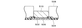
図16は、従来の半導体チップにおけるAuバンプの断面図である。内部の集積回路に繋がる配線の一部であるパッド502は、電気的接続領域の表面を除いてパッシベーション膜504によって被覆されている。
【0005】
まず、アンダーバンプメタル層(バリアメタル層及び密着性金属層の積層)506をスパッタ法により形成する。その後、フォトリソグラフィ技術によりパッド502の電気的接続領域及びその周囲部を露出させたバンプ形成用のレジスト層508を形成する。次に、レジスト層508のパターンに従って電解メッキ法によりAuをメッキ成長させる。その後、レジスト層508を剥離してからメッキ成長したAuをマスクとして、アンダーバンプメタル層506を、その層の種類に応じてウェットエッチングする。その後はアニールなどを経てバンプ510を形成する。各所で適宜洗浄工程も入る。このように、電解メッキ法によるバンプ形成プロセスは長く、よりいっそうの短縮合理化が要求されている。
【0006】
そこで、最近提案されているのが、無電解メッキ法によるバンプの形成である。無電解メッキ法で形成したバンプは、少なくともアンダーバンプメタル層のスパッタ形成及びエッチング工程が不要である。また、メッキ成長用のレジストの形成が省略できることが期待されている。これにより、大幅なプロセスの短縮が可能で、安価なバンプの形成が実現される。
【0007】
従来、無電解メッキ法でバンプを形成するときには、アルミパッドに、メッキの前処理としていわゆるジンケート処理を施す。すなわち、Znイオンの入った処理液に半導体ウエハを浸漬し、
2Al+3Zn2+→2Al3++3Zn
の反応により、パッド表面をZnに置換する。そして、半導体ウエハ全体をメッキ液(メッキに関する処理液)に浸漬して、メッキ金属を析出する。なお、複数枚の半導体ウエハをメッキ液に浸漬するバッジ処理で合理化を図ることができる。
【0008】
GND電極となるアルミパッドは、半導体ウエハのSi基板と電気的に接続されている。Si基板は処理液に電気的に導通し、Si基板の電子が処理液に放出されると、そのアルミパッドの電位が変化する。このようなグランド効果の影響により、化学反応のための電子が減少してしまう結果、イオン結合が起こりにくくなり、ジンケート処理でアルミパッド表面のZnへの置換が不十分となる。同様に、グランド効果の影響によりメッキレートが変化して、メッキ金属の析出に影響を及ぼす。
【0009】
そこで、グランド効果の影響を防ぐために、半導体ウエハ裏面及び周縁部近傍(半導体ウエハ表面の外周部から側部にかけて)にレジストを相当量厚く塗布することがある。こうすることで、メッキに関する処理液が半導体ウエハ周縁部近傍及び裏面に接触しないようにしてから、ジンケート処理及びメッキ処理を行う。
【0010】
半導体ウエハ裏面へのレジスト塗布は、スピンコーターの回転テーブルにバンプ形成面(半導体ウエハ主面)をチャック(真空吸着)して行う。その場合、その後のメッキ成長に影響を与えないように、バンプ形成面に傷が付かないようにしなければならない。また、半導体ウエハ裏面にレジストを塗布しても、パッドが電気的に接続される部位の電位に応じてメッキ金属の析出成長が決まるので、均等な高さで高品質の無電解メッキバンプを形成することが難しかった。
【0011】
本発明は、半導体ウエハ、バンプ付き半導体ウエハの製造方法、バンプ付き半導体チップ及びその製造方法、半導体装置、回路基板並びに電子機器に関して、高品質の無電解メッキを行うことを目的とする。
【0012】
【課題を解決するための手段】
本発明に係る半導体ウエハは、複数の半導体チップの機能を実現するために半導体結晶体に作り込まれてなる複数のモノリシック集積回路と、
前記複数の半導体チップにするための複数の第1の領域に形成されてなる複数のパッドと、
前記パッドよりも下層側に位置して、2つの前記第1の領域間の第2の領域を通って、2つ以上の前記パッドを電気的に接続する導電体と、
少なくとも前記第2の領域を含む領域に形成され、前記半導体結晶体に作り込まれてなる、前記半導体結晶体とは逆の導電型の不純物拡散領域と、
を有し、
前記導電体は、前記半導体結晶体の前記不純物拡散領域以外の部分を避けて、前記不純物拡散領域に電気的に接続されてなる。
【0013】
本発明によれば、2つ以上のパッドが電気的に接続されており、電位差が小さい又は電位差がないので、高品質の無電解メッキを行うことができる。
【0046】
【発明の実施の形態】
以下、本発明の実施の形態を、図面を参照して説明する。
【0047】
(実施の形態)
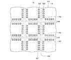
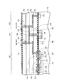
図1は、本発明の実施の形態に係る半導体ウエハの平面の一部を示す図である。図2は、本発明の実施の形態に係る半導体ウエハの断面の一部を示す図である。
【0048】
半導体ウエハ10は、複数の半導体チップに切断(例えばダイシング又はスクライビング)されるものである。半導体ウエハ10は、半導体結晶体(例えばSi基板)12を有する。半導体結晶体12は、不純物が添加されており、n型又はp型の導電型を示す。半導体結晶体12には、複数のモノリシック集積回路14が作り込まれている。各モノリシック集積回路14は、各半導体チップの機能を実現するためのものである。
【0049】
図2には、モノリシック集積回路14の素子の1つとして、MOSトランジスタ20が示されている。詳しくは、半導体結晶体12にウェル22が形成されている。ウェル22は、半導体結晶体12とは逆の導電型を示す。ウェル22には、間隔をあけて一対の拡散領域24が形成されており、その一方がソース領域で、他方がドレイン領域である。拡散領域24は、ウェル22とは逆の導電型を示す。ウェル22上には、絶縁膜(例えばSiO2等の酸化膜)26が形成されている。絶縁膜26上であって一対の拡散領域24の間に第1の電極(ゲート電極)28が形成され、一方の拡散領域24上に第2の電極(ソース電極)30が形成され、他方の拡散領域24上に第3の電極(ドレイン電極)32が形成されている。拡散領域24は、不純物が導入された領域であって、その導入方法は、熱拡散プロセスのみならずイオン注入であってもよい。
【0050】
1つの素子は、素子分離領域34によって、他の素子から電気的に絶縁されている。素子分離領域34の形成には、LOCOS(Local Oxidation of Silicon)を適用してもよい。例えば、ウェル22上に形成された絶縁膜26の厚い部分が素子分離領域34であってもよい。また、絶縁膜26上にさらに絶縁膜36が形成されていてもよい。
【0051】
半導体結晶体12には、不純物拡散領域38が形成されていてもよい。不純物拡散領域38は、その外側の領域と電気的に絶縁された状態になっている。不純物拡散領域38は、半導体結晶体12とは逆の導電型を示してもよい。その場合、不純物拡散領域38とその外側の領域との間に空乏層が形成されるなどの理由で、半導体結晶体12及び不純物拡散領域38の間に電流が流れにくくなっている。不純物拡散領域38は、後述する第2の領域44内にのみ形成されていてもよいが、図2に示す例では、第2の領域44を超えて第1の領域42の端部に至るまで形成されている。不純物拡散領域38は、ガードリングであってもよい。
【0052】
半導体結晶体12には、電気的に導通する不純物拡散領域40が形成されていてもよい。不純物拡散領域40は、半導体結晶体12と同じ導電型を示してもよい。その場合、半導体結晶体12及び不純物拡散領域40の間に電流が流れやすくなっている。なお、不純物拡散領域38,40は、不純物が導入された領域であって、その導入方法は、熱拡散プロセスのみならずイオン注入であってもよい。
【0053】
半導体ウエハ10は、複数の半導体チップにするための複数の第1の領域42と、2つの(例えば隣り合う)第1の領域42の間の第2の領域44と、を有する。第2の領域44は、切削ラインであってもよい。第2の領域44は、それぞれの第1の領域42を囲んでいてもよい。全ての第1の領域42内の構造が少なくとも設計上同じであってもよい。
【0054】
半導体ウエハ10は、複数のパッド50を有する。パッド50は、アルミニウムで形成してもよい。パッド50は、第1の領域42に形成されている。図2に示すように、複数のパッド50のうち、第1のパッド52は、モノリシック集積回路14の素子(例えばMOSトランジスタ20)に電気的に接続されている。その電気的接続のための第1の経路54は、深さ又は高さ方向の電気的接続を図るコンタクト層(ビア、プラグを含む。)と、横方向の電気的接続を図る配線を含んでもよい。なお、1つの第1の領域42に、1グループの第1のパッド52が形成されていてもよい。
【0055】
図2に示すように、複数のパッド50のうち、第2のパッド56は、モノリシック集積回路14を避ける第2の経路58によって半導体結晶体12に電気的に接続されている。例えば、第2の経路58は、半導体結晶体12と同じ導電型の不純物拡散領域40に電気的に接続されていてもよい。不純物拡散領域40によって、第2の経路58及び半導体結晶体12の間に電流が流れやすくなっている。なお、1つの第1の領域42内に、第1及び第2のパッド52,56の両方が形成されていてもよく、全ての第1の領域42内の構造が少なくとも設計上同じであってもよい。
【0056】
半導体ウエハ10は、2つ以上のパッド50を電気的に接続する導電体60を有する。導電体60は、パッド50よりも下層側に位置する。導電体60は、上述した第1及び第2の経路54,58を電気的に接続している。導電体60は、2つの第1の領域42間の第2の領域44を通る。第2の領域44で半導体ウエハ10が切断されると、導電体60の一部が切断面に露出する。この露出面とパッド50とを接続するパスラインが長ければ、パッド50に対してのマイグレーションを防止することができる。そのため、導電体60の、第2の領域44を通る部分(例えば第2の部分64)とパッド50の間に、他の部材(例えば絶縁層70)が介在していてもよい。
【0057】
導電体(例えば配線パターン)60は、第1の部分(例えば共通配線)62を有する。図1に示すように、第1の部分62は、それぞれの第1の領域42を囲むように形成されており、第2の領域44に沿って形成されおり、第2の領域44の内側に形成されている。導電体60は、複数の第2の部分(例えば接続経路)64を有する。それぞれの第2の部分64は、第2の領域44を境として隣り合う一対のパッド50(例えば、図2に示すパッド52、56)を電気的に接続している。また、それぞれの第2の部分64は、第1の部分62に電気的に接続部されている。その電気的接続には、コンタクト層(ビア、プラグを含む。)が使用されていてもよい。
【0058】
導電体60は、第2の領域44に位置する部分が切断されると2つ以上のパッド50(例えば、図2に示すパッド52、56)が電気的に断ち切られるように形成されていてもよい。図2に示す例では、第1の部分62が第2の領域44に位置し、第2の部分64の一部が第2の領域44に位置している。導電体60は、第2の領域44内に、電気的に接続された2つ以上のパッド50のそれぞれへの分岐部66を有していてもよい。分岐部66が除去されると、2つ以上のパッド50(例えば、図2に示すパッド52、56)が電気的に断ち切られる。
【0059】
導電体60は、半導体結晶体12とは電気的に絶縁されていてもよい。例えば、導電体60は、半導体結晶体12とは逆の導電型の不純物拡散領域38に電気的に接続されていてもよい。不純物拡散領域38とその外側の領域との間に空乏層が形成されるなどの理由で、導電体60及び不純物拡散領域38の間に電流が流れにくくなっている。その場合、導電体60は、半導体結晶体12の不純物拡散領域38以外の領域を避けて形成する。導電体60の不純物拡散領域38との電気的接続部分(例えば、第3の部分)68は、コンタクト層(ビア、プラグを含む。)であってもよい。
【0060】
導電体60は、1層又は図2に示す例では複数層の絶縁層70の内部に形成されている。導電体60は、複数の絶縁層70の間に形成されてなる配線と、絶縁層70を貫通するコンタクトホール(ビアホールを含む。)に形成されたコンタクト層(ビア、プラグを含む。)と、を有していてもよい。
【0061】
半導体ウエハ10は、パッシベーション膜72を有する。パッシベーション膜72は、各パッド50の少なくとも中央部を避けて形成されている。パッシベーション膜72は、各パッド50の端部(例えば周縁部)を覆っていてもよい。図2に示す例とは異なるが、パッシベーション膜72は、半導体ウエハ10を切断するためのライン(例えばダイシングライン又はスクライブライン)上を避けて形成してもよい。パッシベーション膜72は、SiO2、SiN、ポリイミド等の樹脂などで形成することができる。パッシベーション膜72は、単層で形成してもよいし、複数層で形成してもよい。
【0062】
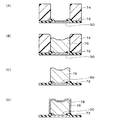
本実施の形態では、上述した半導体ウエハ10にバンプを形成する。本実施の形態では、無電解メッキによってパッド50にバンプを形成する。そのために、図3(A)に示すように、半導体ウエハ10(例えばパッシベーション膜72)上にレジスト層74を形成する。レジスト層74は、パッド50の一部(例えば中央部)を露出させるように形成されている。すなわち、レジスト層74には、パッド50の一部を露出させる開口が形成されている。レジスト層74は、パッシベーション膜72の、パッド50の一部(例えば端部)を覆う部分上に載っていてもよい。このようにパターニングされたレジスト層74は、メッキの成長方向を規制する。メッキの横方向への成長をレジスト層74によって規制するので、幅小さい又は狭ピッチのバンプを形成することができる。また、半導体ウエハ10は、洗浄工程などを経ている。
【0063】
無電解メッキでは、例えば、ジンケート処理を行う。図3(A)に示すように、ジンケート処理により、パッド50の表面にZnを置換する。すなわち、
2Al+3Zn2+→2Al3++3Zn
の反応によりZnを置換する。
【0064】
本実施の形態では、上述したように、2つ以上のパッド50が電気的に接続されている。例えば、半導体結晶体12から電気的に絶縁された第1のパッド54と、半導体結晶体12に電気的に接続された第2パッド56とが電気的に接続されている。したがって、第1及び第2のパッド54,56は、同電位となっているので、ジンケート処理の程度に著しい差が生じない。すなわち、グランド効果の影響が少なく、全てのパッド50に対して均等にジンケート処理を行うことができる。なお、第1のパッド54は、第2の経路58を経由してのみ半導体結晶体12と電気的に接続されるので、第1のパッド54から半導体結晶体12へ電子が逃げることは少ない。また、グランド効果の影響が少ないので、半導体ウエハ10の裏面へのレジスト塗布工程も不要であり、レジスト塗布工程で懸念される、半導体ウエハ10のパッド50が形成された面(主表面)へのダメージもなくすことができる。
【0065】
なお、本発明は、主表面以外の面(例えば裏面)にレジストを塗布することを除外するものではない。あるいは、主表面のみがジンケート処理液に触れるようなカップ式の処理槽を使用して、ジンケート処理液が主表面以外の面に触れないようにしてもよい。
【0066】
次に、図3(B)に示すように、金属(例えばNi)の析出を行う。半導体ウエハ10に処理液(例えば無電解メッキ液)を接触させる。無電解Niメッキを行う場合、ジンケート処理したパッド50の表面ではZnとNiの置換反応が起こる。すなわち、NiとZnのイオン化傾向の違いで置換メッキが行われる。次いで、Ni上に、
Ni2++2H2PO2-→2H2PO3-+Ni+2H+H2
の反応により、Niを析出することができる。その他の内容及び作用効果については、ジンケート処理について説明した内容が該当する。全てのパッド50に対して均等にNiメッキを行ってバンプ76を形成することができる。
【0067】
次に、図3(C)に示すように、レジスト層74を除去する。必要であれば、図3(D)に示すように、パッド50上の1層からなるバンプ76に他の金属(例えばAu)の析出を行ってもよい。半導体ウエハ10に処理液(例えば無電解メッキ液(例えば無電解Auメッキ液))を接触させる。無電解Auメッキを行う場合、バンプ76(Niからなる層)の表面で、NiとAuのイオン化傾向の違いから、
3Ni+2Au3+→3Ni2++2Au
で示される置換メッキが行われる。次いで、置換メッキAu上に、例えばキノン系還元剤を用いて、Auの無電解析出が生じる。その他の内容及び作用効果については、バンプ76を形成するための無電解メッキについて説明した内容が該当する。全てのバンプ76に対して均等にAuメッキを行ってバンプ76の被覆層(第2層)78を形成することができる。Auによって形成された被覆層78は、電気的接続を向上させるだけでなく、Niからなるバンプ76の酸化やマイグレーションに対する耐性の向上にも寄与する。以上の工程によって、バンプ付き半導体ウエハを製造することができる。
【0068】
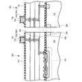
本実施の形態に係るバンプ付き半導体チップの製造方法は、上述した構成を有するバンプ付き半導体ウエハを切断することを含む。例えば、図4に示すように、半導体ウエハ10をツール(ダイサ等のカッタ又はスクライバ)80によって切断する。半導体ウエハ10の切断は、第2の領域44(図1参照)に沿って行う。半導体ウエハ10を切断するときに、第2の領域44を切削し、図2に示す導電体60の第2の領域44内の部分を除去してもよい。第1の部分62の全てを除去してもよい。あるいは、第2の部分64を切断するようにその一部を除去してもよい。半導体ウエハ10を切断することで、導電体60による2つ以上のパッド50の電気的接続を断ち切ってもよい。こうして、個々のバンプ付き半導体チップを得ることができる。
【0069】
図5は、上述した方法によって製造されたバンプ付き半導体チップを示す図である。半導体チップ90は、上述した半導体ウエハ10の第1の領域42内の構造を有する。また、パッド50上にバンプ76が設けられ、その表面に被覆層78が形成されている。詳しくは、上述した通りである。
【0070】
半導体チップ90は、導電体60(例えばその第2の部分64)の切断面が露出している。導電体60の、第2の領域44を通る部分(例えば第2の部分64)がパッド50よりも下層に形成されているので、露出面とパッド50とを接続するパスラインが長くなり、パッド50に対してのマイグレーションを防止することができる。また、半導体チップ90は、不純物拡散領域38の切断面が露出していてもよい。
【0071】
図6は、本実施の形態に係る半導体装置を示す図である。半導体装置は、半導体チップ90を有する。半導体チップ90は、基板(例えばセラミック基板又はフレキシブル基板等)92に実装(例えばフェースダウンボンディング)されている。基板92には配線パターン94が形成されている。配線パターン94とバンプ76とが電気的に接続されている。電気的接続に、異方性導電材料(異方性導電膜又は異方性導電ペースト)、導電性材料(導電性ペースト等)を使用してもよいし、金属接合を適用してもよいし、絶縁性接着剤を使用してもよい。基板92には、外部端子(例えばハンダボール)96が設けられていてもよい。
【0072】
図7は、本実施の形態に係るバンプ付き半導体チップが実装された回路基板を示す図である。回路基板(マザーボード)100には、上述した半導体チップ90が実装(例えばフリップチップボンディング)されている。なお、回路基板100には、図示しない配線パターンが形成されている。
【0073】
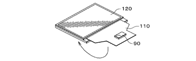
図8は、本実施の形態に係る半導体チップが実装された半導体装置を示す図である。半導体装置は、半導体チップ90が基板110に実装されて、TCP(Tape Carrier Package)を構成している。この半導体装置は、電子パネル(例えば液晶パネルやエレクトロルミネッセンスパネル)120に接合されている。なお、半導体チップ90の実装形態は、COG(Chip On Glass)、COF(Chip On
Film/Flexible)であってもよい。
【0074】
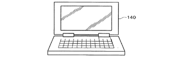
図9には、図6に示す半導体装置が実装された回路基板130が示されている。本発明を適用した半導体装置を有する電子機器として、図10にはノート型パーソナルコンピュータ140、図11には携帯電話150が示されている。
【0075】
(第1の参考例)
図12は、本発明の第1の参考例に係る半導体ウエハを示す図である。本参考例では、半導体結晶体12上に形成された電気的な絶縁体(例えば、絶縁膜26,36、絶縁層70)によって、導電体200と半導体結晶体12が、電気的に絶縁されている。この点を除き、本参考例には、実施の形態で説明した内容が該当する。本参考例でも、実施の形態で説明した作用効果を達成することができる。
【0076】
(第2の参考例)
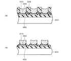
図13(A)〜図13(B)は、本発明の第2の参考例に係るバンプ付き半導体ウエハの製造方法を説明する図である。本参考例で使用する半導体ウエハ300は、図2に示す半導体ウエハ10から導電体60及び不純物拡散領域38を除いた構造を有する。半導体ウエハ300の複数のパッド302上に、2つ以上のパッド302を電気的に接続するように導電膜304を形成する。そして、無電解メッキによって、それぞれのパッド302の上方であって導電膜302上にバンプ310を形成する。導電膜304は、アンダーバンプメタルであってもよい。
【0077】
詳しくは、図13(A)に示すように、パターニングされたレジスト層306を形成する。そして、無電解メッキを行ってバンプ310を形成する。詳しくは、実施の形態で説明した。次に、図13(B)に示すように、レジスト層306を除去し、バンプ310をマスクとして、導電膜304をエッチングする。こうして、バンプ310同士の電気的接続を断ち切ることができる。
【0078】
本参考例でも、実施の形態で説明したように、2つ以上のパッド302を電気的に接続して無電解メッキを行うので、グランド効果の影響を減らすことができる。なお、本参考例の内容を、実施の形態又は他の参考例に適用してもよい。
【0079】
(第3の参考例)
図14は、本発明の第3の参考例に係る半導体ウエハを示す図である。また、図15は、本発明の第3の参考例に係るバンプ付き半導体ウエハの製造方法及びバンプ付き半導体チップの製造方法を説明する図である。
【0080】
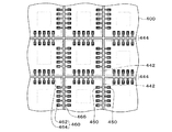
半導体ウエハ400は、図2に示す半導体ウエハ10の導電体60及び不純物拡散領域38を除いた構造を有する。例えば、半導体ウエハ400は、複数の半導体チップの機能を実現するために半導体結晶体412に作り込まれてなる複数のモノリシック集積回路414を有する。半導体ウエハ400は、複数の半導体チップにするための複数の第1の領域442に形成されてなる複数のパッド450を有する。
【0081】
半導体ウエハ400は、導電膜460を有する。導電膜460は、実施の形態で説明した導電体60の代わりに形成されるものであり、導電体60と同じ機能を有していてもよい。例えば、導電膜460は、2つの第1の領域442間の第2の領域444を通るように形成されている。導電膜460は、2つ以上のパッド450(例えば、モノリシック集積回路414に電気的に接続された第1のパッド452と、半導体結晶体412に電気的に接続された第2のパッド456)を電気的に接続するように複数のパッド450上に形成されてなる。
【0082】
導電膜460は、第2の領域444内に、電気的に接続された2つ以上のパッド450のそれぞれへの分岐部466を有していてもよい。導電膜460は、第1の部分462を有していてもよい。第1の部分462は、それぞれの第1の領域442を囲むように第2の領域444に沿って第2の領域444の内側に形成されていてもよい。導電膜460は、複数の第2の部分464を有していてもよい。それぞれの第2の部分464は、パッド450のうち第2の領域444を境として隣り合う一対のパッド450を電気的に接続し、第1の部分462に電気的に接続部されていてもよい。導電膜460は、第2の領域460に位置する部分が切断されると2つ以上のパッド450が電気的に断ち切られるように形成されていてもよい。
【0083】
半導体ウエハ400には、パッド450の上方であって導電膜460上にバンプ476(図15参照)を形成することができる。その形成方法は、実施の形態で説明した通りである。導電膜460は、アンダーバンプメタルであってもよい。
【0084】
そして、図15に示すように、半導体ウエハ400を切断して、バンプ付き半導体チップを製造することができる。その詳細は、実施の形態で説明した通りである。図15に示すバンプ付き半導体チップ490は、導電膜460の切断面が露出している。
【0085】
本参考例でも、実施の形態で説明したように、2つ以上のパッド450を電気的に接続して無電解メッキを行うので、グランド効果の影響を減らすことができる。なお、本参考例の内容を、実施の形態又は他の参考例に適用してもよい。
【0086】
本発明は、上述した実施の形態に限定されるものではなく、種々の変形が可能である。例えば、本発明は、実施の形態で説明した構成と実質的に同一の構成(例えば、機能、方法及び結果が同一の構成、あるいは目的及び結果が同一の構成)を含む。また、本発明は、実施の形態で説明した構成の本質的でない部分を置き換えた構成を含む。また、本発明は、実施の形態で説明した構成と同一の作用効果を奏する構成又は同一の目的を達成することができる構成を含む。また、本発明は、実施の形態で説明した構成に公知技術を付加した構成を含む。
【図面の簡単な説明】
【図1】 図1は、本発明の実施の形態に係る半導体ウエハの平面の一部を示す図である。
【図2】 図2は、本発明の実施の形態に係る半導体ウエハの断面の一部を示す図である。
【図3】 図3(A)〜図3(D)は、本発明の実施の形態に係るバンプ付き半導体ウエハの製造方法を説明する図である。
【図4】 図4は、本発明の実施の形態に係るバンプ付き半導体チップの製造方法を説明する図である。
【図5】 図5は、本発明の実施の形態に係るバンプ付き半導体チップ及びその製造方法を示す図である。
【図6】 図6は、本発明の実施の形態に係る半導体装置を示す図である。
【図7】 図7は、本発明の実施の形態に係るバンプ付き半導体チップが実装された回路基板を示す図である。
【図8】 図8は、本発明の実施の形態に係る半導体チップが実装された半導体装置を示す図である。
【図9】 図9は、図6に示す半導体装置が実装された回路基板を示す図である。
【図10】 図10は、本発明の実施の形態に係る半導体装置を有する電子機器を示す図である。
【図11】 図11は、本発明の実施の形態に係る半導体装置を有する電子機器を示す図である。
【図12】 図12は、本発明の第1の参考例に係る半導体ウエハを示す図である。
【図13】 図13(A)〜図13(B)は、本発明の第2の参考例に係るバンプ付き半導体ウエハの製造方法を説明する図である。
【図14】 図14は、本発明の第3の参考例に係る半導体ウエハを示す図である。
【図15】 図15は、本発明の第3の参考例に係るバンプ付き半導体ウエハの製造方法及びバンプ付き半導体チップの製造方法を説明する図である。
【図16】 図16は、本発明の従来技術を説明する図である。
【符号の説明】
10 半導体ウエハ
12 半導体結晶体
14 モノリシック集積回路
38 不純物拡散領域
42 第1の領域
44 第2の領域
50 パッド
52 第1のパッド
54 第1の経路
56 第2のパッド
58 第2の経路
60 導電体
62 第1の部分
64 第2の部分
66 分岐部
76 バンプ
90 半導体チップ[0001]
BACKGROUND OF THE INVENTION
The present invention relates to a semiconductor wafer, a method for manufacturing a semiconductor wafer with bumps, a semiconductor chip with bumps and a method for manufacturing the same, a semiconductor device, a circuit board, and an electronic apparatus.
[0002]
BACKGROUND OF THE INVENTION
As semiconductor integrated circuits become highly integrated and semiconductor chips shrink, packaging technology that can handle terminal connections with a fine pitch is required. Mounting techniques that easily meet this requirement include TAB (Tape Automated Bonding) mounting used in TCP (Tape Carrier Package) and flip chip mounting used in CSP (Chip Size Package) and the like.
[0003]
In the mounting technology as described above, bumps are usually provided on pads of a semiconductor chip. The bump is typically an Au bump, for example, and is generally formed by electrolytic plating. A method for forming Au bump electrodes by electrolytic plating will be described below.
[0004]
FIG. 16 is a cross-sectional view of an Au bump in a conventional semiconductor chip. A
[0005]
First, an under bump metal layer (lamination of a barrier metal layer and an adhesive metal layer) 506 is formed by sputtering. Thereafter, a
[0006]
Therefore, recently proposed is bump formation by an electroless plating method. The bump formed by the electroless plating method does not require at least the sputter formation and etching process of the under bump metal layer. In addition, it is expected that the formation of resist for plating growth can be omitted. As a result, the process can be greatly shortened, and inexpensive bump formation can be realized.
[0007]
Conventionally, when bumps are formed by an electroless plating method, a so-called zincate treatment is applied to an aluminum pad as a pretreatment for plating. That is, the semiconductor wafer is immersed in a treatment liquid containing Zn ions,
2Al + 3Zn2+→ 2Al3++ 3Zn
By this reaction, the pad surface is replaced with Zn. Then, the entire semiconductor wafer is immersed in a plating solution (a treatment solution relating to plating) to deposit a plating metal. In addition, rationalization can be achieved by a badge process in which a plurality of semiconductor wafers are immersed in a plating solution.
[0008]
The aluminum pad serving as the GND electrode is electrically connected to the Si substrate of the semiconductor wafer. The Si substrate is electrically connected to the processing liquid, and when the electrons of the Si substrate are released to the processing liquid, the potential of the aluminum pad changes. As a result of the influence of such a ground effect, the number of electrons for the chemical reaction is reduced. As a result, ionic bonding is less likely to occur, and the zinc pad surface is not sufficiently substituted with Zn on the surface of the aluminum pad. Similarly, the plating rate changes due to the influence of the ground effect, which affects the deposition of the plating metal.
[0009]
Therefore, in order to prevent the influence of the ground effect, a considerable amount of resist may be applied to the back surface of the semiconductor wafer and the vicinity of the peripheral portion (from the outer peripheral portion to the side portion of the semiconductor wafer surface). By doing so, the zincate treatment and the plating treatment are performed after the treatment liquid relating to the plating does not come into contact with the vicinity of the peripheral edge of the semiconductor wafer and the back surface.
[0010]
The resist coating on the back surface of the semiconductor wafer is performed by chucking (vacuum suction) the bump forming surface (semiconductor wafer main surface) on a rotary table of a spin coater. In that case, it is necessary to prevent the bump forming surface from being damaged so as not to affect the subsequent plating growth. Even if resist is applied to the backside of the semiconductor wafer, the deposition growth of plating metal is determined according to the potential of the part where the pad is electrically connected, so high-quality electroless plating bumps are formed at a uniform height. It was difficult to do.
[0011]
An object of the present invention is to perform high-quality electroless plating with respect to a semiconductor wafer, a method for manufacturing a semiconductor wafer with bumps, a semiconductor chip with bumps and a manufacturing method thereof, a semiconductor device, a circuit board, and an electronic device.
[0012]
[Means for Solving the Problems]
A semiconductor wafer according to the present invention includes a plurality of monolithic integrated circuits formed in a semiconductor crystal to realize the functions of a plurality of semiconductor chips,
A plurality of pads formed in a plurality of first regions for forming the plurality of semiconductor chips;
A conductor located on a lower layer side than the pads, passing through a second region between the two first regions, and electrically connecting two or more of the pads;
An impurity diffusion region having a conductivity type opposite to that of the semiconductor crystal, formed in a region including at least the second region, and formed in the semiconductor crystal;
HaveAnd
The conductor is electrically connected to the impurity diffusion region while avoiding portions other than the impurity diffusion region of the semiconductor crystal body..
[0013]
According to the present invention, since two or more pads are electrically connected and the potential difference is small or there is no potential difference, high-quality electroless plating can be performed.
[0046]
DETAILED DESCRIPTION OF THE INVENTION
Hereinafter, embodiments of the present invention will be described with reference to the drawings.
[0047]
(Embodiment)
FIG. 1 illustrates the present invention.EmbodimentIt is a figure showing a part of plane of a semiconductor wafer concerning. FIG. 2 illustrates the present invention.EmbodimentIt is a figure showing a part of section of a semiconductor wafer concerning.
[0048]
The
[0049]
FIG. 2 shows a
[0050]
One element is electrically isolated from other elements by the
[0051]
An
[0052]
An
[0053]
The
[0054]
The
[0055]
As shown in FIG. 2, among the plurality of
[0056]
The
[0057]
The conductor (for example, a wiring pattern) 60 has a first portion (for example, a common wiring) 62. As shown in FIG. 1, the
[0058]
Even if the
[0059]
The
[0060]
The
[0061]
The
[0062]
In the present embodiment, bumps are formed on the
[0063]
In electroless plating, for example, a zincate process is performed. As shown in FIG. 3A, Zn is substituted on the surface of the
2Al + 3Zn2+→ 2Al3++ 3Zn
Zn is substituted by the reaction.
[0064]
In the present embodiment, as described above, two or
[0065]
In addition, this invention does not exclude applying a resist to surfaces (for example, back surface) other than the main surface. Alternatively, a cup-type treatment tank in which only the main surface touches the zincate treatment liquid may be used so that the zincate treatment liquid does not touch any surface other than the main surface.
[0066]
Next, as shown in FIG. 3B, metal (for example, Ni) is deposited. A treatment liquid (for example, electroless plating liquid) is brought into contact with the
Ni2++ 2H2PO2-→ 2H2PO3-+ Ni + 2H + H2
Ni can be precipitated by this reaction. About the other content and effect, the content demonstrated about the zincate process corresponds. The
[0067]
Next, as shown in FIG. 3C, the resist
3Ni + 2Au3+→ 3Ni2++ 2Au
Substitution plating shown by is performed. Next, electroless deposition of Au occurs on the displacement plating Au using, for example, a quinone-based reducing agent. For the other contents and effects, the contents described for the electroless plating for forming the
[0068]
The method for manufacturing a semiconductor chip with bumps according to the present embodiment includes cutting the semiconductor wafer with bumps having the above-described configuration. For example, as shown in FIG. 4, the
[0069]
FIG. 5 is a diagram showing a semiconductor chip with bumps manufactured by the method described above. The
[0070]
In the
[0071]
FIG. 6 shows a semiconductor device according to the present embodiment. The semiconductor device has a
[0072]
FIG. 7 is a diagram showing a circuit board on which the bumped semiconductor chip according to the present embodiment is mounted. The above-described
[0073]
FIG. 8 is a diagram showing a semiconductor device on which the semiconductor chip according to the present embodiment is mounted. In the semiconductor device, a
Film / Flexible).
[0074]
FIG. 9 shows a
[0075]
(First reference example)
FIG. 12 illustrates the present invention.First reference exampleIt is a figure which shows the semiconductor wafer which concerns on. BookReference exampleThen, the
[0076]
(Second reference example)
13 (A) to 13 (B) show the present invention.Second reference exampleIt is a figure explaining the manufacturing method of the semiconductor wafer with a bump concerning. BookReference
[0077]
Specifically, as shown in FIG. 13A, a patterned resist
[0078]
BookReference exampleButEmbodimentAs described above, since the electroless plating is performed by electrically connecting two or
[0079]
(Third reference example)
FIG. 14 illustrates the present invention.Third reference exampleIt is a figure which shows the semiconductor wafer which concerns on. In addition, FIG.Third reference exampleIt is a figure explaining the manufacturing method of the semiconductor wafer with a bump which concerns on, and the manufacturing method of the semiconductor chip with a bump.
[0080]
The
[0081]
The
[0082]
The
[0083]
On the
[0084]
And as shown in FIG. 15, the
[0085]
BookReference exampleButEmbodimentAs described above, since the electroless plating is performed by electrically connecting two or
[0086]
The present invention is not limited to the above-described embodiments, and various modifications can be made. For example, the present invention includes configurations that are substantially the same as the configurations described in the embodiments (for example, configurations that have the same functions, methods, and results, or configurations that have the same purposes and results). In addition, the invention includes a configuration in which a non-essential part of the configuration described in the embodiment is replaced. In addition, the present invention includes a configuration that exhibits the same operational effects as the configuration described in the embodiment or a configuration that can achieve the same object. Further, the invention includes a configuration in which a known technique is added to the configuration described in the embodiment.
[Brief description of the drawings]
FIG. 1 illustrates the present invention.EmbodimentIt is a figure showing a part of plane of a semiconductor wafer concerning.
FIG. 2 illustrates the present invention.EmbodimentIt is a figure showing a part of section of a semiconductor wafer concerning.
3 (A) to 3 (D) are views of the present invention.EmbodimentIt is a figure explaining the manufacturing method of the semiconductor wafer with a bump concerning.
FIG. 4 is a diagram of the present invention.EmbodimentIt is a figure explaining the manufacturing method of the semiconductor chip with a bump concerning.
FIG. 5 is a diagram of the present invention.EmbodimentIt is a figure which shows the semiconductor chip with a bump which concerns on, and its manufacturing method.
FIG. 6 is a diagram of the present invention.EmbodimentIt is a figure which shows the semiconductor device which concerns on.
FIG. 7 is a diagram showing a circuit board on which a bumped semiconductor chip according to an embodiment of the present invention is mounted.
FIG. 8 is a diagram showing a semiconductor device on which a semiconductor chip according to an embodiment of the present invention is mounted.
FIG. 9 is a diagram illustrating a circuit board on which the semiconductor device illustrated in FIG. 6 is mounted.
FIG. 10 is a diagram showing an electronic apparatus having the semiconductor device according to the embodiment of the present invention.
FIG. 11 is a diagram showing an electronic apparatus having the semiconductor device according to the embodiment of the present invention.
FIG. 12 is a diagram of the present invention.First reference exampleIt is a figure which shows the semiconductor wafer which concerns on.
13 (A) to 13 (B) are diagrams of the present invention.Second reference exampleIt is a figure explaining the manufacturing method of the semiconductor wafer with a bump concerning.
FIG. 14 is a diagram of the present invention.Third reference exampleIt is a figure which shows the semiconductor wafer which concerns on.
FIG. 15 is a diagram of the present invention.Third reference exampleIt is a figure explaining the manufacturing method of the semiconductor wafer with a bump which concerns on, and the manufacturing method of the semiconductor chip with a bump.
FIG. 16 is a diagram for explaining the prior art of the present invention.
[Explanation of symbols]
10 Semiconductor wafer
12 Semiconductor crystal
14 Monolithic integrated circuit
38 Impurity diffusion region
42 First region
44 Second area
50 pads
52 First pad
54 First route
56 Second pad
58 Second Route
60 Conductor
62 First part
64 Second part
66 Bifurcation
76 Bump
90 Semiconductor chip
Claims (6)
前記複数の半導体チップにするための複数の第1の領域に形成されてなる複数のパッドと、
前記パッドよりも下層側に位置して、2つの前記第1の領域間の第2の領域を通って、2つ以上の前記パッドを電気的に接続する導電体と、
少なくとも前記第2の領域を含む領域に形成され、前記半導体結晶体に作り込まれてなる、前記半導体結晶体とは逆の導電型の不純物拡散領域と、
を有し、
前記導電体は、前記半導体結晶体の前記不純物拡散領域以外の部分を避けて、前記不純物拡散領域に電気的に接続されてなる半導体ウエハ。A plurality of monolithic integrated circuits formed in a semiconductor crystal to realize the functions of a plurality of semiconductor chips;
A plurality of pads formed in a plurality of first regions for forming the plurality of semiconductor chips;
A conductor located on a lower layer side than the pads, passing through a second region between the two first regions, and electrically connecting two or more of the pads;
An impurity diffusion region having a conductivity type opposite to that of the semiconductor crystal, formed in a region including at least the second region, and formed in the semiconductor crystal;
Have
A semiconductor wafer in which the conductor is electrically connected to the impurity diffusion region while avoiding portions other than the impurity diffusion region of the semiconductor crystal.
前記複数のパッドのうち、第1のパッドは第1の経路によって前記モノリシック集積回路の素子に電気的に接続され、第2のパッドは前記モノリシック集積回路を避ける第2の経路によって前記半導体結晶体に電気的に接続されてなり、
前記導電体は、前記第1及び第2の経路を電気的に接続してなる半導体ウエハ。The semiconductor wafer according to claim 1,
Among the plurality of pads, the first pad is electrically connected to the element of the monolithic integrated circuit by a first path, and the second pad is the semiconductor crystal body by a second path that avoids the monolithic integrated circuit. Is electrically connected to the
The conductor is a semiconductor wafer formed by electrically connecting the first and second paths.
前記第2の領域は、切削ラインである半導体ウエハ。In the semiconductor wafer according to claim 1 or 2,
The second region is a semiconductor wafer which is a cutting line.
前記導電体は、前記第2の領域に位置する部分が切断されると前記2つ以上のパッドが電気的に断ち切られるように形成されてなる半導体ウエハ。In the semiconductor wafer in any one of Claims 1-3,
The semiconductor wafer, wherein the conductor is formed such that the two or more pads are electrically cut when a portion located in the second region is cut.
前記導電体は、第1の部分と、複数の第2の部分と、を有し、
前記第1の部分は、それぞれの前記第1の領域を囲むように前記第2の領域に沿って前記第2の領域の内側に形成されてなり、
それぞれの前記第2の部分は、前記パッドのうち前記第2の領域を境として隣り合う一対のパッドを電気的に接続し、前記第1の部分に電気的に接続部されてなる半導体ウエハ。In the semiconductor wafer in any one of Claims 1-4,
The conductor has a first portion and a plurality of second portions,
The first portion is formed inside the second region along the second region so as to surround each first region,
Each of the second portions is a semiconductor wafer in which a pair of pads adjacent to each other with the second region as a boundary among the pads are electrically connected and electrically connected to the first portion.
電気的に接続された前記2つ以上のパッド上にバンプをさらに有する半導体ウエハ。In the semiconductor wafer according to any one of claims 1 to 5,
A semiconductor wafer further comprising bumps on the two or more pads that are electrically connected.
Priority Applications (2)
| Application Number | Priority Date | Filing Date | Title |
|---|---|---|---|
| JP2002238017A JP4058619B2 (en) | 2001-10-25 | 2002-08-19 | Semiconductor wafer |
| US10/268,835 US6806556B2 (en) | 2001-10-25 | 2002-10-11 | Semiconductor wafer, method of manufacturing semiconductor wafer having bumps, semiconductor chip having bumps and method of manufacturing the same, semiconductor device, circuit board, and electronic equipment |
Applications Claiming Priority (3)
| Application Number | Priority Date | Filing Date | Title |
|---|---|---|---|
| JP2001-327239 | 2001-10-25 | ||
| JP2001327239 | 2001-10-25 | ||
| JP2002238017A JP4058619B2 (en) | 2001-10-25 | 2002-08-19 | Semiconductor wafer |
Publications (2)
| Publication Number | Publication Date |
|---|---|
| JP2003204014A JP2003204014A (en) | 2003-07-18 |
| JP4058619B2 true JP4058619B2 (en) | 2008-03-12 |
Family
ID=26624089
Family Applications (1)
| Application Number | Title | Priority Date | Filing Date |
|---|---|---|---|
| JP2002238017A Expired - Fee Related JP4058619B2 (en) | 2001-10-25 | 2002-08-19 | Semiconductor wafer |
Country Status (2)
| Country | Link |
|---|---|
| US (1) | US6806556B2 (en) |
| JP (1) | JP4058619B2 (en) |
Families Citing this family (21)
| Publication number | Priority date | Publication date | Assignee | Title |
|---|---|---|---|---|
| JP2003203940A (en) * | 2001-10-25 | 2003-07-18 | Seiko Epson Corp | Semiconductor chip, wiring board, and manufacturing method thereof, semiconductor wafer, semiconductor device, circuit board, and electronic equipment |
| JP4049134B2 (en) * | 2004-08-06 | 2008-02-20 | 株式会社村田製作所 | Manufacturing method of electronic parts |
| US8063495B2 (en) | 2005-10-03 | 2011-11-22 | Rohm Co., Ltd. | Semiconductor device |
| JP2007165402A (en) * | 2005-12-09 | 2007-06-28 | Rohm Co Ltd | Semiconductor device |
| JP2008060537A (en) * | 2006-07-31 | 2008-03-13 | Sanyo Electric Co Ltd | Semiconductor device and manufacturing method thereof |
| US20080122039A1 (en) * | 2006-11-02 | 2008-05-29 | United Microelectronics Corp. | Intergrated circuit device, chip, and method of fabricating the same |
| JP4956173B2 (en) * | 2006-12-19 | 2012-06-20 | 新光電気工業株式会社 | Flip chip mounting board |
| US7713861B2 (en) * | 2007-10-13 | 2010-05-11 | Wan-Ling Yu | Method of forming metallic bump and seal for semiconductor device |
| JP4484934B2 (en) * | 2008-02-26 | 2010-06-16 | 富士通メディアデバイス株式会社 | Electronic component and manufacturing method thereof |
| CN102177582B (en) * | 2008-08-07 | 2014-07-09 | 意法半导体股份有限公司 | A circuit used to supply power in parallel during testing of multiple electronic devices integrated on a semiconductor wafer |
| DE102008042107A1 (en) * | 2008-09-15 | 2010-03-18 | Robert Bosch Gmbh | Electronic component and method for its production |
| EP2290686A3 (en) | 2009-08-28 | 2011-04-20 | STMicroelectronics S.r.l. | Method to perform electrical testing and assembly of electronic devices |
| JP5401301B2 (en) | 2009-12-28 | 2014-01-29 | ルネサスエレクトロニクス株式会社 | Semiconductor device manufacturing method and semiconductor device |
| US20110291264A1 (en) * | 2010-06-01 | 2011-12-01 | Daesik Choi | Integrated circuit packaging system with posts and method of manufacture thereof |
| WO2013067659A1 (en) * | 2011-11-11 | 2013-05-16 | Chu Tse-Ming | Bump structure of wafer bonding pad and manufacturing method thereof |
| JP6084139B2 (en) * | 2013-09-05 | 2017-02-22 | オリンパス株式会社 | Semiconductor substrate and manufacturing method thereof |
| JP6436531B2 (en) * | 2015-01-30 | 2018-12-12 | 住友電工デバイス・イノベーション株式会社 | Manufacturing method of semiconductor device |
| US9893058B2 (en) | 2015-09-17 | 2018-02-13 | Semiconductor Components Industries, Llc | Method of manufacturing a semiconductor device having reduced on-state resistance and structure |
| KR102333452B1 (en) * | 2017-09-28 | 2021-12-03 | 삼성전자주식회사 | Semiconductor device and method of manufacturing the same |
| JP7319808B2 (en) | 2019-03-29 | 2023-08-02 | ローム株式会社 | Semiconductor equipment and semiconductor packages |
| US20240038703A1 (en) * | 2022-08-01 | 2024-02-01 | Ati Technologies Ulc | Semiconductor assembly including multiple solder masks |
Family Cites Families (3)
| Publication number | Priority date | Publication date | Assignee | Title |
|---|---|---|---|---|
| US4859312A (en) * | 1987-01-12 | 1989-08-22 | Chevron Research Company | Process for making middle distillates using a silicoaluminophosphate molecular sieve |
| CA2174045C (en) * | 1995-04-24 | 2003-01-28 | John Ivor Hammerman | C8 aromatics isomerization using catalyst containing modified silicoaluminophosphate molecular sieve |
| US6535398B1 (en) * | 2000-03-07 | 2003-03-18 | Fujitsu Limited | Multichip module substrates with buried discrete capacitors and components and methods for making |
-
2002
- 2002-08-19 JP JP2002238017A patent/JP4058619B2/en not_active Expired - Fee Related
- 2002-10-11 US US10/268,835 patent/US6806556B2/en not_active Expired - Fee Related
Also Published As
| Publication number | Publication date |
|---|---|
| US6806556B2 (en) | 2004-10-19 |
| US20030080422A1 (en) | 2003-05-01 |
| JP2003204014A (en) | 2003-07-18 |
Similar Documents
| Publication | Publication Date | Title |
|---|---|---|
| JP4058619B2 (en) | Semiconductor wafer | |
| US5757081A (en) | Surface mount and flip chip technology for total integrated circuit isolation | |
| US4784972A (en) | Method of joining beam leads with projections to device electrodes | |
| US7329562B2 (en) | Process of producing semiconductor chip with surface interconnection at bump | |
| KR100419352B1 (en) | Chip scale surface mount package for semiconductor device and process of fabricating the same | |
| US5767578A (en) | Surface mount and flip chip technology with diamond film passivation for total integated circuit isolation | |
| KR101173075B1 (en) | Methods and apparatus for packaging integrated circuit devices | |
| CN101154577B (en) | Semiconductor device and method of manufacturing the same | |
| TWI232560B (en) | Semiconductor device and its manufacture | |
| TWI263280B (en) | Semiconductor device and fabrication method thereof | |
| JP3137596B2 (en) | Semiconductor structure including self-aligned connector and method of manufacturing the same | |
| TWI286454B (en) | Electrical connector structure of circuit board and method for fabricating the same | |
| JP3759909B2 (en) | Semiconductor device and manufacturing method thereof | |
| JP2003203940A (en) | Semiconductor chip, wiring board, and manufacturing method thereof, semiconductor wafer, semiconductor device, circuit board, and electronic equipment | |
| JP3459234B2 (en) | Semiconductor device and manufacturing method thereof | |
| JPH09500240A (en) | Surface mount and flip chip technology | |
| US20080017993A1 (en) | Semiconductor device and method of manufacturing the same | |
| JP2004273591A (en) | Semiconductor device and manufacturing method thereof | |
| JP2008502156A (en) | Semiconductor device with reduced contact resistance | |
| JP2006319204A (en) | Semiconductor device manufacturing method and semiconductor device | |
| JPH11261010A (en) | Semiconductor device and manufacturing method thereof | |
| US20210028060A1 (en) | Contact fabrication to mitigate undercut | |
| JP2003168700A (en) | Semiconductor wafer, semiconductor device and manufacturing method thereof, circuit board, and electronic apparatus | |
| US10930615B2 (en) | Semiconductor device and method of manufacturing semiconductor device | |
| JP2001274191A (en) | Semiconductor device and method of manufacturing semiconductor device |
Legal Events
| Date | Code | Title | Description |
|---|---|---|---|
| A621 | Written request for application examination |
Free format text: JAPANESE INTERMEDIATE CODE: A621 Effective date: 20050318 |
|
| RD04 | Notification of resignation of power of attorney |
Free format text: JAPANESE INTERMEDIATE CODE: A7424 Effective date: 20051220 |
|
| A977 | Report on retrieval |
Free format text: JAPANESE INTERMEDIATE CODE: A971007 Effective date: 20070207 |
|
| A131 | Notification of reasons for refusal |
Free format text: JAPANESE INTERMEDIATE CODE: A131 Effective date: 20070307 |
|
| A521 | Request for written amendment filed |
Free format text: JAPANESE INTERMEDIATE CODE: A523 Effective date: 20070416 |
|
| A131 | Notification of reasons for refusal |
Free format text: JAPANESE INTERMEDIATE CODE: A131 Effective date: 20070905 |
|
| A521 | Request for written amendment filed |
Free format text: JAPANESE INTERMEDIATE CODE: A523 Effective date: 20071030 |
|
| TRDD | Decision of grant or rejection written | ||
| A01 | Written decision to grant a patent or to grant a registration (utility model) |
Free format text: JAPANESE INTERMEDIATE CODE: A01 Effective date: 20071121 |
|
| A61 | First payment of annual fees (during grant procedure) |
Free format text: JAPANESE INTERMEDIATE CODE: A61 Effective date: 20071204 |
|
| FPAY | Renewal fee payment (event date is renewal date of database) |
Free format text: PAYMENT UNTIL: 20101228 Year of fee payment: 3 |
|
| R150 | Certificate of patent or registration of utility model |
Free format text: JAPANESE INTERMEDIATE CODE: R150 |
|
| FPAY | Renewal fee payment (event date is renewal date of database) |
Free format text: PAYMENT UNTIL: 20101228 Year of fee payment: 3 |
|
| FPAY | Renewal fee payment (event date is renewal date of database) |
Free format text: PAYMENT UNTIL: 20111228 Year of fee payment: 4 |
|
| FPAY | Renewal fee payment (event date is renewal date of database) |
Free format text: PAYMENT UNTIL: 20111228 Year of fee payment: 4 |
|
| FPAY | Renewal fee payment (event date is renewal date of database) |
Free format text: PAYMENT UNTIL: 20121228 Year of fee payment: 5 |
|
| FPAY | Renewal fee payment (event date is renewal date of database) |
Free format text: PAYMENT UNTIL: 20121228 Year of fee payment: 5 |
|
| FPAY | Renewal fee payment (event date is renewal date of database) |
Free format text: PAYMENT UNTIL: 20131228 Year of fee payment: 6 |
|
| LAPS | Cancellation because of no payment of annual fees |