JP4050886B2 - Liquid crystal display - Google Patents
Liquid crystal display Download PDFInfo
- Publication number
- JP4050886B2 JP4050886B2 JP2001283500A JP2001283500A JP4050886B2 JP 4050886 B2 JP4050886 B2 JP 4050886B2 JP 2001283500 A JP2001283500 A JP 2001283500A JP 2001283500 A JP2001283500 A JP 2001283500A JP 4050886 B2 JP4050886 B2 JP 4050886B2
- Authority
- JP
- Japan
- Prior art keywords
- liquid crystal
- crystal display
- external electrode
- display device
- fluorescent lamp
- Prior art date
- Legal status (The legal status is an assumption and is not a legal conclusion. Google has not performed a legal analysis and makes no representation as to the accuracy of the status listed.)
- Expired - Fee Related
Links
Images


Landscapes
- Vessels And Coating Films For Discharge Lamps (AREA)
- Planar Illumination Modules (AREA)
Abstract
Description
【0001】
【発明の属する技術分野】
本発明は、液晶表示装置に係り、特に液晶表示パネルと、この液晶表示パネルに形成された電子潜像を可視化する照明光源を備えた液晶表示装置に関する。
【0002】
【従来の技術】
ノート型コンピユータやディスプレイモニターあるいはテレビ受像機用の高精細、薄型、軽量、かつカラー表示が可能な表示装置として液晶表示装置が広く採用されている。この種の液晶表示装置を構成する液晶表示パネルには、各内面に互いに交差する如く形成された平行電極を形成した一対の基板で液晶層を挟持した液晶表示パネルを用いた単純マトリクス型を用いたものと、一対の基板の一方に画素単位で選択するためのスイッチング素子を有する液晶表示パネルを用いたアクティブマトリクス型液晶表示装置とに大別される。
【0003】
アクティブマトリクス型液晶表示パネルは、ツイステッドネマチック(TN)方式に代表されるように、画素選択用の電極群を上下一対の基板のそれぞれに形成した、所謂縦電界方式(一般に、TN方式と称する)と、画素選択用の電極群が上下一対の基板の一方のみに形成した、所謂横電界方式(一般に、IPS方式と称する)とが知られている。
【0004】
前者のTN方式の液晶表示パネルは、一対(第1の基板(下基板)と第2の基板(上基板)からなる2枚)の基板内で液晶が例えば90°ねじれて配向されており、その液晶表示パネルの上下基板の外面に吸収軸方向をクロスニコル配置し、かつ入射側の吸収軸をラビング方向に平行または交差させた2枚の偏光板を積層している。
【0005】
このようなTN方式アクティブマトリクス型液晶表示パネルは、電圧無印加時で入射光は入射側偏光板で直線偏光となり、この直線偏光は液晶層のねじれに沿って伝播し、出射側偏光板の透過軸が当該直線偏光の方位角と一致している場合は直線偏光は全て出射して白表示となる(所謂、ノーマリオープンモード)。また、電圧印加時は、液晶層を構成する液晶分子軸の平均的な配向方向を示す単位ベクトルの向き(ダイレクター)は基板面と垂直な方向を向き、入射側直線偏光の方位角は変わらないため出射側偏光板の吸収軸と一致するため黒表示となる。(1991年、工業調査会発行「液晶の基礎と応用」参照)。
【0006】
一方、一対の基板の一方にのみ画素選択用の電極群や電極配線群を形成し、当該基板上で隣接する電極間(画素電極と対向電極の間)に電圧を印加して液晶層を基板面と平行な方向にスイッチングするIPS方式の液晶表示パネルでは、電圧無印加時に黒表示となるように偏光板が配置されている(所謂、ノーマリクローズモード)。
【0007】
IPS方式液晶表示パネルの液晶層は、初期状態で基板面と平行なホモジニアス配向で、かつ基板と平行な平面で液晶層のダイレクターは電圧無印加時で電極配線方向と平行または幾分角度を有し、電圧印加時で液晶層のダイレクターの向きが電圧の印加に伴い電極配線方向と垂直な方向に移行し、液晶層のダイレクター方向が電圧無印加時のダイレクター方向に比べて45°電極配線方向に傾斜したとき、当該電圧印加時の液晶層は、まるで1/2波長板のように偏光の方位角を90°回転させ、出射側偏向板の透過軸と偏光の方位角が一致して白表示となる。このIPS方式液晶表示パネルは視野角においても色相やコントラストの変化が少なく、広視野角化が図られるという特徴を有している(特開平5−505247号公報参照)。
【0008】
上記した各種の液晶表示パネルを用いた液晶表示装置では、その液晶表示パネルに形成した電子的な画像(電子潜像)を可視化するために外部から照明を与える必要がある。この照明手段としては、周囲光を用いるパッシブ照明方式と、液晶表示パネルの背面側あるいは表面側に冷陰極蛍光灯や発光ダイオード等の光源を設置するアクティブ照明方式とがある。
【0009】
アクティブ照明方式のうち、液晶表示パネルの表面側に光源を配置する方式(一般に、フロントライト方式と称する)は携帯型の情報機器に多く採用される。一方、パソコンやディスプレイモニターなどの比較的サイズが大きい液晶表示装置では、その液晶表示パネルの背面に光源を配置するのが一般的である(これを一般にバックライトと称する)。
【0010】
ノートパソコン等の薄型化が要求される情報機器では、透明板(導光板と称する)の端縁に外部電極蛍光ランプ(以下、LAMPとも言う)などの線状光源を配置して照明光源を構成している。これを、一般にサイドエッジ型と称している。しかし、近年のディスプレイモニターや動画対応のテレビ受像機等に用いられる液晶表示装置の液晶表示パネルの大型化に伴い、画面の明るさ(輝度)を充分に得るため、かつ画面輝度を均一にするために複数のLAMP等の線状光源を液晶表示パネルの背面直下に配置した照明光源が採用されるようになっている。これを、一般に直下型と称している。
【0011】
上記の線状光源として広く採用されている外部電極蛍光ランプLAMPは、所謂低圧水銀灯(蛍光ランプ)であり、ガラスやセラミックス等の透明無機材料でなる小径の筒状細管の内壁に蛍光体膜を塗布し、不活性ガスと水銀を封入して構成される。封入した水銀を蒸発させて励起する手段として、細管内に少なくとも2つの内部電極を設置して、当該電極間に電圧を印加して放電を発生させる構造とした内部電極方式が一般的である。
【0012】
これに対し、本発明者等は、先に、細管の端部外面あるいは端部と中間部外面に外部電極を設置し、この外部電極に電圧を印加することで生じる電界を水銀の励起エネルギーとして加える外部電極方式を提案した(特願2000−162593号他)。この方式によるランプの一例は、放電管の外壁に一対の電極(所謂外部電極)を離間して設け、この電極間に生じる電界を放電管内に生じる電離気体に容量結合させるため、電界結合型放電ランプ(Electric Field Coupled Discharge Lamp)、又は電界結合型無電極蛍光ランプ(Electric Field Coupled Electrodeless Fluorescent Discharge Lamp)とも呼ばれる。この一対の電極は例えば放電管の両端に設けるが、これらの外部電極間に位置する放電管外壁に別の外部電極を互いに離間させて追加し、3箇所以上に設けた外部電極により放電管内に形成する電界強度を強めてもよい。この外部電極方式は細管内に電極を有せず、したがって、動作中の水銀蒸気がスパッタすることによる水銀の消耗がないため、長寿命であるという特徴を有する。この外部電極方式には、水銀を励起するエネルギーを印加する手段の相違で、電界結合方式、上記電極にマイクロ波を印加するマイクロ波結合方式、あるいは磁界を印加する磁界結合方式などがある。
【0013】
図15は電界結合方式を用いた外部電極方式の蛍光ランプ(以下、外部電極蛍光ランプと呼ぶ)の構造の一例を説明する模式図であり、同図(a)は全体図、同(b)は同(a)の要部拡大断面図を示す。この外部電極蛍光ランプLAMPはガラス製の筒状細管TBの両端部外周に外部電極ED1,ED2を設け、両外部電極の間の領域を出光領域L1としている。なお、外部電極ED1,ED2を設置した領域を、それぞれ端部電極領域L21,L22と呼ぶ。
【0014】
【発明が解決しようとする課題】
各端部電極領域L21,L22と出光領域L1を含む細管TBの内壁に蛍光体膜PHが塗布等の手段で形成されている。この蛍光体膜PHを構成する蛍光体としては、所謂三波長蛍光体が使用されている。その成分は、青色蛍光体として(Sr(CaBa)5 (PO4 )3 Cl:Eu2+、あるいはBaMg2 Al16O27:Eu2+、緑色蛍光体としてLaPO4 :Ce3+,Tb3+、赤色蛍光体としてY2 O3 :Eu3+が代表的である。また、細管TBの内部には水銀HGが封入されている。
【0015】
この外部電極蛍光ランプでは、その動作中の放電により蛍光体膜で水銀HGの消費が生じる。この原因は、前記した蛍光体に含まれる金属成分と水銀とが化合することによるものと考えられる。水銀の消費量は、細管内に電極が存在した場合の電極への水銀蒸気のスパッタによる消費量に比べれば少ない。しかし、このような外部電極方式の外部電極蛍光ランプでは、当該外部電極を設置した領域(端部電極領域)L21,L22における蛍光体膜に黒化現象が生じる。この黒化現象は水銀蒸気が外部電極領域にある蛍光体にスパッタしていることに起因すると考えられ、その分の水銀の消費がなされ、この水銀の消耗が外部電極方式の外部電極蛍光ランプの長寿命化を阻害する要因となっている。
【0016】
なお、内部電極方式の冷陰極蛍光ランプでは、細管内の電極間における放電電流に起因する水銀原子の蛍光体への吸着による発光効率の低下を防止するために、蛍光体膜を保護膜で覆ったものが照明学会研究会資料(2000年1月、MD−00−34)に開示されている。しかし、この資料では、内部電極間での蛍光体膜の劣化を問題としているものであり、外部電極方式の外部電極蛍光ランプにおける当該外部電極の設置領域と水銀の消耗に関しては何ら考慮がなされていない。
【0017】
本発明の目的は、照明光源として用いる外部電極方式の外部電極蛍光ランプにおける水銀消費量を抑制して長寿命化をさらに図った液晶表示装置を提供することにある。
【0018】
上記目的を達成するため、本発明は、照明光源として外部電極方式の外部電極蛍光ランプを用いた液晶表示装置において、封入された水銀のスパッタが最も起こり易い外部電極近傍における蛍光体膜を除去したことを特徴とする。また、外部電極の設置領域に細管を構成するガラスよりも二次電子放出係数が大きく、耐スパッタ性が高い膜を形成したことを特徴とする。さらに、外部電極の設置領域における蛍光体膜をガラスよりも二次電子放出係数が大きく、耐スパッタ性が高い膜で被覆したことを特徴とする。以下、本発明の代表的な構成を記述する。
【0019】
(1)、液晶表示パネルと、前記液晶表示パネルに設置されて当該液晶表示パネルに形成された電子潜像を可視化する照明光源を備えた液晶表示装置であって、
前記照明光源は、少なくとも外面の各端部電極領域のそれぞれに外部電極を備えて前記端部電極領域の間に出光領域を有する筒状細管の前記出光領域の内壁にのみ形成された蛍光体膜を有すると共に、前記筒状細管の内部に水銀を封入した外部電極蛍光ランプを備えた。
【0020】
(2)、液晶表示パネルと、前記液晶表示パネルに設置されて当該液晶表示パネルに形成された電子潜像を可視化する照明光源を備えた液晶表示装置であって、
前記照明光源は、少なくとも外面の各端部電極領域のそれぞれに外部電極を備えて前記端部電極領域の間に出光領域を有し、前記筒状細管の前記出光領域および前記各端部電極領域を含めた内壁に形成された蛍光体膜を有し、前記各端部電極領域の前記蛍光体膜を覆って前記端部電極領域の内壁に二次電子放出係数が高く、かつ耐スパッタ性が大きい物質膜を有すると共に、前記筒状細管の内部に水銀を封入した外部電極蛍光ランプを備えた。
【0021】
(3)、液晶表示パネルと、前記液晶表示パネルに設置されて当該液晶表示パネルに形成された電子潜像を可視化する照明光源を備えた液晶表示装置であって、
前記照明光源は、端部の各端部電極領域のそれぞれの外面に設けた端部電極と、前記各端部電極の間の外面の中間電極領域に設けた少なくとも1つの中間電極とを備えて前記各端部電極領域と前記中間電極領域の間に出光領域を有する筒状細管の前記出光領域の内壁にのみ蛍光体膜が形成されると共に、前記筒状細管の内部に水銀を封入した外部電極蛍光ランプを備えた。
【0022】
(4)、(1)〜(3)における前記筒状細管の前記端部電極領域の内壁に二次電子放出係数が高い耐スパッタ性膜として、例えば酸化マグネシウムを用いる。また、前記筒状細管に不活性ガスを封入する。
【0023】
(5)、(1)〜(4)において、前記液晶表示パネルに設置する照明光源が、前記液晶表示パネルの直下に前記外部電極蛍光ランプを複数配列した直下型光源とした。
【0024】
(6)、(1)〜(4)において、前記液晶表示パネルに設置する照明光源が、導光板の側縁に沿って前記外部電極蛍光ランプを設置したサイドエッジ型光源とした。
【0025】
以上の各構成とすることにより、照明光源として用いる外部電極方式の外部電極蛍光ランプにおける水銀消費量を抑制して長寿命化をさらに図った液晶表示装置を提供することができる。なお、本発明は、上記の各構成および後述する実施例の構成に限定されるものではなく、本発明の技術思想を逸脱することなく種々の変形が可能である。
【0026】
【発明の実施の形態】
以下、本発明の実施の形態について、実施例の図面を参照して詳細に説明する。図1は本発明による液晶表示装置の第1実施例の照明光源を構成する外部電極蛍光ランプの模式図である。同図(a)は全体図、同(b)は同(a)の要部拡大断面図を示す。この外部電極蛍光ランプLAMPはガラス製の筒状細管TBの両端部外周に端部電極ED1,ED2を設けている。両端部電極ED1,ED2の間の領域L1は出光領域、両端部電極ED1,ED2を設けた領域はそれぞれ端部電極領域L21,L22である。
【0027】
図1において、細管TBの両端の端部電極領域L21,L22の外周には端部電極ED1,ED2がそれぞれ設置されている。そして、内壁の上記端部電極領域L21,L22を避けた出光領域L1にのみ蛍光体膜PHが形成されている。なお、細管TBの内部にはネオン、アルゴン、ヘリウムなどの不活性ガスを封入しているが、このガスは必須ではない。図1の(b)に端部電極領域L21の部分を拡大断面図で示してある。
【0028】
端部電極ED1,ED2設置した端部電極領域L21,L22の内壁の近傍には当該端部電極ED1,ED2で発生される電界が集中し、蒸発した水銀蒸気が集まり易い。この部分の蛍光体膜が存在すると、水銀が蛍光体を構成する物質と反応して化合物を生成する。その結果、前記した水銀の消費が起こる。しかし、本実施例のように、この端部電極領域L21,L22の内壁には蛍光体膜が存在しないため、水銀の消費は抑制される。このように、本実施例によれば、外部電極蛍光ランプLAMPの細管内に封入した水銀の消費が低減され、長寿命化が図られる。
【0029】
図2は本発明による液晶表示装置の第2実施例の照明光源を構成する外部電極蛍光ランプの模式図である。同図(a)は全体図、同(b)は同(a)の要部拡大断面図を示す。この外部電極蛍光ランプLAMPはガラス製の筒状細管TBの両端部外周に端部電極ED1,ED2を設けている。両端部電極ED1,ED2の間の領域L1は出光領域、両端部電極ED1,ED2を設けた領域はそれぞれ端部電極領域L21,L22である。
【0030】
図2において、細管TBの両端の端部電極領域L21,L22の外周には端部電極ED1,ED2がそれぞれ設置されている。そして、内壁の上記端部電極領域L21,L22を避けた出光領域L1にのみ蛍光体膜PHが形成されている。そして、上記端部電極領域L21,L22には細管TBを構成するガラスよりも二次電子放出係数が高く、耐スパッタ性が大きい酸化マグネシウム膜MGを形成してある。なお、細管TBの内部にはネオン、アルゴン、ヘリウムなどの不活性ガスを封入しているが、このガスは必須ではない。図2の(b)に端部電極領域L21の部分を拡大断面図で示してある。
【0031】
端部電極ED1,ED2設置した端部電極領域L21,L22の内壁の近傍には当該端部電極ED1,ED2で発生される電界が集中し、蒸発した水銀蒸気が集まり易い。この部分の蛍光体膜が存在すると、水銀が蛍光体を構成する物質と反応して化合物を生成する。その結果、前記した水銀の消費が起こる。しかし、本実施例のように、この端部電極領域L21,L22の内壁には蛍光体膜が存在しないため、この部分で水銀は消費されない。
【0032】
さらに、蛍光体膜を形成しない端部電極領域L21,L22の内壁に酸化マグネシウム膜MGを形成してあるため、水銀原子からの一次電子が酸化マグネシウム膜MGに衝突して二次電子が放出され、これが上記一次電子と共に蛍光体膜の励起エネルギーとなって、紫外線発生量を増加させる。その結果、外部電極蛍光ランプLAMPの発光輝度が高くなる。このように、本実施例によれば、外部電極蛍光ランプLAMPの細管内に封入した水銀の消費が低減され、長寿命化が図られるとともに、その管内における放電効率も向上される。
【0033】
図3は本発明による液晶表示装置の第3実施例の照明光源を構成する外部電極蛍光ランプの模式図である。同図(a)は全体図、同(b)は同(a)の要部拡大断面図を示す。この外部電極蛍光ランプLAMPはガラス製の筒状細管TBの両端部外周に端部電極ED1,ED2を設けている。両端部電極ED1,ED2の間の領域L1は出光領域、両端部電極ED1,ED2を設けた領域はそれぞれ端部電極領域L21,L22である。
【0034】
図3において、細管TBの両端の端部電極領域L21,L22の外周には端部電極ED1,ED2がそれぞれ設置されている。内壁の上記端部電極領域L21,L22と出光領域L1を含む全領域に蛍光体膜PHが形成されている。そして、上記端部電極領域L21,L22に有する蛍光体膜PHを覆って、細管TBを構成するガラスよりも二次電子放出係数が高く、耐スパッタ性が大きい酸化マグネシウム膜MGを形成してある。なお、細管TBの内部にはネオン、アルゴン、ヘリウムなどの不活性ガスを封入しているが、このガスは必須ではない。図2の(b)に外部電極領域L21の部分を拡大断面図で示してある。
【0035】
端部電極ED1,ED2設置した端部電極領域L21,L22の内壁の近傍には当該端部電極ED1,ED2で発生される電界が集中し、蒸発した水銀蒸気が集まり易い。この部分の蛍光体膜PHを構成する物質は水銀と反応して化合物を生成する。その結果、前記した水銀の消費が起こる。しかし、本実施例のように、この端部電極領域L21,L22の内壁に形成された蛍光体膜PHには酸化マグネシウム膜MGが被覆されているため、上記のような化合物の生成は抑制される。
【0036】
さらに、酸化マグネシウム膜MGは水銀原子からの一次電子の衝突で二次電子を放出する。これが上記一次電子と共に蛍光体膜の励起エネルギーとなって、紫外線発生量を増加させる。その結果、外部電極蛍光ランプLAMPの発光輝度が高くなる。このように、本実施例によれば、外部電極蛍光ランプLAMPの細管内に封入した水銀の消費が低減され、長寿命化が図られる。
【0037】
図4は本発明による液晶表示装置の第4実施例の照明光源を構成する外部電極蛍光ランプの模式図である。同図(a)は全体図、同(b)は同(a)の要部拡大断面図を示す。この外部電極蛍光ランプLAMPはガラス製の筒状細管TBの両端部外周に端部電極ED1,ED2を設けていると共に、当該筒状細管TBの中間部の中間電極領域L23にも中間電極ED3を設けたものである。そして、各端部電極領域L21,L22と中間電極領域L23の間に出光領域L11,L12を有する。筒状細管TBの出光領域L11,L12の内壁にのみ蛍光体膜が形成され、前記筒状細管の内部に水銀を封入している。なお、細管TBの内部にはネオン、アルゴン、ヘリウムなどの不活性ガスを封入しているが、このガスは必須ではない。図4の(b)に端部電極領域L21と中間電極領域L23の部分を拡大断面図で示してある。
【0038】
端部電極ED1,ED2設置した端部電極領域L21,L22の内壁および中間電極ED3を設置した中間電極領域L23の近傍には当該外部電極ED1,ED2,ED3で発生される電界が集中し、蒸発した水銀蒸気が集まり易い。この部分に蛍光体膜が存在すると、水銀が蛍光体を構成する物質と反応して化合物を生成する。その結果、前記した水銀の消費が起こる。しかし、本実施例のように、この端部電極領域L21,L22および中間出領域L23の内壁には蛍光体膜が存在しないため、水銀の消費は抑制される。このように、本実施例によれば、外部電極蛍光ランプLAMPの細管内に封入した水銀の消費が低減され、長寿命化が図られる。
【0039】
図5は本発明による液晶表示装置の第5実施例の照明光源を構成する外部電極蛍光ランプの模式図である。同図(a)は全体図、同(b)は同(a)の要部拡大断面図を示す。この外部電極蛍光ランプLAMPはガラス製の筒状細管TBの両端部外周に端部電極ED1,ED2を設け、中央部外周に中間電極ED3を設けている。端部電極ED1,ED2と中間電極ED3の間の領域L11およびL12は出光領域、端部電極ED1,ED2および中間電極ED3を設けた領域はそれぞれ端部電極領域L21,L22、中間電極領域L23である。
【0040】
図5において、細管TBの両端の端部電極領域L21,L22の外周には端部電極ED1,ED2がそれぞれ設置され、中間電極領域L23の外周には中間電極ED3が設置されている。そして、内壁の上記端部電極領域L21,L22および中間電極領域L23を避けた出光領域L11,L12にのみ蛍光体膜PHが形成されている。そして、上記端部電極領域L21,L22および中間電極領域L23には細管TBを構成するガラスよりも二次電子放出係数が高く、耐スパッタ性が大きい酸化マグネシウム膜MGを形成してある。なお、細管TBの内部にはネオン、アルゴン、ヘリウムなどの不活性ガスを封入しているが、このガスは必須ではない。図5の(b)に端部電極領域L21の部分を拡大断面図で示してある。
【0041】
端部電極ED1,ED2、中間電極ED3を設置した端部電極領域L21,L22および中間電極領域L23の内壁の近傍には当該端部電極ED1,ED2、中間電極ED3で発生される電界が集中し、蒸発した水銀蒸気が集まり易い。この部分の蛍光体膜が存在すると、水銀が蛍光体を構成する物質と反応して化合物を生成する。その結果、前記した水銀の消費が起こる。しかし、本実施例のように、この端部電極領域L21,L22および中間電極ED3の内壁には蛍光体膜が存在しないため、この部分で水銀は消費されない。
【0042】
さらに、蛍光体膜を形成しない端部電極領域L21,L22および中間電極電極領域L23の内壁に酸化マグネシウム膜MGを形成してあるため、水銀原子からの一次電子が酸化マグネシウム膜MGに衝突して二次電子が放出され、これが上記一次電子と共に蛍光体膜の励起エネルギーとなって、紫外線発生量を増加させる。その結果、外部電極蛍光ランプLAMPの発光輝度が高くなる。このように、本実施例によれば、外部電極蛍光ランプLAMPの細管内に封入した水銀の消費が低減され、長寿命化が図られる。
【0043】
図6は本発明による液晶表示装置の第6実施例の照明光源を構成する外部電極蛍光ランプの模式図である。同図(a)は全体図、同(b)は同(a)の要部拡大断面図を示す。この外部電極蛍光ランプLAMPはガラス製の筒状細管TBの両端部外周に端部電極ED1,ED2を、また中間部に中間電極ED3を設けている。両端部電極ED1,ED2と中間電極ED3の間の領域L11、L12は出光領域、両端部電極ED1,ED2を設けた領域および中間電極ED3を設けた領域はそれぞれ端部電極領域L21,L22および中間電極領域である。
【0044】
図6において、細管TBの両端の端部電極領域L21,L22の外周には端部電極ED1,ED2が設置され、中間電極領域L23の外周には中間電極ED3がそれぞれ設置されている。内壁の上記端部電極領域L21,L22および中間電極領域と出光領域L1、L2を含む全領域に蛍光体膜PHが形成されている。そして、上記端部電極領域L21,L22と中間電極領域L23に有する蛍光体膜PHを覆って、細管TBを構成するガラスよりも二次電子放出係数が高く、耐スパッタ性が大きい酸化マグネシウム膜MGを形成してある。なお、細管TBの内部にはネオン、アルゴン、ヘリウムなどの不活性ガスを封入しているが、このガスは必須ではない。図6の(b)に外部電極領域L21と中間電極領域の部分を拡大断面図で示してある。
【0045】
端部電極ED1,ED2を設置した端部電極領域L21,L22の内壁の近傍および中間電極ED3を設置した中間電極領域L23には当該端部電極ED1,ED2および中間電極ED3で発生される電界が集中し、蒸発した水銀蒸気が集まり易い。この部分の蛍光体膜PHを構成する物質は水銀と反応して化合物を生成する。その結果、前記した水銀の消費が起こる。しかし、本実施例のように、この端部電極領域L21,L22および中間電極領域L23の内壁に形成された蛍光体膜PHには酸化マグネシウム膜MGが被覆されているため、上記のような化合物の生成は抑制される。
【0046】
さらに、酸化マグネシウム膜MGは水銀原子からの一次電子の衝突で二次電子を放出する。これが上記一次電子と共に蛍光体膜の励起エネルギーとなって、紫外線発生量を増加させる。その結果、外部電極蛍光ランプLAMPの発光輝度が高くなる。このように、本実施例によれば、外部電極蛍光ランプLAMPの細管内に封入した水銀の消費が低減され、長寿命化が図られるとともに、その管内における放電効率も向上される。
【0047】
次に、以上の各実施例で説明した外部電極蛍光ランプを用いた照明光源の構成例と、この照明光源を組み込んだ液晶表示装置の構造例および駆動回路構成例を説明する。
【0048】
図7は照明光源の1構成例である直下型バックライトの一例を説明する展開斜視図である。この直下型バックライトは、一般に金属材からなる下フレームFLM−Dの上面に複数の外部電極蛍光ランプLAMPを、その長手方向が平行になるように配列してある。この上に上フレームFLM−Uを被せて両者を爪NLで合体し、両側(左右)に樹脂材のモールドMLD−L(左モールド)、MLD−R(右モールド)で上フレームFLM−Uと下フレームFLM−Dを挟持して一体化している。
【0049】
図7では、下フレームFLM−Dの外部電極蛍光ランプLAMP側の面は反射板の機能を有している。しかし、図示しないが、この下フレームFLM−Dと外部電極蛍光ランプLAMPの間に光反射機能を有するシートなどの別部材を介挿したもの、あるいは外部電極蛍光ランプLAMPの長手方向に沿って下フレームFLM−Dの全面に山形の反射板を配置したもの、この反射シートあるいは反射機能を有する下フレームFLM−Dの上記LAMPの下部を除いた部分に山形の反射板を配置したものもある。
【0050】
そして、上フレームFLM−Uの上に光拡散板SCT(以下、単に拡散板と言う)や拡散シートSCTS、プリズムシートPRSなどからなる光学補償シートOPSを積層して直下型のバックライトを構成している。なお、上記拡散板SCTと拡散シートSCTSの一方のみを有したものもある。この直下型バックライトの上方に液晶表示パネル(図示せず)が載置され、外部電極蛍光ランプLAMPを駆動する電源、その他の必要回路、構造部材が実装される。なお、直下型のバックライトは上記の構成に限らず、多様な組み立て形状が知られている。
【0051】
図8は本発明による液晶表示装置を実装したディスプレイモニターの一例を示す外観図である。このモニターの画面すなわち表示部に実装する液晶表示装置を構成するバックライトは前記実施例の何れかで説明した外部電極蛍光ランプを用いた直下型バックライトである。図中、PNLは液晶表示装置を構成する液晶表示パネルの表示面である。
【0052】
図9は導光板の対向する2辺のそれぞれのサイドエッジに各1本の外部電極蛍光ランプを設置したバックライト構造体を用いた液晶表示装置の要部構造を模式的に説明する断面図である。図中、参照符号BLはバックライト構造体であり、アクリル樹脂を好適とする平板状の導光板GLBの対向する2辺のそれぞれに沿って各一本の外部電極蛍光ランプLAMP1、LAMP2を配置している。各外部電極蛍光ランプには前記実施例の何れかが使用される。外部電極蛍光ランプLAMP1、LAMP2の導光体GLBと対向する部分を除いた部分にはランプ反射シートLS1、LS2が設置され、また導光板GLBの背面には反射板RFを備えている。
【0053】
この導光板GLBの上面には拡散板SPSとプリズムシートPRSが積層され、その上に液晶表示パネルPNLが対向して積層されている。液晶表示パネルPNLは一対の基板SUB1とSUB2の間に液晶層を封止してなり、両面のそれぞれに偏光板POL1、POL2が設けられている。
【0054】
図10はサイドエッジ型バックライトを備えた液晶表示装置の全体構成を説明する展開斜視図である。この液晶表示装置は、液晶表示パネルPNLと導光板GLBと外部電極蛍光ランプLAMP1、LAMP2、および拡散板SPS、プリズムシートPRSからなる光学シートを収納した下ケースMCAと、同じく枠状部材である上ケースSHDを下ケースMCAに被せ、上ケースSHDの周辺に有する爪NLを下ケースMCAの係合部NAにかしめて一体化される。この係合は、爪NLを係合部NAの内側に折り曲げることで行われる。
【0055】
なお、本発明による液晶表示装置は、ディスプレイモニターやノートパソコンに限るものではなく、テレビ受像機、その他の機器の表示デバイスにも使用できる。
【0056】
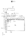
図11は本発明の液晶表示装置を構成する液晶表示パネルの構成を説明する模式図である。ここでは、所謂TN方式の液晶表示パネルを例として説明するが、他の所謂アクティブマトリクス型についても、その画素電極構成を除いて周辺に配置される駆動回路等の構成は略同様である。図11において、液晶表示パネルPNLは薄膜トランジスタTFTに代表されるスイッチング素子を形成した第1基板SUB1とカラーフィルタを形成した第2基板SUB2とで構成される。第1基板SUB1と第2基板SUB2の間には液晶が挟持されている。
【0057】
液晶表示パネルPNLの一辺(図のx方向左側の短辺)側にはゲート駆動用の集積回路(ゲートドライバ)GDRが複数個実装され、隣接する他の辺(図のy方向上側の長辺)側にはドレイン駆動用の集積回路(ドレインドライバ)DDRが複数個実装されている。ゲートドライバGDRから液晶表示パネルPNLの表示領域にゲート線GLが敷設されている。同様にドレインドライバDDRからは液晶表示パネルPNLの表示領域にドレイン線DLがゲート線GLと交差して敷設されている。そして、隣接する2本のゲート線GLおよびドレイン線DLで囲まれた領域に各1個(2個の場合もある)の薄膜トランジスタTFTを有した1画素が形成されている。
【0058】
各ゲートドライバGDRはフレキシブルプリント基板FPC1を介して表示制御回路基板CRLPに搭載された表示制御回路CRLから走査信号を受け、複数のゲート線GLに走査信号を順次供給する。ドレインドライバDDRも同様にフレキシブルプリント基板FPC2を介して表示制御回路基板CRLPに搭載された表示制御回路CRLから画像信号を受け複数のドレインドライバDDRに画像信号を供給する。
【0059】
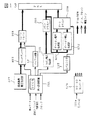
表示制御回路基板CRLPは表示信号源であるホストコンピュータHSTにケーブルCBで接続されており、各種のタイミング信号を生成するタイミングコンバータTCONや階調信号作成回路HTVC、電源回路PW、その他の表示制御信号生成回路等からなる表示制御回路CRLが搭載されている。なお、CT1,CT2,CT3はケーブルCBと表示制御回路基板CRLP、表示制御回路基板CRLPとフレキシブルプリント基板FPC1,2を接続するコネクタである。
【0060】
図12は本発明を適用する一般的なアクティブマトリクス型液晶表示装置の構成と駆動システムの説明図である。この種の液晶表示装置は、液晶表示パネルPNLと、この液晶表示パネルPNLの周辺に前記したドレイン線DL(データ線、ドレイン信号線とも言う)駆動回路(集積回路)すなわちドレインドライバDDR、走査線GL(ゲート線またはゲート信号線とも言う)駆動回路(集積回路)すなわちゲートドライバGDRを有している。これらドレインドライバDDRとゲートドライバGDRに画像表示のための表示データやクロック信号、階調電圧などを供給する表示制御手段である表示制御装置CRL、電源回路PWUを備えている。これら表示制御回路CRLは表示制御回路基板CRLPに実装されている。
【0061】
表示制御回路CRLは、コンピュータ、パソコンやテレビ受像回路などの画像信号源(図11におけるHST)からクロック信号、表示タイミング信号、同期信号などが入力される。表示制御装置CRLには、階調基準電圧生成部、タイミングントローラTCONなどが備えられており、外部からの表示データを液晶表示パネルPNLでの表示に適合した形式のデータに変換する。
【0062】
ゲートドライバGDRとドレインドライバDDRに対する表示データとクロック信号は図12に示したように供給される。ドレインドライバDDRの前段のキャリー出力は、そのまま次段のドレインドライバのキャリー入力に与えられる。
【0063】
図13は液晶表示パネルの各ドライバの概略構成と信号の流れを示すブロック図である。ドレインドライバDDRは画像信号等の表示データのデータラッチ部と出力電圧発生回路とから構成される。また、表示制御回路基板CRLPには、階調基準電圧生成部HTV、マルチプレクサMPX、コモン電圧生成部CVD、コモンドライバCDD、レベルシフト回路LST、ゲートオン電圧生成部GOV、ゲートオフ電圧生成部GFD、およびDC−DCコンバータD/Dを有する電源回路PWUが設けられる。
【0064】
図14は信号源から表示制御装置に入力される表示データおよび表示制御装置からドレインドライバとゲートドライバに出力される信号を示すタイミング図である。表示制御装置CRLは信号源からの制御信号(クロック信号、表示タイミング信号、同期信号)を受けて、ドレインドライバDDRへの制御信号としてクロックD1(所謂CL1)、シフトクロックD2(所謂CL2)および表示データを生成し、同時にゲートドライバGDRへの制御信号として、フレーム開始指示信号FLM、クロックG(所謂CL3)および表示データを生成する。
【0065】
なお、信号ソースからの表示データの伝送に低電圧差動信号(LVDS信号)を用いる方式では、当該信号ソースからのLVDS信号を上記表示制御装置を搭載する基板(インターフェイス基板)に搭載したLVDS受信回路で元の信号に変換してからゲートドライバGDRおよびドレインドライバDDRに供給する。図14に示されたように、ドレインドライバのシフト用クロック信号D2(CL2)は本体コンピュータ等から入力されるクロック信号(DCLK)および表示データの周波数と同じであり、XGA表示では約40MHz(メガヘルツ)の高周波となる。
【0066】
上記で説明した構成としたことにより、外部電極蛍光ランプの発光効率の低下を抑制して表示品質の劣化が防止される。また、本発明は、電界結合方式に限らず、電極にマイクロ波を印加するマイクロ波結合方式、あるいは磁界を印加する磁界結合方式などの各種外部電極方式の外部電極蛍光ランプにも同様に適用される。
【0067】
【発明の効果】
以上説明したように、本発明によれば、外部電極蛍光ランプの外部電極近傍における蛍光体を除去することで、その細管の内壁上の蛍光体が細管内に封入された水銀によるスパッタで消費される量を抑制される。また外部電極近傍の細管内壁にこの細管を構成するガラスよりも二次電子放出係数が大きく且つ耐スパッタ性の高い膜を形成したことにより、長寿命且つ高発光効率の外部電極蛍光ランプを備えた液晶表示装置を提供することができる。
【0068】
【図面の簡単な説明】
【図1】本発明による液晶表示装置の第1実施例の照明光源を構成する外部電極蛍光ランプの模式図である。
【図2】本発明による液晶表示装置の第2実施例の照明光源を構成する外部電極蛍光ランプの模式図である。
【図3】本発明による液晶表示装置の第3実施例の照明光源を構成する外部電極蛍光ランプの模式図である。
【図4】本発明による液晶表示装置の第4実施例の照明光源を構成する外部電極蛍光ランプの模式図である。
【図5】本発明による液晶表示装置の第5実施例の照明光源を構成する外部電極蛍光ランプの模式図である。
【図6】本発明による液晶表示装置の第6実施例の照明光源を構成する外部電極蛍光ランプの模式図である。
【図7】照明光源の1構成例である直下型バックライトの一例を説明する展開斜視図である。
【図8】本発明による液晶表示装置を実装したディスプレイモニターの一例を示す外観図である。
【図9】導光板の対向する2辺のそれぞれのサイドエッジに各1本の外部電極蛍光ランプを設置したバックライト構造体を用いた液晶表示装置の要部構造を模式的に説明する断面図である。
【図10】サイドエッジ型バックライトを備えた液晶表示装置の全体構成を説明する展開斜視図である。
【図11】本発明の液晶表示装置を構成する液晶表示パネルの構成を説明する模式図である。
【図12】本発明を適用する一般的なアクティブマトリクス型液晶表示装置の構成と駆動システムの説明図である。
【図13】液晶表示パネルの各ドライバの概略構成と信号の流れを示すブロック図である。
【図14】信号源から表示制御装置に入力される表示データおよび表示制御装置からドレインドライバとゲートドライバに出力される信号を示すタイミング図である。
【図15】電界結合方式を用いた外部電極方式の外部電極蛍光ランプの構造例を説明する模式図である。
【符号の説明】
LAMP・・・・外部電極蛍光ランプ、TB・・・・筒状細管、ED1,ED2・・・・端部電極、ED3・・・・中間電極、L1,L11,L12・・・・出光領域、L21,L22,L23・・・・端部電極領域、PH・・・・蛍光体膜、MG・・・・マグネシウム膜、HG・・・・水銀。[0001]
BACKGROUND OF THE INVENTION
The present invention relates to a liquid crystal display device, and more particularly to a liquid crystal display device including a liquid crystal display panel and an illumination light source that visualizes an electronic latent image formed on the liquid crystal display panel.
[0002]
[Prior art]
2. Description of the Related Art Liquid crystal display devices are widely used as display devices for notebook computers, display monitors, or television receivers that are capable of high definition, thinness, light weight, and color display. As a liquid crystal display panel constituting this type of liquid crystal display device, a simple matrix type using a liquid crystal display panel in which a liquid crystal layer is sandwiched between a pair of substrates having parallel electrodes formed so as to intersect each other on the inner surfaces is used. And an active matrix liquid crystal display device using a liquid crystal display panel having a switching element for selecting on a pixel basis on one of a pair of substrates.
[0003]
An active matrix liquid crystal display panel is a so-called vertical electric field method (generally referred to as a TN method) in which pixel selection electrode groups are formed on a pair of upper and lower substrates, as represented by a twisted nematic (TN) method. In addition, a so-called lateral electric field method (generally called an IPS method) in which an electrode group for pixel selection is formed on only one of a pair of upper and lower substrates is known.
[0004]
In the former TN liquid crystal display panel, the liquid crystal is twisted and oriented, for example, by 90 ° in a pair of substrates (two sheets including a first substrate (lower substrate) and a second substrate (upper substrate)). Two polarizing plates are laminated on the outer surfaces of the upper and lower substrates of the liquid crystal display panel, the absorption axis direction being arranged in a crossed Nicol manner, and the incident-side absorption axis being parallel or intersecting with the rubbing direction.
[0005]
In such a TN type active matrix liquid crystal display panel, when no voltage is applied, incident light becomes linearly polarized light on the incident side polarizing plate, and this linearly polarized light propagates along the twist of the liquid crystal layer and is transmitted through the outgoing side polarizing plate. When the axis coincides with the azimuth angle of the linearly polarized light, all the linearly polarized light is emitted and white display is performed (so-called normally open mode). When a voltage is applied, the direction of the unit vector (director) indicating the average orientation direction of the liquid crystal molecular axes constituting the liquid crystal layer is directed to the direction perpendicular to the substrate surface, and the azimuth angle of the incident side linearly polarized light is changed. Since it coincides with the absorption axis of the exit-side polarizing plate, black is displayed. (See “Basics and Applications of Liquid Crystals” published by the Industrial Research Council in 1991).
[0006]
On the other hand, a pixel selection electrode group or an electrode wiring group is formed only on one of a pair of substrates, and a liquid crystal layer is formed by applying a voltage between adjacent electrodes (between the pixel electrode and the counter electrode) on the substrate. In an IPS liquid crystal display panel that switches in a direction parallel to the surface, a polarizing plate is disposed so as to display black when no voltage is applied (so-called normally closed mode).
[0007]
In the initial state, the liquid crystal layer of the IPS liquid crystal display panel is homogeneously aligned parallel to the substrate surface, and the director of the liquid crystal layer is parallel to the substrate surface in a state parallel to the electrode wiring direction or at some angle when no voltage is applied. When the voltage is applied, the direction of the director of the liquid crystal layer shifts to a direction perpendicular to the electrode wiring direction as the voltage is applied, and the direction of the director of the liquid crystal layer is 45 compared to the direction of the director when no voltage is applied. When tilted in the direction of electrode wiring, the liquid crystal layer when the voltage is applied rotates the polarization azimuth by 90 ° like a half-wave plate, and the transmission axis of the exit side deflection plate and the polarization azimuth are Match and white display. This IPS liquid crystal display panel has a feature that a change in hue and contrast is small even at a viewing angle, and a wide viewing angle can be achieved (see Japanese Patent Application Laid-Open No. 5-505247).
[0008]
In a liquid crystal display device using the various liquid crystal display panels described above, it is necessary to provide illumination from the outside in order to visualize an electronic image (electronic latent image) formed on the liquid crystal display panel. As the illumination means, there are a passive illumination system using ambient light and an active illumination system in which a light source such as a cold cathode fluorescent lamp or a light emitting diode is installed on the back side or the front side of the liquid crystal display panel.
[0009]
Of the active illumination methods, a method (generally referred to as a front light method) in which a light source is arranged on the surface side of a liquid crystal display panel is often employed in portable information devices. On the other hand, in a liquid crystal display device having a relatively large size such as a personal computer or a display monitor, a light source is generally disposed on the back surface of the liquid crystal display panel (this is generally referred to as a backlight).
[0010]
In information devices such as notebook computers that require thinning, a linear light source such as an external electrode fluorescent lamp (hereinafter also referred to as LAMP) is arranged on the edge of a transparent plate (referred to as a light guide plate) to constitute an illumination light source. is doing. This is generally called a side edge type. However, with the recent increase in the size of the liquid crystal display panel of the liquid crystal display device used for a display monitor, a television receiver for moving pictures, etc., the screen brightness (brightness) is sufficiently obtained and the screen brightness is made uniform. Therefore, an illumination light source in which a plurality of linear light sources such as LAMP are arranged immediately below the back surface of the liquid crystal display panel is adopted. This is generally called a direct type.
[0011]
The external electrode fluorescent lamp LAMP widely used as the linear light source is a so-called low-pressure mercury lamp (fluorescent lamp), and a phosphor film is formed on the inner wall of a small-diameter cylindrical thin tube made of a transparent inorganic material such as glass or ceramics. It is configured by applying and enclosing inert gas and mercury. As means for evaporating and exciting the enclosed mercury, an internal electrode system in which at least two internal electrodes are installed in a narrow tube and a discharge is generated by applying a voltage between the electrodes is generally used.
[0012]
On the other hand, the inventors previously installed an external electrode on the outer surface of the end of the capillary tube or on the outer surface of the end and the middle, and applied an electric field to this external electrode as the excitation energy of mercury. An external electrode system was proposed (Japanese Patent Application No. 2000-162593, etc.). An example of a lamp using this method is that a pair of electrodes (so-called external electrodes) are provided apart from each other on the outer wall of a discharge tube, and an electric field generated between the electrodes is capacitively coupled to an ionized gas generated in the discharge tube. It is also called a lamp (Electric Field Coupled Discharge Lamp) or an electric field coupled electrodeless fluorescent lamp (Electric Field Coupled Electrodeless Fluorescent Discharge Lamp). The pair of electrodes are provided at both ends of the discharge tube, for example, but another external electrode is added to the outer wall of the discharge tube located between the external electrodes so as to be spaced apart from each other, and the external electrodes provided at three or more locations in the discharge tube. The electric field strength to be formed may be increased. This external electrode system does not have an electrode in a thin tube, and therefore has a feature that it has a long life because mercury is not consumed by sputtering of mercury vapor during operation. This external electrode system includes an electric field coupling system, a microwave coupling system in which a microwave is applied to the electrode, or a magnetic field coupling system in which a magnetic field is applied, depending on the means for applying energy for exciting mercury.
[0013]
FIG. 15 is a schematic diagram for explaining an example of the structure of an external electrode type fluorescent lamp using an electric field coupling method (hereinafter referred to as an external electrode fluorescent lamp). FIG. 15 (a) is an overall view, and FIG. 15 (b). Shows an enlarged cross-sectional view of the main part of FIG. In this external electrode fluorescent lamp LAMP, external electrodes ED1 and ED2 are provided on the outer periphery of both ends of a glass tubular tube TB, and a region between both external electrodes is defined as a light output region L1. The regions where the external electrodes ED1 and ED2 are installed are referred to as end electrode regions L21 and L22, respectively.
[0014]
[Problems to be solved by the invention]
A phosphor film PH is formed on the inner wall of the narrow tube TB including the end electrode regions L21 and L22 and the light output region L1 by means such as coating. A so-called three-wavelength phosphor is used as the phosphor constituting the phosphor film PH. The component is blue phosphor (Sr (CaBa) Five (PO Four ) Three Cl: Eu 2+ Or BaMg 2 Al 16 O 27 : Eu 2+ LaPO as a green phosphor Four : Ce 3+ , Tb 3+ Y as red phosphor 2 O Three : Eu 3+ Is representative. Further, mercury HG is enclosed inside the narrow tube TB.
[0015]
In this external electrode fluorescent lamp, mercury HG is consumed in the phosphor film due to the discharge during its operation. This cause is considered to be due to the combination of the metal component contained in the phosphor and mercury. The amount of mercury consumed is small compared to the amount of mercury vapor sputtered onto the electrode when the electrode is present in the narrow tube. However, in such an external electrode fluorescent lamp of the external electrode type, a blackening phenomenon occurs in the phosphor films in the regions (end electrode regions) L21 and L22 where the external electrodes are installed. This blackening phenomenon is considered to be caused by the fact that mercury vapor is sputtered on the phosphor in the external electrode region, and that much mercury is consumed, and this mercury consumption is caused by the external electrode type external electrode fluorescent lamp. This is a factor that hinders long life.
[0016]
In an internal electrode type cold cathode fluorescent lamp, the phosphor film is covered with a protective film in order to prevent a decrease in luminous efficiency due to adsorption of mercury atoms to the phosphor due to a discharge current between the electrodes in the narrow tube. Is disclosed in the Society of Illuminating Engineers Research Materials (January 2000, MD-00-34). However, in this document, the deterioration of the phosphor film between the internal electrodes is a problem, and no consideration is given to the installation area of the external electrode and the consumption of mercury in the external electrode type fluorescent lamp. Absent.
[0017]
An object of the present invention is to provide a liquid crystal display device that further suppresses mercury consumption in an external electrode type external electrode fluorescent lamp used as an illumination light source and further extends its life.
[0018]
In order to achieve the above object, the present invention removes the phosphor film in the vicinity of the external electrode where sputtering of the enclosed mercury is most likely to occur in a liquid crystal display device using an external electrode type fluorescent lamp as an illumination light source. It is characterized by that. Further, the present invention is characterized in that a film having a higher secondary electron emission coefficient and higher sputtering resistance is formed in the external electrode installation region than the glass constituting the thin tube. Further, the phosphor film in the external electrode installation region is covered with a film having a higher secondary electron emission coefficient than glass and high sputtering resistance. Hereinafter, representative configurations of the present invention will be described.
[0019]
(1) A liquid crystal display device comprising a liquid crystal display panel and an illumination light source that is installed in the liquid crystal display panel and visualizes an electronic latent image formed on the liquid crystal display panel,
The illuminating light source is a phosphor film that is formed only on the inner wall of the light emission region of a cylindrical tubule having an outer electrode in each of the end electrode regions on the outer surface and having a light emission region between the end electrode regions. And an external electrode fluorescent lamp in which mercury is sealed inside the cylindrical tubule.
[0020]
(2) A liquid crystal display device comprising a liquid crystal display panel and an illumination light source that is installed in the liquid crystal display panel and visualizes an electronic latent image formed on the liquid crystal display panel,
The illumination light source includes an external electrode at least in each end electrode region on the outer surface, and has a light output region between the end electrode regions, and the light output region and each end electrode region of the cylindrical tubule A phosphor film formed on the inner wall including the end electrode region, covering the phosphor film of each end electrode region, the inner wall of the end electrode region has a high secondary electron emission coefficient, and has a sputtering resistance. An external electrode fluorescent lamp having a large material film and having mercury enclosed in the cylindrical thin tube was provided.
[0021]
(3) A liquid crystal display device comprising a liquid crystal display panel and an illumination light source that is installed in the liquid crystal display panel and visualizes an electronic latent image formed on the liquid crystal display panel,
The illumination light source includes an end electrode provided on each outer surface of each end electrode region at the end, and at least one intermediate electrode provided on an intermediate electrode region on the outer surface between the end electrodes. An external body in which a phosphor film is formed only on the inner wall of the light emission region of a cylindrical capillary having a light emission region between each end electrode region and the intermediate electrode region, and mercury is enclosed inside the cylindrical capillary An electrode fluorescent lamp was provided.
[0022]
For example, magnesium oxide is used as a sputtering resistant film having a high secondary electron emission coefficient on the inner wall of the end electrode region of the cylindrical capillary in (4) and (1) to (3). Further, an inert gas is sealed in the cylindrical tubule.
[0023]
In (5) and (1) to (4), the illumination light source installed in the liquid crystal display panel is a direct light source in which a plurality of the external electrode fluorescent lamps are arranged directly under the liquid crystal display panel.
[0024]
In (6) and (1) to (4), the illumination light source installed in the liquid crystal display panel is a side edge type light source in which the external electrode fluorescent lamp is installed along the side edge of the light guide plate.
[0025]
With each of the above-described configurations, it is possible to provide a liquid crystal display device that further suppresses mercury consumption in the external electrode type external electrode fluorescent lamp used as an illumination light source and further extends the life. The present invention is not limited to the above-described configurations and the configurations of the embodiments described later, and various modifications can be made without departing from the technical idea of the present invention.
[0026]
DETAILED DESCRIPTION OF THE INVENTION
Embodiments of the present invention will be described below in detail with reference to the drawings of the embodiments. FIG. 1 is a schematic view of an external electrode fluorescent lamp constituting an illumination light source of a first embodiment of a liquid crystal display device according to the present invention. FIG. 1A is an overall view, and FIG. 1B is an enlarged cross-sectional view of the main part of FIG. This external electrode fluorescent lamp LAMP is provided with end electrodes ED1 and ED2 on the outer periphery of both end portions of a glass tubular tube TB. A region L1 between both end electrodes ED1 and ED2 is a light emission region, and a region provided with both end electrodes ED1 and ED2 is end electrode regions L21 and L22, respectively.
[0027]
In FIG. 1, end electrodes ED1 and ED2 are installed on the outer periphery of end electrode regions L21 and L22 at both ends of the narrow tube TB, respectively. The phosphor film PH is formed only in the light output region L1 that avoids the end electrode regions L21 and L22 on the inner wall. In addition, although inert gas, such as neon, argon, and helium, is enclosed inside the thin tube TB, this gas is not essential. FIG. 1B shows an enlarged sectional view of the end electrode region L21.
[0028]
The electric field generated by the end electrodes ED1 and ED2 is concentrated in the vicinity of the inner walls of the end electrode regions L21 and L22 provided with the end electrodes ED1 and ED2, and evaporated mercury vapor is likely to collect. When this portion of the phosphor film is present, mercury reacts with a substance constituting the phosphor to produce a compound. As a result, the above-described mercury consumption occurs. However, as in the present embodiment, since no phosphor film is present on the inner walls of the end electrode regions L21 and L22, the consumption of mercury is suppressed. As described above, according to this embodiment, the consumption of mercury enclosed in the thin tube of the external electrode fluorescent lamp LAMP is reduced, and the life is extended.
[0029]
FIG. 2 is a schematic view of an external electrode fluorescent lamp constituting the illumination light source of the second embodiment of the liquid crystal display device according to the present invention. FIG. 1A is an overall view, and FIG. 1B is an enlarged cross-sectional view of the main part of FIG. This external electrode fluorescent lamp LAMP is provided with end electrodes ED1 and ED2 on the outer periphery of both end portions of a glass tubular tube TB. A region L1 between both end electrodes ED1 and ED2 is a light emission region, and a region provided with both end electrodes ED1 and ED2 is end electrode regions L21 and L22, respectively.
[0030]
In FIG. 2, end electrodes ED1 and ED2 are installed on the outer periphery of the end electrode regions L21 and L22 at both ends of the thin tube TB, respectively. The phosphor film PH is formed only in the light output region L1 that avoids the end electrode regions L21 and L22 on the inner wall. In the end electrode regions L21 and L22, a magnesium oxide film MG having a higher secondary electron emission coefficient and higher sputtering resistance than the glass constituting the thin tube TB is formed. In addition, although inert gas, such as neon, argon, and helium, is enclosed inside the thin tube TB, this gas is not essential. FIG. 2B shows an enlarged sectional view of the end electrode region L21.
[0031]
The electric field generated by the end electrodes ED1 and ED2 is concentrated in the vicinity of the inner walls of the end electrode regions L21 and L22 provided with the end electrodes ED1 and ED2, and evaporated mercury vapor is likely to collect. When this portion of the phosphor film is present, mercury reacts with a substance constituting the phosphor to produce a compound. As a result, the above-described mercury consumption occurs. However, as in this embodiment, since no phosphor film is present on the inner walls of the end electrode regions L21 and L22, mercury is not consumed in this portion.
[0032]
Further, since the magnesium oxide film MG is formed on the inner walls of the end electrode regions L21 and L22 where the phosphor film is not formed, the primary electrons from the mercury atoms collide with the magnesium oxide film MG and secondary electrons are emitted. This becomes the excitation energy of the phosphor film together with the primary electrons, thereby increasing the amount of ultraviolet rays generated. As a result, the emission luminance of the external electrode fluorescent lamp LAMP is increased. As described above, according to this embodiment, the consumption of mercury enclosed in the thin tube of the external electrode fluorescent lamp LAMP is reduced, the life is extended, and the discharge efficiency in the tube is also improved.
[0033]
FIG. 3 is a schematic view of an external electrode fluorescent lamp constituting the illumination light source of the third embodiment of the liquid crystal display device according to the present invention. FIG. 1A is an overall view, and FIG. 1B is an enlarged cross-sectional view of the main part of FIG. This external electrode fluorescent lamp LAMP is provided with end electrodes ED1 and ED2 on the outer circumferences of both ends of a glass tubular tube TB. A region L1 between both end electrodes ED1 and ED2 is a light emission region, and a region provided with both end electrodes ED1 and ED2 is end electrode regions L21 and L22, respectively.
[0034]
In FIG. 3, end electrodes ED1 and ED2 are installed on the outer periphery of the end electrode regions L21 and L22 at both ends of the thin tube TB, respectively. A phosphor film PH is formed in the entire region including the end electrode regions L21 and L22 and the light output region L1 on the inner wall. A magnesium oxide film MG having a higher secondary electron emission coefficient and higher sputtering resistance than the glass constituting the thin tube TB is formed so as to cover the phosphor film PH in the end electrode regions L21 and L22. . In addition, although inert gas, such as neon, argon, and helium, is enclosed inside the thin tube TB, this gas is not essential. FIG. 2B shows an enlarged sectional view of the external electrode region L21.
[0035]
The electric field generated by the end electrodes ED1 and ED2 is concentrated in the vicinity of the inner walls of the end electrode regions L21 and L22 provided with the end electrodes ED1 and ED2, and evaporated mercury vapor is likely to collect. The substance constituting the phosphor film PH in this part reacts with mercury to generate a compound. As a result, the above-described mercury consumption occurs. However, since the phosphor film PH formed on the inner walls of the end electrode regions L21 and L22 is covered with the magnesium oxide film MG as in the present embodiment, the generation of the compound as described above is suppressed. The
[0036]
Further, the magnesium oxide film MG emits secondary electrons by collision of primary electrons from mercury atoms. This becomes the excitation energy of the phosphor film together with the primary electrons, thereby increasing the amount of ultraviolet rays generated. As a result, the emission luminance of the external electrode fluorescent lamp LAMP is increased. As described above, according to this embodiment, the consumption of mercury enclosed in the thin tube of the external electrode fluorescent lamp LAMP is reduced, and the life is extended.
[0037]
FIG. 4 is a schematic view of an external electrode fluorescent lamp constituting the illumination light source of the fourth embodiment of the liquid crystal display device according to the present invention. FIG. 1A is an overall view, and FIG. 1B is an enlarged cross-sectional view of the main part of FIG. This external electrode fluorescent lamp LAMP is provided with end electrodes ED1 and ED2 on the outer periphery of both ends of a glass tube tubule TB, and an intermediate electrode ED3 is also formed in an intermediate electrode region L23 in the middle portion of the tube tube TB. It is provided. And it has light emission area | region L11, L12 between each edge part electrode area | region L21, L22 and intermediate | middle electrode area | region L23. A phosphor film is formed only on the inner walls of the light output regions L11 and L12 of the tubular tubule TB, and mercury is sealed inside the tubular tubule. In addition, although inert gas, such as neon, argon, and helium, is enclosed inside the thin tube TB, this gas is not essential. FIG. 4B shows an enlarged sectional view of the end electrode region L21 and the intermediate electrode region L23.
[0038]
Electric fields generated by the external electrodes ED1, ED2, ED3 are concentrated in the vicinity of the inner walls of the end electrode regions L21, L22 provided with the end electrodes ED1, ED2 and the intermediate electrode region L23 provided with the intermediate electrode ED3. Mercury vapor is easy to collect. When a phosphor film is present in this portion, mercury reacts with a substance constituting the phosphor to produce a compound. As a result, the above-described mercury consumption occurs. However, as in the present embodiment, since no phosphor film is present on the inner walls of the end electrode regions L21 and L22 and the intermediate protruding region L23, the consumption of mercury is suppressed. As described above, according to this embodiment, the consumption of mercury enclosed in the thin tube of the external electrode fluorescent lamp LAMP is reduced, and the life is extended.
[0039]
FIG. 5 is a schematic view of an external electrode fluorescent lamp constituting the illumination light source of the fifth embodiment of the liquid crystal display device according to the present invention. FIG. 1A is an overall view, and FIG. 1B is an enlarged cross-sectional view of the main part of FIG. This external electrode fluorescent lamp LAMP is provided with end electrodes ED1 and ED2 on the outer periphery of both ends of a glass tubular tube TB, and an intermediate electrode ED3 on the outer periphery of the central portion. The regions L11 and L12 between the end electrodes ED1 and ED2 and the intermediate electrode ED3 are light emission regions, and the regions where the end electrodes ED1 and ED2 and the intermediate electrode ED3 are provided are the end electrode regions L21 and L22 and the intermediate electrode region L23, respectively. is there.
[0040]
In FIG. 5, end electrodes ED1 and ED2 are installed on the outer periphery of the end electrode regions L21 and L22 at both ends of the narrow tube TB, and an intermediate electrode ED3 is installed on the outer periphery of the intermediate electrode region L23. The phosphor film PH is formed only in the light output regions L11 and L12 that avoid the end electrode regions L21 and L22 and the intermediate electrode region L23 on the inner wall. The end electrode regions L21 and L22 and the intermediate electrode region L23 are formed with a magnesium oxide film MG having a higher secondary electron emission coefficient and higher sputtering resistance than the glass constituting the thin tube TB. In addition, although inert gas, such as neon, argon, and helium, is enclosed inside the thin tube TB, this gas is not essential. FIG. 5B shows an enlarged sectional view of the end electrode region L21.
[0041]
In the vicinity of the inner walls of the end electrode regions L21 and L22 and the intermediate electrode region L23 where the end electrodes ED1 and ED2 and the intermediate electrode ED3 are installed, the electric fields generated by the end electrodes ED1 and ED2 and the intermediate electrode ED3 are concentrated. Evaporated mercury vapor is easy to collect. When this portion of the phosphor film is present, mercury reacts with a substance constituting the phosphor to produce a compound. As a result, the above-described mercury consumption occurs. However, as in this embodiment, since no phosphor film is present on the inner walls of the end electrode regions L21 and L22 and the intermediate electrode ED3, mercury is not consumed in this portion.
[0042]
Further, since the magnesium oxide film MG is formed on the inner walls of the end electrode regions L21 and L22 and the intermediate electrode electrode region L23 where the phosphor film is not formed, primary electrons from mercury atoms collide with the magnesium oxide film MG. Secondary electrons are emitted, and this becomes the excitation energy of the phosphor film together with the primary electrons, thereby increasing the amount of ultraviolet rays generated. As a result, the emission luminance of the external electrode fluorescent lamp LAMP is increased. As described above, according to this embodiment, the consumption of mercury enclosed in the thin tube of the external electrode fluorescent lamp LAMP is reduced, and the life is extended.
[0043]
FIG. 6 is a schematic view of an external electrode fluorescent lamp constituting the illumination light source of the sixth embodiment of the liquid crystal display device according to the present invention. FIG. 1A is an overall view, and FIG. 1B is an enlarged cross-sectional view of the main part of FIG. This external electrode fluorescent lamp LAMP is provided with end electrodes ED1 and ED2 on the outer periphery of both ends of a glass tube tubule TB, and an intermediate electrode ED3 on an intermediate portion. The regions L11 and L12 between the both end electrodes ED1 and ED2 and the intermediate electrode ED3 are light emission regions, the region provided with both end electrodes ED1 and ED2 and the region provided with the intermediate electrode ED3 are the end electrode regions L21 and L22 and the intermediate region, respectively. This is an electrode region.
[0044]
In FIG. 6, end electrodes ED1 and ED2 are installed on the outer periphery of the end electrode regions L21 and L22 at both ends of the narrow tube TB, and an intermediate electrode ED3 is installed on the outer periphery of the intermediate electrode region L23. A phosphor film PH is formed in the entire region including the end electrode regions L21 and L22 and the intermediate electrode region and the light output regions L1 and L2 on the inner wall. The magnesium oxide film MG that covers the phosphor film PH in the end electrode regions L21 and L22 and the intermediate electrode region L23 and has a higher secondary electron emission coefficient and higher sputtering resistance than the glass constituting the capillary tube TB. Is formed. In addition, although inert gas, such as neon, argon, and helium, is enclosed inside the narrow tube TB, this gas is not essential. FIG. 6B shows an enlarged sectional view of the external electrode region L21 and the intermediate electrode region.
[0045]
In the vicinity of the inner walls of the end electrode regions L21 and L22 where the end electrodes ED1 and ED2 are installed and in the intermediate electrode region L23 where the intermediate electrode ED3 is installed, the electric fields generated by the end electrodes ED1 and ED2 and the intermediate electrode ED3 are generated. Concentrated and evaporated mercury vapor is easy to collect. The substance constituting the phosphor film PH in this part reacts with mercury to generate a compound. As a result, the above-described mercury consumption occurs. However, since the phosphor film PH formed on the inner walls of the end electrode regions L21 and L22 and the intermediate electrode region L23 is covered with the magnesium oxide film MG as in the present embodiment, the compound as described above is used. The generation of is suppressed.
[0046]
Further, the magnesium oxide film MG emits secondary electrons by collision of primary electrons from mercury atoms. This becomes the excitation energy of the phosphor film together with the primary electrons, thereby increasing the amount of ultraviolet rays generated. As a result, the emission luminance of the external electrode fluorescent lamp LAMP is increased. As described above, according to this embodiment, the consumption of mercury enclosed in the thin tube of the external electrode fluorescent lamp LAMP is reduced, the life is extended, and the discharge efficiency in the tube is also improved.
[0047]
Next, a configuration example of an illumination light source using the external electrode fluorescent lamp described in the above embodiments, a configuration example of a liquid crystal display device incorporating this illumination light source, and a drive circuit configuration example will be described.
[0048]
FIG. 7 is an exploded perspective view illustrating an example of a direct type backlight that is one configuration example of the illumination light source. In this direct type backlight, a plurality of external electrode fluorescent lamps LAMP are arranged on the upper surface of a lower frame FLM-D generally made of a metal material so that their longitudinal directions are parallel to each other. The upper frame FLM-U is put on this, and both are united with the claws NL. The resin frame MLD-L (left mold) and MLD-R (right mold) are used on both sides (left and right). The lower frame FLM-D is sandwiched and integrated.
[0049]
In FIG. 7, the surface of the lower frame FLM-D on the external electrode fluorescent lamp LAMP side has a function of a reflector. However, although not shown in the drawing, another member such as a sheet having a light reflecting function is inserted between the lower frame FLM-D and the external electrode fluorescent lamp LAMP, or the longitudinal direction of the external electrode fluorescent lamp LAMP is lowered. There is a type in which a chevron-shaped reflector is disposed on the entire surface of the frame FLM-D, and a chevron-shaped reflector is disposed in a portion excluding the lower part of the LAMP of the reflective sheet or the lower frame FLM-D having a reflective function.
[0050]
Then, an optical compensation sheet OPS composed of a light diffusing plate SCT (hereinafter simply referred to as a diffusing plate), a diffusing sheet SCTS, a prism sheet PRS and the like is laminated on the upper frame FLM-U to constitute a direct type backlight. ing. Some have only one of the diffusion plate SCT and the diffusion sheet SCTS. A liquid crystal display panel (not shown) is placed above the direct type backlight, and a power source for driving the external electrode fluorescent lamp LAMP, other necessary circuits, and structural members are mounted. The direct type backlight is not limited to the above configuration, and various assembled shapes are known.
[0051]
FIG. 8 is an external view showing an example of a display monitor in which the liquid crystal display device according to the present invention is mounted. The backlight constituting the liquid crystal display device mounted on the screen of the monitor, that is, the display unit is a direct type backlight using the external electrode fluorescent lamp described in any of the above embodiments. In the figure, PNL is a display surface of a liquid crystal display panel constituting the liquid crystal display device.
[0052]
FIG. 9 is a cross-sectional view schematically illustrating the main structure of a liquid crystal display device using a backlight structure in which one external electrode fluorescent lamp is installed on each of the two opposing side edges of the light guide plate. is there. In the figure, reference numeral BL denotes a backlight structure, and one external electrode fluorescent lamp LAMP1, LAMP2 is arranged along each of two opposing sides of a flat light guide plate GLB preferably made of acrylic resin. ing. Any of the above embodiments is used for each external electrode fluorescent lamp. Lamp reflecting sheets LS1 and LS2 are installed on the portion of the external electrode fluorescent lamps LAMP1 and LAMP2 excluding the portion facing the light guide body GLB, and the back surface of the light guide plate GLB is provided with a reflector plate RF.
[0053]
A diffusion plate SPS and a prism sheet PRS are stacked on the upper surface of the light guide plate GLB, and a liquid crystal display panel PNL is stacked on the diffusion plate SPS and the prism sheet PRS. The liquid crystal display panel PNL is formed by sealing a liquid crystal layer between a pair of substrates SUB1 and SUB2, and polarizing plates POL1 and POL2 are provided on both surfaces.
[0054]
FIG. 10 is a developed perspective view illustrating the entire configuration of a liquid crystal display device having a side edge type backlight. The liquid crystal display device includes a liquid crystal display panel PNL, a light guide plate GLB, external electrode fluorescent lamps LAMP1, LAMP2, a lower case MCA containing an optical sheet composed of a diffusion plate SPS and a prism sheet PRS, and a frame-like member. The case SHD is covered with the lower case MCA, and the claws NL around the upper case SHD are crimped and integrated with the engaging portion NA of the lower case MCA. This engagement is performed by bending the claw NL inside the engagement portion NA.
[0055]
The liquid crystal display device according to the present invention is not limited to a display monitor or a notebook computer, but can be used for a display device of a television receiver or other devices.
[0056]
FIG. 11 is a schematic diagram for explaining a configuration of a liquid crystal display panel constituting the liquid crystal display device of the present invention. Here, a so-called TN liquid crystal display panel will be described as an example, but other so-called active matrix types have substantially the same configuration of drive circuits and the like arranged in the periphery except for the pixel electrode configuration. In FIG. 11, the liquid crystal display panel PNL includes a first substrate SUB1 on which a switching element represented by a thin film transistor TFT is formed, and a second substrate SUB2 on which a color filter is formed. Liquid crystal is sandwiched between the first substrate SUB1 and the second substrate SUB2.
[0057]
A plurality of integrated circuits (gate drivers) GDR for driving a gate are mounted on one side of the liquid crystal display panel PNL (the short side on the left side in the x direction in the figure), and another adjacent side (the long side on the upper side in the y direction in the figure). ) Side, a plurality of integrated circuits (drain drivers) DDR for driving the drain are mounted. A gate line GL is laid from the gate driver GDR to the display area of the liquid crystal display panel PNL. Similarly, a drain line DL is laid from the drain driver DDR across the gate line GL in the display area of the liquid crystal display panel PNL. One pixel having one (or two in some cases) thin film transistor TFT is formed in a region surrounded by two adjacent gate lines GL and drain lines DL.
[0058]
Each gate driver GDR receives a scanning signal from the display control circuit CRL mounted on the display control circuit board CRLP via the flexible printed circuit board FPC1, and sequentially supplies the scanning signal to the plurality of gate lines GL. Similarly, the drain driver DDR receives an image signal from the display control circuit CRL mounted on the display control circuit board CRLP via the flexible printed circuit board FPC2, and supplies the image signal to the plurality of drain drivers DDR.
[0059]
The display control circuit board CRLP is connected to a host computer HST, which is a display signal source, by a cable CB. The timing converter TCON that generates various timing signals, the gradation signal generation circuit HTVC, the power supply circuit PW, and other display control signals A display control circuit CRL including a generation circuit and the like is mounted. CT1, CT2 and CT3 are connectors for connecting the cable CB and the display control circuit board CRLP, and the display control circuit board CRLP and the flexible printed circuit boards FPC1 and FPC2.
[0060]
FIG. 12 is an explanatory diagram of a configuration and driving system of a general active matrix type liquid crystal display device to which the present invention is applied. This type of liquid crystal display device includes a liquid crystal display panel PNL and a drain line DL (also referred to as a data line or a drain signal line) driving circuit (integrated circuit), that is, a drain driver DDR, a scanning line around the liquid crystal display panel PNL. A GL (also referred to as a gate line or a gate signal line) driving circuit (integrated circuit), that is, a gate driver GDR is included. The drain driver DDR and the gate driver GDR are provided with a display control device CRL which is a display control means for supplying display data, a clock signal, a gradation voltage and the like for image display, and a power supply circuit PWU. These display control circuits CRL are mounted on a display control circuit board CRLP.
[0061]
The display control circuit CRL receives a clock signal, a display timing signal, a synchronization signal, and the like from an image signal source (HST in FIG. 11) such as a computer, a personal computer, or a television receiver circuit. The display control device CRL includes a gradation reference voltage generation unit, a timing controller TCON, and the like, and converts display data from the outside into data in a format suitable for display on the liquid crystal display panel PNL.
[0062]
Display data and clock signals for the gate driver GDR and the drain driver DDR are supplied as shown in FIG. The carry output of the previous stage of the drain driver DDR is directly supplied to the carry input of the drain driver of the next stage.
[0063]
FIG. 13 is a block diagram showing a schematic configuration and a signal flow of each driver of the liquid crystal display panel. The drain driver DDR includes a data latch unit for display data such as an image signal and an output voltage generation circuit. The display control circuit board CRLP includes a gradation reference voltage generation unit HTV, a multiplexer MPX, a common voltage generation unit CVD, a common driver CDD, a level shift circuit LST, a gate-on voltage generation unit GOV, a gate-off voltage generation unit GFD, and a DC. A power supply circuit PWU having a DC converter D / D is provided.
[0064]
FIG. 14 is a timing chart showing display data input from the signal source to the display control device and signals output from the display control device to the drain driver and the gate driver. The display control device CRL receives control signals (clock signal, display timing signal, synchronization signal) from the signal source, and controls the clock D1 (so-called CL1), the shift clock D2 (so-called CL2) and the display as control signals to the drain driver DDR. At the same time, a frame start instruction signal FLM, a clock G (so-called CL3), and display data are generated as control signals to the gate driver GDR.
[0065]
In the method using a low-voltage differential signal (LVDS signal) for transmission of display data from a signal source, LVDS reception in which the LVDS signal from the signal source is mounted on a substrate (interface substrate) on which the display control device is mounted. After being converted into the original signal by the circuit, it is supplied to the gate driver GDR and the drain driver DDR. As shown in FIG. 14, the clock signal D2 (CL2) for shifting the drain driver is the same as the frequency of the clock signal (DCLK) and display data input from the main body computer or the like, and about 40 MHz (megahertz) in the XGA display. ).
[0066]
With the configuration described above, it is possible to prevent deterioration in display quality by suppressing a decrease in the luminous efficiency of the external electrode fluorescent lamp. The present invention is not limited to the electric field coupling method, and is similarly applied to external electrode fluorescent lamps of various external electrode methods such as a microwave coupling method in which a microwave is applied to an electrode or a magnetic field coupling method in which a magnetic field is applied. The
[0067]
【The invention's effect】
As described above, according to the present invention, by removing the phosphor in the vicinity of the external electrode of the external electrode fluorescent lamp, the phosphor on the inner wall of the thin tube is consumed by sputtering with mercury enclosed in the thin tube. The amount to be suppressed is suppressed. In addition, an external electrode fluorescent lamp with a long life and high luminous efficiency is provided by forming a film having a higher secondary electron emission coefficient and higher sputtering resistance than the glass constituting the thin tube on the inner wall of the thin tube near the external electrode. A liquid crystal display device can be provided.
[0068]
[Brief description of the drawings]
FIG. 1 is a schematic view of an external electrode fluorescent lamp constituting an illumination light source of a first embodiment of a liquid crystal display device according to the present invention.
FIG. 2 is a schematic view of an external electrode fluorescent lamp constituting an illumination light source of a second embodiment of the liquid crystal display device according to the present invention.
FIG. 3 is a schematic diagram of an external electrode fluorescent lamp constituting an illumination light source of a third embodiment of the liquid crystal display device according to the present invention.
FIG. 4 is a schematic view of an external electrode fluorescent lamp constituting an illumination light source of a fourth embodiment of the liquid crystal display device according to the present invention.
FIG. 5 is a schematic view of an external electrode fluorescent lamp constituting an illumination light source of a fifth embodiment of the liquid crystal display device according to the present invention.
FIG. 6 is a schematic view of an external electrode fluorescent lamp constituting an illumination light source of a sixth embodiment of the liquid crystal display device according to the present invention.
FIG. 7 is an exploded perspective view illustrating an example of a direct type backlight that is one configuration example of an illumination light source.
FIG. 8 is an external view showing an example of a display monitor on which the liquid crystal display device according to the present invention is mounted.
FIG. 9 is a cross-sectional view schematically illustrating a main part structure of a liquid crystal display device using a backlight structure in which one external electrode fluorescent lamp is installed on each of two opposing sides of a light guide plate. It is.
FIG. 10 is an exploded perspective view illustrating the entire configuration of a liquid crystal display device including a side edge type backlight.
FIG. 11 is a schematic diagram illustrating a configuration of a liquid crystal display panel included in the liquid crystal display device of the present invention.
FIG. 12 is an explanatory diagram of a configuration and driving system of a general active matrix liquid crystal display device to which the present invention is applied.
FIG. 13 is a block diagram showing a schematic configuration and a signal flow of each driver of the liquid crystal display panel.
FIG. 14 is a timing chart showing display data input from the signal source to the display control device and signals output from the display control device to the drain driver and the gate driver.
FIG. 15 is a schematic diagram illustrating an example of the structure of an external electrode fluorescent lamp using an external electrode method using an electric field coupling method.
[Explanation of symbols]
LAMP ... external electrode fluorescent lamp, TB ... cylindrical tube, ED1, ED2, ... end electrode, ED3 ... intermediate electrode, L1, L11, L12 ... light emission area, L21, L22, L23... End electrode region, PH... Phosphor film, MG... Magnesium film, HG.
Claims (13)
前記照明光源は、
少なくとも外面の各端部電極領域のそれぞれに外部電極を備え、前記端部電極領域の間に出光領域を有する筒状細管を有しており、
前記筒状細管は、前記外部電極の配置位置とは重畳しない前記出光領域の内壁にのみに蛍光体膜を有し、前記筒状細管の内部に水銀を封入した外部電極蛍光ランプである液晶表示装置。A liquid crystal display device comprising a liquid crystal display panel and an illumination light source that is installed in the liquid crystal display panel and visualizes an electronic latent image formed on the liquid crystal display panel,
The illumination light source is
Comprising a respective external electrodes of each end electrode area of at least the outer surface has a cylindrical capillary having a light exit region between the front Kitan unit electrode area,
It said tubular capillaries, the position of the external electrode has a Minihotaru light film of the inner wall of the light exit region which does not overlap, are external electrode fluorescent lamp filled with mercury to the inside of the cylindrical capillary liquid crystal display device.
前記照明光源は、筒状細管の外面の各端部に外部電極を有した外部電極蛍光ランプを備えて構成されており、
該外部電極蛍光ランプは、前記筒状細管の内面の各外部電極間に、該外部電極と重畳しないように蛍光体膜が配置されていることを特徴とする液晶表示装置。A liquid crystal display device comprising a liquid crystal display panel and an illumination light source,
The illumination light source comprises an external electrode fluorescent lamp having an external electrode at each end of the outer surface of the cylindrical tubule,
External electrode fluorescent lamp, between the outer electrodes of the inner surface of the cylindrical narrow tube, a liquid crystal display device comprising the phosphor film so as not to overlap with the external electrodes are arranged.
Priority Applications (1)
| Application Number | Priority Date | Filing Date | Title |
|---|---|---|---|
| JP2001283500A JP4050886B2 (en) | 2001-09-18 | 2001-09-18 | Liquid crystal display |
Applications Claiming Priority (1)
| Application Number | Priority Date | Filing Date | Title |
|---|---|---|---|
| JP2001283500A JP4050886B2 (en) | 2001-09-18 | 2001-09-18 | Liquid crystal display |
Related Child Applications (1)
| Application Number | Title | Priority Date | Filing Date |
|---|---|---|---|
| JP2005091528A Division JP2005301263A (en) | 2005-03-28 | 2005-03-28 | Liquid crystal display device |
Publications (3)
| Publication Number | Publication Date |
|---|---|
| JP2003091007A JP2003091007A (en) | 2003-03-28 |
| JP2003091007A5 JP2003091007A5 (en) | 2005-09-15 |
| JP4050886B2 true JP4050886B2 (en) | 2008-02-20 |
Family
ID=19106979
Family Applications (1)
| Application Number | Title | Priority Date | Filing Date |
|---|---|---|---|
| JP2001283500A Expired - Fee Related JP4050886B2 (en) | 2001-09-18 | 2001-09-18 | Liquid crystal display |
Country Status (1)
| Country | Link |
|---|---|
| JP (1) | JP4050886B2 (en) |
Families Citing this family (11)
| Publication number | Priority date | Publication date | Assignee | Title |
|---|---|---|---|---|
| WO2005071714A1 (en) * | 2004-01-22 | 2005-08-04 | Matsushita Electric Industrial Co., Ltd. | External-electrode discharge lamp, external-electrode discharge lamp manufacturing method, and backlight unit |
| DE102004006614A1 (en) * | 2004-02-10 | 2005-08-25 | Patent-Treuhand-Gesellschaft für elektrische Glühlampen mbH | lighting device |
| KR100705095B1 (en) | 2004-03-05 | 2007-04-06 | 닛본 덴끼 가부시끼가이샤 | External electrode type discharge lamp and method of manufacturing the same |
| KR101078479B1 (en) | 2004-12-30 | 2011-10-31 | 엘지디스플레이 주식회사 | Lamp for back light |
| TW200705510A (en) | 2005-05-13 | 2007-02-01 | Matsushita Electric Ind Co Ltd | Fluorescent lamp, backlight unit, and liquid crystal display device |
| US20080252193A1 (en) | 2005-05-31 | 2008-10-16 | Kenji Yamada | Fluorescent Lamp, Backlight Unit and Liquid Crystal Television |
| JP2007018737A (en) * | 2005-07-05 | 2007-01-25 | Matsushita Electric Ind Co Ltd | Fluorescent lamp and backlight device |
| JP2007073481A (en) * | 2005-09-09 | 2007-03-22 | Nec Lighting Ltd | Discharge lamp |
| KR100706184B1 (en) * | 2005-12-26 | 2007-04-12 | 주식회사 디엠에스 | Fluorescent lamp and manufacturing method thereof |
| KR100795832B1 (en) | 2005-12-26 | 2008-01-17 | 주식회사 디엠에스 | Composition for forming of layer, fluorescent lamp thereby and manufacturing method thereof |
| KR101183418B1 (en) * | 2005-12-30 | 2012-09-14 | 엘지디스플레이 주식회사 | External Electrode Florescent Lamp And Backlight Unit Of Liquid Crtstal Display Device |
-
2001
- 2001-09-18 JP JP2001283500A patent/JP4050886B2/en not_active Expired - Fee Related
Also Published As
| Publication number | Publication date |
|---|---|
| JP2003091007A (en) | 2003-03-28 |
Similar Documents
| Publication | Publication Date | Title |
|---|---|---|
| US7527406B2 (en) | Backlight assembly and liquid crystal display device with reduced noise | |
| US7286193B2 (en) | Liquid crystal display unit having a field sequential driven backlight unit | |
| US20060002143A1 (en) | Backlight unit of liquid crystal display device using light emitting diode and method of driving the same | |
| JP4050886B2 (en) | Liquid crystal display | |
| US20080002112A1 (en) | Liquid crystal display device and fabrication method thereof | |
| US20070108917A1 (en) | Inverter circuit, backlight and liquid crystal display | |
| US7999784B2 (en) | Backlight unit of liquid crystal display device and method for driving the same | |
| WO2004090619A1 (en) | Liquid crystal display apparatus | |
| US20070263136A1 (en) | Backlight unit and liquid crystal display device having the same | |
| JP2003107463A (en) | Liquid crystal display device | |
| US8054009B2 (en) | Lamp driving device and liquid crystal display device having the same | |
| US20060262560A1 (en) | Flat fluorescent lamp and display device provided with the same | |
| JP2005301263A (en) | Liquid crystal display device | |
| US7808190B2 (en) | Display apparatus and power supplying apparatus for lamp unit thereof | |
| KR20050060232A (en) | Apparatus driving lamp of liquid crystal display device | |
| US7350935B2 (en) | Backlight assembly | |
| JP2000305080A (en) | Illuminating light source integrated type liquid crystal display device | |
| KR101235700B1 (en) | Transformer and backlight drive part for liquid crystal display device including the same | |
| JP4809751B2 (en) | Liquid crystal display | |
| US7868551B2 (en) | Fluorescent tube having an increasing internal diameter, a method of driving the fluorescent tube, an illuminating device for display device, and a display device having the illuminating device | |
| KR100971391B1 (en) | Liquid crystal display device | |
| KR101222981B1 (en) | Circuit for driving of Liquid Crystal Display Device | |
| KR101002345B1 (en) | The back light of the liquid crystal display device | |
| JP2007035462A (en) | Flat light source and display device using the same | |
| KR20050019194A (en) | Back light assembly and liquid crystal display having the same |
Legal Events
| Date | Code | Title | Description |
|---|---|---|---|
| A521 | Written amendment |
Free format text: JAPANESE INTERMEDIATE CODE: A523 Effective date: 20050328 |
|
| A621 | Written request for application examination |
Free format text: JAPANESE INTERMEDIATE CODE: A621 Effective date: 20050328 |
|
| A977 | Report on retrieval |
Free format text: JAPANESE INTERMEDIATE CODE: A971007 Effective date: 20070719 |
|
| A131 | Notification of reasons for refusal |
Free format text: JAPANESE INTERMEDIATE CODE: A131 Effective date: 20070814 |
|
| A521 | Written amendment |
Free format text: JAPANESE INTERMEDIATE CODE: A523 Effective date: 20071011 |
|
| TRDD | Decision of grant or rejection written | ||
| A01 | Written decision to grant a patent or to grant a registration (utility model) |
Free format text: JAPANESE INTERMEDIATE CODE: A01 Effective date: 20071127 |
|
| A61 | First payment of annual fees (during grant procedure) |
Free format text: JAPANESE INTERMEDIATE CODE: A61 Effective date: 20071130 |
|
| R150 | Certificate of patent or registration of utility model |
Free format text: JAPANESE INTERMEDIATE CODE: R150 |
|
| FPAY | Renewal fee payment (event date is renewal date of database) |
Free format text: PAYMENT UNTIL: 20101207 Year of fee payment: 3 |
|
| FPAY | Renewal fee payment (event date is renewal date of database) |
Free format text: PAYMENT UNTIL: 20101207 Year of fee payment: 3 |
|
| S531 | Written request for registration of change of domicile |
Free format text: JAPANESE INTERMEDIATE CODE: R313531 |
|
| R371 | Transfer withdrawn |
Free format text: JAPANESE INTERMEDIATE CODE: R371 |
|
| FPAY | Renewal fee payment (event date is renewal date of database) |
Free format text: PAYMENT UNTIL: 20101207 Year of fee payment: 3 |
|
| FPAY | Renewal fee payment (event date is renewal date of database) |
Free format text: PAYMENT UNTIL: 20111207 Year of fee payment: 4 |
|
| FPAY | Renewal fee payment (event date is renewal date of database) |
Free format text: PAYMENT UNTIL: 20111207 Year of fee payment: 4 |
|
| S111 | Request for change of ownership or part of ownership |
Free format text: JAPANESE INTERMEDIATE CODE: R313115 |
|
| S631 | Written request for registration of reclamation of domicile |
Free format text: JAPANESE INTERMEDIATE CODE: R313631 |
|
| R350 | Written notification of registration of transfer |
Free format text: JAPANESE INTERMEDIATE CODE: R350 |
|
| FPAY | Renewal fee payment (event date is renewal date of database) |
Free format text: PAYMENT UNTIL: 20111207 Year of fee payment: 4 |
|
| S111 | Request for change of ownership or part of ownership |
Free format text: JAPANESE INTERMEDIATE CODE: R313117 |
|
| FPAY | Renewal fee payment (event date is renewal date of database) |
Free format text: PAYMENT UNTIL: 20111207 Year of fee payment: 4 |
|
| R350 | Written notification of registration of transfer |
Free format text: JAPANESE INTERMEDIATE CODE: R350 |
|
| FPAY | Renewal fee payment (event date is renewal date of database) |
Free format text: PAYMENT UNTIL: 20111207 Year of fee payment: 4 |
|
| S111 | Request for change of ownership or part of ownership |
Free format text: JAPANESE INTERMEDIATE CODE: R313121 Free format text: JAPANESE INTERMEDIATE CODE: R313115 |
|
| FPAY | Renewal fee payment (event date is renewal date of database) |
Free format text: PAYMENT UNTIL: 20111207 Year of fee payment: 4 |
|
| R350 | Written notification of registration of transfer |
Free format text: JAPANESE INTERMEDIATE CODE: R350 |
|
| FPAY | Renewal fee payment (event date is renewal date of database) |
Free format text: PAYMENT UNTIL: 20111207 Year of fee payment: 4 |
|
| FPAY | Renewal fee payment (event date is renewal date of database) |
Free format text: PAYMENT UNTIL: 20121207 Year of fee payment: 5 |
|
| FPAY | Renewal fee payment (event date is renewal date of database) |
Free format text: PAYMENT UNTIL: 20121207 Year of fee payment: 5 |
|
| FPAY | Renewal fee payment (event date is renewal date of database) |
Free format text: PAYMENT UNTIL: 20131207 Year of fee payment: 6 |
|
| LAPS | Cancellation because of no payment of annual fees |