JP4040780B2 - Recording timing setting system and information recording system - Google Patents
Recording timing setting system and information recording system Download PDFInfo
- Publication number
- JP4040780B2 JP4040780B2 JP37441498A JP37441498A JP4040780B2 JP 4040780 B2 JP4040780 B2 JP 4040780B2 JP 37441498 A JP37441498 A JP 37441498A JP 37441498 A JP37441498 A JP 37441498A JP 4040780 B2 JP4040780 B2 JP 4040780B2
- Authority
- JP
- Japan
- Prior art keywords
- signal
- recording
- timing
- information
- sync
- Prior art date
- Legal status (The legal status is an assumption and is not a legal conclusion. Google has not performed a legal analysis and makes no representation as to the accuracy of the status listed.)
- Expired - Fee Related
Links
- 238000001514 detection method Methods 0.000 claims description 86
- 238000000034 method Methods 0.000 description 40
- 238000010586 diagram Methods 0.000 description 20
- 230000000630 rising effect Effects 0.000 description 10
- 230000003287 optical effect Effects 0.000 description 5
- 201000009310 astigmatism Diseases 0.000 description 4
- 239000010408 film Substances 0.000 description 3
- PCHJSUWPFVWCPO-UHFFFAOYSA-N gold Chemical compound [Au] PCHJSUWPFVWCPO-UHFFFAOYSA-N 0.000 description 3
- 239000010931 gold Substances 0.000 description 3
- 229910052737 gold Inorganic materials 0.000 description 3
- 238000007740 vapor deposition Methods 0.000 description 3
- 230000001681 protective effect Effects 0.000 description 2
- 239000011347 resin Substances 0.000 description 2
- 229920005989 resin Polymers 0.000 description 2
- 239000000758 substrate Substances 0.000 description 2
- 230000001360 synchronised effect Effects 0.000 description 2
- 238000012935 Averaging Methods 0.000 description 1
- 230000015572 biosynthetic process Effects 0.000 description 1
- 238000006243 chemical reaction Methods 0.000 description 1
- 239000000284 extract Substances 0.000 description 1
- 230000007274 generation of a signal involved in cell-cell signaling Effects 0.000 description 1
- 230000010355 oscillation Effects 0.000 description 1
- 230000000717 retained effect Effects 0.000 description 1
- 238000009751 slip forming Methods 0.000 description 1
- 239000010409 thin film Substances 0.000 description 1
- 230000007704 transition Effects 0.000 description 1
Images
Classifications
-
- G—PHYSICS
- G11—INFORMATION STORAGE
- G11B—INFORMATION STORAGE BASED ON RELATIVE MOVEMENT BETWEEN RECORD CARRIER AND TRANSDUCER
- G11B27/00—Editing; Indexing; Addressing; Timing or synchronising; Monitoring; Measuring tape travel
- G11B27/10—Indexing; Addressing; Timing or synchronising; Measuring tape travel
- G11B27/19—Indexing; Addressing; Timing or synchronising; Measuring tape travel by using information detectable on the record carrier
- G11B27/24—Indexing; Addressing; Timing or synchronising; Measuring tape travel by using information detectable on the record carrier by sensing features on the record carrier other than the transducing track ; sensing signals or marks recorded by another method than the main recording
-
- G—PHYSICS
- G11—INFORMATION STORAGE
- G11B—INFORMATION STORAGE BASED ON RELATIVE MOVEMENT BETWEEN RECORD CARRIER AND TRANSDUCER
- G11B20/00—Signal processing not specific to the method of recording or reproducing; Circuits therefor
- G11B20/10—Digital recording or reproducing
-
- G—PHYSICS
- G11—INFORMATION STORAGE
- G11B—INFORMATION STORAGE BASED ON RELATIVE MOVEMENT BETWEEN RECORD CARRIER AND TRANSDUCER
- G11B20/00—Signal processing not specific to the method of recording or reproducing; Circuits therefor
- G11B20/10—Digital recording or reproducing
- G11B20/14—Digital recording or reproducing using self-clocking codes
-
- G—PHYSICS
- G11—INFORMATION STORAGE
- G11B—INFORMATION STORAGE BASED ON RELATIVE MOVEMENT BETWEEN RECORD CARRIER AND TRANSDUCER
- G11B2220/00—Record carriers by type
- G11B2220/20—Disc-shaped record carriers
- G11B2220/21—Disc-shaped record carriers characterised in that the disc is of read-only, rewritable, or recordable type
- G11B2220/215—Recordable discs
- G11B2220/216—Rewritable discs
-
- G—PHYSICS
- G11—INFORMATION STORAGE
- G11B—INFORMATION STORAGE BASED ON RELATIVE MOVEMENT BETWEEN RECORD CARRIER AND TRANSDUCER
- G11B2220/00—Record carriers by type
- G11B2220/20—Disc-shaped record carriers
- G11B2220/25—Disc-shaped record carriers characterised in that the disc is based on a specific recording technology
- G11B2220/2537—Optical discs
- G11B2220/2562—DVDs [digital versatile discs]; Digital video discs; MMCDs; HDCDs
-
- G—PHYSICS
- G11—INFORMATION STORAGE
- G11B—INFORMATION STORAGE BASED ON RELATIVE MOVEMENT BETWEEN RECORD CARRIER AND TRANSDUCER
- G11B27/00—Editing; Indexing; Addressing; Timing or synchronising; Monitoring; Measuring tape travel
- G11B27/10—Indexing; Addressing; Timing or synchronising; Measuring tape travel
- G11B27/19—Indexing; Addressing; Timing or synchronising; Measuring tape travel by using information detectable on the record carrier
- G11B27/28—Indexing; Addressing; Timing or synchronising; Measuring tape travel by using information detectable on the record carrier by using information signals recorded by the same method as the main recording
- G11B27/30—Indexing; Addressing; Timing or synchronising; Measuring tape travel by using information detectable on the record carrier by using information signals recorded by the same method as the main recording on the same track as the main recording
- G11B27/3027—Indexing; Addressing; Timing or synchronising; Measuring tape travel by using information detectable on the record carrier by using information signals recorded by the same method as the main recording on the same track as the main recording used signal is digitally coded
-
- G—PHYSICS
- G11—INFORMATION STORAGE
- G11B—INFORMATION STORAGE BASED ON RELATIVE MOVEMENT BETWEEN RECORD CARRIER AND TRANSDUCER
- G11B7/00—Recording or reproducing by optical means, e.g. recording using a thermal beam of optical radiation by modifying optical properties or the physical structure, reproducing using an optical beam at lower power by sensing optical properties; Record carriers therefor
- G11B7/002—Recording, reproducing or erasing systems characterised by the shape or form of the carrier
- G11B7/0037—Recording, reproducing or erasing systems characterised by the shape or form of the carrier with discs
-
- G—PHYSICS
- G11—INFORMATION STORAGE
- G11B—INFORMATION STORAGE BASED ON RELATIVE MOVEMENT BETWEEN RECORD CARRIER AND TRANSDUCER
- G11B7/00—Recording or reproducing by optical means, e.g. recording using a thermal beam of optical radiation by modifying optical properties or the physical structure, reproducing using an optical beam at lower power by sensing optical properties; Record carriers therefor
- G11B7/004—Recording, reproducing or erasing methods; Read, write or erase circuits therefor
- G11B7/0045—Recording
-
- G—PHYSICS
- G11—INFORMATION STORAGE
- G11B—INFORMATION STORAGE BASED ON RELATIVE MOVEMENT BETWEEN RECORD CARRIER AND TRANSDUCER
- G11B7/00—Recording or reproducing by optical means, e.g. recording using a thermal beam of optical radiation by modifying optical properties or the physical structure, reproducing using an optical beam at lower power by sensing optical properties; Record carriers therefor
- G11B7/004—Recording, reproducing or erasing methods; Read, write or erase circuits therefor
- G11B7/006—Overwriting
Landscapes
- Engineering & Computer Science (AREA)
- Signal Processing (AREA)
- Optical Recording Or Reproduction (AREA)
- Signal Processing For Digital Recording And Reproducing (AREA)
- Accessory Devices And Overall Control Thereof (AREA)
Description
【0001】
【発明の属する技術分野】
本発明は、光ディスク等の記録媒体に対する記録情報の記録タイミング(記録位置)を設定して当該記録情報を記録するための記録タイミング設定装置並びに当該記録タイミング設定装置を備えた情報記録装置の技術分野に属する。
【0002】
【従来の技術】
近年、記録可能な従来の光ディスクとしてのCD−R(Compact Disk−Recordable)に比して数倍記録密度を向上させると共に記録情報を複数回記録することが可能な光ディスクであるDVD−R/Wの開発が行われているが、このDVD−R/Wに記録情報を記録するための情報記録装置においては、当該DVD−R/Wに予め(記録情報が何ら記録されていない状態で)離散的な配置のピットとして記録されている同期信号を検出し、当該検出した同期信号に基づいて記録時の基準となる記録クロック信号を生成すると共に、記録情報を記録すべきDVD−R/W上の位置を示すアドレス情報を取得して記録を行う構成となっている。
【0003】
この構成によれば、外乱によってDVD−R/Wの回転が定常速度からずれたとしても当該ずれに合わせて記録クロック信号の周波数をもずらすことが可能となり、これにより当該DVD−R/Wの回転に常に同期した周波数を有する記録クロック信号を生成して正確に記録情報を記録することが可能となる。
【0004】
【発明が解決しようとする課題】
しかしながら、上記従来の情報記録装置の構成によると、何ら記録情報が記録されていないDVD−R/Wの領域に対して新たに記録情報を記録する場合に、当該DVD−R/Wの表面の傷や指紋等に起因して当該DVD−R/W上の上記同期信号が検出できないときには、その間に上記記録クロック信号が生成できないこととなり、よって、所望の記録位置に正確に記録情報を新たに記録することができないという問題点があった。
【0005】
一方、既に記録情報が記録されているDVD−R/Wの領域に対して新たな記録情報を上書き記録する場合には、上記同期信号を示すピット(従来のDVD−R/Wにおいては、この同期信号を示すピットは、記録情報が記録されるべきグルーブトラックに隣接するランドトラック上の位置に位相ピットとして形成されている。)を検出した結果得られる検出信号に対して当該既に記録されている記録情報に対応する検出信号が重畳され、これにより、当該記録情報がない場合に比して当該同期信号を示すピットに対応する検出信号が検出し難くなってしまい、結果として、正確に同期信号を検出することができない場合があるという問題点もあった。
【0006】
そこで、本発明は、上記各問題点に鑑みて為されたもので、その課題は、少なくともDVD−R/W等の光ディスク上の既に記録情報が記録されている領域に新たに記録情報を上書き記録するときに記録制御のための上記同期信号が検出できない場合でも、上書き記録すべき記録情報に対応する記録位置を設定することが可能である記録タイミング設定装置を提供すると共に、当該記録タイミング装置を備えて正確な記録位置で記録情報を上書き記録することが可能な情報記録装置を提供することにある。
【0007】
【課題を解決するための手段】
上記の課題を解決するために、請求項1に記載の発明は、同期情報を夫々に含む単位情報を含んで構成される記録情報が記録されるべき記録媒体であって、前記単位情報が記録されるべき領域毎に前記同期情報に対応する同期信号が少なくとも予め記録されているDVD−R/W等の記録媒体に対して、当該同期信号に基づいて前記記録情報の記録を開始する記録開始タイミングを設定する記録タイミング設定システムにおいて、前記記録媒体上に前記同期情報を含む前記記録情報が既に記録されているとき、当該同期情報を検出するシンク検出部等の第1検出手段と、前記検出した同期情報に基づいて、前記記録されている記録情報に追加して前記記録情報を記録する際に前記同期信号が検出されるべきタイミングを予測し、当該タイミングを示す検出タイミング信号を生成する第2記録タイミング信号生成器等の第1生成手段と、前記生成された検出タイミング信号に基づいて前記記録開始タイミングを設定する第2記録タイミング信号生成器等の第1設定手段と、を備える第1タイミング設定装置と、前記記録媒体上に前記記録情報が記録されていないとき、複数の前記同期信号のうち、予め設定された前記同期信号である特定同期信号を検出するプリピット検出部等の第2検出手段と、前記特定同期信号が検出された後に継続して他の前記同期信号が検出されないとき、前記検出された特定同期信号に基づいて当該特定同期信号が検出された後に記録すべき前記記録情報に対応する前記記録開始タイミングを予測し、予測タイミング信号を生成する第1記録タイミング生成器等の第2生成手段と、前記生成された予測タイミング信号に基づいて、前記記録開始タイミングを設定する第1記録タイミング生成器等の第2設定手段と、を備える第2タイミング設定装置と、前記記録媒体上に前記記録情報が記録されているとき、前記第1タイミング装置により設定された前記記録開始タイミングを選択して出力すると共に、前記記録媒体上に前記記録情報が記録されていないとき、前記第2タイミング装置により設定された前記記録開始タイミングを選択して出力するスイッチ等の選択手段と、を備える。
【0023】
【発明の実施の形態】
次に本発明に好適な実施の形態について、図面に基づいて説明する。なお、以下に説明する実施の形態は、情報を記録すべきDVD−R/W上の位置を示すアドレス情報がプリ情報としてプリピットを形成して記録されている共に、記録時におけるDVD−R/Wの回転数を制御するための上記同期信号が記録されている記録媒体としてのDVD−R/Wに対して情報を記録するための情報記録装置について本発明を適用した場合の実施形態である。
【0024】
(I)DVD−R/Wの実施形態
初めに、上記プリ情報に対応したプリピットが形成されていると共に後述のグルーブトラックを所定の周波数でウォブリングさせて上記同期信号が記録されているDVD−R/Wの実施形態について図1及び図2を用いて説明する。
【0025】
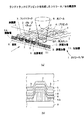
なお、図1(a)は実施形態のDVD−R/Wの断面斜視図であり、図1(b)は当該断面斜視図における矢印方向からグルーブトラックを見た断面図であり、図2はDVD−R/Wに予め記録されているプリ情報及び回転制御情報の記録フォーマットを示す模式図である。
【0026】
先ず、図1を用いて本実施形態のDVD−R/Wの物理的構造について説明する。
【0027】
図1(a)及び(b)において、DVD−R/W1は相変化薄膜からなる記録層11を備えた複数回の情報の書込みが可能な相変化型DVD−R/Wであり、情報が記録されるべきトラックであるグルーブトラック2と当該グルーブトラック2に再生光又は記録光としてのレーザビーム等の光ビームBを誘導するためのランドトラック3とが基板9上に形成されている。
【0028】
また、各グルーブトラック2においては、特に図1(b)に示すように、記録層11を挟むように当該記録層11を保護する機能を有する誘電体層5及び8と、記録された記録情報を再生する際に光ビームBを反射するための金蒸着面6と、記録層11、誘電体層5及び8並びに金蒸着面6を外気から更に保護するための樹脂層9A並びに保護膜7が、夫々基板9上に積層されて形成されている。
【0029】
一方、上記ランドトラック3には上記プリ情報に対応するプリピット4が形成されている。このプリピット4はDVD−R/W1を出荷する前に予め形成されているものである。
【0030】
更に、当該DVD−R/W1においては、グルーブトラック2を当該DVD−R/W1の回転速度に対応する周波数でウォブリングさせている。このグルーブトラック2のウォブリングによる回転制御のための同期信号の記録は、上記プリピット4と同様に、DVD−R/W1を出荷する前に予め実行されるものである。そして、DVD−R/W1に記録情報(プリ情報及び同期信号以外の本来記録すべき画像情報等の情報をいう。以下同じ。)を記録する際には、後述の情報記録装置においてグル−ブトラック2のウォブリングの周波数を検出することにより同期信号を取得してDVD−R/W1を所定の回転速度で回転制御すると共に、プリピット4を検出することにより予めプリ情報を取得し、それに基づいて記録光としての光ビ−ムBの最適出力等が設定されると共に、記録情報を記録すべきDVD−R/W1上の位置であるアドレス情報等が取得され、このアドレス情報に基づいて記録情報が対応する記録位置に記録される。
【0031】
ここで、記録情報の記録時には、光ビームBをその中心がグルーブトラック2の中心と一致するように照射してグルーブトラック2上に記録情報に対応する相変化ピットを形成することにより記録情報を形成する。この時、光スポットSPの大きさは、図1(a)に示すように、その一部がグルーブトラック2だけでなくランドトラック3にも照射されるように設定される。そして、このランドトラック3に照射された光スポットSPの一部の反射光を用いてプッシュプル法(DVD−R/W1の回転方向に平行な分割線により分割された光検出器を用いたラジアルプッシュプル法)によりプリピット4からプリ情報を検出して当該プリ情報が取得されると共に、グルーブトラック2に照射されている光スポットSPの反射光を用いてグルーブトラック2からウォブリング信号が検出されて回転制御用のクロック信号が取得される。
【0032】
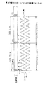
次に、本実施形態のDVD−R/W1に予め記録されているプリ情報及び回転制御情報の記録フォーマットについて、図2を用いて説明する。なお、図2において、上段は記録情報における記録フォーマットを示し、下段の波型波形は当該記録情報を記録するグルーブトラック2のウォブリング状態(すなわち、グルーブトラック2の平面図)を示し、記録情報とグルーブトラック2のウォブリング状態の間の上向き矢印は、プリピット4が形成される位置を模式的に示すものである。ここで、図2においては、グルーブトラック2のウォブリング状態は、理解の容易のため実際の振幅よりも大きい振幅を用いて示してあり、記録情報は当該グルーブトラック2の中心線上に相変化ピットを形成して記録される。
【0033】
図2に示すように、本実施形態においてDVD−R/W1に記録される記録情報は、予めシンクフレーム毎に分割されている。そして、26のシンクフレームにより一のレコーディングセクタが形成され、更に、16のレコ−ディングセクタにより情報ブロックとしての一のECCブロックが形成される。
【0034】
なお、一のシンクフレームは、上記記録情報を記録する際の記録フォーマットにより規定されるビット間隔に対応する単位長さ(以下、Tという。)の1488倍(1488T)の長さを有しており、更に、一のシンクフレームの先頭の14Tの長さの部分にはシンクフレ−ム毎に記録時の同期を取るための同期情報SYが記録される。
【0035】
一方、本実施形態においてDVD−R/W1に記録されているプリ情報は、シンクフレーム毎に記録されている。ここで、プリピット4によるプリ情報の記録においては、記録情報内の夫々のシンクフレームにおける同期情報SYが記録される領域に隣接するランドトラック3上にプリ情報における同期信号を示すものとして必ず一のプリピット4が形成されると共に、当該同期情報SY以外の当該シンクフレーム内の前半部分に隣接するランドトラック3上に記録すべきプリ情報の内容(アドレス情報)を示すものとして二又は一のプリピット4が形成される(なお、同期情報SY以外の当該シンクフレーム内の前半部分については、記録すべきプリ情報の内容によってはプリピット4が形成されない場合もある。また、一のレコーディングセクタの先頭のシンクフレームでは、その前半部分に必ず三つのプリピット4が連続して形成される。)。この際、本実施形態では、一のレコ−ディングセクタにおいては、偶数番目のシンクフレーム(以下、EVENフレームという。)のみ又は奇数番目のシンクフレーム(以下、ODDフレームという。)のみのいずれか一方にプリピット4が形成されてプリ情報が記録される。すなわち、図2において、EVENフレームにプリピット4が形成された場合には(図2において実線上向き矢印で示す。)それに隣接するODDフレームにはプリピット4は形成されない。
【0036】
更に、グルーブトラック2のウォブリングとプリピット4の位置の関係については、当該ウォブリングにおける最大振幅の位置にプリピット4が形成されている。
【0037】
一方、グルーブトラック2は、全てのシンクフレームに渡って140kHz(一のシンクフレームがグルーブトラック2の変動波形の8波分に相当する周波数)の一定ウォブリング周波数でウォブリングされている。そして、後述の情報記録装置において、当該一定のウォブリング周波数を検出することでDVD−R/W1を回転させるためのスピンドルモータの回転制御のための同期信号が検出される。
【0038】
(II)情報記録装置の実施形態
次に、上述した構成を有するDVD−R/W1に対して記録情報を記録するための本発明に係る情報記録装置の実施形態について、図3乃至図17を用いて説明する。
【0039】
なお、以下に説明する情報記録装置は、既に記録情報が記録されているDVD−R/W1上の領域に新たな記録情報を上書き記録する処理(以下、単に上書き記録処理と称する。)と、記録情報が未だ記録されていないDVD−R/W1上の領域に新たに記録情報を記録する処理(以下、追加記録処理と称する。)とが共に可能な情報記録装置である。
【0040】
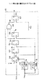
始めに、実施形態に係る情報記録装置の全体構成について、図3を用いて説明する。
【0041】
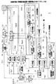
なお、図3は実施形態の情報記録装置の概要構成を示すブロック図である。ここで、当該図3は情報記録装置のうち本発明に係る部分のみを示すブロック図であり、実際の情報記録装置においては、図3に示すブロック図の内容に加えて、トラッキングサーボ制御(実施形態の情報記録装置においては、いわゆる3ビーム法によるトラッキングサーボ制御を用いる。)及びフォーカスサーボ制御(当該情報記録装置においては、いわゆる非点収差法によるフォーカスサーボ制御を用いる。)並びに後述するスピンドルモータの回転制御を行うためのスピンドルサーボ制御夫々のためのサーボ制御系、情報記録装置の動作状態を表示するための表示部及び外部から情報記録装置の動作を指定するための操作部等が含まれている。
【0042】
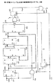
図3に示すように、実施形態の情報記録装置Sは、再生手段としてのピックアップ10と、第2検出手段としてのプリピット検出部11と、タイミングジェネレータ12と、CPU14と、記録手段としてのDVDエンコーダ15と、ストラテジ回路16と、プリピットデコーダ17と、ウォブル検出部18と、スピンドルモータ19と、分周器35と、RF検出部95と、検出手段及び第1検出手段としてのシンク検出部96と、データデコーダ97と、位相変調部EPと、ウォブルPLL(Phase Locked Loop)部WPと、スピンドル制御部SPと、により構成されている。
【0043】
ここで、ピックアップ10は、光ビームBを生成して射出する図示しないレーザダイオード、射出された光ビームBをDVD−R/W1上に集光する図示しない対物レンズ、光ビームBのDVD−R/W1からの反射光に対して上記非点収差法によるフォーカスサーボ制御を行うべく非点収差を与えるための図示しないシリンドリカルレンズ、当該反射光を受光して後述する検出RF信号Spf及び検出信号Spを生成する図示しないディテクタ及び光ビームBの集光位置をDVD−R/W1の半径方向に移動してトラッキングサーボ制御を行うと共にその情報記録面に垂直な方向に移動してフォーカスサーボ制御を行うべく上記対物レンズを当該半径方向又は垂直な方向に移動するための図示しないアクチュエータ等を含んで構成されている。
【0044】
また、本実施形態の情報記録装置Sにおいては、上述したようにフォーカスサーボ制御はいわゆる非点収差法を用いて行われ、更にトラッキングサーボ制御はいわゆる3ビーム法を用いて行われる。そこで、上記ディテクタは、DVD−R/W1の半径方向に平行な分割線を介して互いに隣接すると共にその周方向に平行な分割線を介して互いに隣接する四つの扇形の部分ディテクタからなる主ディテクタ(上記反射光を受光する主ディテクタ)と、上記3ビーム法によるトラッキングサーボ制御用のトラッキングエラー信号を生成するための二つの副ディテクタ(トラッキングサーボ制御のための図示しない二つの副ビーム(すなわち、光ビームBのDVD−R/W1上の集光位置に対してその周方向の前後に一定間隔をおいて夫々照射される二つの副ビーム)を受光するための副ディテクタ)と、により構成されている。そして、当該反射光を受光することで当該主ディテクタから出力される四つの受光信号に基づいて上記検出RF信号Spf及び検出信号Sp並びにフォーカスサーボ制御用のフォーカスエラー信号が生成されると共に、夫々の副ビームの反射光をすることで副ディテクタから夫々出力される二つの受光信号に基づいて上記トラッキングサーボ制御用のトラッキングエラー信号が生成される。
【0045】
一方、位相変調部EPは、分周器20及び24と、位相比較部21及び25と、イコライザ22及び26と、位相シフタ23と、VCO(Voltage Controlled Oscillator)27とにより構成されている。
【0046】
更に、ウォブルPLL部WPは、分周器30及び31と、位相比較部32と、イコライザ33と、VCO34とにより構成されている。
【0047】
更にまた、スピンドル制御部SPは、参照信号発生部40と、分周器41と、位相比較部42と、イコライザ43とにより構成されている。
【0048】
次に、全体動作を説明する。
【0049】
上記上書き記録処理時及び追加記録処理時の双方において、DVD−R/W1に記録すべき記録情報としての記録データSrは、外部から入力され、DVDエンコーダ15において後述するクロック信号Sck及び記録開始信号Ssttに基づき8/16変調され、変調信号Secとしてストラテジ回路16に出力される。この時、当該記録開始信号SsttはDVDエンコーダ15に対して記録データSrの記録の際に一のECCブロック(当該DVDエンコーダ15内で形成されるものである。)の先頭となるべきデータが当該DVDエンコーダ15に入力されるべきタイミングを認識させる機能を有している。
【0050】
そして、ストラテジ回路16において、変調信号Secに対して後述するクロック信号Sckに基づいてDVD−R/W1上に形成される記録ピットの形状を調整するための波形変換が施され、記録信号Srrとしてピックアップ10に出力される。
【0051】
その後、当該ピックアップ10は、記録信号Srrにより強度変調された光ビームBを、記録データSrに対応する相変化ピットを形成すべきグルーブトラック2上に照射し、記録を行う。
【0052】
一方、上書き記録処理時及び追加記録処理時の双方において、当該ピックアップ10は、記録データSrに対応する相変化ピットの形成に先立ち、光ビームBをDVD−R/W1に照射し(図1参照)、上記プリピット4及びグルーブトラック2のウォブリングにより変調された当該光ビームBの反射光を受光して、上記プリピット4及びグルーブトラック2のウォブリングの情報を含む検出信号Spを生成し、プリピット検出部11及びウォブル検出部18へ出力する。
【0053】
次に、プリピット検出部11は、検出信号Spに含まれるプリピット4に対応するプリピット信号Sppを上記ラジアルプッシュプル法により抽出し、当該プリピット信号Sppをタイミングジェネレータ12及びプリピットデコーダ17へ出力する。
【0054】
そして、プリピットデコータ17は、入力されたプリピット信号Sppを後述するクロック信号Sclに基づいてデコードし、一つのECCブロックを記録すべきDVD−R/W1上の領域を示すアドレス信号Satを生成し、上記CPU14に出力する。
【0055】
一方、これらの処理と平行して、上記上書き記録処理時において、RF検出部95は、ピックアップ10から出力される検出RF信号Spfに基づいて、DVD−R/W1上に既に記録されている記録情報に対応する再生RF信号Srfを生成し、タイミングジェネレータ12に出力する。
【0056】
次に、上書き記録処理時において、シンク検出部96は、上記検出RF信号Spfに基づいて、DVD−R/W1上に既に記録されている記録情報における同期情報SY(図2参照)を検出し、各シンクフレームにおける当該同期情報SYの検出が終了したタイミングで「LOW」から「HIGH」に変化するシンク信号Ssyを生成して同じくタイミングジェネレータ12に出力する。
【0057】
更に、上書き記録処理時において、データデコーダ97は、上記検出RF信号Spfに基づいて、当該検出RF信号Spfに含まれている記録情報(既に記録されていた記録情報)が記録されていたDVD−R/W1上の位置を示す再生アドレス情報を含むアドレス信号Saddを生成してCPU14へ出力する。
【0058】
次に、タイミングジェネレータ12は、上記入力された再生RF信号Srf、シンク信号Ssy及びプリピット信号Sppを用いると共に、後述するウォブリング信号Sw及びクロック信号Sck並びにCPU14からの記録データSrの記録を指示する指示信号Srt及び記録位置を検索する等のためにピックアップ10がいわゆるトラックジャンプしたことを示すジャンプ信号Sjpに基づき、これから記録すべき記録情報における一つのECCブロックに対応する上記記録データSrの記録を開始すべきタイミングを示す上記記録開始信号Ssttを生成し、DVDエンコーダ15に出力する。
【0059】
なお、タイミングジェネレータ12は、上記上書き記録処理時においては、再生RF信号Srf、シンク信号Ssy、プリピット信号Spp、ウォブリング信号Sw、クロック信号Sck、指示信号Srt及びジャンプ信号Sjpを用いて記録開始信号Ssttを生成し、一方、上記追加記録処理時においては、再生RF信号Srf及びシンク信号Ssyが検出されないことから、プリピット信号Spp、ウォブリング信号Sw、クロック信号Sck、指示信号Srt及びジャンプ信号Sjpを用いて記録開始信号Ssttを生成する。
【0060】
このとき、上記指示信号Srtは、使用者が上記操作部を操作することにより記録データSrの記録を指示したことをCPU14が検知したときに、上記アドレス信号Satにより取得しているECCブロックを記録すべきDVD−R/W1上の領域を参照して当該CPU14が記録情報の上書き記録処理又は追加記録処理を開始すべきタイミングを指定するために出力する信号である。
【0061】
また、上記ジャンプ信号Sjpは、使用者が上記操作部を操作することにより記録データSrのDVD−R/W1上の記録位置を指示した時等において、これに対応してピックアップ10における光ビームBの照射位置を例えばDVD−R/W1の半径方向に移動させた時に出力されるものであり、このトラックジャンプ時には、上記クロック信号Sckの位相と参照信号発生部40から出力される参照信号(スピンドルモータ19の回転制御のための基準信号ともなるものである。)の位相とがずれる(すなわち、いわゆるロックが外れる)こととなり、これにより正確な記録位置を設定して記録データSrの記録ができなくなるため、当該正確な記録ができない状態になっていることをタイミングジェネレータ12に認識させるべくCPU14が上記ジャンプ信号Sjpを出力するものである。
【0062】
更に、タイミングジェネレータ12は、上書き記録処理時においては、その内部においてプッシュプル信号Spp等に基づいて生成された後述する抽出プッシュプル信号Sgtpをゲートプッシュプル信号Sgppとして位相変調部EP内の位相比較器21の一方の端子に出力すると共に、追加記録処理時においては、上記プッシュプル信号Sppをそのままゲートプッシュプル信号Sgppとして当該位相比較器21の一方の端子に出力する。ここで、当該ゲートプッシュプル信号Sgppは、上書き記録処理時及び追加記録処理時のいずれの場合においてもより正確にプリピット4に対応している信号として位相比較器21へ出力されるものである。
【0063】
次に、検出信号Spが入力されているウォブル検出部18は、当該検出信号Spからグルーブトラック2のウォブリングに対応するウォブル検出信号Swpを生成し、ウォブルPLL部WP内の分周器30並びにスピンドル制御部SP内の位相比較部42へ出力する。
【0064】
そして、ウォブル検出信号Swpが入力されるウォブルPLL部WPは、当該ウォブル検出信号Swpに基づいて、グルーブトラック2のウォブリング周波数に同期した周波数を有するクロック信号Sclを生成し、分周器35及びプリピットデコーダ17に出力すると共に、再度フィードバックのために分周器31に出力する。このため、ウォブルPLL部WPでは、ウォブル検出信号Swpを分周器30により分周した信号とクロック信号Sclを分周器31により分周した信号とを位相比較部32により位相比較し、その比較結果をイコライザ33にて周波数補正した信号を用いてVCO34を駆動し、上記クロック信号Sclを生成している。
【0065】
また、分周器35は、上記クロック信号Sclを再度分周し、上記ウォブリング周波数に対応するウォブリング信号Swを生成して上記タイミングジェネレータ12に出力する。
【0066】
更に、上記ゲートプリピット信号Sgpp及びクロック信号Sclが入力されている位相変調部EPは、それらの信号に基づいて記録データSrの記録時における基準クロックとなる上記クロック信号Sck(その周期は上記T)を生成し、上記DVDエンコーダ15、ストラテジ回路16及びタイミングジェネレータ12に出力すると共に、再度フィードバックのために分周器24に出力する。このため、位相変調部EPでは、始めに、クロック信号Sclを分周器20により分周した信号とゲートプリピット信号Sgppとを位相比較部21により位相比較し、次にその比較結果をイコライザ22にて周波数補正した信号を用いてクロック信号Sclを分周器20により分周した信号の位相を位相シフタ33によりシフトさせ、当該位相シフトした信号とクロック信号Sckを分周器24により分周した信号とを再度位相比較部25により位相比較し、最後にその比較結果をイコライザ26にて周波数補正した信号を用いてVCO27を駆動して上記クロック信号Sckを生成している。
【0067】
一方、上記ウォブル検出信号Swpが入力されるスピンドル制御部SPは、当該ウォブル検出信号Swpに基づいてスピンドルモータ19の回転数を制御して駆動するための駆動信号Sdを生成し、当該スピンドルモータ19に出力する。このため、スピンドル制御部SPでは、参照信号発生部40から出力されるスピンドルモータ19の駆動のための基準信号を分周器41にて分周し、その分周結果と上記ウォブル検出信号Swpとを位相比較部42にて位相比較し、その比較結果の周波数特性をイコライザ43により補正して上記駆動信号Sdを生成している。
【0068】
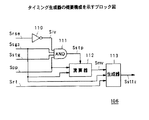
次に、本発明に係るタイミングジェネレータ12の構成及び動作について、図4乃至図17を用いて説明する。
【0069】
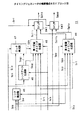
始めに、タイミングジェネレータ12の全体構成について、図4を用いて説明する。なお、図4は当該タイミングジェネレータ12の全体構成を示すブロック図である。
【0070】
図4に示すように、タイミングジェネレータ12は、プリピット信号Spp、ウォブリング信号Sw及びクロック信号Sckを用いて、当該プリピット信号Sppから同期信号に相当するプリピット信号Sppを検出し、検出シンク信号Spsを出力するシンク検出器45と、検出シンク信号Sps及びクロック信号Sckに基づいて、上記クロック信号Sckの位相と参照信号発生部40からの参照信号の位相とがずれることにより正確な記録ができない、いわゆるロックが外れた状態か否かを検出するのに用いられるシンクゲート信号Ssg1及び後述する第1記録タイミング生成器48において記録データSrの記録開始タイミングを予測設定する時に用いられるシンクゲート信号Ssg2とを生成するシンクゲート生成器46と、上記ジャンプ信号Sjp、検出シンク信号Sps及びシンクゲート信号Ssg1を用いて正確な記録が可能なロック状態か否かを示すロック信号Slkを生成するロック検出器47と、上記シンクゲート信号Ssg2、プリピット信号Spp、ロック信号Slk、アドレス信号Sat、クロック信号Sck及び指示信号Srtを用いて、記録データSrの記録開始タイミングを設定するための第1スタート信号Sstt1を生成する第2生成手段及び第2設定手段としての第1記録タイミング生成器48と、上記プリピット信号Spp、ウォブリング信号Sw、ジャンプ信号Sjp、シンク信号Ssy及び指示信号Srtを用いて、記録データSrの記録開始タイミングを設定するための第2スタート信号Sstt2を生成すると共に上記抽出プッシュプル信号Sgtpを生成する生成手段、設定手段、第1生成手段および第2設定手段としての第2記録タイミング生成器49と、再生RF信号Srfに基づいて、DVD−R/W1から当該再生RF信号Srfが検出されるとき、すなわち、上書き記録処理を行うときは上記第2記録スタート信号Sstt2を上記記録開始信号SsttとしてDVDエンコーダ15に出力すると共に、DVD−R/W1から当該再生RF信号Srfが検出されないとき、すなわち、追加記録処理を行うときは上記第1記録スタート信号Sstt1を上記記録開始信号SsttとしてDVDエンコーダ15に出力する選択手段としてのスイッチSW1と、再生RF信号Srfに基づいて、上書き記録処理を行うときは上記抽出プッシュプル信号Sgtpを上記ゲートプッシュプル信号Sgppとして位相比較器21に出力すると共に、追加記録処理を行うときは上記プッシュプル信号Sppをそのままゲートプッシュプル信号Sgppとして位相比較器21に出力するスイッチSW2と、により構成されている。
【0071】
ここで、上記スイッチSW1の動作により、上書き記録処理時においては上記構成のうちのシンク検出器45、シンクゲート生成器46、ロック検出器47及び第1記録タイミング生成器48の動作が有効になると共に、追加記録処理時においては上記構成のうちの第2記録タイミング生成器49の動作が有効になることとなる。
【0072】
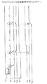
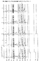
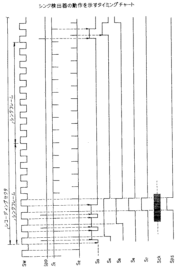
次に、主として追加記録時におけるタイミングジェネレータ12の全体動作(スイッチSW1の動作を除く、追加記録時における上記第1スタート信号Sstt1が生成されるまでの全体動作)について、図5を用いて説明する。なお、図5は追加記録時における当該タイミングジェネレータ12の全体動作を示すタイミングチャートである。
【0073】
先ず、シンク検出器45に対して、図5最上段に示すジャンプ信号Sjp(図5から明らかなように、当該ジャンプ信号Sjpはトラックジャンプ中に「LOW」となり、トラックジャンプしていない時に「HIGH」となる。)が「HIGH」となったタイミングから正規のクロック信号Sckが生成されるまでの予め設定された所定の整定時間だけ経過した後にプリピット4が正規に検出されたことによりプリピット信号Spp(図5上から二段目参照)の入力が開始されると、当該シンク検出器45は、当該プリピット信号Sppにおける一のレコーディングセクタの先頭を示す(すなわち、プリピット4が三つ連続して含まれている)同期信号としてのプリピット信号Sppを検出し、当該プリピット信号Sppが検出されたことを示すパルス信号である検出シンク信号Sps(図5上から三段目参照)を生成する。
【0074】
次に、ロック検出器47は、上記ジャンプ信号Sjpが「HIGH」に変化した後に、上記検出シンク信号Spsと上記シンクゲート信号Ssg1との時間的関係が図5上から三段目及び四段目に示す関係(すなわち、検出シンク信号Spsの立ち上がりタイミングが、シンクゲート信号Ssg1が「HIGH」となっている期間のほぼ中間タイミングとなる関係)となることが予め設定された所定の回数(例えば、最低2回程度)継続すると、正確な記録が可能なロック状態となったとして上記ロック信号Slk(図5上から五段目に示すように、ジャンプ信号Sjpが「LOW」となったときにロック状態が解除されたとして「LOW」に変化し、上記検出シンク信号Spsとシンクゲート信号Ssg1との時間的関係が図5上から三段目及び四段目に示す関係となることが上記所定の回数となったときに再びロック状態に復帰したとして「HIGH」に変化する。)を生成して第1記録タイミング生成器48に出力する。
【0075】
一方、シンクゲート生成器46は、上記検出シンク信号Sps及びクロック信号Sckに基づいて、上記ロック状態か否かを検出するためのシンクゲート信号Ssg1及び記録データSrの記録開始タイミングを予測設定する時に用いられるシンクゲート信号Ssg2とを生成し、夫々ロック検出器47及び第1記録タイミング生成器48に出力する。
【0076】
ここで、当該シンクゲート信号Ssg1は、図5上から四段目に示すように、一の検出シンク信号Spsが正規に生成された場合に、当該検出シンク信号Spsの立ち上がりタイミングがシンクゲート信号Ssg1の「HIGH」となっている期間のほぼ中間タイミングとなるように、過去に検出された検出シンク信号Spsに基づいて生成されるゲート信号である。
【0077】
また、シンクゲート信号Ssg2は、図5下から二段目に示すように、同期信号を示す三つのプリピット4が正規に検出された場合にその先頭のプリピット4が検出されたタイミングがシンクゲート信号Ssg2の「HIGH」となっている期間のほぼ中間タイミングとなるように、同じく過去に検出された検出シンク信号Spsに基づいて生成されるゲート信号である。
【0078】
そして、第1記録タイミング生成器48は、上記シンクゲート信号Ssg2、プリピット信号Spp、ロック信号Slk、クロック信号Sck及び指示信号Srt(図5下から三段目参照。このとき、当該指示信号Srtは、アドレス信号Satに基づきCPU14において判断された追加記録すべき記録データSrの記録が開始されるDVD−R/W1上の記録位置に対応するタイミングよりも当該CPU14において算出された予め設定された時間(具体的には、第1記録タイミング生成器48、スイッチSW1、DVDエンコーダ15及びストラテジ回路16夫々における処理遅延時間並びにピックアップ10内のレーザダイオードの発振遅延時間等を考慮して当該記録位置から正確に記録データSrの記録が開始されるように予め設定された時間)だけ前に「LOW」から「HIGH」に変化する信号である。)を用いて、上記ロック状態にある時に記録データSrの記録開始タイミングを示す上記第1スタート信号Sstt1を生成してスイッチSW1の一方の入力端子に出力する。
【0079】
このとき、当該第1スタート信号Sstt1は、検出シンク信号Spsが正規に生成されている時には当然に出力されるが、たとえプリピット4が検出されずに検出シンク信号Spsが生成されない時でも、後述するシンクゲート信号Ssg2の機能により記録データSrの記録を開始するべきタイミングを予測してそのタイミングを設定可能なように生成されるものである。
【0080】
そして、この後は、上記スイッチSW1により、現在が追加記録処理を行うべきタイミングであれば、生成された第1スタート信号Sstt1が記録開始信号SsttとしてDVDエンコーダ15に出力され、当該DVDエンコーダ15は記録開始信号Ssttにより一のECCブロックの先頭となるべき記録データSrを記録するべきタイミングを認識し、これにより実際の追加記録処理動作が実行される。
【0081】
次に、シンク検出器45の細部構成及び細部動作について、図6及び図7を用いて説明する。なお、図6はシンク検出器45の細部構成を示すブロック図であり、図7はシンク検出器45の細部動作を示すタイミングチャートである。
【0082】
図6に示すように、シンク検出器45は、立上がりエッジ作成回路50と、立下がりエッジ作成回路51と、D型のフリップフロップ回路52、53、54、55及び57と、アンド回路56とにより構成されている。
【0083】
次に、図7を用いてその動作を説明する。なお、シンク検出器45においては、一のレコーディングセクタの先頭のシンクフレームに対応する同期信号としてのプリピット4が、グルーブトラック2のウォブリングにおける最大振幅の位置に連続して三つ形成されていることを利用して当該一のレコーディングセクタの先頭を示すプリピット4を検出し、検出シンク信号Spsを生成している。
【0084】
立上がりエッジ作成回路50に入力されたウォブリング信号Swは、当該立上がりエッジ作成回路50によりその立上がりタイミングが検出され、立上がり信号S1としてフリップフロップ回路52のクリア端子に出力される。また、これと並行して、立下がりエッジ作成回路51に入力されたウォブリング信号Swは、当該立下がりエッジ作成回路51によりその立下がりタイミングが検出され、立下がり信号S2としてフリップフロップ回路53乃至55のクロック端子に出力される。
【0085】
一方、プリピット信号Sppが入力されているフリップフロップ回路52では、当該プリピット信号Sppが入力されたとき「HIGH」」となり、次の立上がり信号S1が入力されるまでの間「HIGH」を維持するので、結局、一のレコーディングセクタの先頭のタイミングでは、図7に示すような連続する三つのパルスを有するタイミング信号S3を生成する。
【0086】
次に、タイミング信号S3が入力されているフリップフロップ回路53では、クロック端子に入力されている立下がり信号S2が「LOW」から「HIGH」となると共にタイミング信号S3が「HIGH」である最初のタイミングから、次に立下がり信号S2のみが「LOW」から「HIGH」となるタイミングまでの間に「HIGH」を維持するタイミング信号S4を生成する。
【0087】
次に、タイミング信号S4が入力されているフリップフロップ回路54では、クロック端子に入力されている立下がり信号S2が「LOW」から「HIGH」となると共にタイミング信号S4が「HIGH」である最初のタイミングから、次に立下がり信号S2のみが「LOW」から「HIGH」となるタイミング(すなわち、タイミング信号S4が「HIGH」から「LOW」に変わるタイミング)までの間に「HIGH」を維持するタイミング信号S5を生成する。このタイミング信号S5は、フリップフロップ回路55に出力されると共にアンド回路56の一方の端子にも出力されている。
【0088】
そして、タイミング信号S5が入力されているフリップフロップ回路55では、クロック端子に入力されている立下がり信号S2が「LOW」から「HIGH」となると共にタイミング信号S5が「HIGH」である最初のタイミングから、次に立下がり信号S2のみが「LOW」から「HIGH」となるタイミング(すなわち、タイミング信号S5及びS4が「HIGH」から「LOW」に変わるタイミング)までの間に「HIGH」を維持するタイミング信号S6を生成する。このタイミング信号S6はアンド回路56の他方の端子に出力されている。
【0089】
そして、アンド回路56において、タイミング信号S5とS6の論理積が算出され、タイミング信号S7が生成される。
【0090】
図6に示す構成を有するシンク検出器45では、三つの連続するプリピット4が検出されなければタイミング信号S7が生成されないこととなるので、結局、当該タイミング信号S7が「HIGH」であるときは、その直前に検出された三つのプリピット4が一のレコーディングセクタの先頭であることを示している。
【0091】
そして、フリップフロップ回路57においてタイミング信号S7とクロック信号Sckとの整合性が取られ、上記検出シンク信号Spsが生成される。
【0092】
次に、シンクゲート生成器46の細部構成及び細部動作について、図8乃至図10を用いて説明する。なお、図8はシンクゲート生成器46の細部構成を示すブロック図であり、図9及び図10はシンクゲート生成器46の細部動作を示すタイミングチャートである。
【0093】
図8に示すように、シンクゲート生成器46は、インバータ60と、D型のフリップフロップ回路61、66及び70と、n進カウンタ62と、コンパレータ63、64、67及び68と、アンド回路65及び69と、により構成されている。ここで、n進カウンタ62は一度計数が開始された後は、計数値が
【数1】
【0094】
上記した構成のうち、インバータ60、フリップフロップ回路61及び66、n進カウンタ62、コンパレータ63及び64並びにアンド回路65が上記シンクゲート信号Ssg1を生成するための回路であり、一方、インバータ60、フリップフロップ回路61及び70、n進カウンタ62、コンパレータ67及び68並びにアンド回路69が上記シンクゲート信号Ssg2を生成するための回路である。
【0095】
次に、図9及び図10を用いてその動作を説明する。なお、図10に示すタイミングチャートは、図9に示すタイミングチャートにおける破線で囲んだタイミングの各信号の波形を拡大表示したものである。
【0096】
始めに、上述したシンクゲート信号Ssg1を生成するための回路の動作について説明する。
【0097】
フリップフロップ回路61のクロック端子には、インバータ60により反転された検出シンク信号Spsが入力されており、一方、クリア端子には各種サーボ制御回路が整定したことを示す信号であって、シンクゲート生成器46によるシンクゲート信号Ssg1及びSsg2の生成を許可する意味を有する上記ジャンプ信号Sjpに基づいて生成されたイネーブル信号Senが入力されている。従って、フリップフロップ回路61の出力であるタイミング信号S10としては、図9上から三段目に示すように、検出シンク信号Spsが「HIGH」から「LOW」に変わるタイミングにおいて「LOW」から「HIGH」に変化する信号が出力される。
【0098】
そして、クロック信号Sckが入力されているn進カウンタ62は、検出シンク信号Spsに基づいて生成されたタイミング信号S10が「HIGH」となることにより一度計数が開始されると、その後にタイミング信号S10が「LOW」となるまで、検出シンクSpsの有無に拘わらず当該クロック信号Sckに含まれるパルスを上記n(=38688T)まで計数した後に「0」に戻ってまたnまで計数する動作を繰り返し、その結果として、検出シンク信号Spsの有無に拘わらず図8に示すような鋸歯状に変化する計数値を含む計数信号Sctを出力する。
【0099】
次に、計数信号Sctが入力されるコンパレータ63では、図10に示すように、当該計数信号Sctの計数値と予め設定された設定値A1に対応する設定値信号Sa1とを常に比較し、当該計数値のほうが設定値A1よりも大きくなったタイミングから次に計数信号Sctの計数値が「0」に戻るまでの間に「HIGH」となる比較信号Sc1を生成し、アンド回路65の一方の入力端子に出力する。
【0100】
ここで、設定値A1は、図10に示すように、同期信号を示すプリピット4が正規に検出された時に上記検出シンクSpsが生成されて「LOW」から「HIGH」に転じるタイミングを含むようにシンクゲート信号Ssg1の立ち上がりタイミングを設定するものであり、より具体的には、計数信号Sctが初期化されてから(すなわち、計数値が「0」となってから)38409T(一のレコーディングセクタ周期に対応する期間からウォブリング周期の1.5倍を引いた値。すなわち、
【数2】
1488T(1シンクフレーム)×26−186T×1.5
=38409T
であり、これは、検出シンク信号Spsとレコーディングセクタの先頭のプリピット4の関係が図7に示す関係にあることによる。)だけ計数されたタイミングを示すものである。
【0101】
一方、計数信号Sctが同様に入力されるコンパレータ64では、当該計数信号Sctの計数値と予め設定された設定値B1に対応する設定値信号Sb1とを常に比較し、当該計数値のほうが設定値B1よりも大きくなったタイミングから次に計数信号Sctが「0」に戻るまでの間に「LOW」となる比較信号Sc2を生成し、アンド回路65の他方の入力端子に出力する。
【0102】
ここで、設定値B1は、図10に示すように、同期信号を示すプリピット4が正規に検出された時に生成された上記検出シンクSpsが「HIGH」から「LOW」に変わるタイミングを含まないようにシンクゲート信号Ssg1の立ち下がりタイミングを設定するものであり、より具体的には、計数信号Sctが「0」に戻ってから38595T(一のレコーディングセクタに対応する期間からウォブリング周期の0.5倍を引いた値。すなわち、
【数3】
1488T(1シンクフレーム)×26−186T×0.5
=38595T
であり、これは、設定値A1と同様に検出シンク信号Spsとレコーディングセクタの先頭のプリピット4の関係が図7に示す関係にあることによる。)だけ計数されたタイミングを示すものである。
【0103】
そして、上記比較信号Sc1及びSc2が入力されているアンド回路65では、これらの論理積を演算し、積信号Sm1を生成してフリップフロップ回路66に出力する。
【0104】
次に、フリップフロップ回路66において積信号Sm1とクロック信号Sckとの整合性が取られ、ロック状態か非ロック状態かを示す信号を生成するための上記シンクゲート信号Ssg1が生成される。
【0105】
なお、当該シンクゲート信号Ssg1については、一度生成された後は、いわゆるフリーランカウンタ等を用いれば当該シンクゲート信号Ssg1を出力し続けるように構成することができる。
【0106】
次に、上述したシンクゲート信号Ssg2を生成するための回路の動作について説明する。
【0107】
当該シンクゲート信号Ssg2を生成するための回路のうち、フリップフロップ回路61、インバータ60及びn進カウンタ62は、上述したシンクゲート信号Ssg1を生成するための回路における場合と同時並行的に同じ動作を行い、計数信号Sctを出力する。
【0108】
次に、計数信号Sctが入力されるコンパレータ67では、当該計数信号Sctの計数値と予め設定された設定値A2に対応する設定値信号Sa2とを常に比較し、当該計数値のほうが設定値A2よりも大きくなったタイミングから次に計数信号Sctが初期化されるまでの間に「HIGH」となる比較信号Sc3を生成し、アンド回路69の一方の入力端子に出力する。
【0109】
ここで、設定値A2は、図10に示すように、三つ連続するプリピット信号Sppのうちの先頭のパルスのタイミングに対応するウォブリング信号Swのパルスが「HIGH」に変わるタイミングを示すものであり、より具体的には、計数信号Sctが初期化されてから(すなわち、計数値が「0」となってから)38037T(一のレコーディングセクタ周期に対応する期間からウォブリング周期の3.5倍を引いた値。すなわち、
【数4】
1488T(1シンクフレーム)×26−186T×3−93T
=38037T
であり、これは、検出シンク信号Spsとレコーディングセクタの先頭のプリピット4の関係が図7に示す関係にあることによる。)だけ計数されたタイミングを示すものである。
【0110】
一方、計数信号Sctが同様に入力されるコンパレータ68では、当該計数信号Sctの計数値と予め設定された設定値B2に対応する設定値信号Sb2とを常に比較し、当該計数値のほうが設定値B2よりも大きくなったタイミングから次に計数信号Sctが「0」に戻るまでの間に「LOW」となる比較信号Sc4を生成し、アンド回路69の他方の入力端子に出力する。
【0111】
ここで、設定値B2は、図10に示すように、三つ連続するプリピット信号Sppのうちの先頭のパルスのタイミングに対応するウォブリング信号Swのパルスが「LOW」に変わるタイミングを示すものであり、より具体的には、計数信号Sctが初期化されてから38130T(一のレコーディングセクタに対応する期間からウォブリング周期の3倍を引いた値。すなわち、
【数5】
1488T(1シンクフレーム)×26−186T×3
=38130T
であり、これは、設定値B1と同様に検出シンク信号Spsとレコーディングセクタの先頭のプリピット4の関係が図7に示す関係にあることによる。)だけ計数されたタイミングを示すものである。
【0112】
そして、上記比較信号Sc3及びSc4が入力されているアンド回路69では、これらの論理積を演算し、積信号Sm2を生成してフリップフロップ回路70に出力する。
【0113】
次に、フリップフロップ回路70において積信号Sm2とクロック信号Sckとの整合性が取られ、一のレコーディングセクタの先頭のタイミングを示す上記シンクゲート信号Ssg2が生成される。
【0114】
なお、当該シンクゲート信号Ssg2については、上記シンクゲート信号Ssg1と同様に、一度生成された後は、いわゆるフリーランカウンタ等を用いれば当該シンクゲート信号Ssg2を出力しつづけるように構成することができる。
【0115】
次に、ロック検出器47の細部構成及び細部動作について、図11及び図12を用いて説明する。なお、図11はロック検出器47の細部構成を示すブロック図であり、図12はロック検出器47の細部動作を示すタイミングチャートである。
【0116】
図11に示すように、ロック検出器47は、インバータ71、73、76、77及び80と、D型のフリップフロップ回路72及び81と、n進カウンタ74及び78と、コンパレータ75及び79と、により構成されている。
【0117】
このうち、インバータ71及び73、フリップフロップ回路72、n進カウンタ74及びコンパレータ75が、それまでクロック信号Sckの位相と参照信号発生部40からの参照信号の位相とがずれてロックが外れた状態だったものが再びロック状態となって記録データSrの記録が可能となったことを検出する回路(すなわち、上記ロック信号Slkの立ち上がりタイミングを設定する回路)であり、インバータ71、76、77及び80、フリップフロップ回路72、n進カウンタ78及びコンパレータ79がそれまでロック状態が保たれていたものが、例えばDVD−R/W1上の傷等により同期信号としてのプリピット4が検出されなかったことに起因して当該ロック状態が外れたことを検出する回路(すなわち、すなわち、上記ロック信号Slkの立ち下がりタイミングを設定する回路)である。
【0118】
次に、ロック検出器47の細部動作について、図12を用いて説明する。
【0119】
始めに、上述したロック状態となったことを検出する回路の動作について、図12(a)を用いて説明する。
【0120】
フリップフロップ回路72の入力端子には上記検出シンク信号Spsがそのまま入力されており、更にクロック端子には上記シンクゲート信号Ssg1をインバータ71により反転した信号が入力されている。
【0121】
ここで、一般に、D型のフリップフロップ回路は、クロック端子に入力されている信号が「HIGH」となったタイミングに入力されている信号の論理(「HIGH」又は「LOW」)となるように当該タイミングで出力される出力信号を更新すると共に、その出力信号の論理をクロック端子に入力されている信号が次に「HIGH」となるまで保持する動作を繰り返す。
【0122】
従って、同期信号としてのプリピット4が正常に検出され、且つ検出シンク信号Spsが正常に生成されているとき(図12最上段中、例えば符号a及びbで示すタイミング)は、フリップフロップ回路72は、図12(a)に示すように、シンクゲート信号Ssg1が「LOW」となったタイミングで、その出力信号S8の論理がそのタイミングに入力されている検出シンク信号Spsの論理となるように当該出力信号S8の論理を更新し、次にシンクゲート信号Ssg1が「HIGH」から「LOW」に切り替るタイミングまでその論理を保持することを繰り返す。よって、検出シンク信号Spsとシンクゲート信号sg1とが正常に生成されているときは、出力信号S8の論理は常に「HIGH」となる。
【0123】
これに対し、例えばDVD−R/W1上の傷等によりプリピット4が正常に検出されず、従って検出シンク信号Spsが正常に生成されなかった場合には(図12最上段中、例えば符号cで示すタイミング)、シンクゲート信号Ssg1が立ち下がったときには検出シンク信号Spsは「LOW」であるので、この立ち下がりタイミングから出力信号S8の論理は「LOW」に転じ、以後、次に検出シンク信号Spsが正常に検出されるまで「LOW」を保持する。
【0124】
そして、次に再び正常に検出シンク信号Spsが検出され始めると(図12最上段中、符号dで示すタイミング)、対応するシンクゲート信号Ssg1が立ち下がるタイミングで出力信号S8の論理は「HIGH」に転じ、以後、これを保持する。
【0125】
次に、当該出力信号S8がイネーブル端子及びクリア端子に入力されているn進カウンタ74では、そのクロック端子に検出シンク信号Spsをインバータ73で反転させた信号が入力されている。
【0126】
ここで、図12に示すn進カウンタ74及び78は、そのイネーブル端子に入力される信号の論理が「LOW」から「HIGH」に転じたときにクロック端子に入力されているパルスの計数を開始して計数信号Snc又はSmcの出力を始め、クリア端子に入力される信号が「HIGH」から「LOW」に転じるタイミングで計数信号Snc又はSmcの計数値を初期化することを繰り返す。
【0127】
従って、図12(a)上から四段目に示すように、検出シンク信号Spsが正常に検出されずフリップフロップ回路72の出力信号S8が「LOW」のときは計数信号Sncの計数値は「0」であり、次に検出シンク信号Spsが生成されて出力信号S8が「HIGH」に転じると(図12(a)中、符号aで示すタイミング)、当該転じたタイミングのときに「HIGH」となっている検出シンク信号Spsが立ち下がるタイミングで計数信号Sncの計数値が「1」だけインクリメントされ、以後計数値が増加していく。
【0128】
そして、次に検出シンク信号Spsが生成されずに出力信号S8が「LOW」に転じると(図12(a)中、符号cで示すタイミング)、その「LOW」に転じたタイミングで計数信号Sncが初期化される。
【0129】
以後は上述の計数動作が繰り返され、次に検出シンク信号Spsが生成されたときから再び計数信号Sncの計数値が増加し始める。
【0130】
次に、計数信号Sncが入力されているコンパレータ75では、当該計数信号Sncの計数値と予め設定された設定値Nに対応する設定値信号Svnとを常に比較し、当該計数値が設定値Nに等しくなっている期間(検出シンク信号Spsにおける一周期)だけ「HIGH」となる比較信号Slc1を生成し、フリップフロップ回路81のクロック端子に出力する。
【0131】
ここで、上記設定値Nは、図12(a)に示すように、検出シンク信号Spsが正常に生成され始めてから確実に上記ロック状態であると判断できるまでに生成されるべき検出シンク信号Spsの数を示すものであり、より具体的な値としては、例えば少なくとも「2」程度であることが必要である。
【0132】
そして、フリップフロップ回路81では、比較信号Slc1が入力されたタイミングでそれまで「LOW」であったロック信号Slkの論理を「HIGH」に転じさせ、以後、当該フリップフロップ回路81のクリア端子に後述する反転比較信号Svlc2が入力されるまでロック信号Slkの「HIGH」の論理を保持する。
【0133】
なお、図12(a)に示すように、ロック信号Slkが「HIGH」となったときにはジャンプ信号Sjpは「HIGH」となっていることはいうまでもない。
【0134】
次に、上述したロック状態が外れたことを検出する回路の動作について、図12(b)を用いて説明する。
【0135】
まず、インバータ71及びフリップフロップ回路72の動作は、上述したロック状態となったことを検出する回路と同様であるので、細部の説明は省略する。
【0136】
次に、当該出力信号S8の論理をインバータ76及び77により反転させた信号がイネーブル端子及びクリア端子に夫々入力されているn進カウンタ78では、そのクロック端子にシンクゲート信号Ssg1をインバータ71で反転させた信号が入力されている。
【0137】
従って、図12(b)上から四段目に示すように、検出シンク信号Spsが正常に検出されて出力信号S8が「HIGH」のときはn進カウンタ78における計数動作は開始されず、計数信号Smcの計数値は「0」である。
【0138】
次に検出シンク信号Spsが生成されなくなり出力信号S8が「HIGH」から「LOW」に転じると(図12(b)上から三段目中、符号eで示すタイミング)、そのタイミングからn進カウンタ78におけるシンクゲート信号Ssg1を反転させた信号のパルスの計数動作が開始され、以後、シンクゲート信号Ssg1が「HIGH」から「LOW」に転じるタイミング毎に計数信号Smcの計数値が「1」だけインクリメントされる動作が繰り返される(図12(b)上から三段目及び四段目中、符号fで示すタイミング以降)。
【0139】
そして、次に検出シンク信号Spsが生成されて出力信号S8が「HIGH」に転じる(図12(a)上から三段目参照)と、その「HIGH」に転じたタイミングで計数信号Smcが初期化される。
【0140】
以後は上述の計数動作が繰り返され、次に検出シンク信号Spsが生成されなくなったときから再び計数信号Smcの計数値が増加し始める。
【0141】
次に、計数信号Smcが入力されているコンパレータ79では、当該計数信号Smcの計数値と予め設定された設定値Mに対応する設定値信号Svmとを常に比較し、当該計数値が設定値Mに等しくなっている期間(検出シンク信号Spsにおける一周期)だけ「HIGH」となる比較信号Slc2を生成し、これをインバータ80によりその論理を反転させて反転比較信号Svlc2とした後にフリップフロップ回路81のクリア端子に出力する。
【0142】
ここで、上記設定値Mは、図12(b)上から四段目に示すように、検出シンク信号Spsが生成されなくなってから確実に上記ロック状態が外れたと判断できるまでに生成されなかった検出シンク信号Spsの数を示すものであり、より具体的な値としては、例えば「5」又は「6」程度が適当である。
【0143】
そして、フリップフロップ回路81では、比較信号Slc1により「HIGH」に転じているロック信号Slkの論理を、比較信号Slc2が「LOW」から「HIGH」に転じたタイミングで再び「LOW」に転じさせ(図12(b)最下段参照。)、以後、次に上記比較信号Slc1が「LOW」から「HIGH」に転じるまで「LOW」の論理を保持する。
【0144】
以上のロック検出器47の動作により、ロック状態が確立された時に「HIGH」に転じると共に当該ロック状態が外れたことが確立された時に「LOW」に転じる上記ロック信号Slkが生成されて記録タイミング生成器48へ出力される。
【0145】
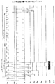
次に、第1記録タイミング生成器48の細部構成及び細部動作について、図13及び図14を用いて説明する。なお、図13は第1記録タイミング生成器48の細部構成を示すブロック図であり、図14は第1記録タイミング生成器48の細部動作を示すタイミングチャートである。
【0146】
図13に示すように、記録タイミング生成器48は、n進カウンタ85と、二入力のアンド回路86及び94と、D型のフリップフロップ回路87、89、91及び93と、加算器88と、コンパレータ90と、三入力のアンド回路92と、により構成されている。
【0147】
次に、第1記録タイミング生成器48の細部動作について、図14を用いて説明する。なお、図14最上段は、一のレコーディングセクタ夫々の先頭のプリピット4における同期信号に関る部分のみを示すものであり、また、破線で示すパルスは、本来そのタイミングで検出されるべきプリピット4がDVD−R/W1の傷等により検出されなかった場合を示している。
【0148】
アンド回路86には、プリピット信号Spp(図14最上段参照)及び上記シンクゲート信号Ssg2(図14上から二段目参照)が入力されており、その両者が「HIGH」のときのみ積信号Saを生成してフリップフロップ回路87及び89のクロック端子に出力する。従って、プリピット4が正常に検出されないときは当該積信号Saは「LOW」のままであり、フリップフロップ87及び89の後述する出力信号Sc及びSadがそのタイミングで更新されることはない。
【0149】
一方、シンクゲート信号Ssg2がイネーブル端子及びクリア端子に、クロック信号Sck(図14上から四段目参照)がクロック端子に夫々入力されているn進カウンタ85は、シンクゲート信号Ssg2が「LOW」から「HIGH」に転じるタイミングからクロック信号Sckにおけるパルスの計数を開始しその計数値に対応する計数信号Sctt(図14上から五段目参照。)を出力し、シンクゲート信号Ssg2が次に「HIGH」から「LOW」に転じるタイミングで当該計数を停止して計数信号Scttの計数値を「0」に初期化することを、シンクゲート信号Ssgのパルスが入力される度に繰り返す。
【0150】
次に、フリップフロップ回路87は、その入力端子に入力されている計数信号Scttの計数値のうち、クロック端子に入力されている積信号Saが「HIGH」になったときの当該計数値を保持し出力信号Scとしてその後出力し続けると共に、次に積信号Saが「HIGH」になったときにそれまでの出力信号Scに含まれる計数値を当該次に積信号Saが「HIGH」になったタイミングに入力端子に入力されている計数信号Scttの計数値に更新して保持しその後出力し続けることを、積信号Saのパルスが入力される度に繰り返す。
【0151】
従って、上述のように、プリピット4が検出されずに積信号Saが「LOW」のままの時は、出力信号Scに含まれている計数値が計数信号Scttの値に更新されることはなく、それまでの値が保持され続ける(図14最上段中符号「a」乃至「c」で示される期間参照)。
【0152】
一方、上記出力信号Scとフリップフロップ回路89の出力信号Sadとが入力されている加算器88は、同じビット数(例えば、nビットとする。)を有する出力信号Scと出力信号Sadとを加算してnビットの加算信号Sddとして出力するので、結果として、加算信号Sddは、出力信号Scに含まれている計数値と出力信号Sadに含まれている計数値との平均値に相当する値を有することとなる(図14上から七段目参照)。
【0153】
次に、フリップフロップ回路89は、その入力端子に入力されている加算信号Sddの値のうち、クロック端子に入力されている積信号Saが「HIGH」になったときの当該値を保持し出力信号Sad(図14下から六段目参照)としてその後加算器88及びコンパレータ90に出力し続けると共に、次に積信号Saが「HIGH」になったときにそれまでの出力信号Sadに含まれる計数値を当該次に積信号Saが「HIGH」になったタイミングに入力端子に入力されている加算信号Sddの値に更新して保持しその後出力し続けることを、積信号Saのパルスが入力される度に繰り返す。
【0154】
従って、上述のように、プリピット4が検出されずに積信号Saが「LOW」のままの時は、出力信号Sadに含まれている計数値が加算信号Sadの値に更新されることはなく、それまでの値が保持されつ続ける(図14最上段中符号「a」乃至「c」示される期間参照)
次に、出力信号Sadと上記計数信号Scttとが夫々別個に入力されているコンパレータ90では、当該出力信号Sadに含まれる計数値と計数信号Scttに含まれる計数値とを常に比較し、双方の計数値が等しくなったタイミング(具体的には、例えば、図14中符号「a」で示されるシンクゲート信号Ssg2における場合では、n進カウンタ85の計数動作が開始されたタイミングにおける出力信号Sadに含まれる計数値(図14下から六段目においてMn-1で示される値)と計数信号Scttに含まれる計数値とが一致したタイミング)で「HIGH」となる比較信号Sf(図14下五段目参照)を生成し、アンド回路92の一の入力端子に出力する。
【0155】
ここで、当該比較信号Sfは、これまで説明したフリップフロップ回路87及び89並びに加算器88の動作により、プリピット4が正常に検出されない場合でも、フリップフロップ回路89に保持されている計数値に対応するタイミングで「HIGH」となる。
【0156】
次に、記録データSrを記録すべきDVD−R/W1上の記録位置に対して一レコーディングセクタ分だけ前の記録位置を示す指示信号Srtが図14下から三段目に示すタイミングで入力されたとすると、フリップフロップ回路91は、指示信号Srtが「HIGH」となったタイミング以降に「HIGH」となり続ける出力信号Sg(図14下から二段目参照)を生成してアンド回路92の第二の入力端子に出力する。このとき、当該出力信号Sgは、ピックアップ10が光ビームBを照射している位置が、記録データSrを記録すべき位置が含まれるレコーディングセクタの一つ前のレコーディングセクタの位置であることを示していることとなる。
【0157】
一方、アンド回路92は、夫々入力されている出力信号Sad及びSg、並びにロック信号Slkが全て「HIGH」の時に、タイミング信号Sffを出力する。従って、当該タイミング信号Sffは、検出シンク信号Spsが安定に生成されて(すなわち、プリピット4が正常に検出されて)ロック状態となっていると共に、記録データSrを記録すべき位置が含まれるレコーディングセクタの一つ前のレコーディングセクタを光スポットSPが照射中であり、且つ、現在記録データSrを記録すべき位置を設定するための基準となるタイミングであるときに「HIGH」となる。
【0158】
次に、フリップフロップ回路93は、指示信号Srtが「HIGH」であるときは、入力されるタイミング信号Sffをタイミング信号Svgとしてそのままアンド回路94に出力する。
【0159】
そして、アンド回路94は、タイミング信号Svgと指示信号Srtとが共に「HIGH」である時に「HIGH」となる上記第1スタート信号Sstt1(図14最下段参照)を生成して、上記スイッチSW1に出力する。
【0160】
次に、主として上書き記録処理時においてその動作が有効となる第2記録タイミング生成器49の細部構成及び細部動作について、図15乃至図17を用いて説明する。なお、図15は第2記録タイミング生成器49の細部構成を示すブロック図であり、図16はタイミング生成器106の細部構成を示すブロック図であり、図17は上書き記録処理時における当該第2記録タイミング生成器49を含めた情報記録装置S全体の動作を示すタイミングチャートである。また、図17に示されているプッシュプル信号Sppにおいて、無印の破線で示されているパルスは、本来検出されるべきタイミングであるにも拘らず隣接して形成されている同期情報SYを示す相変化ピットの影響により検出されない状況を示しており、一方、丸印付きの破線で示されているパルスは、本来検出されないタイミングで当該相変化ピットの影響により恰もプリピット信号Sppのようなパルス信号が検出されている状況を示している。
【0161】
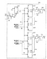
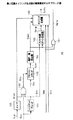
図15に示すように、第2記録タイミング生成器49は、タイマ100と、シンクナンバデコーダ101と、ナンド回路102と、計数手段としてのフリーランカウンタ103と、ゲート信号生成手段としての位置・幅設定器104と、セクタ先頭ゲート生成器105と、タイミング信号生成手段としてのタイミング生成器106と、アンド回路107と、により構成されている。
【0162】
また、図16に示すように、タイミング生成器106は、インバータ110と、アンド回路111と、演算器112と、生成器113と、により構成されている。
【0163】
次に、第2記録タイミング生成器49の動作を中心とした上書き記録処理時における情報記録装置Sの動作について、図15乃至図17を用いて説明する。なお、図17上から三段目に示されている再生RF信号Srfのうち、斜線部分は既にDVD−R/W1に記録されていた記録情報の部分を示し、白抜き部分は同期情報SY(図2参照)の部分を示している。
【0164】
先ず、上記ジャンプ信号Sjpが入力されているタイマ100は、当該ジャンプ信号Sjpが「HIGH」から「LOW」に変化したタイミング(すなわち、上記ロック状態が外れたタイミング)から計時を開始し予め設定された同期情報検出期間だけ経過したときに当該計時を終了することを、ジャンプ信号Sjpが「HIGH」から「LOW」に変化する度に繰り返す。そして、この計時処理により、ジャンプ信号Sjpが「HIGH」から「LOW」に変わったタイミングで「LOW」から「HIGH」に変化し、且つタイマ100における計時が終了したときに「HIGH」から「LOW」に変化するリシンクイネーブル信号Srseが生成されナンド回路102及びタイミング生成器106へ出力される。
【0165】
ここで、当該同期情報検出期間とは、ジャンプ信号Sjpが「HIGH」から「LOW」に変化したタイミングから各種サーボ制御が再開されるまでの予め設定された上記整定時間(図5参照)経過後に少なくとも一パルス上記シンク信号Ssyが検出される時間として予め設定されている時間であり、より具体的には、当該整定時間経過後少なくとも一レコーディングセクタ分の検出RF信号Srfが検出される期間内にDVD−R/W1上の傷等により同期情報SYが検出できない場合を考慮したマージン時間を加えた期間とされる。
【0166】
一方、これと並行して、シンクナンバデコーダ101は、入力されるシンク信号Ssyにおける各同期情報SYの内容を解読し、一のレコーディングセクタにおける最後のシンクフレームにおける同期情報SYが検出された直後に「HIGH」に変化し、一シンクフレームに対応する長さだけ経過した後に「LOW」に変化する最終シンクナンバ信号Slnを生成してナンド回路102の一の入力端子及びセクタ先頭ゲート生成器105へ出力する。
【0167】
ここで、当該同期情報SYは、一のシンクフレームの先頭を示すタイミング情報としての意味を持つと共に、その内容としては、それが含まれているシンクフレームが一のレコーディングセクタにおける何番目のシンクフレームであるかを示すナンバ情報(その値は、「0」から「25」の範囲を取る。)が含まれている。従って、上記最終シンクナンバ信号Slnは、その中のナンバ情報の値が「25」である同期情報SYに対応するシンク信号Ssyが入力されたタイミングから一シンクフレーム分だけ「HIGH」となって出力されることとなる。換言すれば、最終シンクナンバ信号Slnが「HIGH」から「LOW」に変化したタイミングは、一のレコーディングセクタにおける先頭のシンクフレーム内の同期情報SYが検出し終わった直後のタイミングと同一であるということになる(図17上から三段目及び同五段目参照)。
【0168】
次に、ナンド回路102は、シンク信号Ssy(図17上から三段目及び同四段目に示すように、検出される再生RF信号Srfの同期情報SYが終了したタイミングで「LOW」から「HIGH」に変化するパルス信号とされている。)、リシンクイネーブル信号Srse及び最終シンクナンバ信号Slnが共に「HIGH」となったときに「HIGH」から「LOW」に変化し、シンク信号Ssyが「HIGH」から「LOW」に変化したタイミングで「LOW」から「HIGH」に変化するリシンク信号Srsを生成し、フリーランカウンタ103に出力する。
【0169】
この処理により、当該リシンク信号Srsは、一のレコーディングセクタにおける最終シンクフレーム内の同期情報SYが検出され終わったタイミングを示す信号となる。
【0170】
次に、フリーランカウンタ103は、リシンク信号Srsが「HIGH」から「LOW」に変化したタイミングでリセットされると共に、一のシンクフレームに対応する数(具体的には、図2により「8」となる。)だけ上記ウォブリング信号Swにおけるパルスを計数したときにリセットされることを繰り返しつつ当該ウォブリング信号Swにおけるパルスの計数を行い、その計数結果が予め設定されている閾値THとなったタイミングを示すカウント信号Scntを生成して位置・幅設定器104へ出力する。このとき、当該閾値THは、図17上から八段目に示すように、一のシンクフレームに相当する期間から同期情報SYが検出される期間だけ減じた期間(すなわち、一のシンクフレームにおける記録情報のみに対応する時間)Tに計数されるべきウォブリング信号Swのパルスの数と等しい値とされる。この処理により、リシンク信号Srsが上述したように一のレコーディングセクタの最後のシンクフレームにおける同期情報SYが検出され終わったタイミングを示していることから、ジャンプ信号Sjpが「LOW」から「HIGH」に変化した以降に始めてカウント信号Scntが「HIGH」となるタイミング(図17中符号*で示す。)は、一のレコーディングセクタにおける先頭のシンクフレームが開始されるタイミングを示すこととなる。そして、それ以降に生成されるカウント信号Scntは、当該一のレコーディングセクタ内の後続する各シンクフレームの先頭のタイミングを示していることとなる。
【0171】
次に、位置・幅設定器104は、カウント信号Scntが「HIGH」となったタイミング(すなわち、一のシンクフレームが開始されるタイミング)から同期情報SYに対応する期間に検出されるべきプリピット4に対応するプリピット信号Sppのパルスのみが含まれるべき期間(通常は、当該同期情報SYが検出される期間)だけ「HIGH」となるシンクゲート信号Ssg3を生成してセクタ先頭ゲート生成器105、タイミング生成器106及びアンド回路107へ出力する。このシンクゲート信号Ssg3は上述の通りプリピット信号Sppには依存せずに生成されるので、同期情報SYの位置に対応するプリピット4がDVD−R/W1上の傷等の理由により検出されなくとも、当該プリピット4が検出されるであろう期間を正確に示す信号として生成される。
【0172】
次に、セクタ先頭ゲート生成器105は、最終シンクナンバ信号Sln及びシンクゲート信号Ssg3に基づいて、当該最終シンクナンバ信号Slnをシンクゲート信号Ssg3によりラッチし、これにより、最終シンクナンバ信号Slnが「HIGH」となっている期間中であってシンクゲート信号Ssg3が「HIGH」となったタイミングで「LOW」から「HIGH」に変化し、且つ一のシンクフレームに相当する期間だけ「HIGH」状態を継続するセクタ先頭ゲート信号Sstg(図17上から六段目参照)を生成してタイミング生成器106へ出力する。この処理により、セクタ先頭ゲート信号Sstgが「HIGH」の期間に生成されるシンクゲート信号Ssg3が一のレコーディングセクタの先頭を示すシンクゲート信号Ssg3であることが認識できることとなる。
【0173】
次に、タイミング生成器106内のインバータ110は、上記リシンクイネーブル信号Srseを反転し、反転信号Sivを生成してアンド回路111の一の入力端子に出力する。
【0174】
これによりアンド回路111は、上記反転信号Siv、シンクゲート信号Ssg3、セクタ先頭ゲート信号Sstg及びプッシュプル信号Sppが全て「HIGH」であるときのみ「HIGH」となるセクタ先頭タイミング信号Sstpを生成して演算器112へ出力する。この処理により、セクタ先頭タイミング信号Sstpは、一のレコーディングセクタの先頭のシンクフレームにおける同期情報SYに対応するプリピット信号Sppが入力されたタイミングを示すこととなる。
【0175】
次に、演算器112は、セクタ先頭タイミング信号Sstpが入力されるタイミング毎(すなわち、各レコーディングセクタの先頭が検出される毎)に、入力されているシンクゲート信号Ssg3が「HIGH」となるタイミングから図示しない基準クロックの計数を開始し、当該シンクゲート信号Ssg3内にプリピット信号Sppが検出されたときにその計数を終了し、その計数結果(図17下から三段目において符号n1及びn2で示す。)を蓄積する動作を繰り返す。このとき、当該計数処理は、シンクゲート信号Ssg3内に含まれるプリピット信号Sppがその近傍に形成されている同期情報SYを示すピットの影響により検出されないときには実行されない。そして、演算器112は、当該計数処理が終了する度に算出された新たな計数値をそれまでの計数値の平均値に加算した後に更に平均する動作を繰り返し、新たに算出された平均値を示す演算値信号Smvを生成して生成器113へ出力する。
【0176】
この処理により、演算値信号Smvにより示される平均値mは、各レコーディングセクタの先頭に相当するシンクゲート信号Ssg3と当該シンクゲート信号Ssg3に対応するプリピット信号Sppとの位置関係を示す計数値(図17の場合は計数値n1及びn2)の平均値を常に更新しつつ算出された最新の(換言すれば、各レコーディングセクタの先頭におけるシンクゲート信号Ssg3とプリピット信号Sppと時間的関係として最も確からしい)当該位置関係を、双方の信号の時間的ずれの量として示すこととなる。
【0177】
次に、生成器113は、上記指示信号Srtにより記録データSrを開始すべきECCブロックの先頭のタイミングが到来することが示されると、当該指示信号Srtが「HIGH」に変化した直後に入力されるシンクゲート信号Ssg3が「HIGH」に変化したタイミングから演算値信号Smvにより示される平均値mに対応する時間だけ経過したタイミング以降に「HIGH」となる第2スタート信号Sstt2(図17最下段参照)を生成してスイッチSW2の一方の入力端子に出力する。
【0178】
ここで、当該指示信号Srtの生成については、記録を開始すべき記録データSrの最初のECCブロックを記録すべきDVD−R/W1上の記録位置を当該CPU14が図示しない操作部における記録開始操作に基づいて認識すると、次に,CPU14が当該記録位置に相当するDVD−R/W1上のアドレス(以下、このアドレスを所望アドレスと称する。)から二つ前のレコーディングセクタを示すアドレスが検出されたことを当該CPU14に入力されているアドレス信号Saddを参照して確認し、次に所望アドレスから一つ前のレコーディングセクタに相当する期間に「LOW」から「HIGH」に変化する上記指示信号Srtを生成して当該生成器113へ出力するものである。なお、この指示信号Srtが「HIGH」に変化するタイミングとしては、当該所望アドレスから一つ前のレコーディングセクタに相当する期間のうちなるべく早期のタイミングであることが望ましい。
【0179】
一方、これらの処理と平行して、アンド回路107は、シンクゲート信号Ssg3とプリピット信号Sppとが共に「HIGH」となるタイミングで「HIGH」となる上記抽出プッシュプル信号Sgtpを生成してスイッチSW2の一方の入力端子に出力する。これにより、再生RF信号Srfを基準として各シンクフレームの先頭のプリピット4により確からしく対応するプリピット信号Sppである抽出プリピット信号Sgtpを生成できることとなる。
【0180】
以上説明したように、実施形態の情報記録装置Sの動作によれば、既に記録されている記録情報中の同期情報SYに基づいて上書き記録処理する記録データSrの記録開始タイミングを設定するので、記録情報が既に記録されているDVD−R/W1からプリピット信号Sppが検出されない場合でも、正確に記録開始タイミングを設定して記録データSrの記録を開始することができる。
【0181】
また、上書き記録処理する記録データSrを記録する際にプリピット信号Sppが検出されるべきタイミングを含むシンクゲート信号Ssg3と既に検出されたプリピット信号Sppとに基づいて記録開始タイミングを予測し設定するので、より正確に記録開始タイミングを設定することができる。
【0182】
更に、フリーランカウンタ103の計数結果と予め設定されている閾値THとを比較することによりシンクゲート信号Ssg3を生成するので、簡易な構成でシンクゲート信号Ssg3を生成して記録開始タイミングを設定することができる。
【0183】
更にまた、タイミング生成器106が記録データSrにおけるECCブロックの記録を開始するタイミング設定するので、ECCブロック毎の記録開始タイミングを正確に設定することができる。
【0184】
また、記録情報が既に記録されているDVD−R/W1に対して記録データSrを上書き記録する場合及び記録情報が未だ記録されていないDVD−R/W1に対して記録データSrを追加記録する場合の双方において、シンクフレームの先頭を示すプリピット信号Sppが検出されない場合でも、上書き記録処理又は新たに追加記録処理すべき記録データSrに対応する記録開始位置を正確に設定して記録を開始することが可能となる。
【図面の簡単な説明】
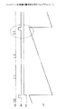
【図1】ランドトラックにプリピットを形成したDVD−R/Wの構造例を示す図であり、(a)はその斜視図であり、(b)はその断面図である。
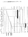
【図2】実施形態のDVD−R/Wにおける記録フォーマットを示す図である。
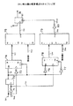
【図3】実施形態の情報記録装置の概要構成を示すブロック図である。
【図4】タイミングジェネレータの概要構成を示すブロック図である。
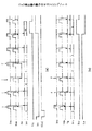
【図5】タイミングジェネレータの全体動作を示すタイミングチャートである。
【図6】シンク検出器の構成を示すブロック図である。
【図7】シンク検出器の動作を示すタイミングチャートである。
【図8】シンクゲート生成器の構成を示すブロック図である。
【図9】シンクゲート生成器の動作を示すタイミングチャート(I)である。
【図10】シンクゲート生成器の動作を示すタイミングチャート(II)である。
【図11】ロック検出器の概要構成を示すブロック図である。
【図12】ロック検出器の動作を示すタイミングチャートである。
【図13】第1記録タイミング生成器の概要構成を示すブロック図である。
【図14】第1記録タイミング生成器の動作を示すタイミングチャートである。
【図15】第2記録タイミング生成器の概要構成を示すブロック図である。
【図16】タイミング生成器の概要構成を示すブロック図である。
【図17】第2記録タイミング生成器の動作を示すタイミングチャートである。
【符号の説明】
1…DVD−R/W
2…グルーブトラック
3…ランドトラック
4…プリピット
5…誘電体層
6…金蒸着膜
7…保護膜
8…誘電体層
9…基板
9A…樹脂層
10…ピックアップ
11…プリピット検出部
12…タイミングジェネレータ
14…CPU
15…DVDエンコーダ
16…ストラテジ回路
17…プリピットデコーダ
18…ウォブル検出部
19…スピンドルモータ
20、24、30、31、35、41…分周器
21、25、32、42…位相比較部
22、26、33、43…イコライザ
23…位相シフタ
27、34…VCO
40…参照信号発生部
45…シンク検出器
46…シンクゲート生成器
47…ロック検出器
48…第1記録タイミング生成器
49…第2記録タイミング生成器
50…立上がりエッジ作成回路
51…立下がりエッジ作成回路
52、53、54、55、57、61、66、70、72、73、81、87、89、91、93…フリップフロップ回路
56、65、69、86、92、94、111…アンド回路
60、71、73、76、77、80…インバータ
62、74、78、85…n進カウンタ
63、64、67、68、75、79、90…コンパレータ
95…RF検出部
96…シンク検出部
97…データデコーダ
100…タイマ
101…シンクナンバデコーダ
102…ナンド回路
103…フリーランカウンタ
104…位置・幅設定器
105…セクタ先頭ゲート生成器
106…タイミング生成器
110…インバータ
112…演算器
113…生成器
EP…位相変調部
WP…ウォブルPLL部
SP…スピンドル制御部
SW1、SW2…スイッチ
S…情報記録装置
B…光ビーム
SY…同期情報
Sp…検出信号
Spp…プリピット信号
Sgpp…ゲートプリピット信号
Sgtp…抽出プリピット信号
Spf…検出RF信号
Srf…再生RF信号
Ssy…シンク信号
Sadd…アドレス信号
Sr…記録データ
Sd…駆動信号
Srr…記録信号
Sec…変調信号
Swp…ウォブル検出信号
Sw…ウォブリング信号
Sck、Scl…クロック信号
Sps…検出シンク信号
S1…立上がり信号
S2…立下がり信号
S3、S4、S5、S6、S7、S10、Sff、Svg…タイミング信号
Sen…イネーブル信号
Sct、Sctt、Snc、Smc…計数信号
Scnt…カウント信号
Sc1、Sc2、Sc3、Sc4、Slc1、Slc2、Sf…比較信号
Svlc2…反転比較信号
Slk…ロック信号
Sm1、Sm2、Sa…積信号
Sa1、Sa2、Sb1、Sb2、Svn、Svm…設定値信号
Ssg1、Ssg2、Ssg3…シンクゲート信号
Sstt…記録開始信号
Sstt1…第1スタート信号
Sstt2…第2スタート信号
Srt…指示信号
S8、Sad、Sg…出力信号
Sdd…加算信号
Sjp…ジャンプ信号
Srse…リシンクイネーブル信号
Srs…リシンク信号
Sln…最終シンクナンバ信号
Sstg…セクタ先頭ゲート信号
Sstp…セクタ先頭タイミング信号
Siv…反転信号
Smv…演算値信号[0001]
BACKGROUND OF THE INVENTION
TECHNICAL FIELD The present invention relates to a recording timing setting device for setting recording timing (recording position) of recording information on a recording medium such as an optical disc and recording the recording information, and an information recording apparatus including the recording timing setting device. Belonging to.
[0002]
[Prior art]
In recent years, DVD-R / W, which is an optical disc capable of improving the recording density several times compared to a CD-R (Compact Disk-Recordable) as a conventional recordable optical disc and capable of recording record information a plurality of times. However, in the information recording apparatus for recording the record information on the DVD-R / W, the DVD-R / W is discrete (in a state where no record information is recorded) in advance. On the DVD-R / W on which recording information is to be recorded, and a recording clock signal serving as a recording reference is generated based on the detected synchronization signal. The address information indicating the position is acquired and recorded.
[0003]
According to this configuration, even if the rotation of the DVD-R / W is deviated from the steady speed due to disturbance, the frequency of the recording clock signal can be shifted in accordance with the deviation. It is possible to generate a recording clock signal having a frequency always synchronized with the rotation and accurately record the recording information.
[0004]
[Problems to be solved by the invention]
However, according to the configuration of the conventional information recording apparatus, when recording information is newly recorded on the DVD-R / W area where no recording information is recorded, the surface of the DVD-R / W is recorded. When the sync signal on the DVD-R / W cannot be detected due to scratches, fingerprints, etc., the recording clock signal cannot be generated in the meantime. There was a problem that it could not be recorded.
[0005]
On the other hand, when new recording information is overwritten on a DVD-R / W area in which recording information has already been recorded, a pit indicating the synchronization signal (in the conventional DVD-R / W, this pit) The pit indicating the synchronization signal is formed as a phase pit at a position on the land track adjacent to the groove track on which the record information is to be recorded. As a result, the detection signal corresponding to the pit indicating the synchronization signal becomes difficult to detect compared to the case where there is no recording information, and as a result, synchronization is accurately performed. There is also a problem that the signal may not be detected.
[0006]
Therefore, the present invention has been made in view of the above-mentioned problems, and the problem is that the recorded information is newly overwritten at least in an area in which recorded information is already recorded on an optical disc such as a DVD-R / W. Provided is a recording timing setting device capable of setting a recording position corresponding to recording information to be overwritten even when the synchronization signal for recording control cannot be detected when recording, and the recording timing device And an information recording apparatus capable of overwriting recording information at an accurate recording position.
[0007]
[Means for Solving the Problems]
In order to solve the above-mentioned problem, the invention according to
[0023]
DETAILED DESCRIPTION OF THE INVENTION
Next, preferred embodiments of the present invention will be described with reference to the drawings. In the embodiment described below, the address information indicating the position on the DVD-R / W where information is to be recorded is recorded as pre-information by forming a pre-pit, and the DVD-R / at the time of recording is recorded. In this embodiment, the present invention is applied to an information recording apparatus for recording information on a DVD-R / W as a recording medium on which the synchronization signal for controlling the rotation speed of W is recorded. .
[0024]
(I)Embodiment of DVD-R / W
First, FIGS. 1 and 2 show an embodiment of a DVD-R / W in which pre-pits corresponding to the pre-information are formed and a groove track described later is wobbled at a predetermined frequency and the sync signal is recorded. Will be described.
[0025]
1A is a cross-sectional perspective view of the DVD-R / W of the embodiment, FIG. 1B is a cross-sectional view of the groove track viewed from the direction of the arrow in the cross-sectional perspective view, and FIG. It is a schematic diagram which shows the recording format of the pre-information and rotation control information previously recorded on DVD-R / W.
[0026]
First, the physical structure of the DVD-R / W of this embodiment will be described with reference to FIG.
[0027]
1 (a) and 1 (b), DVD-R / W1 is a phase change DVD-R / W having a
[0028]
Further, in each
[0029]
On the other hand, a pre-pit 4 corresponding to the pre-information is formed on the
[0030]
Further, in the DVD-R / W1, the
[0031]
Here, at the time of recording the record information, the light beam B is irradiated so that the center thereof coincides with the center of the
[0032]
Next, the recording format of pre-information and rotation control information recorded in advance on the DVD-R /
[0033]
As shown in FIG. 2, the record information recorded on the DVD-R / W1 in this embodiment is divided in advance for each sync frame. Then, one recording sector is formed by 26 sync frames, and one ECC block as an information block is formed by 16 recording sectors.
[0034]
One sync frame has a length of 1488 times (1488T) a unit length (hereinafter referred to as T) corresponding to the bit interval defined by the recording format when recording the recording information. In addition, synchronization information SY for synchronization at the time of recording is recorded for each sync frame in the first 14T length portion of one sync frame.
[0035]
On the other hand, the pre-information recorded on the DVD-R / W1 in this embodiment is recorded for each sync frame. Here, in the recording of the pre-information by the pre-pit 4, it is always necessary to indicate a synchronization signal in the pre-information on the
[0036]
Further, regarding the relationship between the wobbling of the
[0037]
On the other hand, the
[0038]
(II)Embodiment of information recording apparatus
Next, an embodiment of an information recording apparatus according to the present invention for recording record information on a DVD-R /
[0039]
Note that the information recording apparatus described below has a process of overwriting and recording new recording information in an area on the DVD-R / W1 in which recording information has already been recorded (hereinafter simply referred to as overwriting recording process). This is an information recording apparatus capable of performing both a process for newly recording record information (hereinafter referred to as an additional recording process) in an area on the DVD-R / W1 where record information is not yet recorded.
[0040]
First, the overall configuration of the information recording apparatus according to the embodiment will be described with reference to FIG.
[0041]
FIG. 3 is a block diagram showing a schematic configuration of the information recording apparatus of the embodiment. Here, FIG. 3 is a block diagram showing only the part of the information recording apparatus according to the present invention. In an actual information recording apparatus, in addition to the contents of the block diagram shown in FIG. In the information recording apparatus of the embodiment, tracking servo control by the so-called three beam method is used) and focus servo control (in the information recording apparatus, focus servo control by the so-called astigmatism method is used) and a spindle motor described later. Servo control system for spindle servo control for performing rotation control of each, a display unit for displaying the operation state of the information recording device, an operation unit for designating the operation of the information recording device from the outside, etc. ing.
[0042]
As shown in FIG. 3, the information recording apparatus S according to the embodiment includes a
[0043]
Here, the
[0044]
In the information recording apparatus S of the present embodiment, as described above, the focus servo control is performed using a so-called astigmatism method, and the tracking servo control is performed using a so-called three-beam method. Therefore, the detector is a main detector comprising four sector-shaped partial detectors adjacent to each other via a dividing line parallel to the radial direction of the DVD-R / W1 and adjacent to each other via a dividing line parallel to the circumferential direction. (A main detector that receives the reflected light) and two sub-detectors for generating a tracking error signal for tracking servo control by the three-beam method (two sub-beams (not shown for tracking servo control) (that is, not shown) Sub-detectors for receiving two sub-beams, which are irradiated at a predetermined interval before and after the circumferential position of the light beam B on the DVD-R / W1 in the circumferential direction. ing. Then, by receiving the reflected light, the detection RF signal Spf, the detection signal Sp, and a focus error signal for focus servo control are generated based on the four light reception signals output from the main detector, The tracking error signal for tracking servo control is generated on the basis of the two light receiving signals respectively output from the sub detector by reflecting the sub beam.
[0045]
On the other hand, the phase modulation unit EP includes
[0046]
Further, the wobble PLL unit WP includes
[0047]
Furthermore, the spindle control unit SP includes a reference
[0048]
Next, the overall operation will be described.
[0049]
In both the overwrite recording process and the additional recording process, recording data Sr as recording information to be recorded on the DVD-R / W1 is input from the outside, and the
[0050]
In the
[0051]
Thereafter, the
[0052]
On the other hand, in both the overwrite recording process and the additional recording process, the
[0053]
Next, the
[0054]
The
[0055]
On the other hand, in parallel with these processes, at the time of the overwrite recording process, the
[0056]
Next, in the overwrite recording process, the
[0057]
Further, at the time of the overwrite recording process, the
[0058]
Next, the
[0059]
Note that the
[0060]
At this time, the instruction signal Srt records the ECC block acquired by the address signal Sat when the
[0061]
The jump signal Sjp is used when the user designates the recording position of the recording data Sr on the DVD-R / W1 by operating the operation unit. For example, when the track is jumped, the phase of the clock signal Sck and the reference signal (spindle) output from the
[0062]
Further, the
[0063]
Next, the wobble detection unit 18 to which the detection signal Sp is input generates a wobble detection signal Swp corresponding to the wobbling of the
[0064]
The wobble PLL unit WP to which the wobble detection signal Swp is input generates a clock signal Scl having a frequency synchronized with the wobbling frequency of the
[0065]
The
[0066]
Further, the phase modulation unit EP to which the gate pre-pit signal Sgpp and the clock signal Scl are input, uses the clock signal Sck (the cycle is T ) And output to the
[0067]
On the other hand, the spindle controller SP to which the wobble detection signal Swp is input generates a drive signal Sd for controlling and driving the rotation speed of the
[0068]
Next, the configuration and operation of the
[0069]
First, the overall configuration of the
[0070]
As shown in FIG. 4, the
[0071]
Here, the operation of the switch SW1 enables the operations of the
[0072]
Next, the overall operation of the
[0073]
First, for the
[0074]
Next, after the jump signal Sjp changes to “HIGH”, the
[0075]
On the other hand, the
[0076]
Here, the sync gate signal Ssg1As shown in the fourth row from the top in FIG. 5, when one detection sync signal Sps is generated normally, the rising timing of the detection sync signal Sps is the sync gate signal Ssg.1The gate signal is generated based on the detection sync signal Sps detected in the past so as to be substantially in the middle of the period of “HIGH”.
[0077]
The sync gate signal Ssg2As shown in the second row from the bottom of FIG. 5, when the three prepits 4 indicating the synchronization signal are normally detected, the timing at which the leading prepit 4 is detected is the sync gate signal Ssg.2Similarly, the gate signal is generated based on the detection sync signal Sps detected in the past so as to be almost in the middle of the period of “HIGH”.
[0078]
Then, the first
[0079]
At this time, the first start signal Sstt1 is naturally output when the detection sync signal Sps is normally generated, but will be described later even if the pre-pit 4 is not detected and the detection sync signal Sps is not generated. Sync gate signal Ssg2With this function, the timing at which the recording of the recording data Sr is to be started is predicted and the timing can be set.
[0080]
Thereafter, when the switch SW1 is at the timing when the additional recording process should be performed, the generated first start signal Sstt1 is output to the
[0081]
Next, the detailed configuration and detailed operation of the
[0082]
As shown in FIG. 6, the
[0083]
Next, the operation will be described with reference to FIG. In the
[0084]
The rising timing of the wobbling signal Sw input to the rising
[0085]
On the other hand, in the flip-
[0086]
Next, the timing signal SThreeIs input to the clock terminal, the flip-
[0087]
Next, the timing signal SFourIs input to the clock terminal, the flip-
[0088]
And the timing signal SFiveIs input to the clock terminal, the flip-flop circuit 55 receives the falling signal S input to the clock terminal.2Changes from “LOW” to “HIGH” and the timing signal SFiveFrom the first timing when “HIGH” is “HIGH”, then the falling signal S2Only when “LOW” changes to “HIGH” (ie, the timing signal SFiveAnd SFourTiming signal S for maintaining “HIGH” until “HIGH” changes to “LOW”)6Is generated. This timing signal S6Is output to the other terminal of the AND
[0089]
In the AND
[0090]
In the
[0091]
Then, in the flip-
[0092]
Next, the detailed configuration and detailed operation of the
[0093]
As shown in FIG. 8, the
[Expression 1]
[0094]
In the above configuration, the
[0095]
Next, the operation will be described with reference to FIGS. The timing chart shown in FIG. 10 is an enlarged display of the waveform of each signal at the timing surrounded by the broken line in the timing chart shown in FIG.
[0096]
First, the above-described sync gate signal Ssg1The operation of the circuit for generating the signal will be described.
[0097]
The detection sync signal Sps inverted by the
[0098]
Then, the n-
[0099]
Next, in the
[0100]
Here, as shown in FIG. 10, the set value A1 includes a timing when the detected sync Sps is generated and the transition from “LOW” to “HIGH” is performed when the prepit 4 indicating the synchronization signal is properly detected. Sync gate signal Ssg1More specifically, 38409T (a period corresponding to one recording sector period) after the count signal Sct is initialized (that is, after the count value becomes “0”) is set. Minus 1.5 times the wobbling period, ie
[Expression 2]
1488T (1 sync frame) x 26-186 T x 1.5
= 38409T
This is because the relationship between the detected sync signal Sps and the pre-pit 4 at the beginning of the recording sector is as shown in FIG. ) Indicates the counted timing.
[0101]
On the other hand, in the
[0102]
Here, as shown in FIG. 10, the set value B1 includes a timing at which the detected sync Sps generated when the pre-pit 4 indicating the synchronization signal is properly detected changes from “HIGH” to “LOW”.NotIn this manner, the falling timing of the sync gate signal Ssg1 is set, and more specifically, 38595T after the count signal Sct returns to “0” (from the period corresponding to one recording sector, 0.
[Equation 3]
1488T (1 sync frame) x 26-186T x 0.5
= 38595T
This is because, like the set value A1, the relationship between the detected sync signal Sps and the prepit 4 at the beginning of the recording sector is the relationship shown in FIG. ) Indicates the counted timing.
[0103]
Then, the comparison signal Sc1And Sc2AND
[0104]
Next, in the flip-flop circuit 66, the product signal Sm1And the sync signal Ssg for generating a signal indicating the locked state or the unlocked state.1Is generated.
[0105]
The sync gate signal Ssg1Once generated, if the so-called free-run counter or the like is used, the sync gate signal Ssg1Can continue to be output.
[0106]
Next, the above-described sync gate signal Ssg2The operation of the circuit for generating the signal will be described.
[0107]
The sync gate signal Ssg2Of the circuit for generating the flip-
[0108]
Next, in the comparator 67 to which the count signal Sct is inputted, the set value signal Sa corresponding to the count value of the count signal Sct and the preset set value A2.2And the comparison signal Sc which becomes “HIGH” from the timing when the count value becomes larger than the set value A2 until the count signal Sct is initialized next.ThreeIs output to one input terminal of the AND
[0109]
Here, as shown in FIG. 10, the set value A2 indicates the timing at which the pulse of the wobbling signal Sw corresponding to the timing of the leading pulse of the three consecutive prepit signals Spp changes to “HIGH”. More specifically, after the count signal Sct is initialized (that is, after the count value becomes “0”), 38037T (3.5 times the wobbling period from the period corresponding to one recording sector period) Minus the value, ie
[Expression 4]
1488T (1 sync frame) x 26-186T x 3-93T
= 38037T
This is because the relationship between the detected sync signal Sps and the pre-pit 4 at the beginning of the recording sector is as shown in FIG. ) Indicates the counted timing.
[0110]
On the other hand, in the
[0111]
Here, as shown in FIG. 10, the set value B2 indicates the timing at which the pulse of the wobbling signal Sw corresponding to the timing of the leading pulse of the three consecutive prepit signals Spp changes to “LOW”. More specifically, 38130T (a value obtained by subtracting three times the wobbling period from the period corresponding to one recording sector after the count signal Sct is initialized.
[Equation 5]
1488T (1 sync frame) x 26-
= 38130T
This is because, like the set value B1, the relationship between the detected sync signal Sps and the prepit 4 at the beginning of the recording sector is the relationship shown in FIG. ) Indicates the counted timing.
[0112]
Then, the comparison signal ScThreeAnd ScFourAND
[0113]
Next, in the flip-
[0114]
The sync gate signal Ssg2For the sync gate signal Ssg1Similarly to the above, once generated, if a so-called free-run counter or the like is used, the sync gate signal Ssg2Can continue to be output.
[0115]
Next, the detailed configuration and detailed operation of the
[0116]
As shown in FIG. 11, the
[0117]
Among these, the
[0118]
Next, the detailed operation of the
[0119]
First, the operation of the circuit for detecting the above-described locked state will be described with reference to FIG.
[0120]
The detection sync signal Sps is input as it is to the input terminal of the flip-
[0121]
Here, in general, the D-type flip-flop circuit has the logic (“HIGH” or “LOW”) of the signal input at the timing when the signal input to the clock terminal becomes “HIGH”. The operation of updating the output signal output at the timing and holding the logic of the output signal until the signal input to the clock terminal next becomes “HIGH” is repeated.
[0122]
Therefore, when the pre-pit 4 as the synchronization signal is normally detected and the detection sync signal Sps is normally generated (in the uppermost stage of FIG. 12, for example, timings indicated by symbols a and b), the flip-
[0123]
On the other hand, when the prepit 4 is not normally detected due to, for example, a scratch on the DVD-R / W1, and therefore the detection sync signal Sps is not normally generated (in the uppermost part of FIG. Timing), sync gate signal Ssg1Since the detection sync signal Sps is “LOW” when the signal falls, the output signal S8The logic changes to “LOW”, and thereafter holds “LOW” until the detection sync signal Sps is detected normally next time.
[0124]
Then, when the detected sync signal Sps starts to be normally detected again (the timing indicated by the symbol d in the uppermost stage in FIG. 12), the corresponding sync gate signal Ssg1Output signal S at the timing of falling8The logic turns to “HIGH” and is retained thereafter.
[0125]
Next, the output signal S8Is input to the enable terminal and the clear terminal, the signal obtained by inverting the detection sync signal Sps by the
[0126]
Here, the n-ary counters 74 and 78 shown in FIG. 12 start counting the pulses input to the clock terminal when the logic of the signal input to the enable terminal changes from “LOW” to “HIGH”. Then, the output of the count signal Snc or Smc is started, and the initialization of the count value of the count signal Snc or Smc is repeated at the timing when the signal input to the clear terminal changes from “HIGH” to “LOW”.
[0127]
Therefore, as shown in the fourth row from the top of FIG. 12A, the detection sync signal Sps is not detected normally, and the output signal S of the flip-
[0128]
Then, the detection sync signal Sps is not generated and the output signal S8Is changed to “LOW” (the timing indicated by reference sign c in FIG. 12A), the count signal Snc is initialized at the timing changed to “LOW”.
[0129]
Thereafter, the counting operation described above is repeated, and the count value of the count signal Snc starts to increase again from the next generation of the detection sync signal Sps.
[0130]
Next, in the
[0131]
Here, as shown in FIG. 12A, the set value N is the detection sync signal Sps that should be generated after the detection sync signal Sps is normally generated until it can be reliably determined that the lock state is established. As a more specific value, for example, it is necessary to be at least about “2”.
[0132]
In the flip-
[0133]
Of course, as shown in FIG. 12A, when the lock signal Slk becomes “HIGH”, the jump signal Sjp is “HIGH”.
[0134]
Next, the operation of the circuit that detects that the lock state described above has been released will be described with reference to FIG.
[0135]
First, since the operations of the
[0136]
Next, the output signal S8In the n-
[0137]
Accordingly, as shown in the fourth row from the top in FIG. 12B, the detection sync signal Sps is detected normally and the output signal S8Is “HIGH”, the counting operation in the n-
[0138]
Next, the detection sync signal Sps is not generated and the output signal S8Is changed from “HIGH” to “LOW” (the timing indicated by the symbol e in the third stage from the top in FIG. 12B), the sync gate signal Ssg in the n-
[0139]
Next, the detection sync signal Sps is generated and the output signal S8Is changed to “HIGH” (refer to the third stage from the top in FIG. 12A), the count signal Smc is initialized at the timing of turning to “HIGH”.
[0140]
Thereafter, the above-described counting operation is repeated, and the count value of the count signal Smc starts increasing again when the detection sync signal Sps is no longer generated.
[0141]
Next, in the
[0142]
Here, as shown in the fourth row from the top in FIG. 12B, the set value M is not generated until it can be determined that the locked state is surely released after the detection sync signal Sps is not generated. This indicates the number of detection sync signals Sps, and a more specific value is, for example, about “5” or “6”.
[0143]
In the flip-
[0144]
Due to the operation of the
[0145]
Next, the detailed configuration and detailed operation of the first
[0146]
As shown in FIG. 13, the
[0147]
Next, the detailed operation of the first
[0148]
The AND
[0149]
On the other hand, the sync gate signal Ssg2Are input to the enable terminal and the clear terminal, and the clock signal Sck (see the fourth stage from the top in FIG. 14) is input to the clock terminal.2Starts counting pulses in the clock signal Sck at the timing when the signal shifts from “LOW” to “HIGH”, outputs a count signal Sctt (see the fifth stage from the top in FIG. 14) corresponding to the count value, and outputs the sync gate signal Ssg2Next, when the pulse of the sync gate signal Ssg is input, the count is stopped and the count value of the count signal Sctt is initialized to “0” at the timing when “HIGH” changes to “LOW”. .
[0150]
Next, the flip-
[0151]
Therefore, as described above, when the pre-pit 4 is not detected and the product signal Sa remains “LOW”, the count value included in the output signal Sc is not updated to the value of the count signal Sctt. The values up to that point are held (see the period indicated by the symbols “a” to “c” in the uppermost part of FIG. 14).
[0152]
On the other hand, the
[0153]
Next, the flip-
[0154]
Therefore, as described above, when the pre-pit 4 is not detected and the product signal Sa remains “LOW”, the count value included in the output signal Sad is not updated to the value of the addition signal Sad. The values up to that point continue to be held (see the period indicated by the symbols “a” to “c” in the uppermost part of FIG. 14).
Next, in the
[0155]
Here, the comparison signal Sf corresponds to the count value held in the flip-
[0156]
Next, the instruction signal Srt indicating the recording position one recording sector before the recording position on the DVD-R / W1 where the recording data Sr is to be recorded is input at the timing shown in the third row from the bottom of FIG. Assuming that the flip-
[0157]
On the other hand, the AND
[0158]
Next, when the instruction signal Srt is “HIGH”, the flip-
[0159]
Then, the AND
[0160]
Next, a detailed configuration and detailed operation of the second
[0161]
As shown in FIG. 15, the second
[0162]
As shown in FIG. 16, the
[0163]
Next, the operation of the information recording apparatus S during the overwrite recording process centering on the operation of the second
[0164]
First, the
[0165]
Here, the synchronization information detection period is after the preset settling time (see FIG. 5) elapses from when the jump signal Sjp changes from “HIGH” to “LOW” until various servo controls are resumed. At least one pulse is a time set in advance as a time for detecting the sync signal Ssy, and more specifically, within a period in which the detection RF signal Srf for at least one recording sector is detected after the settling time has elapsed. This is a period including a margin time considering the case where the synchronization information SY cannot be detected due to scratches on the DVD-R / W1.
[0166]
On the other hand, in parallel with this, the
[0167]
Here, the synchronization information SY has a meaning as timing information indicating the head of one sync frame, and the content of the sync information SY is the number of sync frames in one recording sector in which the sync frame is included. Number information (the value is in the range of “0” to “25”) is included. Therefore, the final sync number signal Sln becomes “HIGH” for one sync frame from the timing when the sync signal Ssy corresponding to the synchronization information SY whose number information value is “25” is input. Will be. In other words, the timing at which the final sync number signal Sln changes from “HIGH” to “LOW” is the same as the timing immediately after the detection of the synchronization information SY in the first sync frame in one recording sector. (Refer to the third and fifth steps from the top in FIG. 17).
[0168]
Next, the
[0169]
By this processing, the resync signal Srs becomes a signal indicating the timing at which the synchronization information SY in the last sync frame in one recording sector has been detected.
[0170]
Next, the free-
[0171]
Next, the position /
[0172]
Next, the sector
[0173]
Next, the
[0174]
As a result, the AND
[0175]
Next, the
[0176]
By this processing, the average value m indicated by the calculated value signal Smv is the sync gate signal Ssg corresponding to the head of each recording sector.ThreeAnd the corresponding sync gate signal SsgThreeA count value indicating the positional relationship with the pre-pit signal Spp corresponding to (count value n in the case of FIG. 17)1And n2), Which is calculated by constantly updating the average value (in other words, the sync gate signal Ssg at the head of each recording sector).ThreeAnd the pre-pit signal Spp, which is most likely in terms of time), the positional relationship is shown as the amount of time deviation between both signals.
[0177]
Next, when the instruction signal Srt indicates that the start timing of the ECC block at which the recording data Sr is to be started comes, the
[0178]
Here, with respect to the generation of the instruction signal Srt, the recording position on the DVD-R / W1 where the first ECC block of the recording data Sr to start recording is to be recorded is recorded by the
[0179]
On the other hand, in parallel with these processes, the AND
[0180]
As described above, according to the operation of the information recording apparatus S of the embodiment, the recording start timing of the recording data Sr to be overwritten is set based on the synchronization information SY in the already recorded recording information. Even when the pre-pit signal Spp is not detected from the DVD-R / W1 in which the recording information has already been recorded, the recording start timing can be accurately set and the recording of the recording data Sr can be started.
[0181]
The sync gate signal Ssg including the timing at which the pre-pit signal Spp should be detected when recording the recording data Sr to be overwritten is recorded.ThreeSince the recording start timing is predicted and set based on the already detected pre-pit signal Spp, the recording start timing can be set more accurately.
[0182]
Further, the sync gate signal Ssg is compared by comparing the count result of the free-
[0183]
Furthermore, since the
[0184]
In addition, when recording data Sr is overwritten on a DVD-R / W1 on which recording information has already been recorded, and recording data Sr is additionally recorded on a DVD-R / W1 on which recording information has not yet been recorded. In both cases, even when the pre-pit signal Spp indicating the head of the sync frame is not detected, recording is started by accurately setting the recording start position corresponding to the recording data Sr to be overwritten or newly recorded. It becomes possible.
[Brief description of the drawings]
FIG. 1 is a view showing an example of the structure of a DVD-R / W in which prepits are formed on a land track, (a) is a perspective view thereof, and (b) is a sectional view thereof.
FIG. 2 is a diagram showing a recording format in the DVD-R / W of the embodiment.
FIG. 3 is a block diagram showing a schematic configuration of the information recording apparatus of the embodiment.
FIG. 4 is a block diagram showing a schematic configuration of a timing generator.
FIG. 5 is a timing chart showing the overall operation of the timing generator.
FIG. 6 is a block diagram showing a configuration of a sync detector.
FIG. 7 is a timing chart showing the operation of the sink detector.
FIG. 8 is a block diagram showing a configuration of a sync gate generator.
FIG. 9 is a timing chart (I) showing an operation of the sync gate generator;
FIG. 10 is a timing chart (II) showing the operation of the sync gate generator.
FIG. 11 is a block diagram showing a schematic configuration of a lock detector.
FIG. 12 is a timing chart showing the operation of the lock detector.
FIG. 13 is a block diagram showing a schematic configuration of a first recording timing generator.
FIG. 14 is a timing chart showing the operation of the first recording timing generator.
FIG. 15 is a block diagram showing a schematic configuration of a second recording timing generator.
FIG. 16 is a block diagram showing a schematic configuration of a timing generator.
FIG. 17 is a timing chart showing the operation of the second recording timing generator.
[Explanation of symbols]
1 ... DVD-R / W
2 ... Groove track
3 ... Land track
4 ... Prepit
5. Dielectric layer
6 ... Gold vapor deposition film
7 ... Protective film
8. Dielectric layer
9 ... Board
9A ... Resin layer
10 ... Pickup
11: Pre-pit detection unit
12 ... Timing generator
14 ... CPU
15 ... DVD encoder
16 ... Strategy circuit
17 ... Pre-pit decoder
18 ... Wobble detector
19 ... Spindle motor
20, 24, 30, 31, 35, 41 ... frequency divider
21, 25, 32, 42 ... phase comparison unit
22, 26, 33, 43 ... Equalizer
23 ... Phase shifter
27, 34 ... VCO
40: Reference signal generator
45 ... Sink detector
46. Sync gate generator
47. Lock detector
48. First recording timing generator
49. Second recording timing generator
50. Rising edge creation circuit
51. Falling edge creation circuit
52, 53, 54, 55, 57, 61, 66, 70, 72, 73, 81, 87, 89, 91, 93 ... flip-flop circuit
56, 65, 69, 86, 92, 94, 111 ... AND circuit
60, 71, 73, 76, 77, 80 ... Inverter
62, 74, 78, 85 ... n-ary counter
63, 64, 67, 68, 75, 79, 90 ... comparator
95 ... RF detector
96 ... Sink detector
97: Data decoder
100 ... Timer
101 ... Sync number decoder
102 ... NAND circuit
103 ... Free-run counter
104 ... Position / width setting device
105 ... Sector head gate generator
106: Timing generator
110 ... Inverter
112 ... Calculator
113 ... Generator
EP: Phase modulation section
WP ... Wobble PLL section
SP ... Spindle controller
SW1, SW2 ... switch
S: Information recording device
B ... Light beam
SY ... Synchronization information
Sp: Detection signal
Spp ... Pre-pit signal
Sgpp ... Gate pre-pit signal
Sgt ... Extracted pre-pit signal
Spf: Detection RF signal
Srf: Reproduction RF signal
Ssy: Sync signal
Sadd: Address signal
Sr: Recorded data
Sd: Drive signal
Srr: Recording signal
Sec ... Modulation signal
Swp ... wobble detection signal
Sw ... wobbling signal
Sck, Scl ... clock signal
Sps: Detection sync signal
S1... Rise signal
S2... Falling signal
SThree, SFour, SFive, S6, S7, STen, Sff, Svg ... Timing signal
Sen: Enable signal
Sct, Scct, Snc, Smc ... Count signal
Scnt ... Count signal
Sc1, Sc2, ScThree, ScFour, Slc1, Slc2, Sf: Comparison signal
Svlc2... Inverted comparison signal
Slk: Lock signal
Sm1, Sm2, Sa ... Product signal
Sa1, Sa2, Sb1, Sb2, Svn, Svm ... Setting value signal
Ssg1, Ssg2, SsgThree... Sync gate signal
Sstt: Recording start signal
Sstt1: First start signal
Sstt2… Second start signal
Srt ... Instruction signal
S8, Sad, Sg ... Output signal
Sdd ... Addition signal
Sjp ... Jump signal
Srse: Resync enable signal
Srs ... Resync signal
Sln: Final sync number signal
Sstg: Sector start gate signal
Sstp ... Sector head timing signal
Siv ... Inverted signal
Smv: Calculated value signal
Claims (2)
前記記録媒体上に前記同期情報を含む前記記録情報が既に記録されているとき、当該同期情報を検出する第1検出手段と、
前記検出した同期情報に基づいて、前記記録されている記録情報に追加して前記記録情報を記録する際に前記同期信号が検出されるべきタイミングを予測し、当該タイミングを示す検出タイミング信号を生成する第1生成手段と、
前記生成された検出タイミング信号に基づいて前記記録開始タイミングを設定する第1設定手段と、
を備える第1タイミング設定装置と、
前記記録媒体上に前記記録情報が記録されていないとき、複数の前記同期信号のうち、予め設定された前記同期信号である特定同期信号を検出する第2検出手段と、
前記特定同期信号が検出された後に継続して他の前記同期信号が検出されないとき、前記検出された特定同期信号に基づいて当該特定同期信号が検出された後に記録すべき前記記録情報に対応する前記記録開始タイミングを予測し、予測タイミング信号を生成する第2生成手段と、
前記生成された予測タイミング信号に基づいて、前記記録開始タイミングを設定する第2設定手段と、
を備える第2タイミング設定装置と、
前記記録媒体上に前記記録情報が記録されているとき、前記第1タイミング装置により設定された前記記録開始タイミングを選択して出力すると共に、前記記録媒体上に前記記録情報が記録されていないとき、前記第2タイミング装置により設定された前記記録開始タイミングを選択して出力する選択手段と、
を備えることを特徴とする記録タイミング設定システム。A recording medium on which recording information including unit information each including synchronization information is to be recorded, and at least a synchronization signal corresponding to the synchronization information is recorded in advance for each region in which the unit information is to be recorded the recording medium being in the recording timing setting system for setting a recording start timing for starting the recording of the pre-type recording information based on the synchronization signal,
First detection means for detecting the synchronization information when the recording information including the synchronization information is already recorded on the recording medium;
Based on the detected synchronization information, the timing at which the synchronization signal should be detected when the recording information is recorded in addition to the recorded recording information is predicted, and a detection timing signal indicating the timing is generated First generating means for
First setting means for setting the recording start timing based on the generated detection timing signal;
A first timing setting device comprising:
Second detection means for detecting a specific synchronization signal that is a preset synchronization signal among the plurality of synchronization signals when the recording information is not recorded on the recording medium;
Corresponding to the recording information to be recorded after the specific synchronization signal is detected based on the detected specific synchronization signal when the other synchronization signal is not detected continuously after the specific synchronization signal is detected Second generation means for predicting the recording start timing and generating a prediction timing signal;
Second setting means for setting the recording start timing based on the generated prediction timing signal;
A second timing setting device comprising:
When the recording information is recorded on the recording medium, the recording start timing set by the first timing device is selected and output, and the recording information is not recorded on the recording medium Selecting means for selecting and outputting the recording start timing set by the second timing device;
A recording timing setting system comprising:
前記記録媒体上に前記記録情報が記録されているか否かを検出する第3検出手段と、
前記第1タイミング設定装置又は前記第2タイミング設定装置のうちいずれか一方によって設定された前記記録開始タイミングから前記記録情報の記録を開始する記録手段と、
を備えることを特徴とする情報記録システム。 An information recording system including the recording timing setting system according to claim 1 ,
Third detection means for detecting whether or not the recording information is recorded on the recording medium;
Recording means for starting recording of the recording information from the recording start timing set by either the first timing setting device or the second timing setting device;
An information recording system comprising:
Priority Applications (5)
| Application Number | Priority Date | Filing Date | Title |
|---|---|---|---|
| JP37441498A JP4040780B2 (en) | 1998-12-28 | 1998-12-28 | Recording timing setting system and information recording system |
| US09/472,504 US6879771B1 (en) | 1998-12-28 | 1999-12-27 | Recording timing setting apparatus and information recording apparatus |
| EP99310613A EP1017058B1 (en) | 1998-12-28 | 1999-12-29 | Recording time setting apparatus and information recording apparatus |
| DE69933002T DE69933002T2 (en) | 1998-12-28 | 1999-12-29 | Device for recording information and setting the recording time |
| HK00104606.8A HK1025420B (en) | 1998-12-28 | 2000-07-25 | Recording time setting apparatus and information recording apparatus |
Applications Claiming Priority (1)
| Application Number | Priority Date | Filing Date | Title |
|---|---|---|---|
| JP37441498A JP4040780B2 (en) | 1998-12-28 | 1998-12-28 | Recording timing setting system and information recording system |
Publications (2)
| Publication Number | Publication Date |
|---|---|
| JP2000195177A JP2000195177A (en) | 2000-07-14 |
| JP4040780B2 true JP4040780B2 (en) | 2008-01-30 |
Family
ID=18503808
Family Applications (1)
| Application Number | Title | Priority Date | Filing Date |
|---|---|---|---|
| JP37441498A Expired - Fee Related JP4040780B2 (en) | 1998-12-28 | 1998-12-28 | Recording timing setting system and information recording system |
Country Status (4)
| Country | Link |
|---|---|
| US (1) | US6879771B1 (en) |
| EP (1) | EP1017058B1 (en) |
| JP (1) | JP4040780B2 (en) |
| DE (1) | DE69933002T2 (en) |
Families Citing this family (9)
| Publication number | Priority date | Publication date | Assignee | Title |
|---|---|---|---|---|
| KR100381391B1 (en) * | 2000-09-26 | 2003-04-23 | 엘지전자 주식회사 | An apparatus and method for overwriting data onto a rewritable disk |
| JP2002150557A (en) * | 2000-11-10 | 2002-05-24 | Pioneer Electronic Corp | Recording device and recording method for optical recording medium |
| JP2002216436A (en) | 2001-01-15 | 2002-08-02 | Pioneer Electronic Corp | Information recording and reproducing apparatus |
| JP4408188B2 (en) * | 2001-01-15 | 2010-02-03 | パイオニア株式会社 | Pre-pit detection device and binarization level setting method |
| TWI233606B (en) * | 2002-05-22 | 2005-06-01 | Sanyo Electric Co | Decode device |
| TW588341B (en) * | 2003-01-31 | 2004-05-21 | Hitachi Ltd | Information recording method and optical disc apparatus |
| JP4342287B2 (en) * | 2003-02-06 | 2009-10-14 | 三洋電機株式会社 | Decoding device |
| JP4032003B2 (en) | 2003-03-11 | 2008-01-16 | 株式会社日立製作所 | Optical disc recording apparatus and optical disc recording method |
| JPWO2005059903A1 (en) * | 2003-12-17 | 2007-07-12 | 松下電器産業株式会社 | Recording position deviation correction apparatus, recording position deviation correction method, and recording position deviation correction program |
Family Cites Families (12)
| Publication number | Priority date | Publication date | Assignee | Title |
|---|---|---|---|---|
| JP2655682B2 (en) | 1988-06-08 | 1997-09-24 | 株式会社日立製作所 | Magneto-optical information recording / reproducing device |
| DE69023589T2 (en) | 1989-09-22 | 1996-04-18 | Sony Corp | Information recording method and medium for it. |
| US5363360A (en) * | 1993-09-27 | 1994-11-08 | Eastman Kodak Company | Method and apparatus for detecting and processing synchronization marks extracted from a prerecorded wobbled groove on a compact disk |
| US5835478A (en) | 1995-06-15 | 1998-11-10 | Sony Corporation | Optical disc having address information for recording and reproducing data at correct positions |
| JP3642863B2 (en) | 1996-02-02 | 2005-04-27 | ソニー株式会社 | Disk, disk forming apparatus, and disk forming method |
| JPH103667A (en) | 1996-06-13 | 1998-01-06 | Sony Corp | Recording / reproducing apparatus and method, and disc |
| US6118753A (en) | 1996-08-13 | 2000-09-12 | Hewlett-Packard Company | Erasable digital video disk with reference clock track |
| JP3845849B2 (en) * | 1996-10-18 | 2006-11-15 | ソニー株式会社 | Recording apparatus, recording method, and recording medium |
| JP3555055B2 (en) | 1997-04-07 | 2004-08-18 | パイオニア株式会社 | Prepit detection device and information recording device |
| JP3447942B2 (en) | 1998-01-14 | 2003-09-16 | パイオニア株式会社 | Information recording apparatus and information recording method |
| JPH11273249A (en) * | 1998-03-20 | 1999-10-08 | Pioneer Electron Corp | Recording timing setting method, its device, information recording method, and its device |
| JP4102483B2 (en) | 1998-06-02 | 2008-06-18 | パイオニア株式会社 | Information recording device |
-
1998
- 1998-12-28 JP JP37441498A patent/JP4040780B2/en not_active Expired - Fee Related
-
1999
- 1999-12-27 US US09/472,504 patent/US6879771B1/en not_active Expired - Fee Related
- 1999-12-29 EP EP99310613A patent/EP1017058B1/en not_active Expired - Lifetime
- 1999-12-29 DE DE69933002T patent/DE69933002T2/en not_active Expired - Lifetime
Also Published As
| Publication number | Publication date |
|---|---|
| JP2000195177A (en) | 2000-07-14 |
| DE69933002T2 (en) | 2007-02-01 |
| EP1017058B1 (en) | 2006-08-30 |
| DE69933002D1 (en) | 2006-10-12 |
| EP1017058A2 (en) | 2000-07-05 |
| US6879771B1 (en) | 2005-04-12 |
| EP1017058A3 (en) | 2000-10-04 |
| HK1025420A1 (en) | 2000-11-10 |
Similar Documents
| Publication | Publication Date | Title |
|---|---|---|
| US6385151B2 (en) | Clock signal generating system | |
| EP1522994A1 (en) | Information storage medium, information recording device and method, information recording control program, and recording medium containing the information recording control program | |
| JP3830630B2 (en) | ERROR RECORDING METHOD AND DEVICE AND INFORMATION RECORDING METHOD AND DEVICE | |
| JPH11162108A (en) | Optical disc device, timing generation circuit, and information recording / reproducing method | |
| JPH11273249A (en) | Recording timing setting method, its device, information recording method, and its device | |
| JP4040780B2 (en) | Recording timing setting system and information recording system | |
| JP3819159B2 (en) | Pre-pit signal generation device and information recording device | |
| JP4355459B2 (en) | Information recording / reproducing apparatus and pre-pit detecting method | |
| US6192015B1 (en) | Method and apparatus for recording and reproducing recording medium | |
| JP2001056936A (en) | Method and device for detecting abnormal state, and method and device for recording information | |
| JP3881835B2 (en) | Recording / playback device | |
| JP2685478B2 (en) | Information recording / reproducing method, information recording carrier, and information recording / reproducing apparatus | |
| JP3948771B2 (en) | Movement control information recording apparatus, information recording medium, and information reproducing apparatus | |
| JP4099104B2 (en) | Information recording / reproducing device | |
| JP2000339694A (en) | Information recording method and information recording device | |
| JP2001312823A (en) | Prepit detector, prepit detecting method and detecting circuit for position and frequency signal | |
| JP3720197B2 (en) | Phase comparator | |
| JP4017122B2 (en) | Information recording apparatus and method | |
| JP3720350B2 (en) | Information recording device | |
| JP3933662B2 (en) | Movement control information recording apparatus and movement control information recording method | |
| JP3971772B2 (en) | Information recording apparatus and method | |
| JP2004046924A (en) | Clock signal generator for recording and its method | |
| JP3956650B2 (en) | Recording clock generation method and optical disc apparatus | |
| KR101169979B1 (en) | Information recording medium, information recording device and method therefor, and computer program product and storage medium therefor | |
| JP2004103045A (en) | Optical disk device and recording control method of the device |
Legal Events
| Date | Code | Title | Description |
|---|---|---|---|
| A977 | Report on retrieval |
Free format text: JAPANESE INTERMEDIATE CODE: A971007 Effective date: 20051017 |
|
| A131 | Notification of reasons for refusal |
Free format text: JAPANESE INTERMEDIATE CODE: A131 Effective date: 20061017 |
|
| A521 | Written amendment |
Free format text: JAPANESE INTERMEDIATE CODE: A523 Effective date: 20061218 |
|
| A131 | Notification of reasons for refusal |
Free format text: JAPANESE INTERMEDIATE CODE: A131 Effective date: 20070227 |
|
| A521 | Written amendment |
Free format text: JAPANESE INTERMEDIATE CODE: A523 Effective date: 20070419 |
|
| TRDD | Decision of grant or rejection written | ||
| A01 | Written decision to grant a patent or to grant a registration (utility model) |
Free format text: JAPANESE INTERMEDIATE CODE: A01 Effective date: 20071106 |
|
| A61 | First payment of annual fees (during grant procedure) |
Free format text: JAPANESE INTERMEDIATE CODE: A61 Effective date: 20071108 |
|
| FPAY | Renewal fee payment (event date is renewal date of database) |
Free format text: PAYMENT UNTIL: 20101116 Year of fee payment: 3 |
|
| R150 | Certificate of patent or registration of utility model |
Free format text: JAPANESE INTERMEDIATE CODE: R150 |
|
| FPAY | Renewal fee payment (event date is renewal date of database) |
Free format text: PAYMENT UNTIL: 20101116 Year of fee payment: 3 |
|
| FPAY | Renewal fee payment (event date is renewal date of database) |
Free format text: PAYMENT UNTIL: 20111116 Year of fee payment: 4 |
|
| LAPS | Cancellation because of no payment of annual fees |