JP4040726B2 - Diffractive optical element - Google Patents
Diffractive optical element Download PDFInfo
- Publication number
- JP4040726B2 JP4040726B2 JP27126197A JP27126197A JP4040726B2 JP 4040726 B2 JP4040726 B2 JP 4040726B2 JP 27126197 A JP27126197 A JP 27126197A JP 27126197 A JP27126197 A JP 27126197A JP 4040726 B2 JP4040726 B2 JP 4040726B2
- Authority
- JP
- Japan
- Prior art keywords
- optical element
- diffractive optical
- flange portion
- mounting hole
- peripheral surface
- Prior art date
- Legal status (The legal status is an assumption and is not a legal conclusion. Google has not performed a legal analysis and makes no representation as to the accuracy of the status listed.)
- Expired - Fee Related
Links
- 230000003287 optical effect Effects 0.000 title claims description 91
- 230000002093 peripheral effect Effects 0.000 claims description 23
- 230000037431 insertion Effects 0.000 claims 1
- 238000003780 insertion Methods 0.000 claims 1
- 238000004519 manufacturing process Methods 0.000 description 6
- 238000000465 moulding Methods 0.000 description 6
- NIXOWILDQLNWCW-UHFFFAOYSA-N acrylic acid group Chemical group C(C=C)(=O)O NIXOWILDQLNWCW-UHFFFAOYSA-N 0.000 description 3
- 238000001746 injection moulding Methods 0.000 description 3
- 230000000694 effects Effects 0.000 description 2
- 238000004512 die casting Methods 0.000 description 1
- 238000006073 displacement reaction Methods 0.000 description 1
- 239000000088 plastic resin Substances 0.000 description 1
- 239000011347 resin Substances 0.000 description 1
- 229920005989 resin Polymers 0.000 description 1
- 238000001721 transfer moulding Methods 0.000 description 1
Images
Classifications
-
- G—PHYSICS
- G02—OPTICS
- G02B—OPTICAL ELEMENTS, SYSTEMS OR APPARATUS
- G02B7/00—Mountings, adjusting means, or light-tight connections, for optical elements
- G02B7/02—Mountings, adjusting means, or light-tight connections, for optical elements for lenses
- G02B7/026—Mountings, adjusting means, or light-tight connections, for optical elements for lenses using retaining rings or springs
-
- G—PHYSICS
- G02—OPTICS
- G02B—OPTICAL ELEMENTS, SYSTEMS OR APPARATUS
- G02B5/00—Optical elements other than lenses
- G02B5/18—Diffraction gratings
- G02B5/1847—Manufacturing methods
- G02B5/1852—Manufacturing methods using mechanical means, e.g. ruling with diamond tool, moulding
Landscapes
- Physics & Mathematics (AREA)
- General Physics & Mathematics (AREA)
- Optics & Photonics (AREA)
- Engineering & Computer Science (AREA)
- Manufacturing & Machinery (AREA)
- Diffracting Gratings Or Hologram Optical Elements (AREA)
- Optical Elements Other Than Lenses (AREA)
Description
【0001】
【発明の属する技術分野】
本発明はCD、DVD再生装置に含まれる光学式ピックアップ等に利用する回折光学素子に関する。
【0002】
【従来の技術】
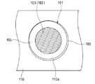
従来から、CD、DVD再生装置等に含まれる光学式ピックアップには、レーザーダイオード等から出射した光を回折させ、メインビーム及びサブビームに振り分ける回折光学素子が装着されている。図4に従来の回折光学素子を示す。この回折光学素子101は、アクリル等の樹脂を射出成形することにより製造されたものであり、4〜5mm程度の外径を有する。同図に示すように、回折光学素子101の中央部には、回折格子102を備えた光学機能部103が形成されている。また、光学機能部103の周囲には、フランジ部104が形成されている。
【0003】
回折光学素子101は、光学式ピックアップに設けられたホルダ部110に取り付けられる。この場合、ホルダ部110に形成された取付穴110aに回折光学素子101を挿入し、回折格子102を所定の方向に向けた状態で皿ばね等を介して固定する。回折光学素子101をホルダ部110に取り付けた際には、回折光学素子101の位置ズレを防止するために、フランジ部104の外周面105と、ホルダ部110の取付穴110aの内周面との間に生ずる隙間をできるだけ少なくする必要がある。
【0004】
【発明が解決しようとする課題】
しかしながら、従来の回折光学素子は、上述したように構成されているため、次のような課題をもっていた。すなわち、従来の回折光学素子101をホルダ部110に取り付ける場合、フランジ部104の外径が取付穴110aの内径よりも小さいと、図4に示すように、両者間の隙間が大きくなって位置ズレが発生してしまい、光学式ピックアップの性能の劣化を招く。一方、フランジ部104の外径が取付穴110aの内径よりも大きいと、取付穴110aに挿入できなくなってしまう。従って、従来の回折光学素子は取付性の点で問題を有していた。
【0005】
また、フランジ部104の外周面105の外径を取付穴110aの内径とほぼ一致させるためには、回折光学素子101を製造する際、外周面105の公差をできるだけ小さく設定しなければならない。例えば、外径4〜5mmの回折光学素子では、公差を0.01〜0.03mm程度に設定する必要がある。この場合、外周面105の外径が取付穴110aの内径よりも小さい場合、所定の公差を満足するまで成形金型全体を修正する必要が生じてしまう。また、フランジ部104の外径が取付穴110aの内径よりも大きければ、改めて新しい金型を作らなければならない。これでは、製造コストの増加を招いてしまい、また、製造効率の点においても問題がある。
【0006】
そこで、本発明は、良好な取付性を有し、かつ、低コストで効率よく製造可能な回折光学素子を提供することを目的とする。
【0007】
【課題を解決するための手段】
本発明に係る回折光学素子は、回折格子を備えた光学機能部の周囲にフランジ部を形成してなり、ホルダ部の取付穴に挿入されて固定される回折光学素子において、フランジ部の外周面における少なくとも3ヶ所に形成され、外周面から外方に突出する係合突部を備え、係合突部は、フランジ部の一端面側から他端面側に向かって先細りとなるように概略三角錐形状に形成されており、フランジ部の一端面と他端面との間の所定位置を通り且つフランジ部の中心軸に直交する平面内において、係合突起のそれぞれに外接する円の直径は、取付穴の内径と一致しており、光学機能部、フランジ部及び係合突部は、一体成形されていることを特徴とする。
【0008】
この回折光学素子を光学式ピックアップ等に含まれるホルダ部に装着させた場合、外周面の少なくとも3ヶ所に形成された係合突部とホルダ部の内部側面とが接触することになる。これにより、回折光学素子は3点以上の接触部分を介してホルダ部に保持されるので、取付時のガタつき、位置ズレを防止することができる。また、回折光学素子をホルダ部に精度よく取り付けるために、成形金型の修正が必要になった場合でも、成形金型の係合突部形成部のみを修正すればよく、外周面形成部の修正が不要となることから、金型の修正に要するコスト、時間を削減できる。従って、全体として、製造コストが低減されると共に、製造効率も向上する。
【0009】
更に、この回折光学素子では、ホルダ部の内部側面と接触するのは係合突部のみであることから、回折光学素子の外周面とホルダ部の内部側面との間に空間が形成される、これにより、この空間が緩衝として機能し、回折光学素子に作用する熱等による影響を緩和することができるので、回折光学素子の光学性能を良好な状態に維持することができる。
【0010】
また、係合突部は概略三角錐形状を有すると好ましい。すなわち、係合突部を、ホルダ部に向けて先細りに形成する。このような構成を採用すれば、回折光学素子をホルダ部に押し込むことにより、回折光学素子をホルダ部に固定することが可能となる。
【0011】
【発明の実施の形態】
以下、図面と共に本発明による回折光学素子の好適な実施形態について詳細に説明する。
【0012】
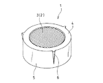
図1は、本発明による回折光学素子を示す斜視図である。同図に示す回折光学素子1は、アクリル等のプラスチック樹脂を、射出成形、トランスファ成形等して製造され、4〜5mmの外径を有する。この回折光学素子1は、CD、DVD再生装置等に含まれる光学式ピックアップ(図示せず)に装着することを主目的としたものである。同図に示すように、回折光学素子1の中央部には、回折格子2を備えた光学機能部3が形成されている。回折格子2は、回折光学素子1の表面及び裏面に形成された微少な凹凸からなり、レーザーダイオード等(図示せず)から出射した光を回折させ、メインビーム及びサブビームに振り分ける。
【0013】
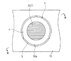
光学機能部3の周囲には、フランジ部4が形成されている。図2に示すように、回折光学素子1を光学式ピックアップに設けられたホルダ部10に取り付ける際、このフランジ部4は、いわゆる基準面として機能する。フランジ部4の外周面5は、円柱面として形成されているが、この外周面5の3ヶ所には、外周面5から外方に突出する係合突部6が設けられている。各係合突部6は、それぞれ等間隔を隔てて、すなわち、中心角120゜おきに形成されている。図2に示すように、この回折光学素子1をホルダ部10に装着させた場合、外周面5の3ヶ所に形成された係合突部6と取付穴10aの内部側面とが接触することになる。これにより、回折光学素子1は、3点の接触部分を介してホルダ部10に保持されるので、取付時のガタつき、位置ズレが防止され、回折光学素子1の取付性が向上する。
【0014】
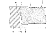
係合突部6は、底面がフランジ部4の上面と面一であり、頂点がフランジ部4の下面側に位置する概略三角錐形状を有する。回折光学素子1を中心軸に直交する平面で切断した場合、この平面と各係合突部6の稜線6aとの交点を結んだ三角形は正三角形となる。この回折光学素子1では、フランジ部4の上面よりも下側の所定位置(例えば、フランジ部4の上面から、回折光学素子1の高さの4分の1程度下方の位置)を通り、中心軸に直交する平面と、各係合突部6の稜線6aとの交点を結んだ正三角形に外接する円の直径が、取付穴10aの内径と一致する。そして、この平面よりも上側では、各係合突部6の稜線6aと中心軸との距離は、取付穴10aの半径より僅かに長くなっている。また、係合突部6の高さ(上下方向の長さ)は、回折光学素子1の高さよりも短く、係合突部6の頂点は、フランジ部4の下面よりも上側に位置する。
【0015】
これにより、回折光学素子1を取付穴10aに真っ直ぐに押し込めば、係合突部6の上部が、図3に示すように弾性変形するので、回折光学素子1をホルダ部10に固定することが可能となる。回折光学素子1を取付穴10aに挿入する際の圧力は、20〜200gfとすると実用上良好な結果が得られる。この場合、回折光学素子1をホルダ部10に固定するための皿ばね等を省略することも可能である。また、各係合突部6は、ホルダ部10に向けて先細りに形成されているので、回折光学素子1を取付穴10aに容易に挿入することができる。
【0016】
また、回折光学素子1をホルダ部10に装着させた場合、外周面5の3ヶ所に形成された係合突部6のみが取付穴10aの内部側面と接触し、回折光学素子1の外周面5は、取付穴10aの内部側面と直接接触しない。従って、回折光学素子1の外周面5と取付穴10aの内部側面との間に空間7が形成される(図2参照)。これにより、回折光学素子1と取付穴10aとの間に形成される空間7が緩衝として機能するので、回折光学素子1に作用する熱等による影響を緩和することができる。
【0017】
すなわち、一般的に、ホルダ部10はダイキャストや耐熱プラスチック等により形成されるため、光学式ピックアップの使用時に、ホルダ部10の温度が上昇することがある。ここで、この回折光学素子1では、ホルダ部10と回折光学素子1との接触部分が係合突部6のみである。従って、外周面5のほぼ全体が取付穴10aの内周面と接触する場合と比較して、ホルダ部10から回折光学素子1に伝わる熱量を減らすことができる。これにより、光学式ピックアップを長時間連続使用しても、回折光学素子1の光学性能は良好な状態に維持される。
【0018】
この回折光学素子1は、図示しない成形金型を用いてアクリル等のプラスチックを射出成形等することにより製造されるが、一旦、回折光学素子1が完成しても、回折光学素子1をホルダ部10に精度よく取り付けるために成形金型の修正が必要になる場合もある。この場合、回折光学素子1は係合突部6を介してホルダ部10に保持されることから、成形金型の係合突部形成部のみを修正すればよく、外周面形成部の修正が不要となる。これにより、金型の修正に要するコスト、時間を削減できる。従って、全体として、製造コストが低減されると共に、製造効率も向上する。
【0019】
なお、上述した回折光学素子1では、外周面5の3ヶ所に係合突部6を形成しているが、これに限られるものではなく、外周面5の4ヶ所、6ヶ所、又は、それ以上の位置に係合突部6を設けてもよい。また、係合突部6の形状も、三角錐形状に限られるものではなく、半円錐形状等に形成してもよい。
【0020】
【発明の効果】
本発明による回折光学素子は、以上説明したように構成されているため、次のような効果を得る。すなわち、フランジ部の外周面に少なくとも3個の係合突部を設け、この係合突部を介して回折光学素子をホルダ部に取り付けるので、回折光学素子の取付性が向上する。また、良好な取付性を有する回折光学素子を低コストで効率よく製造することができる。
【図面の簡単な説明】
【図1】本発明による回折光学素子を示す斜視図である。
【図2】図1の回折光学素子をホルダ部に装着した状態を示す平面図である。
【図3】図2におけるIII−III線についての要部拡大断面図である。
【図4】従来の回折光学素子をホルダ部に装着した状態を示す平面図である。
【符号の説明】
1…回折光学素子、2…回折格子、3…光学機能部、4…フランジ部、5…外周面、6…係合突部。[0001]
BACKGROUND OF THE INVENTION
The present invention relates to a diffractive optical element used for an optical pickup or the like included in a CD or DVD reproducing apparatus.
[0002]
[Prior art]
Conventionally, an optical pickup included in a CD, DVD reproducing apparatus or the like is equipped with a diffractive optical element that diffracts light emitted from a laser diode or the like and distributes the light into a main beam and a sub beam. FIG. 4 shows a conventional diffractive optical element. The diffractive
[0003]
The diffractive
[0004]
[Problems to be solved by the invention]
However, since the conventional diffractive optical element is configured as described above, it has the following problems. That is, when attaching the conventional diffractive
[0005]
In order to make the outer diameter of the outer
[0006]
SUMMARY OF THE INVENTION An object of the present invention is to provide a diffractive optical element that has good mountability and can be manufactured efficiently at low cost.
[0007]
[Means for Solving the Problems]
The diffractive optical element according to the present invention is a diffractive optical element in which a flange portion is formed around an optical function portion provided with a diffraction grating, and is inserted into a mounting hole of a holder portion and fixed. Are formed at at least three locations, and projecting outwardly from the outer peripheral surface, and the engaging projections are substantially triangular pyramids so as to taper from one end surface side to the other end surface side of the flange portion. The diameter of the circle circumscribing each of the engaging protrusions in a plane passing through a predetermined position between one end surface and the other end surface of the flange portion and orthogonal to the central axis of the flange portion The optical function portion, the flange portion, and the engagement protrusion are formed integrally with each other so as to coincide with the inner diameter of the hole.
[0008]
When this diffractive optical element is mounted on a holder part included in an optical pickup or the like, the engagement protrusions formed at at least three locations on the outer peripheral surface come into contact with the inner side surface of the holder part. As a result, the diffractive optical element is held on the holder portion via three or more contact portions, so that it is possible to prevent backlash and displacement during mounting. Further, in order to attach the diffractive optical element to the holder portion with high accuracy, even when it is necessary to correct the molding die, only the engaging projection forming portion of the molding die need be corrected. Since no correction is required, the cost and time required to correct the mold can be reduced. Therefore, as a whole, the manufacturing cost is reduced and the manufacturing efficiency is improved.
[0009]
Furthermore, in this diffractive optical element, since only the engaging protrusions are in contact with the inner side surface of the holder part, a space is formed between the outer peripheral surface of the diffractive optical element and the inner side surface of the holder part. As a result, this space functions as a buffer and the influence of heat or the like acting on the diffractive optical element can be reduced, so that the optical performance of the diffractive optical element can be maintained in a good state.
[0010]
Further, it is preferable that the engaging protrusion has a substantially triangular pyramid shape. That is, the engaging protrusion is formed to be tapered toward the holder portion. If such a structure is employ | adopted, it will become possible to fix a diffractive optical element to a holder part by pushing a diffractive optical element into a holder part.
[0011]
DETAILED DESCRIPTION OF THE INVENTION
Hereinafter, preferred embodiments of a diffractive optical element according to the present invention will be described in detail with reference to the drawings.
[0012]
FIG. 1 is a perspective view showing a diffractive optical element according to the present invention. The diffractive
[0013]
A flange portion 4 is formed around the
[0014]
The
[0015]
As a result, when the diffractive
[0016]
Further, when the diffractive
[0017]
That is, since the
[0018]
The diffractive
[0019]
In the diffractive
[0020]
【The invention's effect】
Since the diffractive optical element according to the present invention is configured as described above, the following effects are obtained. That is, since at least three engaging protrusions are provided on the outer peripheral surface of the flange portion, and the diffractive optical element is attached to the holder portion via the engaging protrusion, the attachment of the diffractive optical element is improved. In addition, a diffractive optical element having good mounting properties can be efficiently manufactured at a low cost.
[Brief description of the drawings]
FIG. 1 is a perspective view showing a diffractive optical element according to the present invention.
FIG. 2 is a plan view showing a state in which the diffractive optical element of FIG. 1 is mounted on a holder portion.
3 is an enlarged cross-sectional view of a main part taken along line III-III in FIG. 2. FIG.
FIG. 4 is a plan view showing a state in which a conventional diffractive optical element is mounted on a holder portion.
[Explanation of symbols]
DESCRIPTION OF
Claims (2)
前記フランジ部の外周面における少なくとも3ヶ所に形成され、前記外周面から外方に突出する係合突部を備え、
前記係合突部は、前記フランジ部の一端面側から他端面側に向かって先細りとなるように概略三角錐形状に形成されており、
前記フランジ部の一端面と他端面との間の所定位置を通り且つ前記フランジ部の中心軸に直交する平面内において、前記係合突起のそれぞれに外接する円の直径は、前記取付穴の内径と一致しており、
前記光学機能部、前記フランジ部及び前記係合突部は、一体成形されていることを特徴とする回折光学素子。In the diffractive optical element formed by forming a flange portion around the optical function portion provided with the diffraction grating, and being inserted and fixed in the mounting hole of the holder portion,
Formed in at least three places on the outer peripheral surface of the flange portion, and provided with an engaging protrusion protruding outward from the outer peripheral surface;
The engagement protrusion is formed in a substantially triangular pyramid shape so as to taper from the one end surface side to the other end surface side of the flange portion,
In a plane perpendicular to the central axis of the predetermined position through and the flange portion between the one end surface and other end surface of the flange portion, the diameter of the circle circumscribing the respective said engagement protrusion, the inside diameter of the mounting hole And
The diffractive optical element, wherein the optical function part, the flange part, and the engagement protrusion are integrally formed.
Priority Applications (2)
| Application Number | Priority Date | Filing Date | Title |
|---|---|---|---|
| JP27126197A JP4040726B2 (en) | 1997-10-03 | 1997-10-03 | Diffractive optical element |
| US09/161,744 US6088160A (en) | 1997-10-03 | 1998-09-29 | Diffractive optical element |
Applications Claiming Priority (1)
| Application Number | Priority Date | Filing Date | Title |
|---|---|---|---|
| JP27126197A JP4040726B2 (en) | 1997-10-03 | 1997-10-03 | Diffractive optical element |
Publications (2)
| Publication Number | Publication Date |
|---|---|
| JPH11109109A JPH11109109A (en) | 1999-04-23 |
| JP4040726B2 true JP4040726B2 (en) | 2008-01-30 |
Family
ID=17497621
Family Applications (1)
| Application Number | Title | Priority Date | Filing Date |
|---|---|---|---|
| JP27126197A Expired - Fee Related JP4040726B2 (en) | 1997-10-03 | 1997-10-03 | Diffractive optical element |
Country Status (2)
| Country | Link |
|---|---|
| US (1) | US6088160A (en) |
| JP (1) | JP4040726B2 (en) |
Families Citing this family (15)
| Publication number | Priority date | Publication date | Assignee | Title |
|---|---|---|---|---|
| US6292311B1 (en) * | 1999-10-13 | 2001-09-18 | Hewlett-Packard Company | Method and apparatus for centering a lens within an optical bore sleeve |
| US6205293B1 (en) * | 2000-02-16 | 2001-03-20 | Eastman Kodak Company | Rotary engaging lens and mount assemblage |
| US7597711B2 (en) * | 2004-01-26 | 2009-10-06 | Arbor Surgical Technologies, Inc. | Heart valve assembly with slidable coupling connections |
| JP4773756B2 (en) * | 2005-07-07 | 2011-09-14 | 富士フイルム株式会社 | Mirror frame, lens frame manufacturing method, lens frame molding die, and lens positioning method |
| EP1816493A1 (en) * | 2006-02-07 | 2007-08-08 | ETH Zürich | Tunable diffraction grating |
| EP1876484B1 (en) * | 2006-10-20 | 2015-09-30 | Fujifilm Corporation | Lens frame, manufacturing method of the same, metal mold for molding the same, and lense positioning method |
| EP2270567A4 (en) * | 2008-04-16 | 2014-08-06 | Komatsulite Mfg Co Ltd | Imaging lens unit |
| DE102008057356A1 (en) * | 2008-11-14 | 2010-05-20 | Osram Gesellschaft mit beschränkter Haftung | Optical lens and manufacturing method for an optical lens |
| US8699141B2 (en) | 2009-03-13 | 2014-04-15 | Knowles Electronics, Llc | Lens assembly apparatus and method |
| US8659835B2 (en) * | 2009-03-13 | 2014-02-25 | Optotune Ag | Lens systems and method |
| DE102010017977A1 (en) * | 2010-04-23 | 2011-10-27 | Conti Temic Microelectronic Gmbh | Optical device with optical module and carrier housing |
| USD684617S1 (en) * | 2011-11-28 | 2013-06-18 | Micro World Corp. | Optical device |
| DE102014211832A1 (en) * | 2014-06-20 | 2015-12-24 | Robert Bosch Gmbh | Holder for a lens and an image sensor, lens, imager module, camera and driver assistance system |
| US9863809B2 (en) * | 2015-08-31 | 2018-01-09 | Mettler-Toledo Gmbh | Spectrograph |
| WO2020239480A1 (en) * | 2019-05-31 | 2020-12-03 | Carl Zeiss Jena Gmbh | Method for adjusting the holder of an optical element held in a holder, optical component and optical assembly |
Family Cites Families (2)
| Publication number | Priority date | Publication date | Assignee | Title |
|---|---|---|---|---|
| JP3062760B2 (en) * | 1989-03-14 | 2000-07-12 | コニカ株式会社 | Compound lens |
| JP3627252B2 (en) * | 1994-03-30 | 2005-03-09 | ソニー株式会社 | Projection television lens assembly and projection television apparatus |
-
1997
- 1997-10-03 JP JP27126197A patent/JP4040726B2/en not_active Expired - Fee Related
-
1998
- 1998-09-29 US US09/161,744 patent/US6088160A/en not_active Expired - Lifetime
Also Published As
| Publication number | Publication date |
|---|---|
| US6088160A (en) | 2000-07-11 |
| JPH11109109A (en) | 1999-04-23 |
Similar Documents
| Publication | Publication Date | Title |
|---|---|---|
| JP4040726B2 (en) | Diffractive optical element | |
| US7151640B2 (en) | Molded lens having an outer circumference and first and second optical surfaces with cut off peripheral portions, and molding die for the molded lens | |
| JP4043560B2 (en) | Optical lens | |
| US7286448B2 (en) | Actuator for use in pickup device in reducing lens distortion | |
| JP2806422B2 (en) | Condensing lens for optical disc | |
| JP2861862B2 (en) | Collimating device having a plastic collimating lens | |
| EP0397171B1 (en) | Optical device | |
| JP3841902B2 (en) | Vehicle lamp | |
| US7897242B2 (en) | Injection molded article | |
| US6250790B1 (en) | Motor vehicle headlight with a transverse lamp, having an improved lamp mount | |
| US6356526B1 (en) | Optical device | |
| JP2002365511A (en) | Laser beam projecting unit | |
| JP3351493B2 (en) | Two-axis actuator and lens fixing method | |
| JPH0341483Y2 (en) | ||
| JPH058573Y2 (en) | ||
| JP2004205774A (en) | Optical unit | |
| US7088754B2 (en) | Semiconductor laser device and optical pickup device | |
| JPS6278510A (en) | Optical element holding frame | |
| JP2000111709A (en) | Optical component | |
| JP3091613U (en) | Heat dissipation structure of laser diode | |
| JPH09297275A (en) | Optical device | |
| JPH04253009A (en) | Synthetic resin lens for scanning optical system | |
| JPH11191237A (en) | Optical pickup | |
| JP2859641B2 (en) | Long roof mirror lens array | |
| WO2018164179A1 (en) | Lamp for vehicle |
Legal Events
| Date | Code | Title | Description |
|---|---|---|---|
| A621 | Written request for application examination |
Free format text: JAPANESE INTERMEDIATE CODE: A621 Effective date: 20040426 |
|
| A131 | Notification of reasons for refusal |
Free format text: JAPANESE INTERMEDIATE CODE: A131 Effective date: 20070508 |
|
| A521 | Request for written amendment filed |
Free format text: JAPANESE INTERMEDIATE CODE: A523 Effective date: 20070705 |
|
| A131 | Notification of reasons for refusal |
Free format text: JAPANESE INTERMEDIATE CODE: A131 Effective date: 20070814 |
|
| A521 | Request for written amendment filed |
Free format text: JAPANESE INTERMEDIATE CODE: A523 Effective date: 20071002 |
|
| TRDD | Decision of grant or rejection written | ||
| A01 | Written decision to grant a patent or to grant a registration (utility model) |
Free format text: JAPANESE INTERMEDIATE CODE: A01 Effective date: 20071106 |
|
| A61 | First payment of annual fees (during grant procedure) |
Free format text: JAPANESE INTERMEDIATE CODE: A61 Effective date: 20071108 |
|
| FPAY | Renewal fee payment (event date is renewal date of database) |
Free format text: PAYMENT UNTIL: 20101116 Year of fee payment: 3 |
|
| R150 | Certificate of patent or registration of utility model |
Free format text: JAPANESE INTERMEDIATE CODE: R150 |
|
| FPAY | Renewal fee payment (event date is renewal date of database) |
Free format text: PAYMENT UNTIL: 20101116 Year of fee payment: 3 |
|
| S111 | Request for change of ownership or part of ownership |
Free format text: JAPANESE INTERMEDIATE CODE: R313113 |
|
| FPAY | Renewal fee payment (event date is renewal date of database) |
Free format text: PAYMENT UNTIL: 20101116 Year of fee payment: 3 |
|
| R350 | Written notification of registration of transfer |
Free format text: JAPANESE INTERMEDIATE CODE: R350 |
|
| FPAY | Renewal fee payment (event date is renewal date of database) |
Free format text: PAYMENT UNTIL: 20111116 Year of fee payment: 4 |
|
| FPAY | Renewal fee payment (event date is renewal date of database) |
Free format text: PAYMENT UNTIL: 20121116 Year of fee payment: 5 |
|
| FPAY | Renewal fee payment (event date is renewal date of database) |
Free format text: PAYMENT UNTIL: 20121116 Year of fee payment: 5 |
|
| FPAY | Renewal fee payment (event date is renewal date of database) |
Free format text: PAYMENT UNTIL: 20131116 Year of fee payment: 6 |
|
| LAPS | Cancellation because of no payment of annual fees |