JP4036572B2 - Manufacturing method of electron emission source - Google Patents
Manufacturing method of electron emission source Download PDFInfo
- Publication number
- JP4036572B2 JP4036572B2 JP20256299A JP20256299A JP4036572B2 JP 4036572 B2 JP4036572 B2 JP 4036572B2 JP 20256299 A JP20256299 A JP 20256299A JP 20256299 A JP20256299 A JP 20256299A JP 4036572 B2 JP4036572 B2 JP 4036572B2
- Authority
- JP
- Japan
- Prior art keywords
- electron emission
- emitter
- emission source
- cathode conductor
- etching
- Prior art date
- Legal status (The legal status is an assumption and is not a legal conclusion. Google has not performed a legal analysis and makes no representation as to the accuracy of the status listed.)
- Expired - Fee Related
Links
Images


Classifications
-
- B—PERFORMING OPERATIONS; TRANSPORTING
- B82—NANOTECHNOLOGY
- B82Y—SPECIFIC USES OR APPLICATIONS OF NANOSTRUCTURES; MEASUREMENT OR ANALYSIS OF NANOSTRUCTURES; MANUFACTURE OR TREATMENT OF NANOSTRUCTURES
- B82Y30/00—Nanotechnology for materials or surface science, e.g. nanocomposites
Description
【0001】
【発明の属する技術分野】
本発明は、電子を放出する電子放出源の製造方法、これによって製造した電子放出源及び前記電子放出源を使用した蛍光発光型表示器に関する。
【0002】
【従来の技術】
従来から、カソード導体とゲート電極(引き出し電極)間に、電子を放出する電子放出材料によって形成されたエミッタを配設し、前記カソード導体とゲート電極間に電圧を印加することにより前記エミッタから電子を放出する電子放出源が一部で実用化され又、研究が進められている。
【0003】
電界の作用によって電子を放出する電界電子放出源は、金属または半導体等の表面の印加電界を109V/m程度にするとトンネル効果により障壁を通過して常温でも真空中に電子放出が行われる現象であり、熱エネルギーを利用する電子源(熱電子放出源)に比べ、省エネルギーで長寿命化が可能等、多くの優れた点を有している。エミッタ材料としては、シリコン等の半導体、タングステン、モリブデンなどの金属、ダイヤモンドライクカーボン(DLC;Diamond-Like Carbon)等がある。
【0004】
エミッタに印加される電界強度によって、その引き出し電流が決定されるため、低電圧駆動で高効率な電子放出源を構成するためには、鋭利な先端を持つエミッタを使用する必要があるため、前記半導体や金属等を使用してエミッタを形成する場合には、電子放出部の先端を鋭利な針状に加工することが必要となる。
しかしながら、前記半導体や金属等の先端を鋭利な針状に加工することは容易でなく又、大規模な装置が必要になるため極めて高価になるという問題がある。
【0005】
以上の点から、最近、カーボンナノチューブが電子放出材料として注目されつつある。カーボンナノチューブはその外径が1〜数10nmと非常に小さい線状のカーボン材料であり、形状的には電界集中が起きやすく低電圧で電子放出を行わせるのに十分な構造形態を持ち、その材料であるカーボンは化学的に安定、機械的にも強靱であるという特徴を持つため、エミッタに適した材料である。
【0006】
例えば、カーボンナノチューブを利用した電子放出源として、特開平10−31954号公報に開示された電子放出源がある。前記電子放出源は、カーボンナノチューブを含むペースト材料をカソード導体上、あるいは前記カソード導体上に被着された抵抗層上に印刷後、焼成し、その上方にリブ状のゲート電極を配置した構造のものがあり、前記カソード導体とゲート電極間に電圧を印加することにより、電子を放出させることができる。
また、前記電子放出源を蛍光発光型表示器の電子放出源として使用する場合には、前記電子放出源に対向するように蛍光体を被着したアノード電極を設けて、これらを真空気密容器内に配設することによって蛍光発光型表示器を形成する。かかる構成とすることにより、前記ゲート電極及びアノード電極を所定の正電位に駆動することによって、前記カーボンナノチューブから放出される電子により前記蛍光体を励起し、発光表示させることができる。
【0007】
【発明が解決しようとする課題】
前記公報に記載された電子放出源においては、カーボンナノチューブを含むカーボン材料をペースト化し、このペースト材料を印刷形成後、乾燥、焼成するにすぎないため、前記カーボン材料をペースト化するための溶剤に含まれる成分が焼成後も残存し、これがカーボンナノチューブの表面を覆った状態でエミッタが形成されるため、エミッタの仕事関数が高くなってしまう。よって、低電圧での電子放出が困難になり又、電子放出効率が低いという問題があった。また、電子放出源として微細で複雑な構造の電子放出源の洗浄が困難であった。
【0008】
また、カーボンナノチューブ以外にも微少なカーボン材料としてフラーレン、ナノパーティクル、ナノカプセルあるいはカーボンナノホーン等が注目されているが、これらのペースト材料を用いてエミッタを形成した場合にも、前記同様に、低電圧で高効率に電子放出を生じさせることが困難であるという問題があった。
したがって、前記方法で得られた電子放出源を蛍光発光型表示器に使用した場合に、低電圧の駆動では高輝度な発光表示を得ることが困難であるという問題があった。
【0009】
本発明は、前記問題点に鑑み成されたもので、カーボンナノチューブ、フラーレン、ナノパーティクル、ナノカプセル及びカーボンナノホーンの中の少なくとも一つを有するカーボン材料を用いて、低電圧駆動で高効率な電子放出を可能にすることを課題としている。
【0010】
【課題を解決するための手段】
本発明によれば、カソード導体とゲート電極間にエミッタを配設し、前記カソード導体とゲート電極間に電圧を印加することにより前記エミッタから電子を放出する電子放出源の製造方法において、絶縁基板にカソード導体を被着する工程と、前記カソード導体にカーボンナノチューブ、フラーレン、ナノパーティクル、ナノカプセル及びカーボンナノホーンの中の少なくとも一つを含むペースト材料を被着してエミッタを形成する工程と、前記エミッタの表面をドライエッチングによりエッチング処理する工程と、前記エミッタから離間する位置にゲート電極を形成する工程とを備えて成ることを特徴とする電子放出源の製造方法が提供される。
【0011】
また、本発明によれば、カソード導体とゲート電極間にエミッタを配設し、前記カソード導体とゲート電極間に電圧を印加することにより前記エミッタから電子を放出する電子放出源の製造方法において、絶縁基板にカソード導体を被着する工程と、前記カソード導体に抵抗層を被着する工程と、前記抵抗層にカーボンナノチューブ、フラーレン、ナノパーティクル、ナノカプセル及びカーボンナノホーンの中の少なくとも一つを含むペースト材料を被着してエミッタを形成する工程と、前記エミッタの表面をドライエッチングによりエッチング処理する工程と、前記エミッタから離間する位置にゲート電極を形成する工程とを備えて成ることを特徴とする電子放出源の製造方法が提供される。
【0012】
ここで、前記ドライエッチングとして、H2又はO2を含むエッチングガス、あるいは、CxHy系ガス又はCxHyFz系ガスを含むエッチングガスを使用した反応性イオンエッチングを使用してもよい。
また、本発明によれば、カソード導体とゲート電極間にエミッタを配設し、前記カソード導体とゲート電極間に電圧を印加することにより前記エミッタから電子を放出する電子放出源において、前記エミッタは、カーボンナノチューブ、フラーレン、ナノパーティクル、ナノカプセル及びカーボンナノホーンの中の少なくとも一つを有するカーボン材料を、直接又は抵抗層を介して前記カソード導体に被着すると共に、前記カーボン材料をドライエッチングによってエッチング処理することにより形成したことを特徴とする電子放出源が提供される。
【0013】
さらに、本発明によれば、電子放出源及び蛍光体が被着されたアノード電極を真空気密容器内に配設し、前記電子放出源から放出される電子を前記蛍光体に射突させることにより発光表示を行う蛍光発光型表示器において、前記電子放出源電子放出源を使用したことを特徴とする蛍光発光型表示器が提供される。
【0014】
【発明の実施の形態】
以下、図面を用いて、本発明の実施の形態について説明する。尚、各図において同一部分には同一符号を付している。
図1乃至図3は、本発明の実施の形態に係る電子放出源の製造方法を説明するための側断面図である。
【0015】
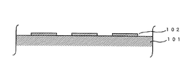
先ず、図1において、硼珪酸ガラス等の絶縁基板101上に、銀ペーストをスクリーン印刷により被着し、焼成することによって、カソード導体102を約5μm程度の膜厚に被着形成する。
次に、図2に示すように、カソード導体102の上部に、電子放出の安定化や電極短絡時の過電流防止を図るための抵抗体材料をスクリーン印刷により約5μm程度の膜厚に被着し、焼成することによって抵抗層201被着形成する。抵抗層201の材料としては、RuO2系の抵抗体材料等が使用できる。
【0016】
次に、カーボンナノチューブを含むペースト材料を、図3に示すように、スクリーン印刷により抵抗層201上に塗布して、カーボンナノチューブを含むエミッタ301を約10μm程度の膜厚に形成する。
尚、カーボンナノチューブを含むペースト材料としては、アーク放電法によって生成したカーボンナノチューブを含むカーボン材料を、エチルセルローズをテルピオネールに溶解した溶液に、超音波等によって良く分散したものを使用することができる。また、抵抗層201との固着強度を増すために、焼成後にも残る無機系の接着剤(ガラス系、金属アルコキシド等)を適宜添加することができる。
【0017】
次に、所定温度(例えば、約100度C程度)まで昇温してペースト状のエミッタ301を乾燥させた後、所定温度(例えば、約500度C程度)の大気中下で焼成することにより、絶縁基板101上に、カソード導体102、抵抗層201及びエミッタ301が積層被着されたカソード基板302が完成する。
【0018】
次に、前記のようにして形成されたカソード基板302を反応性イオンエッチング(RIE)によりエッチング処理する。
図6は、カソード基板301にRIE処理を施すための装置を示す図で、チャンバ601内に設けられた上部電極602に対向するように、下部電極603上にカソード基板302を配置し、図示しないガス注入、排出口を通してエッチングガスを注入、排出することによってエッチングガスを供給すると共に、接地された上部電極602と下部電極603との間に、高周波電源604から高周波(例えば13.56MHz)電力を供給する。これにより、カソード基板302のエミッタ301の表面をエッチング処理する。
【0019】
ここで、エッチングガスとして、例えば、H2又はO2を含むエッチングガス、あるいは、CHF3、CF4、C2F6、C3F8、C5F12等のCxHy系又はCxHyFz系ガスを含むエッチングガス等が使用できる。
前記エッチング処理により、エミッタ301のカーボンナノチューブの表面に被着した溶媒成分等が除去され、エミッタ301のカーボンナノチューブ自体がエミッタ301の表面に露出する。
【0020】
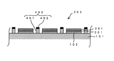
次に、図4に示すように、カソード基板302上で各エミッタ301間の凹部内に、ガラス製絶縁層(リブ)401を約40μm程度の厚みに形成すると共に、該絶縁性リブ401上に約5μm程度の膜厚のゲート電極402を積層被着することにより、リブ状ゲート電極403を形成し、これにより電界放出型の電子放出源が完成する。
尚、リブ状ゲート電極403の形成方法としては、例えば、転写用基板(図示せず)上に、ゲート電極402を形成した後、ゲート電極402上に絶縁性リブ401を積層形成し、さらに絶縁性リブ401上に接着剤(図示せず)を積層被着し、これらを、図4に示す位置に位置合わせを行って転写するようにしてもよい。
【0021】
このようにして得られた電子放出源においては、カソード導体102とゲート電極402間に所定の電圧を印加することにより、エミッタ301の露出したカーボンナノチューブに電界の集中が生じる。したがって、電子放出の開始電圧が低くなり、低電圧で高効率に電子放出を生じさせることが可能になる。また、抵抗層201の存在により、電子放出の安定化や、ゲート電極402とエミッタ301とが短絡した際の過電流の防止が図り得る。
【0022】
尚、本実施の形態においては、エミッタ301表面のエッチング処理は、リブ状ゲート電極403を形成する前に行うようにしたが、リブ状ゲート電極403を形成した後に行うようにしてもよい。
また、エッチング処理は、RIEを使用したが、プラズマエッチングやスパッタエッチング等、各種のドライエッチングが使用できる。
さらに、ゲート電極をリブ状のゲート電極によって形成したが、メッシュ状ゲート電極等、他の構造のゲート電極を使用することもできる。
また、電子放出の安定化や電極短絡時の過電流防止が特に必要とされない場合や、他の構造によって実現できる場合等には、抵抗層201は不要である。この場合、エミッタ301はカソード導体102に直接被着形成されることになる。
【0023】
また、エミッタ301の材料としてカーボンナノチューブを含むカーボン材料を使用したが、フラーレン、ナノパーティクル、ナノカプセルあるいはカーボンナノホーンを含むカーボン材料も使用することが可能である。即ち、エミッタ301の材料として、カーボンナノチューブ、フラーレン、ナノパーティクル、ナノカプセル及びカーボンナノホーンの中、少なくとも一つを有するカーボン材料を含むペースト材料を使用することが可能である。
【0024】
次に、前記電子放出源を使用して、蛍光発光型表示器を形成する。図5は、本発明の実施の形態に係る蛍光発光型表示器の一部切欠き側面図であり、前記の如くして製造した電子放出源を使用した例である。図5において、蛍光発光型表示器は、硼珪酸ガラスによって形成された背面基板としての絶縁基板101、硼珪酸ガラスによって形成された前面基板としての透光性の絶縁基板501、及び、絶縁基板101、501の周囲を封着するシールガラス504とを有し、その内部が真空状態に保持された真空気密容器を備えている。
【0025】
また、前述したように、絶縁基板101の内面上には、カソード導体102、カソード導体102に連続して被着形成された抵抗層201、抵抗層201に連続して被着形成されたエミッタ301が積層被着されている。
さらに、絶縁基板101の内面上にはエミッタ301間の凹部内に、絶縁性リブ401及びゲート電極402が積層されたリブ状ゲート電極403が被着形成されている。
一方、絶縁基板501の内面上には、アノード電極502及びアノード電極502に被着された蛍光体503が積層配設されている。
【0026】
尚、文字やグラフィック等を表示する形式の蛍光発光型表示器の場合には、カソード導体102、アノード電極502及びゲート電極402は、各々、マトリクス状に形成する、あるいは、特定の電極をベタ状に形成して他の電極をマトリクス状に形成する等、適宜目的に応じたパターンに形成する。また、大画面表示装置の画素用発光素子として使用する蛍光発光型表示器の場合にも、前記各電極のパターンを適宜選定して形成する。
【0027】
上記構成の蛍光発光型表示器において、カソード導体102、ゲート電極402及びアノード電極502に所定電圧の駆動信号を供給することにより蛍光体503が発光し、各電極の形成パターンや駆動信号に応じて、文字やグラフィック等の発光表示、あるいは発光素子としての発光表示を行わせることができる。
このとき、エミッタ301の表面に露出したカーボンナノチューブに電界集中が生じるため、低電圧駆動により、高輝度で高品位な発光表示を得ることが可能になる。
【0028】
以上述べたように本発明の実施の形態に係る電子放出源の製造方法は、カソード導体とゲート電極間にエミッタを配設し、前記カソード導体とゲート電極間に電圧を印加することにより前記エミッタから電子を放出する電子放出源の製造方法において、硼珪酸ガラス等の絶縁基板101に銀やアルミニウム等のカソード導体102を被着する工程と、カーボンナノチューブ、フラーレン、ナノパーティクル、ナノカプセル及びカーボンナノホーンの中の少なくとも一つを有するカーボン材料を電子放出材料として使用し該電子放出材料を含むペースト材料を前記カソード導体に被着してエミッタ301を形成する工程と、エミッタ301を焼成する工程と、前記焼成されたエミッタ301の表面をRIE等のドライエッチングによりエッチング処理する工程と、エミッタ301から離間した位置にゲート電極(例えば、リブ状あるいはメッシュ状のゲート電極)402を形成する工程とを備えて成ることを特徴としている。したがって、前記カーボン材料の表面に被着した溶媒成分等が除去されて、カーボン材料であるカーボンナノチューブ、フラーレン、ナノパーティクル、ナノカプセルあるいはカーボンナノホーン自身が露出し、前記露出したカーボン材料に電界集中が生じるため、低電圧で高効率に電子放出を生じる電子放出源を製造することが可能になる。
【0029】
また、前記製造工程中、カソード導体102を被着する工程とエミッタ301を形成する工程の間に、RuO2系の抵抗材料等によって形成した抵抗層201をカソード導体102に被着する工程を付加するようにしてもよい。即ち、絶縁基板101上にカソード導体102を被着する工程と、カソード導体102に抵抗層201を被着する工程と、抵抗層201にカーボンナノチューブ、フラーレン、ナノパーティクル、ナノカプセル及びカーボンナノホーンの中の少なくとも一つを有するカーボン材料を含むペースト材料を被着してエミッタ301を形成する工程とを備えるようにしてもよい。これにより、前記のように低電圧で高効率に電子放出を生じる電子放出源を製造することが可能になるだけでなく、電子放出の安定化や電極短絡時の過電流防止が可能な電子放出源の製造方法が提供される。
【0030】
また、本発明の実施の形態によれば、カソード導体102とゲート電極402間にエミッタ301を配設し、カソード導体102とゲート電極402間に電圧を印加することによりエミッタ301から電子を放出する電子放出源において、エミッタ301は、カーボンナノチューブ、フラーレン、ナノパーティクル、ナノカプセル及びカーボンナノホーンの中の少なくとも一つを有するカーボン材料によって形成されると共に、直接又は抵抗層201を介してカソード導体102に積層被着されて成り、前記カーボン材料はドライエッチングによってエッチング処理されていることを特徴とする電子放出源が提供される。したがって、低電圧で高効率に電子放出を発生することが可能になり又、電子放出の安定化や電極短絡時の過電流防止が可能になる。
【0031】
さらに本発明の実施の形態によれば、蛍光表示管や蛍光発光管等、電子放出源、蛍光体及び前記蛍光体が被着されたアノード電極を真空気密容器内に配設し、前記電子放出源から放出される電子を前記蛍光体に射突させることにより発光表示を行う蛍光発光型表示器において、電子放出源として、前記のようにして得られた電子放出源を使用することにより、低電圧駆動により、高輝度で高品位な発光表示を得ることが可能になる。
【0032】
尚、前記実施の形態においては、カソード導体102に対してゲート電極402を上方に配設する立体構造の電子放出源の例で説明したが、カソード導体とゲート電極の双方を絶縁基板上の同一平面上に配設することにより、平面的な電子放出源を構成することも可能である。
【0033】
【実施例】
図7は本発明の実施例に係る電子放出源の特性評価を行うための装置を示す側断面図で、図8は本実施例の特性図である。
図7で使用した電子放出源はカソード電極とエミッタ間の抵抗層を有しない構造の電子放出源であり、真空外囲器701を構成する一方の絶縁基板101内面にはカソード導体102及びエミッタ301が積層形成され、他方の基板702内面には、エミッタ301に対向してアノード電極502が被着されている。エミッタ301は、カーボンナノチューブを含むカーボン材料によって形成されている。
【0034】
また、カソード導体102とアノード電極502の間に、直流電源703及び電流計704の直列回路が接続されている。
カソード導体102とアノード導体502の距離は200μmで、カソード導体102及びエミッタ301の大きさは1mm×1mmの正方形状に形成されている。
【0035】
尚、エミッタ301のエッチング処理方法としては図6の装置を用いたRIE処理を行い、エッチング条件としては、(1)エッチングガスがO2の場合は、ガス流量が50sccm、交流電源604の出力が160W、チャンバ601内の圧力が5Pa、エッチング時間が120secであり、又、(2)エッチングガスがCHF3の場合は、ガス流量が80sccm、交流電源604の出力が160W、チャンバ601内の圧力が5Pa、エッチング時間が120secで行った。
【0036】
図8において、エミッタ301の放出電流Ieと直流電源703の出力電圧Vg(V)のI−V特性から明らかなように、エッチングガスとしてCHF3を用いてエッチング処理した場合の方が、エッチング処理しない場合(未処理)よりも、低電圧で大きな電流が得られた。また、エッチングガスとしてO2を用いた場合には、さらに低電圧で大きな電流が得られ、電子放出特性がより向上していることがわかる。
【0037】
【発明の効果】
本発明によれば、低電圧で高効率な電子放出源の製造方法を提供することが可能になる。
これにより、電子放出特性の優れた電子放出源を提供することが可能になる。また、低電圧駆動が可能で、高輝度で高品位な蛍光発光型表示器を提供することが可能になる。
【図面の簡単な説明】
【図1】本発明の実施の形態に係る電子放出源の製造方法を説明するための側断面図で、絶縁基板にカソード導体を被着する工程を示す図である。
【図2】本発明の実施の形態に係る電子放出源の製造方法を説明するための側断面図で、カソード基板に抵抗層を被着する工程を示す図である。
【図3】本発明の実施の形態に係る電子放出源の製造方法を説明するための側断面図で、抵抗層にエミッタを被着する工程を示す図である。
【図4】本発明の実施の形態に係る電子放出源の製造方法を説明するための側断面図で、ゲート電極を被着する工程を示す図である。
【図5】本発明の実施の形態に係る蛍光発光型表示器の一部切欠き側面図である。
【図6】本発明の実施の形態に係る電子放出源の製造方法におけるエッチング処理工程を説明するための図である。
【図7】本発明の実施例に係る電子放出源の特性を測定するための装置を示す図である。
【図8】本発明の実施例に係る電子放出源の特性図である。
【符号の説明】
101・・・真空気密容器を構成する前面基板としての絶縁基板
102・・・カソード導体
201・・・抵抗層
301・・・エミッタ
302・・・カソード基板
401・・・リブ
402・・・ゲート電極
501・・・真空気密容器を構成する背面基板としての絶縁基板
502・・・アノード電極
503・・・蛍光体
504・・・真空気密容器を構成するシールガラス[0001]
BACKGROUND OF THE INVENTION
The present invention relates to a method of manufacturing an electron emission source that emits electrons, an electron emission source manufactured by the method, and a fluorescent display using the electron emission source.
[0002]
[Prior art]
Conventionally, an emitter formed of an electron emitting material that emits electrons is disposed between a cathode conductor and a gate electrode (extraction electrode), and a voltage is applied between the cathode conductor and the gate electrode to thereby generate electrons from the emitter. Some electron emission sources that emit light have been put into practical use and are being studied.
[0003]
Field electron emission source for emitting electrons by the action of the electric field, electrons are emitted into a vacuum even at room temperature the applied field of the metal or the surface of a semiconductor such as through the barrier by which the tunnel effect to about 10 9 V / m It is a phenomenon and has many excellent points such as energy saving and longer life compared with an electron source (thermal electron emission source) using thermal energy. Examples of the emitter material include semiconductors such as silicon, metals such as tungsten and molybdenum, diamond-like carbon (DLC), and the like.
[0004]
Since the extraction current is determined by the electric field strength applied to the emitter, it is necessary to use an emitter having a sharp tip in order to construct a high-efficiency electron emission source driven at a low voltage. When an emitter is formed using a semiconductor, metal, or the like, it is necessary to process the tip of the electron emission portion into a sharp needle shape.
However, it is not easy to process the tip of the semiconductor, metal or the like into a sharp needle shape, and there is a problem that a large-scale device is required, which makes it extremely expensive.
[0005]
In view of the above, carbon nanotubes are recently attracting attention as electron emission materials. A carbon nanotube is a linear carbon material with an outer diameter of 1 to several tens of nanometers, and its shape is easy to cause electric field concentration and has a sufficient structure to allow electron emission at a low voltage. Since carbon, which is a material, is characterized by being chemically stable and mechanically strong, it is a material suitable for an emitter.
[0006]
For example, as an electron emission source using carbon nanotubes, there is an electron emission source disclosed in Japanese Patent Application Laid-Open No. 10-31954. The electron emission source has a structure in which a paste material containing carbon nanotubes is printed on a cathode conductor or a resistance layer deposited on the cathode conductor and then fired, and a rib-like gate electrode is disposed above the paste material. There are some, and electrons can be emitted by applying a voltage between the cathode conductor and the gate electrode.
In addition, when the electron emission source is used as an electron emission source of a fluorescent light emitting display, an anode electrode coated with a phosphor is provided so as to face the electron emission source, and these are disposed in a vacuum hermetic container. A fluorescent light-emitting display is formed by disposing in the above. By adopting such a configuration, the phosphor is excited by electrons emitted from the carbon nanotubes by driving the gate electrode and the anode electrode to a predetermined positive potential, and light emission display can be performed.
[0007]
[Problems to be solved by the invention]
In the electron emission source described in the above publication, a carbon material containing carbon nanotubes is made into a paste, and this paste material is merely dried and fired after printing, so that it becomes a solvent for pasting the carbon material. The contained component remains after firing, and the emitter is formed in a state where it covers the surface of the carbon nanotube, so that the work function of the emitter is increased. As a result, it is difficult to emit electrons at a low voltage, and the electron emission efficiency is low. In addition, it is difficult to clean an electron emission source having a fine and complicated structure as an electron emission source.
[0008]
In addition to carbon nanotubes, fullerenes, nanoparticles, nanocapsules, carbon nanohorns, and the like are attracting attention as minute carbon materials. However, when emitters are formed using these paste materials, they are low in the same manner as described above. There is a problem that it is difficult to cause electron emission with high efficiency at a voltage.
Therefore, when the electron emission source obtained by the above method is used for a fluorescent light emitting display, there is a problem that it is difficult to obtain a high luminance light emitting display by driving at a low voltage.
[0009]
The present invention has been made in view of the above problems, and uses a carbon material having at least one of carbon nanotubes, fullerenes, nanoparticles, nanocapsules, and carbon nanohorns, and is a low-voltage driven and highly efficient electron. The issue is to enable release.
[0010]
[Means for Solving the Problems]
According to the present invention, an insulating substrate is provided in a method of manufacturing an electron emission source in which an emitter is disposed between a cathode conductor and a gate electrode, and electrons are emitted from the emitter by applying a voltage between the cathode conductor and the gate electrode. Depositing a cathode conductor on the cathode conductor, depositing a paste material containing at least one of carbon nanotubes, fullerenes, nanoparticles, nanocapsules and carbon nanohorns on the cathode conductor to form an emitter; There is provided a method of manufacturing an electron emission source, comprising: a step of etching a surface of an emitter by dry etching; and a step of forming a gate electrode at a position spaced from the emitter.
[0011]
According to the present invention, in the method of manufacturing an electron emission source, an emitter is disposed between the cathode conductor and the gate electrode, and electrons are emitted from the emitter by applying a voltage between the cathode conductor and the gate electrode. A step of depositing a cathode conductor on an insulating substrate; a step of depositing a resistance layer on the cathode conductor; and the resistance layer includes at least one of carbon nanotubes, fullerenes, nanoparticles, nanocapsules, and carbon nanohorns. A step of forming an emitter by depositing a paste material; a step of etching the surface of the emitter by dry etching; and a step of forming a gate electrode at a position spaced from the emitter. A method for manufacturing an electron emission source is provided.
[0012]
Here, as the dry etching, reactive ion etching using an etching gas containing H 2 or O 2 , or an etching gas containing a C x H y gas or a C x H y F z gas is used. Also good.
According to the present invention, in the electron emission source in which an emitter is disposed between the cathode conductor and the gate electrode and electrons are emitted from the emitter by applying a voltage between the cathode conductor and the gate electrode, A carbon material having at least one of carbon nanotubes, fullerenes, nanoparticles, nanocapsules, and carbon nanohorns is applied to the cathode conductor directly or via a resistance layer, and the carbon material is etched by dry etching. An electron emission source characterized by being formed by processing is provided.
[0013]
Further, according to the present invention, the anode electrode on which the electron emission source and the phosphor are deposited is disposed in the vacuum hermetic container, and the electrons emitted from the electron emission source are projected onto the phosphor. In the fluorescent light-emitting display that performs light-emitting display, there is provided a fluorescent light-emitting display that uses the electron emission source.
[0014]
DETAILED DESCRIPTION OF THE INVENTION
Hereinafter, embodiments of the present invention will be described with reference to the drawings. In the drawings, the same parts are denoted by the same reference numerals.
1 to 3 are side sectional views for explaining a method of manufacturing an electron emission source according to an embodiment of the present invention.
[0015]
First, in FIG. 1, a silver paste is deposited by screen printing on an insulating substrate 101 such as borosilicate glass and fired to form a cathode conductor 102 with a thickness of about 5 μm.
Next, as shown in FIG. 2, a resistor material is deposited on the cathode conductor 102 to a thickness of about 5 μm by screen printing to stabilize electron emission and prevent overcurrent when the electrodes are short-circuited. Then, the
[0016]
Next, as shown in FIG. 3, a paste material containing carbon nanotubes is applied onto the
As the paste material containing carbon nanotubes, a carbon material containing carbon nanotubes produced by an arc discharge method can be used which is well dispersed in a solution of ethyl cellulose dissolved in terpione by ultrasonic waves or the like. . Further, in order to increase the adhesion strength with the
[0017]
Next, the temperature is raised to a predetermined temperature (for example, about 100 ° C.) to dry the paste-like emitter 301, and then fired in the atmosphere at a predetermined temperature (for example, about 500 ° C.). Then, the cathode substrate 302 in which the cathode conductor 102, the
[0018]
Next, the cathode substrate 302 formed as described above is etched by reactive ion etching (RIE).
FIG. 6 is a view showing an apparatus for performing the RIE process on the cathode substrate 301. The cathode substrate 302 is disposed on the lower electrode 603 so as to face the upper electrode 602 provided in the chamber 601, and is not shown. The etching gas is supplied by injecting and exhausting the etching gas through the gas injection and exhaust ports, and high-frequency power (for example, 13.56 MHz) is supplied from the high-frequency power source 604 between the grounded upper electrode 602 and lower electrode 603. Supply. Thereby, the surface of the emitter 301 of the cathode substrate 302 is etched.
[0019]
Here, as an etching gas, for example, an etching gas containing H 2 or O 2 , a C x H y system such as CHF 3 , CF 4 , C 2 F 6 , C 3 F 8 , C 5 F 12, or C etching gas, etc. containing x H y F z based gas can be used.
By the etching process, a solvent component or the like deposited on the surface of the carbon nanotube of the emitter 301 is removed, and the carbon nanotube itself of the emitter 301 is exposed on the surface of the emitter 301.
[0020]
Next, as shown in FIG. 4, a glass insulating layer (rib) 401 is formed to a thickness of about 40 μm in the recess between the emitters 301 on the cathode substrate 302, and on the insulating
As a method for forming the rib-like gate electrode 403, for example, after forming the
[0021]
In the electron emission source thus obtained, application of a predetermined voltage between the cathode conductor 102 and the
[0022]
In this embodiment, the etching process on the surface of the emitter 301 is performed before the rib-shaped gate electrode 403 is formed, but may be performed after the rib-shaped gate electrode 403 is formed.
Moreover, although RIE was used for the etching process, various dry etchings such as plasma etching and sputter etching can be used.
Furthermore, although the gate electrode is formed of a rib-shaped gate electrode, a gate electrode having another structure such as a mesh-shaped gate electrode can also be used.
In addition, the
[0023]
Moreover, although the carbon material containing a carbon nanotube was used as the material of the emitter 301, a carbon material containing fullerene, nanoparticles, nanocapsules, or carbon nanohorns can also be used. That is, as the material of the emitter 301, a paste material containing a carbon material having at least one of carbon nanotubes, fullerenes, nanoparticles, nanocapsules, and carbon nanohorns can be used.
[0024]
Next, a fluorescent light emitting display is formed using the electron emission source. FIG. 5 is a partially cutaway side view of the fluorescent light emitting display according to the embodiment of the present invention, and is an example using the electron emission source manufactured as described above. In FIG. 5, the fluorescent light emitting display includes an insulating substrate 101 as a rear substrate formed of borosilicate glass, a light-transmitting insulating substrate 501 as a front substrate formed of borosilicate glass, and an insulating substrate 101. , And a sealing glass 504 for sealing the periphery of 501, and a vacuum hermetic container in which the inside is maintained in a vacuum state.
[0025]
Further, as described above, on the inner surface of the insulating substrate 101, the cathode conductor 102, the
Further, a rib-like gate electrode 403 in which an insulating
On the other hand, on the inner surface of the insulating substrate 501, an
[0026]
Note that in the case of a fluorescent light-emitting display that displays characters, graphics, etc., the cathode conductor 102, the
[0027]
In the fluorescent light emitting display having the above-described configuration, the phosphor 503 emits light by supplying a drive signal having a predetermined voltage to the cathode conductor 102, the
At this time, since electric field concentration occurs in the carbon nanotube exposed on the surface of the emitter 301, it is possible to obtain a high-luminance and high-quality light-emitting display by low voltage driving.
[0028]
As described above, in the method for manufacturing an electron emission source according to the embodiment of the present invention, an emitter is disposed between a cathode conductor and a gate electrode, and a voltage is applied between the cathode conductor and the gate electrode to thereby form the emitter. In a method for manufacturing an electron emission source that emits electrons from a substrate, a step of depositing a cathode conductor 102 such as silver or aluminum on an insulating substrate 101 such as borosilicate glass, carbon nanotubes, fullerenes, nanoparticles, nanocapsules, and carbon nanohorns Forming a emitter 301 by applying a carbon material having at least one of the above as an electron emission material and applying a paste material containing the electron emission material to the cathode conductor; firing the emitter 301; Etch the surface of the fired emitter 301 by dry etching such as RIE. A step of processing, the gate electrode at a position spaced from the emitter 301 (e.g., a rib-like or mesh-like gate electrode) is characterized by comprising a step of forming a 402. Accordingly, the solvent component or the like deposited on the surface of the carbon material is removed, and the carbon nanotube, fullerene, nanoparticle, nanocapsule, or carbon nanohorn itself that is the carbon material is exposed, and electric field concentration occurs in the exposed carbon material. Therefore, it becomes possible to manufacture an electron emission source that generates electrons with high efficiency at a low voltage.
[0029]
In addition, a step of depositing the
[0030]
Further, according to the embodiment of the present invention, the emitter 301 is disposed between the cathode conductor 102 and the
[0031]
Furthermore, according to an embodiment of the present invention, an electron emission source such as a fluorescent display tube or a fluorescent light emitting tube, a phosphor, and an anode electrode on which the phosphor is deposited are disposed in a vacuum hermetic container, and the electron emission In a fluorescent light emitting display that performs light emission display by causing electrons emitted from a source to collide with the phosphor, by using the electron emission source obtained as described above as an electron emission source, Voltage drive makes it possible to obtain a high-luminance and high-quality light-emitting display.
[0032]
In the above embodiment, an example of a three-dimensional electron emission source in which the
[0033]
【Example】
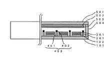
FIG. 7 is a side sectional view showing an apparatus for evaluating the characteristics of an electron emission source according to an embodiment of the present invention, and FIG. 8 is a characteristic diagram of the present embodiment.
The electron emission source used in FIG. 7 is an electron emission source having a structure having no resistance layer between the cathode electrode and the emitter. The cathode conductor 102 and the emitter 301 are formed on the inner surface of one insulating substrate 101 constituting the vacuum envelope 701. The
[0034]
A series circuit of a DC power supply 703 and an
The distance between the cathode conductor 102 and the
[0035]
As the etching method of the emitter 301, RIE processing using the apparatus of FIG. 6 is performed, and the etching conditions are as follows: (1) When the etching gas is O 2 , the gas flow rate is 50 sccm, and the output of the AC power source 604 is 160W, the pressure in the chamber 601 is 5 Pa, the etching time is 120 sec. (2) When the etching gas is CHF 3 , the gas flow rate is 80 sccm, the output of the AC power source 604 is 160 W, and the pressure in the chamber 601 is The etching was performed at 5 Pa and an etching time of 120 seconds.
[0036]
In FIG. 8, as is clear from the IV characteristics of the emission current Ie of the emitter 301 and the output voltage Vg (V) of the DC power supply 703, the etching process is performed using CHF 3 as an etching gas. A larger current was obtained at a lower voltage than when not (untreated). It can also be seen that when O 2 is used as the etching gas, a large current is obtained at a lower voltage, and the electron emission characteristics are further improved.
[0037]
【The invention's effect】
ADVANTAGE OF THE INVENTION According to this invention, it becomes possible to provide the manufacturing method of a low voltage and highly efficient electron emission source.
This makes it possible to provide an electron emission source with excellent electron emission characteristics. In addition, it is possible to provide a fluorescent display which can be driven at a low voltage and has high luminance and high quality.
[Brief description of the drawings]
FIG. 1 is a side sectional view for explaining a method of manufacturing an electron emission source according to an embodiment of the present invention, and is a diagram showing a process of depositing a cathode conductor on an insulating substrate.
FIG. 2 is a side sectional view for explaining the method for manufacturing the electron emission source according to the embodiment of the present invention, and is a view showing a process of depositing a resistance layer on the cathode substrate.
FIG. 3 is a sectional side view for explaining a method of manufacturing an electron emission source according to an embodiment of the present invention, and showing a step of depositing an emitter on a resistance layer.
FIG. 4 is a sectional side view for explaining a method of manufacturing an electron emission source according to an embodiment of the present invention, showing a step of depositing a gate electrode.
FIG. 5 is a partially cutaway side view of a fluorescent light emitting display according to an embodiment of the present invention.
FIG. 6 is a diagram for explaining an etching process in the method for manufacturing an electron emission source according to the embodiment of the present invention.
FIG. 7 is a view showing an apparatus for measuring characteristics of an electron emission source according to an embodiment of the present invention.
FIG. 8 is a characteristic diagram of an electron emission source according to an embodiment of the present invention.
[Explanation of symbols]
DESCRIPTION OF SYMBOLS 101 ... Insulation board | substrate 102 ...
Claims (3)
前記カソード導体にカーボンナノチューブ、フラーレン、ナノパーティクル、ナノカプセル及びカーボンナノホーンの中の少なくとも一つを含むペースト材料を被着してエミッタを形成する工程と、
約500度Cの大気中下で前記エミッタを焼成する工程と、
前記エミッタの表面をドライエッチングによりエッチング処理する工程とを備えて成ることを特徴とする電子放出源の製造方法。Depositing a cathode conductor on an insulating substrate;
Depositing a paste material containing at least one of carbon nanotubes, fullerenes, nanoparticles, nanocapsules and carbon nanohorns on the cathode conductor to form an emitter;
Firing the emitter in an atmosphere of about 500 degrees C;
And a step of etching the surface of the emitter by dry etching.
前記カソード導体に抵抗層を被着する工程と、
前記抵抗層にカーボンナノチューブ、フラーレン、ナノパーティクル、ナノカプセル及びカーボンナノホーンの中の少なくとも一つを含むペースト材料を被着してエミッタを形成する工程と、
約500度Cの大気中下で前記エミッタを焼成する工程と、
前記エミッタの表面をドライエッチングによりエッチング処理する工程とを備えて成ることを特徴とする電子放出源の製造方法。Depositing a cathode conductor on an insulating substrate;
Depositing a resistive layer on the cathode conductor;
Depositing a paste material containing at least one of carbon nanotubes, fullerenes, nanoparticles, nanocapsules, and carbon nanohorns on the resistive layer to form an emitter;
Firing the emitter in an atmosphere of about 500 degrees C;
And a step of etching the surface of the emitter by dry etching.
Priority Applications (1)
| Application Number | Priority Date | Filing Date | Title |
|---|---|---|---|
| JP20256299A JP4036572B2 (en) | 1999-07-16 | 1999-07-16 | Manufacturing method of electron emission source |
Applications Claiming Priority (1)
| Application Number | Priority Date | Filing Date | Title |
|---|---|---|---|
| JP20256299A JP4036572B2 (en) | 1999-07-16 | 1999-07-16 | Manufacturing method of electron emission source |
Publications (3)
| Publication Number | Publication Date |
|---|---|
| JP2001035361A JP2001035361A (en) | 2001-02-09 |
| JP2001035361A5 JP2001035361A5 (en) | 2006-06-08 |
| JP4036572B2 true JP4036572B2 (en) | 2008-01-23 |
Family
ID=16459558
Family Applications (1)
| Application Number | Title | Priority Date | Filing Date |
|---|---|---|---|
| JP20256299A Expired - Fee Related JP4036572B2 (en) | 1999-07-16 | 1999-07-16 | Manufacturing method of electron emission source |
Country Status (1)
| Country | Link |
|---|---|
| JP (1) | JP4036572B2 (en) |
Families Citing this family (10)
| Publication number | Priority date | Publication date | Assignee | Title |
|---|---|---|---|---|
| JP3632682B2 (en) * | 2001-07-18 | 2005-03-23 | ソニー株式会社 | Method for manufacturing electron emitter, method for manufacturing cold cathode field emission device, and method for manufacturing cold cathode field emission display |
| JP2003168355A (en) * | 2001-11-30 | 2003-06-13 | Sony Corp | Manufacturing method of electron emission body, manufacturing method of cold-cathode field electron emission element, and manufacturing method of cold- cathode field electron emission display device |
| JP3432818B1 (en) | 2002-03-07 | 2003-08-04 | 科学技術振興事業団 | Nanohorn carrier and method for producing the same |
| JP2003303540A (en) * | 2002-04-11 | 2003-10-24 | Sony Corp | Field electron emission membrane, field electron emission electrode, and field electron emission display device |
| JP4543604B2 (en) * | 2002-05-20 | 2010-09-15 | ソニー株式会社 | Manufacturing method of electron emission region |
| JP2004178972A (en) * | 2002-11-27 | 2004-06-24 | Sony Corp | Manufacturing method of electron emitting element and display device |
| US7044822B2 (en) * | 2002-12-20 | 2006-05-16 | Samsung Sdi Co., Ltd. | Method of manufacturing a field emission device utilizing the sacrificial layer |
| KR101082440B1 (en) | 2005-10-04 | 2011-11-11 | 삼성에스디아이 주식회사 | Electron emission device, electron emission display apparatus having the same, and method of manufacturing the same |
| CN101452797B (en) | 2007-12-05 | 2011-11-09 | 清华大学 | Field emission type electronic source and manufacturing method thereof |
| JP5926709B2 (en) | 2012-08-29 | 2016-05-25 | 国立大学法人東北大学 | Field electron emission film, field electron emission device, light emitting device, and method for manufacturing the same |
-
1999
- 1999-07-16 JP JP20256299A patent/JP4036572B2/en not_active Expired - Fee Related
Also Published As
| Publication number | Publication date |
|---|---|
| JP2001035361A (en) | 2001-02-09 |
Similar Documents
| Publication | Publication Date | Title |
|---|---|---|
| JP4063451B2 (en) | Carbon nanotube pattern formation method | |
| JP2008518759A5 (en) | ||
| TWI277120B (en) | Field emission device and field emission display device using the same | |
| KR20030059291A (en) | Pattern forming method for carbon nanotube, and field emission cold cathode and method of manufacturing the cold cathode | |
| KR19990043770A (en) | Method for manufacturing field emission device using carbon nanotube | |
| Uemura et al. | 39.3: Carbon Nanotube FED Elements | |
| KR100670330B1 (en) | An electron emitter and an electron emission device comprising the electron emitter | |
| JP4036572B2 (en) | Manufacturing method of electron emission source | |
| JP3468723B2 (en) | Method of manufacturing electron emission source, electron emission source, and fluorescent display | |
| JP4043153B2 (en) | Electron emission source manufacturing method, emitter substrate manufacturing method, electron emission source, and fluorescent light emitting display | |
| US20070111628A1 (en) | Method for manufacturing electron-emitting device and method for manufacturing display having electron-emitting device | |
| JP2001126609A (en) | Electron emission device and fluorescent display | |
| JP2001043792A5 (en) | ||
| JP4047487B2 (en) | Manufacturing method of electron emission source, electron emission source, and fluorescent display | |
| JP4043139B2 (en) | Manufacturing method of electron emission source | |
| JP2001035361A5 (en) | ||
| JP3633598B2 (en) | Method for manufacturing electron-emitting device and method for manufacturing display device | |
| US20070252507A1 (en) | Electron emission device and method of manufacturing the same | |
| JP2000311590A5 (en) | ||
| JP2000294119A5 (en) | ||
| JP2006066169A (en) | Manufacturing method of display device | |
| JP4043141B2 (en) | Method for manufacturing electron emission source and electron emission source | |
| JP2000294118A (en) | Manufacture of electron emission source, electron emission source and fluorescent light display | |
| WO2004049373A1 (en) | Method for manufacturing electron-emitting device and method for manufacturing display | |
| JP2000340100A (en) | Manufacture of electron emission source, electron emission source and fluorescent light emission type indicator |
Legal Events
| Date | Code | Title | Description |
|---|---|---|---|
| A521 | Written amendment |
Free format text: JAPANESE INTERMEDIATE CODE: A523 Effective date: 20060331 |
|
| A621 | Written request for application examination |
Free format text: JAPANESE INTERMEDIATE CODE: A621 Effective date: 20060331 |
|
| A977 | Report on retrieval |
Free format text: JAPANESE INTERMEDIATE CODE: A971007 Effective date: 20070727 |
|
| A131 | Notification of reasons for refusal |
Free format text: JAPANESE INTERMEDIATE CODE: A131 Effective date: 20070731 |
|
| A521 | Written amendment |
Free format text: JAPANESE INTERMEDIATE CODE: A523 Effective date: 20070927 |
|
| TRDD | Decision of grant or rejection written | ||
| A01 | Written decision to grant a patent or to grant a registration (utility model) |
Free format text: JAPANESE INTERMEDIATE CODE: A01 Effective date: 20071030 |
|
| A61 | First payment of annual fees (during grant procedure) |
Free format text: JAPANESE INTERMEDIATE CODE: A61 Effective date: 20071030 |
|
| R150 | Certificate of patent or registration of utility model |
Free format text: JAPANESE INTERMEDIATE CODE: R150 |
|
| FPAY | Renewal fee payment (event date is renewal date of database) |
Free format text: PAYMENT UNTIL: 20101109 Year of fee payment: 3 |
|
| FPAY | Renewal fee payment (event date is renewal date of database) |
Free format text: PAYMENT UNTIL: 20111109 Year of fee payment: 4 |
|
| FPAY | Renewal fee payment (event date is renewal date of database) |
Free format text: PAYMENT UNTIL: 20111109 Year of fee payment: 4 |
|
| FPAY | Renewal fee payment (event date is renewal date of database) |
Free format text: PAYMENT UNTIL: 20121109 Year of fee payment: 5 |
|
| LAPS | Cancellation because of no payment of annual fees |