JP4030763B2 - Transmission band flattened dispersion compensator - Google Patents
Transmission band flattened dispersion compensator Download PDFInfo
- Publication number
- JP4030763B2 JP4030763B2 JP2002006824A JP2002006824A JP4030763B2 JP 4030763 B2 JP4030763 B2 JP 4030763B2 JP 2002006824 A JP2002006824 A JP 2002006824A JP 2002006824 A JP2002006824 A JP 2002006824A JP 4030763 B2 JP4030763 B2 JP 4030763B2
- Authority
- JP
- Japan
- Prior art keywords
- mirror
- dispersion compensator
- dispersion
- light
- reflectance
- Prior art date
- Legal status (The legal status is an assumption and is not a legal conclusion. Google has not performed a legal analysis and makes no representation as to the accuracy of the status listed.)
- Expired - Fee Related
Links
- 239000006185 dispersion Substances 0.000 title claims description 93
- 230000005540 biological transmission Effects 0.000 title claims description 42
- 238000003780 insertion Methods 0.000 claims description 44
- 230000037431 insertion Effects 0.000 claims description 44
- 230000003287 optical effect Effects 0.000 claims description 39
- 238000005457 optimization Methods 0.000 claims description 20
- 238000004891 communication Methods 0.000 claims description 16
- BJQHLKABXJIVAM-UHFFFAOYSA-N bis(2-ethylhexyl) phthalate Chemical group CCCCC(CC)COC(=O)C1=CC=CC=C1C(=O)OCC(CC)CCCC BJQHLKABXJIVAM-UHFFFAOYSA-N 0.000 claims description 13
- 230000002093 peripheral effect Effects 0.000 claims description 6
- 238000009826 distribution Methods 0.000 description 63
- 229910052751 metal Inorganic materials 0.000 description 31
- 239000002184 metal Substances 0.000 description 31
- 238000010586 diagram Methods 0.000 description 26
- 238000004519 manufacturing process Methods 0.000 description 12
- 238000002310 reflectometry Methods 0.000 description 11
- 239000000758 substrate Substances 0.000 description 11
- 238000002834 transmittance Methods 0.000 description 11
- 238000000034 method Methods 0.000 description 9
- 230000015572 biosynthetic process Effects 0.000 description 6
- 230000006866 deterioration Effects 0.000 description 6
- 230000000737 periodic effect Effects 0.000 description 6
- 239000000835 fiber Substances 0.000 description 5
- 239000002245 particle Substances 0.000 description 5
- 238000013461 design Methods 0.000 description 4
- 239000011521 glass Substances 0.000 description 4
- 229910052804 chromium Inorganic materials 0.000 description 3
- 150000001875 compounds Chemical class 0.000 description 3
- 150000002500 ions Chemical class 0.000 description 3
- 238000010521 absorption reaction Methods 0.000 description 2
- 230000003247 decreasing effect Effects 0.000 description 2
- 230000000694 effects Effects 0.000 description 2
- 230000031700 light absorption Effects 0.000 description 2
- 150000002739 metals Chemical class 0.000 description 2
- 229910052759 nickel Inorganic materials 0.000 description 2
- 239000000126 substance Substances 0.000 description 2
- 239000012780 transparent material Substances 0.000 description 2
- 229910052691 Erbium Inorganic materials 0.000 description 1
- 229910052779 Neodymium Inorganic materials 0.000 description 1
- 229910004298 SiO 2 Inorganic materials 0.000 description 1
- 229910052782 aluminium Inorganic materials 0.000 description 1
- 238000005094 computer simulation Methods 0.000 description 1
- 229910052802 copper Inorganic materials 0.000 description 1
- 230000008878 coupling Effects 0.000 description 1
- 238000010168 coupling process Methods 0.000 description 1
- 238000005859 coupling reaction Methods 0.000 description 1
- 230000007423 decrease Effects 0.000 description 1
- 238000005516 engineering process Methods 0.000 description 1
- 239000010419 fine particle Substances 0.000 description 1
- 229910052742 iron Inorganic materials 0.000 description 1
- 229910052748 manganese Inorganic materials 0.000 description 1
- 238000012545 processing Methods 0.000 description 1
- 230000001681 protective effect Effects 0.000 description 1
- 229910052761 rare earth metal Inorganic materials 0.000 description 1
- 229910052709 silver Inorganic materials 0.000 description 1
- 238000004544 sputter deposition Methods 0.000 description 1
- 230000007704 transition Effects 0.000 description 1
- 229910052723 transition metal Inorganic materials 0.000 description 1
- 229910052720 vanadium Inorganic materials 0.000 description 1
- 238000007740 vapor deposition Methods 0.000 description 1
Images


Classifications
-
- G—PHYSICS
- G02—OPTICS
- G02B—OPTICAL ELEMENTS, SYSTEMS OR APPARATUS
- G02B6/00—Light guides; Structural details of arrangements comprising light guides and other optical elements, e.g. couplings
- G02B6/24—Coupling light guides
- G02B6/26—Optical coupling means
- G02B6/28—Optical coupling means having data bus means, i.e. plural waveguides interconnected and providing an inherently bidirectional system by mixing and splitting signals
- G02B6/293—Optical coupling means having data bus means, i.e. plural waveguides interconnected and providing an inherently bidirectional system by mixing and splitting signals with wavelength selective means
- G02B6/29346—Optical coupling means having data bus means, i.e. plural waveguides interconnected and providing an inherently bidirectional system by mixing and splitting signals with wavelength selective means operating by wave or beam interference
- G02B6/29358—Multiple beam interferometer external to a light guide, e.g. Fabry-Pérot, etalon, VIPA plate, OTDL plate, continuous interferometer, parallel plate resonator
-
- G—PHYSICS
- G02—OPTICS
- G02B—OPTICAL ELEMENTS, SYSTEMS OR APPARATUS
- G02B6/00—Light guides; Structural details of arrangements comprising light guides and other optical elements, e.g. couplings
- G02B6/24—Coupling light guides
- G02B6/26—Optical coupling means
- G02B6/28—Optical coupling means having data bus means, i.e. plural waveguides interconnected and providing an inherently bidirectional system by mixing and splitting signals
- G02B6/293—Optical coupling means having data bus means, i.e. plural waveguides interconnected and providing an inherently bidirectional system by mixing and splitting signals with wavelength selective means
- G02B6/29379—Optical coupling means having data bus means, i.e. plural waveguides interconnected and providing an inherently bidirectional system by mixing and splitting signals with wavelength selective means characterised by the function or use of the complete device
- G02B6/29392—Controlling dispersion
- G02B6/29394—Compensating wavelength dispersion
Description
【0001】
【発明の属する技術分野】
本発明は、光通信技術の分散補償器に関する。
【0002】
【従来の技術】
最近、VIPA素子と呼ばれる光素子を利用して、光通信における波長分散を補償する波長分散補償器が研究開発されている。
【0003】
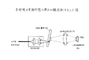
図17は、VIPA素子を用いた波長分散補償器の基本構成を示す図である。
VIPA素子は、ガラスなどの平行平板の両面に反射面を形成し、反射面の一部に光を入射するための照射窓を設けたものである。典型的な構成においては、反射面は、一方は反射率が約100%であり、他方が100%以下、典型的には95%などである。
【0004】
光通信に使用される光信号は、シングルモードファイバからラインフォーカサに入力される。ラインフォーカサでは、シングルモードファイバから広がって出てくる光を一旦平行光にし、その後、シリンドリカルレンズなどによって、線状に集光するものである。ラインフォーカサによって集光された光は、VIPA素子の照射窓を通って、VIPA素子の内部に集光する。
【0005】
VIPA素子にラインフォーカスされた光を入射すると、反対面から出射される光は、透過型グレーティングやプリズムのように角度分散を持った出射特性を持つ。すなわち、VIPA素子に入った光は、VIPA素子の反射面で反射され、VIPA素子内で多重反射を起こす。このとき、一方の反射面が反射率が100%より小さいことから、多重反射している光がすこしづつこの反射面から出力される。そして、出力された光が干渉を起こすことによって、波長によって進行方向の異なるビームを生成する。ここで、VIPA素子の出力側から見ると、反射する毎に出射される光は、それぞれ、異なった虚像VIから出力されているように見える。
【0006】
このビームをフォーカシングレンズで集光し、ミラーに反射させ、フォーカシングレンズ、VIPA素子を通り、ラインフォーカサを形成する、シングルモードファイバに結合する。すなわち、ミラーから反射され、フォーカシングレンズを通って、再びVIPA素子に光が入力される場合、1つの光線に着目したとき、この光線が出てきた虚像VIとVIPA素子に再び入射した、この光線が至る虚像VIとが光線の波長によって異なるようにすると、図17から分かるように、虚像VI間には、光学的距離の差分が生じているので、波長によって、光線が進む光学的距離が異なることになる。すなわち、光線の進む距離が波長によって異なるので、波長によって、光線がVIPA素子から出力される場合に、伝搬遅延が与えられて出力されることになる。よって、波長の異なる光線は異なる波長分散(色分散)を受けて、VIPA素子から出力されるようになる。この現象を利用して、波長分散補償器を構成しようとするのが、VIPA素子を利用した波長分散補償器である。
【0007】
【発明が解決しようとする課題】
しかし、この波長分散補償器への光の結合損失を最小にすると、VIPA素子有する挿入損失透過特性は平坦ではないため、波長多重光のような光信号に、このような波長分散補償器を使用した場合、波長によって、光信号のレベルが異なって出力されてしまうと言う問題がある。
【0008】
特に、近年実用化されつつある波長多重光通信システムにおいては、各波長の光は所定の光レベルを維持して伝送されることが望ましいので、光素子の透過チャネル帯域挿入損失波長特性の平坦化など最適化、ひいては、分散補償器周囲、システム及びネットワーク全体の透過チャネル帯域挿入損失平坦化などの最適化を行う必要がある。
【0009】
本発明の課題は、光の透過帯域を平坦化、あるいは、所望の特性とすることのできる分散補償器を提供することである。
【0010】
【課題を解決するための手段】
本発明の分散補償器は、入力光を波長毎に異なる方向に出射する角度分散手段と、該角度分散手段から出射された光を反射して、再び該角度分散手段に入射するミラー手段とからなる波長分散補償手段と、該波長分散補償手段の挿入損失波長特性を最適化する最適化手段とを備えることを特徴とする。
【0011】
本発明によれば、分散補償器の挿入損失波長特性を所望の特性に、特に、急峻な波長依存性を有する挿入損失波長特性を容易に平坦化することができる。また、分散補償器のみではなく、分散補償器を含む周辺装置や、これを含む光通信システム、光通信ネットワークなどの挿入損失波長特性も最適化手段によって所望の特性とすることができる。
【0012】
従って、分散補償器、これの周辺機器、光通信システム、光通信ネットワークなどの挿入損失波長特性が、光信号の伝搬する帯域に渡って急峻に変化していても、光信号の伝搬に適した特性に補正することができる。
【0013】
【発明の実施の形態】
本発明の実施形態においては、以下のような構成とその作用を提供する。
VIPA板(あるいはVIPA素子)とフォーカシングレンズ又はフォーカシングレンズとミラーとの間に透過率が2次元的に分布している空間フィルタを挿入する。あるいは、ミラー表面に、2次元の反射率を分布させる。更に、あるいは、ラインフォーカサにエタロンフィルタなどの透過損失特性が周期性を有している周期特性フィルタを挿入する。
【0014】
空間フィルタあるいは、周期特性フィルタを挿入することにより、分散補償器挿入損失特性と空間フィルタあるいは周期特性フィルタの透過損失特性が重畳され、最適化された、透過チャネル帯域挿入損失波長特性が得られる。
【0015】
また、ミラー反射率を2次元に分布させることにより、ミラー反射率特性と、本来の波長分散補償器挿入損失特性が重畳され、最適化された、透過チャネル帯域挿入損失波長特性が得られる。
【0016】
更に、周期的な透過特性が得られるエタロンフィルタを挿入することにより、分散補償器挿入損失特性とエタロンフィルタの透過損失特性が重畳された最適化された、透過チャネル帯域挿入損失波長特性が得られる。
【0017】
従って、波長分散補償器周囲、システム及びネットワーク全体の透過チャネル帯域挿入損失波長特性を平坦化等最適化が行える。
また、空間フィルタあるいは、ミラー反射率の制御は、以下のように行う。
【0018】
光吸収性のある元素、イオンまたは化合物が、光を吸収するので、その濃度を2次元に分布させることにより、透過率が2次元に分布した空間フィルタを得る。なお、光の透過率が小さくなる原理が光の吸収なので、反射光は問題とならない。
【0019】
金属反射膜は膜厚が薄いとき、膜厚によって反射率が変わるため、金属反射膜に2次元の膜厚分布を持たせることにより2次元の反射率分布を有するミラーを形成する。
【0020】
金属反射膜に2次元の膜厚分布を持たせると、ミラー表面の形状が設計された形状と異なってしまい、分散や群遅延などの光学特性が劣化することがある。そこで、ミラー基板の形状を金属膜の膜厚分布を見込んで形成し、所望のミラー形状を得るようにすることにより、光学特性の劣化を防ぐ。
【0021】
金属反射膜に2次元の膜厚分布を持たせると、ミラー表面の形状が設計された形状と異なってしまい、波長分散や群遅延などの光学特性が劣化することがある。
【0022】
そこで、2次元の膜厚分布を有する金属反射膜を2層(以上)とし、光の入射側第1層の金属反射膜に2次元の膜厚分布を持たせることにより反射率分布を生じさせると共に、金属反射膜全体の膜厚が一定となるように、光の入射側第2層の金属膜または誘電体膜が該第1層の金属膜とは逆の膜厚分布を持たせることにより、ミラー基板の表面形状を、設計値のまま保持することができ、光学特性の劣化を防ぐ。
【0023】
金属反射膜はスパッタや蒸着などの成膜手法により形成可能であるが、成膜粒子の進行を妨げるマスクを用いて、基板への成膜粒子の付着確率を変えることにより膜厚分布を形成する。
【0024】
図1は、本発明の実施形態の空間フィルタを用いた第1の構成例を示す図である。
図1に示されるように、本実施形態においては、図17で説明した角度分散補償器のVIPA素子10と、フォーカシングレンズ11の間、あるいは、フォーカシングレンズ11とミラー12の間に空間フィルタ13を設ける。
【0025】
ここで、ミラー12は一端が凹面で中央部が平面で他端が凸面に連続的に局面が変化するミラーである。
このミラー12を紙面方向(VIPAで角度分散を与えた方向)と直交する方向に曲面を連続的に変化させることで、波長分散量を任意の値に調整できる。
【0026】
このとき、空間フィルタ13はミラー12に対応させて移動する。
図2は、空間フィルタの透過損失分布とミラーの関係を示す図である。
図2においては、透過損失はL0からL5に行くに従って、大きくなっている。これは、VIPA素子あるいは、波長分散補償器全体の挿入損失特性が、透過帯域の中心付近で小さい損失であり、中心から離れるに従い急激に損失が大きくなる場合を想定している。この場合、透過帯域の中心付近に対応する空間フィルタの中心付近のL5領域で最も損失が大きく、空間フィルタの周辺に行くに従い、次第に損失の量が小さくなっている。
【0027】
ここで、空間フィルタ13は、ミラー12に対応させて移動するため、透過損失の分布は楕円形状に紙面左右方向に損失分布が集束するようにフィルタが構成されている。
【0028】
これは、ミラー12の移動した位置(矢印の方向に分散量に合わせて移動する)により角度分散を与えた光(VIPA素子からのビーム)に対して空間フィルタを通過する光の損失分布が異なるためである。
【0029】
すなわち、ミラー12の移動方向の端部は凸面及び凹面になっており、損失の分布がビームの角度分散する方向の外側に大きく分布しているため、空間フィルタ13はミラー12の曲面に対応して、ミラー12の移動方向に対して、楕円の損失分布を有している。
【0030】
損失の分布はミラーの曲面形状に対応して任意な損失の分布構成をとることができる。
図3は、本発明の実施形態の第2の構成例を示した図である。
【0031】
図3の構成例においては、ミラー12aの表面の反射率を2次元的に変化させ、強い光が照射する面では損失を大きく、弱い光が照射する面では損失を小さくする。
【0032】
図3においても、ミラー12aは、、図2と同様に紙面垂直方向に凹面から凸面に反射面が連続的に変化するミラーを移動させる。
図4は、2次元反射率分布ミラーの反射率分布を示している。
【0033】
図4においては、反射率は、R5からR0に行くに従い、次第に大きくなるように構成されている。図4の場合も、想定しているVIPA素子あるいは波長分散補償器の挿入損失特性は、図3の場合と同様である。従って、入射する光の強度が最も大きい透過帯域の中心付近であるR5領域で反射率が最も小さく、入射する光の強度が最も小さくなるR0領域で反射率は最大となっている。
【0034】
この反射率は図2の空間フィルタ13の透過損失の分布と同様に、反射面の曲面形状に対応して反射率の分布が構成される。
図5及び図6は、図1〜図4の実施形態の構成例の効果を説明する図である。
【0035】
図5は、空間フィルタを使った場合の最適化された挿入損失波長特性を示している。
波長分散補償器の挿入損失波長特性は、図5に示すように、波長分散補償器の挿入損失波長特性が、空間フィルタ透過損失波長特性と重畳することにより最適化され、最適化された挿入損失波長特性になる。ここで、最適化とは、波長分散補償器の挿入損失波長特性において、平坦化された透過チャネル帯域が拡大できることに限らず、空間フィルタの透過率を調整することにより、波長分散補償器周囲(波長分散補償器を含む周辺機器)、これを含む光通信システム及びこれを含む光通信ネットワーク全体の透過チャネル帯域のイコライジング及び挿入損失波長特性最適化を行うことである。
【0036】
図6は、ミラーの反射率を2次元的に変化させた場合の最適化された挿入損失波長特性を示す。
波長分散補償器の挿入損失波長特性は、図6に示すように、分散補償器の挿入損失波長特性が、2次元反射率分布ミラー反射率波長特性と重畳することにより最適化され、最適化された挿入損失波長特性になる。ここで、最適化とは、波長分散補償器の挿入損失波長特性において、平坦化された透過チャネル帯域が拡大できることに限らず、空間フィルタの透過率を調整することにより、波長分散補償器周囲(波長分散補償器を含む周辺機器)、これを含む光通信システム及びこれを含む光通信ネットワーク全体の透過チャネル帯域のイコライジング及び挿入損失特性最適化を行うことである。
【0037】
以上のように、適切な透過損失特性を有する空間フィルタ、あるいは、適切な反射率を有するミラーによって、波長分散補償器の挿入損失波長特性を平坦化できる。なお、上記したように、本実施形態によれば、空間フィルタの透過損失あるいはミラーの反射率を変化させることによって、さまざまに波長分散補償器の挿入損失波長特性を制御することができ、必ずしも透過帯域の平坦化のみに限定されるものではない。
【0038】
また、本実施形態の応用例としては、以下のようなものが考えられる。
(1)挿入損失−波長特性の波長周期特性を利用した光合分波器
米国特許5,809,190などの公知技術にあるような、図5に示す空間フィルタ透過損失波長特性が波長次元で周期的に繰り返す波長特性を有するデバイスを直列に接続し、図5に示す、最適化された挿入損失波長特性を実現することが可能である。
(2)波長透過率制御デバイス(エタロンなど)を用いた光信号波形劣化補償装置
特開平11−72756などの公知技術にあるような、エタロンなどによる、波長特性が波長次元で周期的に繰り返す波長特性を有するデバイスを直列に接続し、図5に示す、最適化された挿入損失波長特性を実現することが可能である。
【0039】
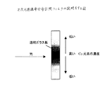
図7は、2次元透過率分布空間フィルタの説明をする図である。
図2のような2次元の透過率分布を有する空間フィルタは、図7に断面図を示すように、透明な材質、例えばガラスからなる板の中に、光吸収のある元素として、例えば、遷移金属であるCoを分散させ、その濃度を2次元に分布させることにより得ることができる。なお、ガラスの代わりにプラスチックなどの透明な材質を用いたり、Co以外の遷移金属元素であるCr、Cu、Fe、Ni、Mn、Vなどや、そのイオン、または酸化物や有機金属などの化合物、典型金属元素であるAl、希土類元素であるEr、Ndなどを用いても良い。
【0040】
こうして得られた2次元の透過率分布を有する空間フィルタを図1のように分散補償器のVIPA素子とミラーとの間に設置することにより、図5に示すような最適化された挿入損失波長特性を実現することが可能である。また、このとき、光ビームは空間フィルタを2回透過するので、その透過特性は2回の透過で図5の透過特性となるように設計しておく必要がある。なお、VIPA型分散補償器の原理上、図1のフォーカシングレンズ11とミラー12の間の位置で、なるべくミラー付近に該空間フィルタを設置した方が、波長によって空間フィルタを通過する位置が大きく異なるので、望ましい。
【0041】
なお、光の透過率が小さくなる原理が光の吸収なので、反射光が生じず、反射光が分散補償器の光学特性を劣化させることはない。また、本実施形態では、ガラスなどの透明基板に光吸収のある物質を2次元的に分布させた例を説明したが、このような光吸収のある物質の濃度を2次元的に分布させた吸収率分布膜や、光吸収のある膜の膜厚を2次元的に分布させた吸収分布膜としても良い。
【0042】
図8は、本発明の実施形態のエタロンフィルタを使用した別の構成例を示した図である。
図8に示すように、波長分散補償器のラインフォーカサ15のコリメートレンズ16とシリンドリカルレンズ17の間を往復するコリメートビーム中に周期的な透過特性を有するエタロンフィルタを挿入しても、図5に示すような最適化された挿入損失波長特性を実現することが可能である。このとき、ビームは、シングルモードファイバから入射して、ミラーで反射した後再びシングルモードファイバに入射する間に、エタロンフィルタを2回透過するので、その透過特性は2回の透過で図5の透過特性となるように設計しておく必要がある。
【0043】
ここで、例えば、図5のような分散補償器の挿入損失波長特性を平坦化する場合には、エタロンフィルタの透過率の低い部分を分散補償器の挿入損失波長特性の損失の小さいところに来るように調節する。
【0044】
この実施形態に於いては、先の実施形態のように、ミラー12の移動に対応してエタロンフィルタは移動せず固定である。
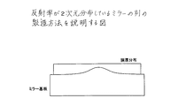
図9〜図13は、反射率が2次元的分布を示すミラーの製造方法について説明する図である。
【0045】
ミラーの金属反射膜に用いる金属としては、例えば、Auを用いることができるが、図9のようにAuの膜厚が80nm以下と薄い場合、膜厚と反射率に正の相関がある。よって、図10のように80nm以下の薄い範囲内でAuの膜厚分布を調整すれば、空間的に反射率が分布されたミラーとなる。図10の例では、ミラー基板の上に、中央の膜厚が薄いAuの金属反射膜が取り付けられている。この場合、図10の上段に示すように、Auの金属膜が80nm以内で膜厚の変化を示している場合には、ミラーの反射率に影響を与える。すなわち、A膜の薄い中央付近の反射ロスが大きく、従って、反射率が小さく設定できる。更に、図11のようにAuの膜厚分布を2次元的に分布させることにより、図4のように反射率を2次元に分布させることが可能である。
【0046】
図10のような膜厚分布は、例えば、図12のように、成膜粒子(Auの微粒子あるいは原子など)の進行を妨げるマスクを用いて、基板への成膜粒子の付着確率を変えることにより形成する事ができる。更に、図13のような2次元のマスクを用いることにより、図11のような2次元の膜厚分布を持たせることが可能である。
【0047】
なお、本実施形態ではAuを用いた場合を説明したが、Ag、Al、Crなど他の金属を用いても良く、特に限定されるものではない。
こうして得られた2次元の反射率を有するミラーを図3のように波長分散補償器に用いることにより、図6に示すような最適化された挿入損失波長特性を実現することが可能である。
【0048】
図14は、反射率が2次元分布しているミラーの別の製造方法を説明する図である。
図9〜図13のように金属膜を1層とした場合では、厳密に言えば、図10のように、ミラーの形状が実質的に金属膜の表面となるため、金属膜の膜厚分布により、本来のミラー基板の表面形状と異なってしまうおそれがある。VIPA素子を使った波長分散補償器では、ミラーの形状で波長分散補償器が光に与える波長分散や群遅延などの光学特性が決まるので、本来のミラー基板の形状と異なることにより、波長分散や、群遅延などの光学特性が劣化することがある。
【0049】
そこで、図14に示すように、予め膜厚分布を見込んでミラーの形状を作っておくことにより、所望のミラー形状を得ることができ、光学特性の劣化を防ぐことができる。
【0050】
図15及び図16は、反射率が2次元分布しているミラーの更に別の製造方法を説明する図である。
図14の製造方法でも膜厚分布による光学特性の劣化を防ぐことができるが、ミラーの加工が複雑となるという問題がある。
【0051】
そこで、図15に示すように、2次元の膜厚分布を有する金属反射膜を2層とし、光の入射側第1層の金属反射膜に2次元の膜厚分布を持たせることにより反射率分布を生じさせると共に、金属反射膜全体の膜厚が一定となるように、光の入射側第2層の膜に該第1層の金属膜とは逆の膜厚分布を持たせても良い。これにより、ミラー基板の表面形状を、設計値のまま保持するようにすることができ、光学特性の劣化を防ぐことができる。
【0052】
ここで、光の入射側第1層の金属反射膜として、反射率の高いAuを用いた場合、光の入射側第2層の膜としては反射率が低い(<4%)SiO2膜面からの反射は無視できるので、図9とほぼ同様のAu膜厚と反射率の相関が得られる。なお、SiO2以外にもAl2O3、MgF2、La2O3など他の誘電体膜も用いることができる。
【0053】
また、光の入射側第2層の膜として、反射率がやや高い(約68%)Crなどの十分に厚い金属膜を用いることもできる。その場合、Cr膜面から反射が無視できないが、図16のようにAu膜厚と反射率には正の相関があり、設計することは可能である。
【0054】
また、逆に、入射側第2層の膜として、反射率の高いAuを用い、光の入射側第1層として、反射率がやや低いCrなどの金属膜を用いて、1層目のCrに膜厚分布を持たせることにより、反射率分布を形成することも可能である。
【0055】
なお、金属反射膜の上にSiO2などの誘電体膜の保護膜や、金属反射膜の下にCrやNiなどのアンダーコートなどを付け足しても良く、層数が2層以上となってもかまわない。
【0056】
なお、上述した空間フィルタの透過損失、エタロンフィルタ、あるいは、ミラーの反射率の設計は、VIPA素子を使用した波長分散補償器の挿入損失特性と共に、コンピュータシミュレーションによって行うことができることは、当業者によれば容易に理解されるであろう。
【0057】
(付記1)入力光を波長毎に異なる方向に出射する角度分散手段と、該角度分散手段から出射された光を反射して、再び該角度分散手段に入射するミラー手段とからなる波長分散補償手段と、
該波長分散補償手段の挿入損失波長特性を最適化する最適化手段と、
を備えることを特徴とする分散補償器。
【0058】
(付記2)前記最適化手段は、2次元的に変化する透過損失特性を有する空間フィルタであることを特徴とする付記1に記載の分散補償器。
(付記3)前記最適化手段は、前記ミラー手段の反射面の反射率を2次元的に変化させることによって、該ミラー手段と一体化されていることを特徴とする付記1に記載の分散補償器。
【0059】
(付記4)前記最適化手段は、前記分散補償器が含まれる周辺機器、光通信システムあるいは、光通信ネットワークの透過チャネル帯域のイコライジングあるいは挿入損失波長特性の最適化も含めて最適化を行うことを特徴とする付記1に記載の分散補償器。
【0060】
(付記5)前記最適化手段は、エタロンフィルタであることを特徴とする付記1に記載の分散補償器。
(付記6)前記空間フィルタは、光吸収性のある元素、イオンまたは化合物の濃度が2次元的に変化するように添加されていることを特徴とする付記2に記載の分散補償器。
【0061】
(付記7)前記ミラーは、膜厚分布が2次元的に変化する反射膜からなることを特徴とする付記3に記載の分散補償器。
(付記8)前記ミラーは、前記反射膜と、該反射膜を搭載するミラー基板とからなり、該ミラー基板は、該反射膜の膜厚の変化による反射面の形状のゆがみを補償するように構成されていることを特徴とする付記7に記載の分散補償器。
【0062】
(付記9)前記反射膜は、少なくとも2層からなり、ある層が所望の反射率分布を提供するような膜厚を有し、他の層が該反射膜の全体の膜厚を一定にするように構成されていることを特徴とする付記7に記載の分散補償器。
【0063】
(付記10)前記他の層の膜厚分布は、前記ある層の膜厚分布の逆の分布をしていることを特徴とする付記9に記載の分散補償器。
(付記11)前記反射膜は、少なくとも2層からなり、ある層の反射率分布と、他の層の反射率分布を合成することによって所望の反射率分布を得るように構成されていることを特徴とする付記7に記載の分散補償器。
【0064】
(付記12)前記反射膜の2次元的に変化する膜厚分布は、基板への成膜粒子の付着確率を変化させることにより形成されることを特徴とする付記7に記載の分散補償器。
【0065】
【発明の効果】
波長分散補償器の挿入損失特性を最適化することによって、超高速、超大容量及び超長距離光波長多重伝送装置の特性改善が行える。
【図面の簡単な説明】
【図1】本発明の実施形態の空間フィルタを用いた第1の構成例を示す図である。
【図2】空間フィルタの透過損失分布のとミラーの関係を示した図である。
【図3】本発明の実施形態の第2の構成例を示した図である。
【図4】2次元反射率分布ミラーの反射率分布を示した図である。
【図5】空間フィルタを使った場合の最適化された挿入損失波長特性を示している。
【図6】ミラーの反射率を2次元的に変化させた場合の最適化された挿入損失波長特性を示す図である。
【図7】2次元透過率分布空間フィルタの説明をする図である。
【図8】本発明の実施形態のエタロンフィルタを使用した別の構成例を示した図である。
【図9】反射率が2次元的分布を示すミラーの製造方法について説明する図(その1)である。
【図10】反射率が2次元的分布を示すミラーの製造方法について説明する図(その2)である。
【図11】反射率が2次元的分布を示すミラーの製造方法について説明する図(その3)である。
【図12】反射率が2次元的分布を示すミラーの製造方法について説明する図(その4)である。
【図13】反射率が2次元的分布を示すミラーの製造方法について説明する図(その5)である。
【図14】反射率が2次元分布しているミラーの別の製造方法を説明する図である。
【図15】反射率が2次元分布しているミラーの更に別の製造方法を説明する図(その1)である。
【図16】反射率が2次元分布しているミラーの更に別の製造方法を説明する図(その2)である。
【図17】VIPA素子を用いた波長分散補償器の基本構成を示す図である。
【符号の説明】
10 VIPA素子
11 フォーカシングレンズ
12、12a ミラー
13 空間フィルタ
15 ラインフォーカサ
16 コリメートレンズ
17 シリンドリカルレンズ[0001]
BACKGROUND OF THE INVENTION
The present invention relates to a dispersion compensator for optical communication technology.
[0002]
[Prior art]
Recently, a chromatic dispersion compensator that compensates for chromatic dispersion in optical communication using an optical element called a VIPA element has been researched and developed.
[0003]
FIG. 17 is a diagram showing a basic configuration of a chromatic dispersion compensator using a VIPA element.
In the VIPA element, a reflecting surface is formed on both surfaces of a parallel plate such as glass, and an irradiation window for allowing light to enter is provided on a part of the reflecting surface. In a typical configuration, one of the reflective surfaces is about 100% reflective and the other is 100% or less, typically 95% or the like.
[0004]
An optical signal used for optical communication is input from a single mode fiber to a line focuser. In the line focuser, light that spreads out from a single mode fiber is once converted into parallel light, and then condensed into a linear shape by a cylindrical lens or the like. The light condensed by the line focuser passes through the irradiation window of the VIPA element and is condensed inside the VIPA element.
[0005]
When the line-focused light is incident on the VIPA element, the light emitted from the opposite surface has an emission characteristic with angular dispersion like a transmission type grating or a prism. That is, the light that enters the VIPA element is reflected by the reflection surface of the VIPA element, and causes multiple reflection in the VIPA element. At this time, since one of the reflective surfaces has a reflectance of less than 100%, the multiple reflected light is output from the reflective surface little by little. Then, the output light causes interference to generate beams having different traveling directions depending on the wavelength. Here, when viewed from the output side of the VIPA element, the light emitted each time it is reflected appears to be output from different virtual images VI.
[0006]
This beam is condensed by a focusing lens, reflected by a mirror, passed through the focusing lens and VIPA element, and coupled to a single mode fiber forming a line focuser. That is, when the light is reflected from the mirror, passes through the focusing lens, and is input again to the VIPA element, when attention is paid to one light beam, the virtual image VI from which the light beam has come out and the light beam again incident on the VIPA element. If the virtual image VI to be different from the virtual image VI depending on the wavelength of the light beam, as shown in FIG. 17, a difference in optical distance occurs between the virtual images VI. Therefore, the optical distance traveled by the light beam varies depending on the wavelength. It will be. That is, since the traveling distance of the light beam varies depending on the wavelength, when the light beam is output from the VIPA element depending on the wavelength, a propagation delay is given and the light beam is output. Therefore, light beams having different wavelengths receive different wavelength dispersion (chromatic dispersion) and are output from the VIPA element. It is a chromatic dispersion compensator using a VIPA element that attempts to construct a chromatic dispersion compensator using this phenomenon.
[0007]
[Problems to be solved by the invention]
However, if the coupling loss of light to this chromatic dispersion compensator is minimized, the insertion loss transmission characteristic of the VIPA element is not flat, so such a chromatic dispersion compensator is used for an optical signal such as wavelength multiplexed light. In this case, there is a problem that the level of the optical signal is output differently depending on the wavelength.
[0008]
In particular, in a wavelength division multiplexing optical communication system that has been put into practical use in recent years, it is desirable that each wavelength of light is transmitted while maintaining a predetermined optical level, so that the transmission channel band insertion loss wavelength characteristic of the optical element is flattened. In other words, it is necessary to perform optimization such as flattening the transmission channel band insertion loss around the dispersion compensator, the system, and the entire network.
[0009]
An object of the present invention is to provide a dispersion compensator capable of flattening a light transmission band or obtaining desired characteristics.
[0010]
[Means for Solving the Problems]
The dispersion compensator according to the present invention includes an angle dispersion unit that emits input light in different directions for each wavelength, and a mirror unit that reflects the light emitted from the angle dispersion unit and enters the angle dispersion unit again. Chromatic dispersion compensation means, and optimization means for optimizing the insertion loss wavelength characteristic of the chromatic dispersion compensation means.
[0011]
According to the present invention, it is possible to easily flatten an insertion loss wavelength characteristic of a dispersion compensator to a desired characteristic, in particular, an insertion loss wavelength characteristic having a steep wavelength dependency. Further, not only the dispersion compensator but also the insertion loss wavelength characteristic of a peripheral device including the dispersion compensator, an optical communication system including the dispersion compensator, an optical communication network, or the like can be set to a desired characteristic by the optimization unit.
[0012]
Therefore, even if the insertion loss wavelength characteristic of the dispersion compensator, its peripheral device, optical communication system, optical communication network, etc. changes sharply over the band in which the optical signal propagates, it is suitable for the propagation of the optical signal. The characteristic can be corrected.
[0013]
DETAILED DESCRIPTION OF THE INVENTION
In the embodiment of the present invention, the following configurations and operations are provided.
A spatial filter having a two-dimensional distribution of transmittance is inserted between the VIPA plate (or VIPA element) and the focusing lens or the focusing lens and the mirror. Alternatively, a two-dimensional reflectance is distributed on the mirror surface. Further, or alternatively, a periodic characteristic filter such as an etalon filter having periodic transmission loss characteristics is inserted into the line focuser.
[0014]
By inserting a spatial filter or a periodic characteristic filter, the dispersion compensator insertion loss characteristic and the transmission loss characteristic of the spatial filter or periodic characteristic filter are superimposed, and an optimized transmission channel band insertion loss wavelength characteristic is obtained.
[0015]
Also, by distributing the mirror reflectivity two-dimensionally, the mirror reflectivity characteristic and the original chromatic dispersion compensator insertion loss characteristic are superimposed, and an optimized transmission channel band insertion loss wavelength characteristic is obtained.
[0016]
Furthermore, by inserting an etalon filter that provides periodic transmission characteristics, an optimized transmission channel band insertion loss wavelength characteristic can be obtained in which the dispersion loss characteristics of the dispersion compensator and the transmission loss characteristic of the etalon filter are superimposed. .
[0017]
Therefore, it is possible to optimize the transmission channel band insertion loss wavelength characteristics around the chromatic dispersion compensator, the system, and the entire network.
The spatial filter or mirror reflectivity is controlled as follows.
[0018]
A light-absorbing element, ion, or compound absorbs light, and by distributing its concentration two-dimensionally, a spatial filter having two-dimensionally distributed transmittance is obtained. Since the principle of decreasing the light transmittance is light absorption, reflected light is not a problem.
[0019]
When the metal reflective film is thin, the reflectivity changes depending on the film thickness. Therefore, a mirror having a two-dimensional reflectivity distribution is formed by giving the metal reflective film a two-dimensional film thickness distribution.
[0020]
If the metal reflection film has a two-dimensional film thickness distribution, the shape of the mirror surface is different from the designed shape, and optical characteristics such as dispersion and group delay may be deteriorated. Therefore, the mirror substrate is formed in consideration of the film thickness distribution of the metal film to obtain a desired mirror shape, thereby preventing the deterioration of the optical characteristics.
[0021]
If the metal reflective film has a two-dimensional film thickness distribution, the shape of the mirror surface is different from the designed shape, and optical characteristics such as wavelength dispersion and group delay may be deteriorated.
[0022]
Therefore, the metal reflection film having a two-dimensional film thickness distribution is made into two layers (or more), and the light reflection side first layer metal reflection film has a two-dimensional film thickness distribution to generate a reflectance distribution. At the same time, the metal film or dielectric film on the light incident side second layer has a film thickness distribution opposite to that of the first layer metal film so that the film thickness of the entire metal reflection film is constant. The surface shape of the mirror substrate can be kept at the design value, and deterioration of the optical characteristics is prevented.
[0023]
The metal reflective film can be formed by a film formation technique such as sputtering or vapor deposition, but the film thickness distribution is formed by changing the adhesion probability of the film formation particles to the substrate using a mask that prevents the progress of the film formation particles. .
[0024]
FIG. 1 is a diagram illustrating a first configuration example using a spatial filter according to an embodiment of the present invention.
As shown in FIG. 1, in this embodiment, a
[0025]
Here, the mirror 12 is a mirror whose one end is a concave surface, the central portion is a flat surface, and the other end is a convex surface, and the aspect changes continuously.
The amount of chromatic dispersion can be adjusted to an arbitrary value by continuously changing the curved surface of the mirror 12 in a direction orthogonal to the paper surface direction (direction in which angular dispersion is given by VIPA).
[0026]
At this time, the
FIG. 2 is a diagram showing the relationship between the transmission loss distribution of the spatial filter and the mirror.
In FIG. 2, the transmission loss increases as it goes from L0 to L5. This assumes that the insertion loss characteristic of the VIPA element or the entire chromatic dispersion compensator is a small loss near the center of the transmission band, and the loss increases rapidly as the distance from the center increases. In this case, the loss is greatest in the L5 region near the center of the spatial filter corresponding to the vicinity of the center of the transmission band, and the amount of loss gradually decreases toward the periphery of the spatial filter.
[0027]
Here, since the
[0028]
This is because the loss distribution of light passing through the spatial filter differs from the light (beam from the VIPA element) given angular dispersion depending on the position of the mirror 12 (moving in the direction of the arrow according to the amount of dispersion). Because.
[0029]
That is, the end in the moving direction of the mirror 12 is convex and concave, and the loss distribution is greatly distributed outside the beam angle dispersion direction, so the
[0030]
The loss distribution can take any loss distribution configuration corresponding to the curved surface shape of the mirror.
FIG. 3 is a diagram illustrating a second configuration example of the embodiment of the present invention.
[0031]
In the configuration example of FIG. 3, the reflectance of the surface of the mirror 12a is two-dimensionally changed to increase the loss on the surface irradiated with strong light and reduce the loss on the surface irradiated with weak light.
[0032]
Also in FIG. 3, the mirror 12a moves the mirror whose reflection surface continuously changes from the concave surface to the convex surface in the direction perpendicular to the paper surface as in FIG.
FIG. 4 shows the reflectance distribution of the two-dimensional reflectance distribution mirror.
[0033]
In FIG. 4, the reflectance is configured to gradually increase from R5 to R0. Also in the case of FIG. 4, the insertion loss characteristic of the assumed VIPA element or chromatic dispersion compensator is the same as that of FIG. Therefore, the reflectance is the smallest in the R5 region near the center of the transmission band where the intensity of the incident light is the highest, and the reflectance is the largest in the R0 region where the intensity of the incident light is the smallest.
[0034]
Similar to the distribution of transmission loss of the
5 and 6 are diagrams for explaining the effects of the configuration example of the embodiment of FIGS.
[0035]
FIG. 5 shows an optimized insertion loss wavelength characteristic when a spatial filter is used.
As shown in FIG. 5, the insertion loss wavelength characteristic of the chromatic dispersion compensator is optimized by superimposing the insertion loss wavelength characteristic of the chromatic dispersion compensator on the spatial filter transmission loss wavelength characteristic. It becomes wavelength characteristic. Here, the optimization is not limited to the expansion of the flattened transmission channel band in the insertion loss wavelength characteristic of the chromatic dispersion compensator, but by adjusting the transmittance of the spatial filter, Peripheral devices including a chromatic dispersion compensator), optical communication system including the same, and equalization of the transmission channel band of the entire optical communication network including the same and optimization of insertion loss wavelength characteristics.
[0036]
FIG. 6 shows the optimized insertion loss wavelength characteristic when the reflectance of the mirror is changed two-dimensionally.
As shown in FIG. 6, the insertion loss wavelength characteristic of the chromatic dispersion compensator is optimized and optimized by superimposing the insertion loss wavelength characteristic of the dispersion compensator on the two-dimensional reflectance distribution mirror reflectance wavelength characteristic. Insertion loss wavelength characteristics. Here, the optimization is not limited to the expansion of the flattened transmission channel band in the insertion loss wavelength characteristic of the chromatic dispersion compensator, but by adjusting the transmittance of the spatial filter, Peripheral devices including a chromatic dispersion compensator), an optical communication system including the same, and an equalization of a transmission channel band and an insertion loss characteristic optimization of the entire optical communication network including the same.
[0037]
As described above, the insertion loss wavelength characteristic of the chromatic dispersion compensator can be flattened by a spatial filter having an appropriate transmission loss characteristic or a mirror having an appropriate reflectance. As described above, according to the present embodiment, the insertion loss wavelength characteristic of the chromatic dispersion compensator can be controlled variously by changing the transmission loss of the spatial filter or the reflectance of the mirror, and the transmission loss is not necessarily transmitted. It is not limited to band flattening.
[0038]
Moreover, the following can be considered as an application example of this embodiment.
(1) Optical multiplexer / demultiplexer using wavelength period characteristics of insertion loss-wavelength characteristics
As shown in FIG. 5, devices having wavelength characteristics in which the spatial filter transmission loss wavelength characteristics shown in FIG. 5 repeat periodically in the wavelength dimension, as in known techniques such as US Pat. No. 5,809,190, are shown in FIG. An optimized insertion loss wavelength characteristic can be realized.
(2) Optical signal waveform deterioration compensation device using wavelength transmittance control device (etalon, etc.)
Optimized insertion loss shown in FIG. 5 is obtained by connecting in series a device having a wavelength characteristic that repeats periodically in the wavelength dimension, such as an etalon, as in a known technique such as JP-A-11-72756. It is possible to realize wavelength characteristics.
[0039]
FIG. 7 is a diagram illustrating a two-dimensional transmittance distribution spatial filter.
A spatial filter having a two-dimensional transmittance distribution as shown in FIG. 2 has, for example, a transition as a light-absorbing element in a transparent material, for example, a glass plate, as shown in FIG. It can be obtained by dispersing Co, which is a metal, and distributing its concentration two-dimensionally. In addition, transparent materials such as plastic are used instead of glass, transition metal elements other than Co, such as Cr, Cu, Fe, Ni, Mn, and V, ions thereof, or compounds such as oxides and organic metals Al, which is a typical metal element, Er, Nd, which is a rare earth element, or the like may be used.
[0040]
By installing the spatial filter having the two-dimensional transmittance distribution thus obtained between the VIPA element and the mirror of the dispersion compensator as shown in FIG. 1, the optimized insertion loss wavelength as shown in FIG. It is possible to realize the characteristics. At this time, since the light beam passes through the spatial filter twice, it is necessary to design the transmission characteristic so that the transmission characteristic shown in FIG. Note that, based on the principle of the VIPA type dispersion compensator, the position where the spatial filter is installed in the vicinity of the mirror as much as possible between the focusing lens 11 and the mirror 12 in FIG. So desirable.
[0041]
Since the principle of decreasing the light transmittance is light absorption, no reflected light is generated, and the reflected light does not deteriorate the optical characteristics of the dispersion compensator. In this embodiment, an example in which a light-absorbing substance is distributed two-dimensionally on a transparent substrate such as glass has been described. However, the concentration of such a light-absorbing substance is two-dimensionally distributed. An absorption distribution film or an absorption distribution film in which the film thickness of a light absorbing film is two-dimensionally distributed may be used.
[0042]
FIG. 8 is a diagram showing another configuration example using the etalon filter of the embodiment of the present invention.
As shown in FIG. 8, even if an etalon filter having periodic transmission characteristics is inserted into the collimated beam reciprocating between the collimating lens 16 and the cylindrical lens 17 of the line focuser 15 of the chromatic dispersion compensator, FIG. It is possible to realize an optimized insertion loss wavelength characteristic as shown in FIG. At this time, since the beam is incident from the single mode fiber, reflected by the mirror, and then incident on the single mode fiber again, it passes through the etalon filter twice. It is necessary to design so as to have transmission characteristics.
[0043]
Here, for example, when flattening the insertion loss wavelength characteristic of the dispersion compensator as shown in FIG. Adjust as follows.
[0044]
In this embodiment, as in the previous embodiment, the etalon filter does not move in response to the movement of the mirror 12 and is fixed.
9 to 13 are diagrams for explaining a method for manufacturing a mirror having a two-dimensional distribution of reflectance.
[0045]
As the metal used for the metal reflective film of the mirror, for example, Au can be used. However, when the film thickness of Au is as thin as 80 nm or less as shown in FIG. 9, there is a positive correlation between the film thickness and the reflectance. Therefore, if the film thickness distribution of Au is adjusted within a thin range of 80 nm or less as shown in FIG. 10, a mirror with spatially distributed reflectance is obtained. In the example of FIG. 10, an Au metal reflection film with a thin central film thickness is attached on a mirror substrate. In this case, as shown in the upper part of FIG. 10, when the Au metal film shows a change in film thickness within 80 nm, the reflectivity of the mirror is affected. That is, the reflection loss near the thin center of the A film is large, and therefore the reflectance can be set small. Further, by distributing the Au film thickness distribution two-dimensionally as shown in FIG. 11, the reflectance can be distributed two-dimensionally as shown in FIG.
[0046]
The film thickness distribution as shown in FIG. 10 changes the adhesion probability of the film formation particles to the substrate by using a mask that prevents the progress of the film formation particles (Au fine particles or atoms, for example) as shown in FIG. Can be formed. Furthermore, by using a two-dimensional mask as shown in FIG. 13, it is possible to have a two-dimensional film thickness distribution as shown in FIG.
[0047]
In the present embodiment, the case of using Au has been described, but other metals such as Ag, Al, and Cr may be used and are not particularly limited.
By using the thus obtained mirror having a two-dimensional reflectivity in the chromatic dispersion compensator as shown in FIG. 3, it is possible to realize the optimized insertion loss wavelength characteristic as shown in FIG.
[0048]
FIG. 14 is a diagram for explaining another method for manufacturing a mirror in which the reflectance is two-dimensionally distributed.
Strictly speaking, in the case where one metal film is formed as shown in FIGS. 9 to 13, since the shape of the mirror is substantially the surface of the metal film as shown in FIG. 10, the film thickness distribution of the metal film. As a result, the surface shape of the original mirror substrate may be different. In a chromatic dispersion compensator using a VIPA element, optical characteristics such as chromatic dispersion and group delay given to light by the chromatic dispersion compensator are determined by the shape of the mirror. Optical characteristics such as group delay may be deteriorated.
[0049]
Therefore, as shown in FIG. 14, by preparing the shape of the mirror in consideration of the film thickness distribution in advance, a desired mirror shape can be obtained, and deterioration of optical characteristics can be prevented.
[0050]
15 and 16 are diagrams for explaining another method for manufacturing a mirror having a two-dimensional reflectance distribution.
Although the manufacturing method of FIG. 14 can prevent the deterioration of the optical characteristics due to the film thickness distribution, there is a problem that the processing of the mirror becomes complicated.
[0051]
Therefore, as shown in FIG. 15, the metal reflection film having a two-dimensional film thickness distribution is made into two layers, and the metal reflection film on the light incident side first layer has a two-dimensional film thickness distribution so that the reflectivity is obtained. The film on the light incident side second layer may have a film thickness distribution opposite to that of the metal film on the first layer so as to cause the distribution and the film thickness of the entire metal reflection film to be constant. . As a result, the surface shape of the mirror substrate can be maintained as the design value, and deterioration of the optical characteristics can be prevented.
[0052]
Here, when Au having high reflectivity is used as the metal reflective film on the first layer on the light incident side, the reflectivity is low (<4%) as the film on the second layer on the light incident side. 2 Since the reflection from the film surface is negligible, the correlation between the Au film thickness and the reflectance is almost the same as in FIG. In addition, SiO 2 Besides Al 2 O Three , MgF 2 , La 2 O Three Other dielectric films can also be used.
[0053]
Also, a sufficiently thick metal film such as Cr having a slightly high reflectance (about 68%) can be used as the film on the light incident side second layer. In that case, reflection from the Cr film surface cannot be ignored, but the Au film thickness and reflectance have a positive correlation as shown in FIG. 16, and can be designed.
[0054]
On the other hand, as the incident-side second layer film, Au having a high reflectance is used, and as the incident-side first layer, a metal film such as Cr having a slightly low reflectance is used, the first layer Cr It is also possible to form a reflectance distribution by providing a film thickness distribution.
[0055]
In addition, SiO on the metal reflective film 2 A protective film such as a dielectric film, or an undercoat such as Cr or Ni may be added under the metal reflective film, and the number of layers may be two or more.
[0056]
It is to be understood by those skilled in the art that the transmission loss of the spatial filter, the etalon filter, or the mirror reflectivity can be designed by computer simulation together with the insertion loss characteristic of the chromatic dispersion compensator using the VIPA element. Will be easily understood.
[0057]
(Supplementary note 1) Chromatic dispersion compensation comprising angle dispersion means for emitting input light in different directions for each wavelength, and mirror means for reflecting light emitted from the angle dispersion means and entering the angle dispersion means again Means,
Optimization means for optimizing the insertion loss wavelength characteristic of the chromatic dispersion compensation means;
A dispersion compensator comprising:
[0058]
(Supplementary note 2) The dispersion compensator according to supplementary note 1, wherein the optimization means is a spatial filter having a transmission loss characteristic that changes two-dimensionally.
(Supplementary note 3) The dispersion compensation according to supplementary note 1, wherein the optimization means is integrated with the mirror means by two-dimensionally changing the reflectance of the reflection surface of the mirror means. vessel.
[0059]
(Additional remark 4) The said optimization means optimizes also including the equalization of the permeation | transmission channel band of the peripheral device in which the said dispersion compensator is included, an optical communication system, or an optical communication network, or the optimization of an insertion loss wavelength characteristic The dispersion compensator according to appendix 1, characterized by:
[0060]
(Supplementary note 5) The dispersion compensator according to supplementary note 1, wherein the optimization means is an etalon filter.
(Supplementary note 6) The dispersion compensator according to
[0061]
(Supplementary note 7) The dispersion compensator according to
(Supplementary Note 8) The mirror includes the reflective film and a mirror substrate on which the reflective film is mounted, and the mirror substrate compensates for the distortion of the shape of the reflective surface due to the change in the thickness of the reflective film. The dispersion compensator according to appendix 7, which is configured.
[0062]
(Additional remark 9) The said reflecting film consists of at least two layers, and has a film thickness that a certain layer provides desired reflectance distribution, and another layer makes the whole film thickness of this reflecting film constant. The dispersion compensator according to appendix 7, which is configured as described above.
[0063]
(Supplementary note 10) The dispersion compensator according to
(Supplementary Note 11) The reflective film is composed of at least two layers, and is configured to obtain a desired reflectance distribution by combining the reflectance distribution of one layer and the reflectance distribution of another layer. The dispersion compensator according to appendix 7, which is characterized.
[0064]
(Supplementary note 12) The dispersion compensator according to supplementary note 7, wherein the two-dimensionally changing film thickness distribution of the reflective film is formed by changing a probability of adhesion of film formation particles to the substrate.
[0065]
【The invention's effect】
By optimizing the insertion loss characteristics of the chromatic dispersion compensator, it is possible to improve the characteristics of the ultra-high speed, ultra-large capacity and ultra-long-distance optical wavelength division multiplexing transmission apparatus.
[Brief description of the drawings]
FIG. 1 is a diagram illustrating a first configuration example using a spatial filter according to an embodiment of the present invention.
FIG. 2 is a diagram showing a relationship between a transmission loss distribution of a spatial filter and a mirror.
FIG. 3 is a diagram showing a second configuration example of an embodiment of the present invention.
FIG. 4 is a diagram showing a reflectance distribution of a two-dimensional reflectance distribution mirror.
FIG. 5 shows an optimized insertion loss wavelength characteristic when a spatial filter is used.
FIG. 6 is a diagram showing optimized insertion loss wavelength characteristics when the reflectance of the mirror is changed two-dimensionally.
FIG. 7 is a diagram illustrating a two-dimensional transmittance distribution spatial filter.
FIG. 8 is a diagram showing another configuration example using the etalon filter according to the embodiment of the present invention.
FIG. 9 is a diagram (part 1) illustrating a method for manufacturing a mirror having a two-dimensional distribution of reflectance.
FIG. 10 is a diagram (No. 2) for explaining a method for manufacturing a mirror having a two-dimensional distribution of reflectance.
FIG. 11 is a diagram (No. 3) for explaining the manufacturing method of the mirror having a two-dimensional reflectance distribution;
FIG. 12 is a diagram (No. 4) for explaining the manufacturing method of the mirror having a two-dimensional distribution of reflectance.
FIG. 13 is a diagram (No. 5) for explaining the manufacturing method of the mirror having a two-dimensional distribution of reflectance.
FIG. 14 is a diagram for explaining another method for manufacturing a mirror in which the reflectance is two-dimensionally distributed.
FIG. 15 is a diagram (No. 1) for explaining still another method of manufacturing a mirror having a two-dimensional distribution of reflectance.
FIG. 16 is a diagram (No. 2) for explaining still another method of manufacturing a mirror having a two-dimensional distribution of reflectance.
FIG. 17 is a diagram showing a basic configuration of a chromatic dispersion compensator using a VIPA element.
[Explanation of symbols]
10 VIPA elements
11 Focusing lens
12, 12a Mirror
13 Spatial filter
15 Line Focus
16 Collimating lens
17 Cylindrical lens
Claims (5)
該角度分散手段から出射された光を反射して、再び該角度分散手段に入射するミラー手段とを有する波長分散補償手段と、
前記角度分散手段と前記ミラー手段との間に配置され、前記角度分散手段により角度分散された光が入射する面内において2次元的に変化する反射損失特性または透過損失特性を有し、該波長分散補償手段の挿入損失波長特性を最適化する最適化手段と、
を備えることを特徴とする分散補償器。Angular dispersion means using a VIPA element that emits input light in different directions for each wavelength;
Chromatic dispersion compensating means having mirror means for reflecting the light emitted from the angular dispersion means and entering the angular dispersion means again;
A reflection loss characteristic or a transmission loss characteristic that is arranged between the angle dispersion means and the mirror means and changes two-dimensionally in a plane on which the light angle-dispersed by the angle dispersion means is incident; An optimization means for optimizing the insertion loss wavelength characteristic of the dispersion compensation means;
A dispersion compensator comprising:
Priority Applications (4)
| Application Number | Priority Date | Filing Date | Title |
|---|---|---|---|
| JP2002006824A JP4030763B2 (en) | 2002-01-16 | 2002-01-16 | Transmission band flattened dispersion compensator |
| US10/340,842 US6909537B2 (en) | 2002-01-16 | 2003-01-13 | Dispersion compensator whose transmission band is flattened |
| EP03000628A EP1333309B1 (en) | 2002-01-16 | 2003-01-15 | Dispersion compensator with flattened transmission band |
| DE60304750T DE60304750T2 (en) | 2002-01-16 | 2003-01-15 | Dispersion compensator with a flat transmission curve |
Applications Claiming Priority (1)
| Application Number | Priority Date | Filing Date | Title |
|---|---|---|---|
| JP2002006824A JP4030763B2 (en) | 2002-01-16 | 2002-01-16 | Transmission band flattened dispersion compensator |
Publications (2)
| Publication Number | Publication Date |
|---|---|
| JP2003207618A JP2003207618A (en) | 2003-07-25 |
| JP4030763B2 true JP4030763B2 (en) | 2008-01-09 |
Family
ID=19191275
Family Applications (1)
| Application Number | Title | Priority Date | Filing Date |
|---|---|---|---|
| JP2002006824A Expired - Fee Related JP4030763B2 (en) | 2002-01-16 | 2002-01-16 | Transmission band flattened dispersion compensator |
Country Status (4)
| Country | Link |
|---|---|
| US (1) | US6909537B2 (en) |
| EP (1) | EP1333309B1 (en) |
| JP (1) | JP4030763B2 (en) |
| DE (1) | DE60304750T2 (en) |
Families Citing this family (5)
| Publication number | Priority date | Publication date | Assignee | Title |
|---|---|---|---|---|
| US6714705B1 (en) * | 2002-05-07 | 2004-03-30 | Avanex Corporation | Tunable chromatic dispersion and dispersion slope compensator utilizing a virtually imaged phased array and a rotating grating |
| JP4518825B2 (en) * | 2004-03-31 | 2010-08-04 | 富士通株式会社 | Variable wavelength dispersion compensator |
| JP2006243500A (en) | 2005-03-04 | 2006-09-14 | Fujitsu Ltd | Wavelength dispersion compensator |
| JP4613814B2 (en) * | 2005-12-26 | 2011-01-19 | 日立金属株式会社 | Variable dispersion compensator |
| JP7203812B2 (en) * | 2018-02-14 | 2023-01-13 | 古河電気工業株式会社 | Optical module, its wavelength control method and its calibration method |
Family Cites Families (13)
| Publication number | Priority date | Publication date | Assignee | Title |
|---|---|---|---|---|
| CA2146384C (en) | 1995-04-05 | 1999-05-11 | Joseph Ip | Chromatic dispersion compensation device |
| JP3464081B2 (en) * | 1995-07-26 | 2003-11-05 | 富士通株式会社 | Wavelength splitter |
| US5930045A (en) * | 1995-07-26 | 1999-07-27 | Fujitsu, Ltd. | Optical apparatus which uses a virtually imaged phased array to produce chromatic dispersion |
| US5969865A (en) * | 1995-07-26 | 1999-10-19 | Fujitsu Limited | Optical apparatus which uses a virtually imaged phased array to produce chromatic dispersion |
| US6028706A (en) | 1995-07-26 | 2000-02-22 | Fujitsu Limited | Virtually imaged phased array (VIPA) having a varying reflectivity surface to improve beam profile |
| US5973838A (en) * | 1995-07-26 | 1999-10-26 | Fujitsu Limited | Apparatus which includes a virtually imaged phased array (VIPA) in combination with a wavelength splitter to demultiplex wavelength division multiplexed (WDM) light |
| US6332689B1 (en) | 1999-12-14 | 2001-12-25 | Fujitsu Limited | Optical apparatus which uses a virtually imaged phased array to produce chromatic dispersion |
| US6556320B1 (en) * | 2000-05-19 | 2003-04-29 | Avanex Corporation | Tunable chromatic dispersion, dispersion slope, and polarization mode dispersion compensator utilizing a virtually imaged phased array |
| US6744991B1 (en) * | 2000-05-19 | 2004-06-01 | Avanex Corporation | Tunable chromatic dispersion and polarization mode dispersion compensator utilizing a virtually imaged phased array |
| JP2002311235A (en) | 2000-09-14 | 2002-10-23 | Oyokoden Lab Co Ltd | Composite light diffusion compensating element and light diffusion compensating method using the same |
| US6668115B2 (en) * | 2000-12-22 | 2003-12-23 | Avanex Corporation | Method, apparatus, and system for compensation of amplifier gain slope and chromatic dispersion utilizing a virtually imaged phased array |
| JP3994737B2 (en) | 2002-01-09 | 2007-10-24 | 富士通株式会社 | Optical device |
| US6714705B1 (en) * | 2002-05-07 | 2004-03-30 | Avanex Corporation | Tunable chromatic dispersion and dispersion slope compensator utilizing a virtually imaged phased array and a rotating grating |
-
2002
- 2002-01-16 JP JP2002006824A patent/JP4030763B2/en not_active Expired - Fee Related
-
2003
- 2003-01-13 US US10/340,842 patent/US6909537B2/en not_active Expired - Fee Related
- 2003-01-15 DE DE60304750T patent/DE60304750T2/en not_active Expired - Fee Related
- 2003-01-15 EP EP03000628A patent/EP1333309B1/en not_active Expired - Fee Related
Also Published As
| Publication number | Publication date |
|---|---|
| US20030147121A1 (en) | 2003-08-07 |
| JP2003207618A (en) | 2003-07-25 |
| DE60304750D1 (en) | 2006-06-01 |
| DE60304750T2 (en) | 2007-05-16 |
| EP1333309B1 (en) | 2006-04-26 |
| EP1333309A3 (en) | 2004-12-08 |
| EP1333309A2 (en) | 2003-08-06 |
| US6909537B2 (en) | 2005-06-21 |
Similar Documents
| Publication | Publication Date | Title |
|---|---|---|
| US6471361B2 (en) | Optical apparatus which uses a virtually imaged phased array to produce chromatic dispersion | |
| US7193778B2 (en) | Optical apparatus which uses a virtually imaged phased array to produce chromatic dispersion | |
| US7075723B2 (en) | Optical apparatus which uses a virtually imaged phased array to produce chromatic dispersion | |
| JP2002514323A (en) | Optical device using VIPA (virtual imaged phased array) for chromatic dispersion | |
| TW594082B (en) | Compensating for chromatic dispersion in optical fibers | |
| JP2002267998A (en) | Wavelength dispersion compensation module, optical receiving circuit, and optical communication system | |
| JP4030763B2 (en) | Transmission band flattened dispersion compensator | |
| US6956700B1 (en) | Wavelength dispersion compensating apparatus | |
| US7646982B2 (en) | Chromatic dispersion compensator | |
| JP4052114B2 (en) | Variable optical dispersion compensator | |
| JP2004085915A (en) | Wavelength dispersion generator, and polygon mirror used in the wavelength dispersion generator and its manufacturing method | |
| JP2006221075A (en) | Variable dispersion compensator | |
| JP2000111831A (en) | Virtually imaged phased array(vipa) equipped with spacer member and optical-path length adjusting member | |
| JP2003315697A (en) | Dispersion compensator |
Legal Events
| Date | Code | Title | Description |
|---|---|---|---|
| A621 | Written request for application examination |
Free format text: JAPANESE INTERMEDIATE CODE: A621 Effective date: 20041224 |
|
| A977 | Report on retrieval |
Free format text: JAPANESE INTERMEDIATE CODE: A971007 Effective date: 20070122 |
|
| A131 | Notification of reasons for refusal |
Free format text: JAPANESE INTERMEDIATE CODE: A131 Effective date: 20070206 |
|
| A521 | Request for written amendment filed |
Free format text: JAPANESE INTERMEDIATE CODE: A523 Effective date: 20070409 |
|
| TRDD | Decision of grant or rejection written | ||
| A01 | Written decision to grant a patent or to grant a registration (utility model) |
Free format text: JAPANESE INTERMEDIATE CODE: A01 Effective date: 20071016 |
|
| A61 | First payment of annual fees (during grant procedure) |
Free format text: JAPANESE INTERMEDIATE CODE: A61 Effective date: 20071017 |
|
| R150 | Certificate of patent or registration of utility model |
Free format text: JAPANESE INTERMEDIATE CODE: R150 |
|
| FPAY | Renewal fee payment (event date is renewal date of database) |
Free format text: PAYMENT UNTIL: 20101026 Year of fee payment: 3 |
|
| LAPS | Cancellation because of no payment of annual fees |