JP4022073B2 - Non-contact / contact IC card communication control device and mobile phone device - Google Patents
Non-contact / contact IC card communication control device and mobile phone device Download PDFInfo
- Publication number
- JP4022073B2 JP4022073B2 JP2002022621A JP2002022621A JP4022073B2 JP 4022073 B2 JP4022073 B2 JP 4022073B2 JP 2002022621 A JP2002022621 A JP 2002022621A JP 2002022621 A JP2002022621 A JP 2002022621A JP 4022073 B2 JP4022073 B2 JP 4022073B2
- Authority
- JP
- Japan
- Prior art keywords
- contact
- communication
- card
- contact communication
- cutoff
- Prior art date
- Legal status (The legal status is an assumption and is not a legal conclusion. Google has not performed a legal analysis and makes no representation as to the accuracy of the status listed.)
- Expired - Fee Related
Links
- 238000004891 communication Methods 0.000 title claims description 200
- 238000001514 detection method Methods 0.000 claims description 19
- 230000000694 effects Effects 0.000 claims description 5
- 230000007613 environmental effect Effects 0.000 claims 1
- 230000006870 function Effects 0.000 description 12
- 238000010586 diagram Methods 0.000 description 10
- 238000000034 method Methods 0.000 description 10
- 239000003990 capacitor Substances 0.000 description 8
- 230000000903 blocking effect Effects 0.000 description 3
- 230000005540 biological transmission Effects 0.000 description 2
- 230000001413 cellular effect Effects 0.000 description 1
- 239000004020 conductor Substances 0.000 description 1
- 230000008878 coupling Effects 0.000 description 1
- 238000010168 coupling process Methods 0.000 description 1
- 238000005859 coupling reaction Methods 0.000 description 1
- 230000005674 electromagnetic induction Effects 0.000 description 1
- 230000010365 information processing Effects 0.000 description 1
- 238000012986 modification Methods 0.000 description 1
- 230000004048 modification Effects 0.000 description 1
- 230000035945 sensitivity Effects 0.000 description 1
Images


Description
【0001】
【発明の属する技術分野】
本発明は、非接触式及び接触式の両方の通信手段を持つICチップを搭載する非接触/接触両用ICカードの通信を制御する、携帯可能な非接触/接触両用ICカード通信制御装置及びこの非接触/接触両用ICカード通信制御装置を備え、無線接続された基地局を介して無線通信を行う携帯電話装置に関するものである。
【0002】
【従来の技術】
従来から、携帯電話、携帯情報端末(PDA)等の携帯端末は、非接触/接触両用ICカードの認証(身分証明を含む)、決済等の諸機能を利用するため、非接触/接触両用ICカードを格納し、接触式で通信を行っている。非接触/接触両用ICカードとは、電磁波を介して電力供給を受け、同様にデータを電送する非接触式と、伝導体によって形成される端子を介して電力の供給を受け、同様にデータを電送する接触式の両方の通信方式を兼ね備えたICカードであって、携帯端末に装填され、接触式の通信によってその機能を利用されるSIMカード等のカードを含む。
【0003】
図5は、従来の非接触/接触両用ICカードを示すブロック図である。
非接触/接触両用ICカード2は、カード基材内にICチップ21、アンテナコイル22等、カード基材表面の所定の位置に接触端子23等が設けられている。アンテナコイル22及び接触端子23は、ICチップ21に接続されている。ICチップ21は、整流回路211、定電圧回路212、動作方式検知部213、復/変調回路214、揮発性メモリ215、ROM216、不揮発性メモリ217、CPU218等を備えている。CPU218が揮発性メモリ215等の作業領域を利用してROM216、不揮発性メモリ217等の記憶部に記憶されているプログラムを実行することによって、非接触式及び接触式の通信手段として機能する等、各部を制御する。
【0004】
ICチップ21は、非接触通信手段によって、アンテナコイル22を通じて図示しない外部装置であるリーダライタから送出される搬送波である交流電磁波を受信し、電磁誘導によって電力、クロックの供給を受け、情報送受信を行う。
また、ICチップ21は、接触式の通信手段によって、接触端子23がリーダライタの接触端子と接触して接続されることによってリーダライタと閉回路を形成し、電力供給を受け、信号送受信を行う。
ICチップ21は、一方の通信方式で通信を行っている場合には、他方の通信方式での通信を遮断する。これは、例えば非接触式で通信を行っている場合に、接触端子23に電圧、クロック等の変化が現れることによって復号の演算等、処理内容が外部に漏洩することを防止するためである。
整流回路211は、アンテナコイル22で発生する交流電圧を直流に整流する。
定電圧回路212は、電磁波によって誘起された電力をICチップ21が必要とする一定の電圧に調整する。
【0005】
動作方式検知部213は、ICチップ21が非接触式又は接触式のいずれかの方式で通信を行っているかをリーダライタから供給される電圧(VCC)、クロック(CLK)等から検出する。
復/変調回路214は、データ受信のための復調、送信のための変調を行う。揮発性メモリ215は、RAM等の電源供給が絶たれると記憶している内容が消える記憶媒体である。
ROM216は、不揮発性メモリの一種であり、CPU218が実行するプログラムを格納している。
不揮発性メモリ217は、EEPROM、FRAM等の電源供給が絶たれても記憶している内容が消えない記憶媒体である。
CPU218は、中央演算装置であって、揮発性メモリ215、ROM216、不揮発性メモリに217にある実行可能プログラムを実行する。
【0006】
【発明が解決しようとする課題】
しかし、携帯電話は、電源が投入されている状態(通話可能状態)で、装填されている非接触/接触両用ICカード2を接触式で常に活性化させ、電話所持者が気付かない間に頻繁にICカード内の情報を更新している。
従って、携帯電話に装填した状態で非接触/接触両用ICカード2をゲートシステムのリーダライタに翳しても非接触式の通信で非接触/接触両用ICカード2を活性化できないため、認証機能が働かずにゲートを通過できないという問題があった。
【0007】
また、ゲートシステムとの通信等、非接触/接触両用ICカード2が非接触式で通信を行っている場合には、例えば、携帯電話に非接触/接触両用ICカード2を装填しても接触式で通信を行うことができないため、電磁波が届かない場所に離れなければ自動決済機能を利用して電話をかける等、ICカードの機能を接触式の通信によって利用することができないという問題があった。
一方、他人が非接触式の通信を利用して、非接触/接触両用ICカード2に格納されている情報へのアクセスを試みた場合には、所持者は、その事実を知ることができず、他人の試行を無制限に許してしまうとともに、他人のアクセスを認識することができないという問題があった。
【0008】
本発明の課題は、所持者の意思によって非接触/接触両用ICカードの通信方式を選択することができ、盗聴防止等の防犯を図ることが可能な利便性の高い非接触/接触両用ICカード制御装置及び携帯電話装置を提供することである。
【0009】
【課題を解決するための手段】
本発明は、以下のような解決手段により、前記課題を解決する。なお、理解を容易にするために、本発明の実施形態に対応する符号を付して説明するが、これに限定されるものではない。
【0010】
請求項1の発明は、外部装置(3)と非接触式又は接触式で通信を行うICチップ(21)を備える非接触/接触両用ICカード(2)を保持する保持手段(19)と、非接触通信遮断命令を入力する非接触通信遮断命令入力手段(17)と、前記非接触通信遮断命令入力手段によって前記非接触通信遮断命令を入力した場合に、前記ICチップ及び前記外部装置間における非接触式での通信を行うことが不可能な非接触通信不能環境へ切り替える非接触通信不能環境切替手段(18,151)と、前記ICチップと接触方式で通信を行う接触通信手段(11)と、接触通信遮断命令を入力する接触通信遮断命令入力手段(17)と、前記接触通信遮断命令入力手段によって前記接触通信遮断命令を入力した場合に、前記接触通信手段及び前記ICチップ間における接触方式での通信を行うことが不可能な接触通信不能環境へ切り替える接触通信不能環境切替手段(152)と、を備え、前記非接触通信不能環境切替手段は、前記非接触/接触両用ICカードが有する第1の共振回路(20s)の共振周波数と共振する第2の共振回路(18s)と、前記第2の共振回路中に設けられ、前記第2の共振回路の回路を開閉するスイッチと、を有し、前記非接触通信不能環境切替手段は、前記スイッチを閉じることにより、非接触式で通信を行うために前記外部装置から前記非接触/接触両用ICカードへ送出される搬送波の周波数である搬送波周波数と共振する、前記第1の共振回路の共振周波数を前記搬送波周波数からずらすことによって非接触通信不能環境へ切り替える携帯可能な非接触/接触両用ICカード通信制御装置(1)である。
【0011】
請求項2の発明は、請求項1に記載の非接触/接触両用ICカード通信制御装置において、非接触通信遮断解除命令又は接触通信遮断解除命令を入力する通信遮断解除命令入力手段(17)と、前記通信遮断解除命令入力手段によって前記非接触通信遮断解除命令又は接触通信遮断解除命令が入力された場合に、前記非接触通信不能環境又は前記接触通信不能環境を非接触通信可能環境又は接触通信可能環境へ切り替える通信可能環境切替手段(18,151、152)とを備えること、を特徴とする非接触/接触両用ICカード通信制御装置(1)である。
【0012】
請求項3の発明は、請求項2に記載の非接触/接触両用ICカード通信制御装置において、前記通信遮断解除命令入力手段は、前記非接触通信遮断命令入力手段又は前記接触通信遮断命令入力手段による前記非接触通信遮断命令又は前記接触通信遮断命令の入力と連係して前記接触通信遮断解除命令又は前記非接触通信遮断解除命令を入力すること、を特徴とする非接触/接触両用ICカード通信制御装置(1)である。
【0016】
請求項4の発明は、請求項1から請求項3までのいずれか1項に記載の非接触/接触両用ICカード通信制御装置において、前記非接触通信不能環境切替手段によって前記非接触通信不能環境へ切り替えられている場合に、前記外部装置から前記非接触/接触両用ICカードへ送出される搬送波を検出する搬送波検出手段(183)を備えること、を特徴とする非接触/接触両用ICカード通信制御装置(1)である。
【0017】
請求項5の発明は、請求項4に記載の非接触/接触両用ICカード通信制御装置において、前記搬送波検出手段は、前記第2の共振回路に接続された素子であり、前記外部装置の搬送波によって前記第2の共振回路に誘起された電力を検出する電力検出部(183)であること、を特徴とする非接触/接触両用ICカード通信制御装置(1)である。
【0018】
請求項6の発明は、請求項4又は請求項5に記載の非接触/接触両用ICカード通信制御装置において、前記搬送波検出手段により前記搬送波が検出された場合に、その旨を通知する非接触通信通知手段(12,13,14)を備えること、を特徴とする非接触/接触両用ICカード通信制御装置(1)である。
【0019】
請求項7の発明は、無線接続された基地局を介して無線通信を行う携帯電話装置であって、請求項1から請求項6までのいずれか1項に記載の非接触/接触両用ICカード通信制御装置を備えること、を特徴とする携帯電話装置(1)である。
【0020】
請求項8の発明は、請求項7に記載の携帯電話装置において、情報を画像、音声、及び/又は、振動で通知する表示部(12)、音声出力部(14)、及び/又は、振動発生部(13)を備え、前記非接触通信通知手段は、前記表示部、前記音声出力部、及び/又は、前記振動発生部を含むこと、を特徴とする携帯電話装置(1)である。
【0021】
【発明の実施の形態】
以下、図面等を参照しながら、本発明の実施の形態について、更に詳しく説明する。
(実施形態)
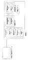
図1は、本発明による非接触/接触両用ICカード制御装置及び携帯電話装置の実施形態を示すブロック図である。
図1に示すように、非接触/接触両用ICカード制御装置である携帯電話1は、リーダライタ11、表示部12、振動発生部13、音声発生部14、CPU等を含む制御部15、記憶部16、切替スイッチ17、携帯側回路18等を備え、無線接続された基地局を介して電波を利用した通信である無線通信を行う通信端末であって、折り畳んで携帯される。携帯電話1は、底面に備える格納部19に非接触/接触両用ICカード2を格納し(後述する図2参照)、接触式で通信を行うことによって非接触/接触両用ICカード2の認証等の諸機能を利用する。
【0022】
リーダライタ11は、接触式で非接触/接触両用ICカード2と通信を行い、情報読み取り、書き込みを行う。リーダライタ11は、携帯電話1の格納部19に接触端子を備え、格納部19に装填された非接触/接触両用ICカード2とこの接触端子を介して通信を行い、電力、クロックの供給、情報の送受信等を行う。
表示部12、振動発生部13及び音声発生部14は、従来の携帯電話が備えるディスプレイ、バイブレータ及びスピーカー等で構築することができ、それぞれ電気信号を画像、振動、音声に変換して出力する。また、表示部12、振動発生部13及び音声発生部14は、携帯側回路18の電力検出部183が所定の電力を検出した場合に、その旨を画像、振動、音声によって通知する非接触通信通知手段である。
【0023】
制御部15は、リーダライタ11、表示部12、振動発生部13、音声発生部14記憶部16、切替スイッチ17、携帯側回路18等が接続され、携帯電話1の情報処理を統括制御する。制御部15は、非接触通信制御部151、接触通信制御部152等を備え、各部は、CPUがメモリ、ハードディスク等である記憶部16に記憶されているプログラムを実行することによって、実現される。
【0024】
非接触通信制御部151は、非接触通信遮断命令を入力した場合に、携帯側回路18の回路スイッチ184を閉じる制御を行い、非接触/接触両用ICカード2のICチップ21が外部装置であるリーダライタ(リーダライタ11とは異なる。以下、このリーダライタを「外部リーダライタ」という。)と非接触式での通信をすることができない非接触通信不能環境へ切り替える。また、非接触通信制御部15は、非接触通信遮断解除命令を入力した場合に、この回路スイッチ184を開ける制御を行うことによって、この非接触通信不能環境を解除する。非接触通信制御部151及び携帯側回路18は、非接触通信不能環境切替手段及び非接触通信可能環境解除手段を構成する。
【0025】
接触通信制御部152は、接触通信遮断命令を入力した場合に、リーダライタ11から非接触/接触両用ICカード2への接触式での電力供給を中止する制御を行い、リーダライタ11がICチップ21と接触式での通信をすることができない接触通信不能環境を提供する接触通信環境切替手段である。また、接触通信制御部152は、接触通信遮断解除命令を入力した場合に、リーダライタ11から非接触/接触両用ICカード2への接触式での電力供給を再開し、接触通信不能環境を解除する接触通信不能環境解除手段である。
【0026】
図2は、本発明による非接触/接触両用ICカード制御装置及び携帯電話装置の実施形態を説明する概略図であって、図2(a)は携帯電話の斜視図、図2(b)は切替スイッチの表面図、図2(c)はIC回路及び携帯側回路のアンテナコイルを示す透視図である。
図2(a)に示すように、格納部19は、カバー191と、その内側に装着部192とを備え、カバー191を携帯電話1から取り外し、装着部192に非接触/接触両用ICカード2を装填し、カバー191を被せてはめ込むことによって、その接触端子がリーダライタ11の接触端子に接触するように保持する保持手段である。
【0027】
図2(b)に示すように、切替スイッチ17は、携帯電話1の側面であって、所持者が携帯電話1を使用する場合に指が当たる位置に設けられている。切替スイッチ17は、所持者が非接触/接触両用ICカード2の通信方式を選択するために切り替えるスイッチであって、非接触遮断、off及び接触遮断の3つのモードを備えている。切替スイッチ17は、接触遮断モードが選択されることによって接触通信遮断命令を入力し、非接触遮断モードが選択されることによって非接触通信遮断命令を入力する通信遮断命令入力手段である。接触遮断モードでは、非接触/接触両用ICカード2が接触式では通信を行うことができない接触式通信不能環境となり、逆に非接触遮断モードは、非接触式では通信を行うことができない非接触通信不能環境となる。offモードは、いずれか一方の通信を行うことが可能な従来の携帯電話と同様の状態となる。
【0028】
また、切替スイッチ17は、非接触遮断モードからoff又は接触遮断モードに切り替えることによって、非接触通信遮断解除命令を入力する非接触通信遮断解除命令入力手段であって、接触遮断モードからoff又は非接触遮断モードに切り替えることによって、接触通信遮断解除命令を入力する接触通信遮断解除命令入力手段である。
従って、切替スイッチ17は、非接触遮断モード及び接触遮断モード間の相互の切り替えによって、通信遮断命令及び非接触通信遮断解除命令、又は、非接触遮断命令及び接触通信遮断解除命令を連係して入力する。
【0029】
図3は、非接触/接触両用ICカード、携帯電話が備える回路を説明する等価回路図であって、図3(a)は非接触/接触両用ICカード2が備えるIC回路20、図3(b)は携帯電話1が備える携帯側回路18を示している。なお、ICチップ21は、抵抗、インダクタンス及びキャパシタンスの各成分を有しているが、説明を簡略化するため、図3において、抵抗Rのみとしてインダクタンス及びキャパシタンスを省略している。また、アンテナコイル22,181及びコンデンサ24,182も同様に、それぞれインダクタンスL及びキャパシタンスCのみとしている。
図3(a)に示すように、IC回路20は、ICチップ21、アンテナコイル22、コンデンサ24等を備え、抵抗R、インダクタンスL及びキャパシタンスCを有する等価回路として表される。IC回路20は、アンテナコイル22及びコンデンサ24が並列に接続された共振回路であるカード側共振回路20sにICチップ21が接続されている。
【0030】
カード側共振回路20sは、外部リーダライタから送信された電磁波と共振するための回路であって、このカード側共振回路20sの周波数f1 は、電磁波の周波数f0 と略同一となるように以下の式に基づいてアンテナコイル22のインダクタンスL及びコンデンサ24のキャパシタンスCが調整されている。
f1 =1/(2π√(LC))≒f0
この周波数f1 が電磁波の周波数f0 の一定誤差範囲内であれば、カード側共振回路20sから誘導起電力がIC回路20に誘起され、ICチップ21が処理を行うために十分な電力が供給される。
【0031】
図3(b)に示すように、携帯電話1が備える携帯側回路18は、アンテナコイル181、コンデンサ182及び電力検出部183、回路スイッチ184等を備え、抵抗R、インダクタンスL及びキャパシタンスCを有する等価回路として表される。携帯側回路18は、回路スイッチ184を介してアンテナコイル181及びコンデンサ182が並列に接続された共振回路である携帯側共振回路18sに電力検出部183が接続されている。
【0032】
携帯側共振回路18sは、回路スイッチ184を閉じた場合に、外部リーダライタから送信された電磁波と共振するための回路であって、この携帯側共振回路20sの周波数f2 は、カード側共振回路20sの周波数f1 と同程度になるようにアンテナコイル181のインダクタンスL及びコンデンサ182のキャパシタンスCが調整されている。また、携帯側共振回路18sは、回路スイッチ184を閉じた場合に、外部リーダライタからの電磁波によって2つのアンテナコイル181,22間に生じる相互インダクタンスによって共振周波数f1 をf0 の一定誤差範囲からずらして、ICチップ21及び外部リーダライタ間の非接触での通信を妨げる。
回路スイッチ184は、制御部15に接続され、非接触通信制御部151によって開閉が制御される。
【0033】
電力検出部183は、携帯側回路20に流れる電流を検出することによって、外部リーダライタから送信された電磁波によって誘起された電力を検出するとともに、前記非接触/接触両用ICカードへ送出される搬送波である電磁波を検出する搬送波検出手段である。電力検出部183には、検流計を用いることができる。電力検出部183は、制御部15に接続され、所定量以上の電流を検出した場合には、その旨の信号を制御部15へ送信する。なお、電力検出部183が検出する下限の電流値及び電力検出部183の抵抗R2は、外部リーダライタからの電磁波によってIC回路20及び携帯側回路18に同時にそれぞれ誘起される電力、ICチップ21が処理を行うために必要な起電力、ICチップ21の抵抗R1等を考慮して設定される。
【0034】
図2(c)に示すように、携帯側回路18のアンテナコイル181は、携帯電話1の内部に非接触/接触両用ICカード2が格納部19に装填された状態で、外部リーダライタからの電磁波によって生じる相互インダクタンスが大きく、カード側共振回路20sの共振周波数f1 に効果的に影響を及ぼすように、その内面がアンテナコイル22の内面に重複し、平行となる位置に設置されている。また、アンテナコイル181は、アンテナコイル22との結合度が高まるように、アンテナコイル22に近いほどよく、隣接することが望ましい。
【0035】
更に、アンテナコイル181は、通信性能の観点から、携帯電話に従来から備えられている機能の妨げとならず、共振周波数f2 の調整が困難にならない等の諸事情を考慮した最大限の大きさで設けられていることが望ましい。
なお、アンテナコイル181は、様々な制限を受けるIC回路20のアンテナコイル22に比べて、非常に大きく設定することが可能である。従って、アンテナコイル181は、アンテナコイル22と同じ外部リーダライタから電磁波を受けた場合であっても、より大きい誘導起電力を得られる等、アンテナコイル22に比べ通信安定性が高い。
【0036】
図4は、本発明による非接触/接触両用ICカード通信制御装置及び携帯電話装置の使用方法を説明する図である。なお、グラデーションは、リーダライタ31から送出された電磁波の強さを示している。
図4に示すように、携帯電話1の所持者は、非接触/接触両用ICカード2を携帯電話1に装填したまま、非接触/接触両用ICカード2の認証機能を利用してゲート開閉システム3のゲート32を通過する等、非接触/接触両用ICカード2の非接触式での通信によって機能を利用したい場合に切替スイッチ17を接触遮断モードに切り替える。
また、所持者は、ゲート開閉システムのリーダライタ31の電磁波が届く範囲内で非接触/接触両用ICカード2の自動決済機能を使って電話をかける等、接触式での通信によって機能を利用したい場合には、非接触遮断モードに切り替える。
【0037】
このように、本実施形態によれば、非接触/接触両用ICカード2を装填した携帯電話1の切替スイッチ17を切り替えることによって、所持者の意志によって接触式又は非接触式での通信方式を選択することができ、利便性を高めることが可能となった。
また、所持者は、切替スイッチ17が非接触遮断モードになっている場合には、表示部12、振動発生部13、音声発生部14等によって外部リーダライタがICチップ21にアクセスしようとしていることを認識することができ、盗聴防止等の防犯を図ることが可能となった。更に、所持者は、非接触/接触両用ICカード2の外部リーダライタとの通信可能範囲を認識することができ、利便性を高めることが可能となった。
【0038】
(変形形態)
以上説明した実施形態に限定されることなく、種々の変形や変更が可能であって、それらも本発明の均等の範囲内である。
例えば、携帯電話1は、非接触通信環境切替手段、接触通信環境切替手段として非接触通信制御部151、接触通信制御部152を備えているが、従来の携帯電話が備える通話遮断ボタン等の既存のスイッチにこの機能を持たせてもよい。
【0039】
非接触/接触通信遮断命令入力手段及び通信遮断解除命令入力手段である切替スイッチ17は、非接触遮断、off及び接触遮断の3つのモードを備え、通信遮断命令及び非接触通信遮断解除命令、又は、非接触遮断命令及び接触通信遮断解除命令を連係して入力するが、非接触遮断及び接触遮断の2つのモードであってもよい。
また、接触遮断命令又は接触遮断解除命令を入力する接触遮断/解除命令入力手段である第1切替スイッチと、非接触遮断命令又は非接触遮断解除命令を入力する非接触遮断/解除命令入力手段である第2スイッチとに分かれ、独立して命令を入力してもよい。
【0040】
携帯側共振回路18sが備えるアンテナコイル181、コンデンサ182は、可変素子であって、携帯電話1の制御部15によってその共振周波数が調整可能であってもよい。共振周波数f2 をカード側共振回路20sの共振周波数f1 と精度よく共振させることによって効果的に非接触通信を妨げることが可能である。
【0041】
携帯電話1は、非接触通信通知手段として、光によって搬送波が検出されたことを通知する通知ランプを備えていてもよい。
【0042】
携帯電話1が備える電力検出部183は、検出する電力の感度を制御部15によって調整可能であってもよい。効果的に非接触通信を妨げるとともに、所持者の利便性を高めることが可能である。
【0043】
【発明の効果】
以上詳しく説明したように、本発明によれば、以下の効果を得ることが可能となった。
(1)非接触通信不能環境を提供する非接触式通信環境切替手段を備えるため、所持者の意志で非接触/接触両用ICカードの接触式通信を可能とすることによって、所持者の利便性を高めること。
(2)接触通信不能環境を提供する接触式通信環境切替手段を備えるため、所持者の意志で非接触/接触両用ICカードの非接触式通信を可能とすることによって、所持者の利便性を高めること。
(3)外部装置から非接触/接触両用ICカードへ送出される搬送波を検出する搬送波検出手段を備えるため、搬送波に対する種々の措置を講じること。
(4)搬送波が検出された旨を通知する非接触通知手段を備えるため、所持者にその旨を通知することによって盗聴防止等の防犯を図ること、また、搬送波の届く範囲を通知することによって利便性を高めること。
【図面の簡単な説明】
【図1】本発明による非接触/接触両用ICカード制御装置及び携帯電話装置の実施形態を示すブロック図である。
【図2】本発明による非接触/接触両用ICカード制御装置及び携帯電話装置の実施形態を説明する概略図である。
【図3】非接触/接触両用ICカード、携帯電話が備える回路を説明する等価回路図である。
【図4】本発明による非接触/接触両用ICカード通信制御装置及び携帯電話装置の使用方法を説明する図である。
【図5】非接触/接触両用ICカードを示すブロック図である。
【符号の説明】
1 携帯電話
2 非接触/接触両用ICカード
3 ゲート開閉システム
11 リーダライタ
12 表示部
13 振動発生部
14 音声発生部
15 制御部
16 記憶部
17 切替スイッチ
18 携帯側回路
19 格納部
20 IC回路
21 ICチップ
151 非接触通信制御部
152 接触通信制御部
183 電力検出部
184 回路スイッチ[0001]
BACKGROUND OF THE INVENTION
The present invention relates to a portable non-contact / contact IC card communication control device that controls communication of a non-contact / contact IC card mounted with an IC chip having both non-contact type and contact type communication means, and this The present invention relates to a mobile phone device that includes a non-contact / contact IC card communication control device and performs wireless communication via a wirelessly connected base station.
[0002]
[Prior art]
Conventionally, portable terminals such as mobile phones and personal digital assistants (PDAs) use non-contact / contact ICs to use various functions such as authentication (including identification) and settlement of non-contact / contact IC cards. Stores cards and communicates in contact. A non-contact / contact IC card is supplied with power via electromagnetic waves and receives data similarly via a non-contact type that transmits data and a terminal formed by a conductor, and similarly receives data. It is an IC card having both contact-type communication methods for electric transmission, and includes a card such as a SIM card that is loaded in a portable terminal and uses its function by contact-type communication.
[0003]
FIG. 5 is a block diagram showing a conventional non-contact / contact IC card.
The non-contact /
[0004]
The
Further, the
When the
The
The
[0005]
The operation
The decoding / modulating
The
The
The
[0006]
[Problems to be solved by the invention]
However, the cellular phone always activates the loaded contactless /
Accordingly, even if the non-contact /
[0007]
Further, when the non-contact /
On the other hand, when another person tries to access information stored in the non-contact /
[0008]
An object of the present invention is to provide a convenient non-contact / contact-use IC card capable of selecting a communication method for a non-contact / contact-use IC card according to the intention of the holder and capable of preventing crimes such as eavesdropping. It is to provide a control device and a mobile phone device.
[0009]
[Means for Solving the Problems]
The present invention solves the above problems by the following means. In addition, in order to make an understanding easy, it attaches | subjects and demonstrates the code | symbol corresponding to embodiment of this invention, but it is not limited to this..
[0010]
Claim1The invention ofA holding means (19) for holding a non-contact / contact IC card (2) having an IC chip (21) that communicates with the external device (3) in a non-contact manner or in a contact manner, and a non-contact communication cutoff command are input. When the non-contact communication cutoff command input means (17) and the non-contact communication cutoff command input means input the non-contact communication cutoff command, non-contact communication is performed between the IC chip and the external device. Non-contact communication impossible environment switching means (18, 151) for switching to a non-contact communication impossible environment that cannot be performed;Contact communication means (11) for communicating with the IC chip in a contact manner, contact communication cutoff command input means (17) for inputting a contact communication cutoff command, and the contact communication cutoff command by the contact communication cutoff command input means. A contact communication disabled environment switching unit (152) for switching to a contact communication disabled environment incapable of performing communication in a contact manner between the contact communication unit and the IC chip when input,The non-contact communication impossible environment switching means includes a second resonance circuit (18s) that resonates with a resonance frequency of the first resonance circuit (20s) included in the non-contact / contact IC card, and the second And a switch that opens and closes the circuit of the second resonance circuit, and the non-contact communication impossible environment switching means performs non-contact communication by closing the switch. Therefore, non-contact communication is disabled by shifting the resonance frequency of the first resonance circuit from the carrier frequency, which resonates with the carrier frequency that is the frequency of the carrier transmitted from the external device to the contactless / contact IC card. Switch to environmentA portable non-contact / contact IC card communication control device (1).
[0011]
Claim2The invention of claim1In the non-contact / contact-use IC card communication control device described above, the non-contact communication cutoff release command or the communication cutoff release command input means (17) for inputting a contact communication cutoff release command and the communication cutoff release command input means Communication enable environment switching means (18) that switches the contactless communication disabled environment or the contact communication disabled environment to a contactless communication enabled environment or a contact communication enabled environment when a contact communication disconnection cancel command or a contact communication disconnection cancel command is input. , 151, 152). A non-contact / contact-use IC card communication control device (1).
[0012]
Claim3The invention of claim2In the non-contact / contact-use IC card communication control device according to claim 1, the communication cutoff release command input means is the non-contact communication cutoff command or the contact by the non-contact communication cutoff command input means or the contact communication cutoff command input means. A contactless / contact-use IC card communication control device (1), wherein the contact communication cutoff cancellation command or the contactless communication cutoff cancellation command is input in conjunction with an input of a communication cutoff command.
[0016]
Claim4The invention of claim 1 to claim 13The contactless / contact-use IC card communication control device according to any one of the preceding claims, wherein the noncontact communication disabled environment switching unit switches the noncontact communication disabled environment to the noncontact communication disabled environment. A non-contact / contact-use IC card communication control device (1) comprising carrier-carrier detection means (183) for detecting a carrier sent to the contact / contact-use IC card.
[0017]
Claim5The invention of claim4In the non-contact / contact IC card communication control device according to claim 1, the carrier wave detecting means is an element connected to the second resonance circuit, and is induced in the second resonance circuit by a carrier wave of the external device. The non-contact / contact-use IC card communication control device (1) is characterized in that it is a power detection unit (183) for detecting the detected power.
[0018]
Claim6The invention of claim4Or claim5In the non-contact / contact-use IC card communication control device according to claim 1, provided with non-contact communication notification means (12, 13, 14) for notifying that when the carrier wave is detected by the carrier wave detection means, 1 is a non-contact / contact-use IC card communication control device (1).
[0019]
Claim7The present invention is a mobile phone device that performs wireless communication via a wirelessly connected base station.6A mobile phone device (1) comprising the non-contact / contact-use IC card communication control device according to any one of the above.
[0020]
Claim8The invention of claim7The mobile phone device according to claim 1, further comprising a display unit (12) for notifying information by image, sound and / or vibration, a sound output unit (14) and / or a vibration generating unit (13), The contact communication notification means includes the display unit, the audio output unit, and / or the vibration generation unit.
[0021]
DETAILED DESCRIPTION OF THE INVENTION
Hereinafter, embodiments of the present invention will be described in more detail with reference to the drawings.
(Embodiment)
FIG. 1 is a block diagram showing an embodiment of a non-contact / contact IC card control device and a mobile phone device according to the present invention.
As shown in FIG. 1, a mobile phone 1 which is a non-contact / contact-use IC card control device includes a reader /
[0022]
The reader /
The display unit 12, the
[0023]
The control unit 15 is connected to the reader /
[0024]
When the non-contact communication control unit 151 inputs a non-contact communication cutoff command, the circuit switch of the portable circuit 18184Is controlled so that the
[0025]
The contact communication control unit 152 performs control to stop the contact-type power supply from the reader /
[0026]
FIG. 2 is a schematic diagram illustrating an embodiment of a non-contact / contact IC card control device and a mobile phone device according to the present invention. FIG. 2 (a) is a perspective view of the mobile phone, and FIG. FIG. 2C is a perspective view showing the IC coil and the antenna coil of the portable circuit.
As shown in FIG. 2A, the
[0027]
As shown in FIG. 2 (b), the
[0028]
The change-
Accordingly, the
[0029]
3 is an equivalent circuit diagram for explaining a circuit provided in the non-contact / contact IC card and the mobile phone. FIG. 3A shows an
As shown in FIG. 3A, the
[0030]
The card
f1= 1 / (2π√ (LC)) ≈f0
This frequency f1Is the frequency f of the electromagnetic wave0Is within a certain error range, induced electromotive force is induced in the
[0031]
As shown in FIG. 3B, the
[0032]
The portable
The
[0033]
The
[0034]
As shown in FIG. 2C, the
[0035]
Furthermore, the
The
[0036]
FIG. 4 is a diagram for explaining a method of using the non-contact / contact-use IC card communication control device and the mobile phone device according to the present invention. Note that the gradation indicates the strength of the electromagnetic wave transmitted from the reader /
As shown in FIG. 4, the holder of the mobile phone 1 uses the authentication function of the non-contact /
In addition, the owner wants to use the function by contact type communication such as making a call using the automatic settlement function of the non-contact /
[0037]
As described above, according to the present embodiment, by switching the change-
In addition, when the
[0038]
(Deformation)
The present invention is not limited to the embodiment described above, and various modifications and changes are possible, and these are also within the equivalent scope of the present invention.
For example, the mobile phone 1 includes a non-contact communication environment switching unit and a non-contact communication control unit 151 and a contact communication control unit 152 as a contact communication environment switching unit. The switch may have this function.
[0039]
The
Also, a first changeover switch that is a contact block / release command input means for inputting a contact block command or a contact block cancel command, and a non-contact block / release command input unit that inputs a non-contact block command or a non-contact block cancel command It may be divided into a second switch and an instruction may be input independently.
[0040]
The
[0041]
The mobile phone 1 may include a notification lamp that notifies that a carrier wave has been detected by light as non-contact communication notification means.
[0042]
The
[0043]
【The invention's effect】
As described above in detail, according to the present invention, the following effects can be obtained.
(1) Since a contactless communication environment switching means for providing a contactless communication disabled environment is provided, it is possible for the holder to make contactless communication with a noncontact / contact IC card by the owner's will. To increase.
(2) Since contact-type communication environment switching means for providing an environment incapable of contact communication is provided, non-contact / contact-type IC card non-contact communication is possible at the will of the owner, thereby improving the convenience of the owner. To raise.
(3) Since a carrier wave detecting means for detecting a carrier wave sent from the external device to the non-contact / contact IC card is provided, various measures for the carrier wave are taken.
(4) Since contactless notification means for notifying that a carrier wave has been detected is provided, it is intended to prevent eavesdropping and the like by notifying the owner to that effect, and by notifying the range where the carrier wave reaches Increase convenience.
[Brief description of the drawings]
FIG. 1 is a block diagram showing an embodiment of a non-contact / contact IC card control device and a mobile phone device according to the present invention.
FIG. 2 is a schematic diagram illustrating an embodiment of a non-contact / contact IC card control device and a mobile phone device according to the present invention.
FIG. 3 is an equivalent circuit diagram illustrating a circuit included in a non-contact / contact IC card and a mobile phone.
FIG. 4 is a diagram for explaining a method of using a non-contact / contact IC card communication control device and a mobile phone device according to the present invention.
FIG. 5 is a block diagram showing a non-contact / contact IC card.
[Explanation of symbols]
1 Mobile phone
2 IC card for non-contact / contact use
3 Gate opening and closing system
11 Reader / Writer
12 Display section
13 Vibration generator
14 Sound generator
15 Control unit
16 Memory unit
17 changeover switch
18 Mobile circuit
19 Storage
20 IC circuit
21 IC chip
151 Non-contact communication control unit
152 Contact communication control unit
183 Power detection unit
184 circuit switch
Claims (8)
非接触通信遮断命令を入力する非接触通信遮断命令入力手段と、
前記非接触通信遮断命令入力手段によって前記非接触通信遮断命令を入力した場合に、前記ICチップ及び前記外部装置間における非接触式での通信を行うことが不可能な非接触通信不能環境へ切り替える非接触通信不能環境切替手段と、
前記ICチップと接触方式で通信を行う接触通信手段と、
接触通信遮断命令を入力する接触通信遮断命令入力手段と、
前記接触通信遮断命令入力手段によって前記接触通信遮断命令を入力した場合に、前記接触通信手段及び前記ICチップ間における接触方式での通信を行うことが不可能な接触通信不能環境へ切り替える接触通信不能環境切替手段と、
を備え、
前記非接触通信不能環境切替手段は、
前記非接触/接触両用ICカードが有する第1の共振回路の共振周波数と共振する第2の共振回路と、
前記第2の共振回路中に設けられ、前記第2の共振回路の回路を開閉するスイッチと、
を有し、
前記非接触通信不能環境切替手段は、前記スイッチを閉じることにより、非接触式で通信を行うために前記外部装置から前記非接触/接触両用ICカードへ送出される搬送波の周波数である搬送波周波数と共振する、前記第1の共振回路の共振周波数を前記搬送波周波数からずらすことによって非接触通信不能環境へ切り替える携帯可能な非接触/接触両用ICカード通信制御装置。Holding means for holding a non-contact / contact IC card comprising an IC chip that communicates with an external device in a non-contact or contact manner;
Non-contact communication cutoff command input means for inputting a non-contact communication cutoff command;
When the non-contact communication cutoff command input means inputs the non-contact communication cutoff command, switching to a non-contact communication impossible environment where it is impossible to perform non-contact communication between the IC chip and the external device Non-contact communication impossible environment switching means,
Contact communication means for communicating with the IC chip in a contact manner;
A contact communication cutoff command input means for inputting a contact communication cutoff command;
When the contact communication cutoff command is input by the contact communication cutoff command input means, the contact communication cannot be switched to an environment incapable of performing contact communication between the contact communication means and the IC chip. Environmental switching means;
With
The non-contact communication impossible environment switching means,
A second resonance circuit that resonates with a resonance frequency of the first resonance circuit of the non-contact / contact IC card;
A switch provided in the second resonance circuit for opening and closing the circuit of the second resonance circuit;
Have
The non-contact communication impossible environment switching means includes a carrier frequency that is a frequency of a carrier transmitted from the external device to the non-contact / contact IC card in order to perform non-contact communication by closing the switch. A portable non-contact / contact IC card communication control device for switching to a non-contact communication impossible environment by shifting the resonance frequency of the first resonance circuit that resonates from the carrier frequency.
非接触通信遮断解除命令又は接触通信遮断解除命令を入力する通信遮断解除命令入力手段と、
前記通信遮断解除命令入力手段によって前記非接触通信遮断解除命令又は接触通信遮断解除命令が入力された場合に、前記非接触通信不能環境又は前記接触通信不能環境を非接触通信可能環境又は接触通信可能環境へ切り替える通信可能環境切替手段とを備えること、
を特徴とする非接触/接触両用ICカード通信制御装置。In the non-contact / contact-use IC card communication control device according to claim 1,
A communication cutoff release command input means for inputting a non-contact communication cutoff release command or a contact communication cutoff release command;
When the non-contact communication cutoff cancellation command or the contact communication cutoff cancellation command is input by the communication cutoff cancellation command input means, the non-contact communication disable environment or the contact communication disable environment is non-contact communication enable environment or contact communication possible A communication-capable environment switching means for switching to the environment,
A non-contact / contact-use IC card communication control device.
前記通信遮断解除命令入力手段は、前記非接触通信遮断命令入力手段又は前記接触通信遮断命令入力手段による前記非接触通信遮断命令又は前記接触通信遮断命令の入力と連係して前記接触通信遮断解除命令又は前記非接触通信遮断解除命令を入力すること、
を特徴とする非接触/接触両用ICカード通信制御装置。In the non-contact / contact-use IC card communication control device according to claim 2,
The communication cutoff release command input means is connected to the non-contact communication cutoff command input means or the contact communication cutoff command input means in connection with the input of the non-contact communication cutoff command or the contact communication cutoff command. Or inputting the non-contact communication cutoff release command,
A non-contact / contact-use IC card communication control device.
前記非接触通信不能環境切替手段によって前記非接触通信不能環境へ切り替えられている場合に、前記外部装置から前記非接触/接触両用ICカードへ送出される搬送波を検出する搬送波検出手段を備えること、
を特徴とする非接触/接触両用ICカード通信制御装置。In the non-contact / contact both-use IC card communication control apparatus according to any one of claims 1 to 3 ,
A carrier detection means for detecting a carrier sent from the external device to the non-contact / contact IC card when the non-contact communication impossible environment switching means is switched to the non-contact communication impossible environment;
A non-contact / contact-use IC card communication control device.
前記搬送波検出手段は、前記第2の共振回路に接続された素子であり、前記外部装置の搬送波によって前記第2の共振回路に誘起された電力を検出する電力検出部であること、
を特徴とする非接触/接触両用ICカード通信制御装置。In the non-contact / contact both-use IC card communication control device according to claim 4 ,
The carrier wave detection means is an element connected to the second resonance circuit, and is a power detection unit for detecting power induced in the second resonance circuit by a carrier wave of the external device;
A non-contact / contact-use IC card communication control device.
前記搬送波検出手段により前記搬送波が検出された場合に、その旨を通知する非接触通信通知手段を備えること、
を特徴とする非接触/接触両用ICカード通信制御装置。In the non-contact / contact IC card communication control device according to claim 4 or 5 ,
When the carrier wave is detected by the carrier wave detection means, comprising a non-contact communication notification means for notifying that effect,
A non-contact / contact-use IC card communication control device.
請求項1から請求項6までのいずれか1項に記載の非接触/接触両用ICカード通信制御装置を備えること、
を特徴とする携帯電話装置。A mobile phone device that performs wireless communication via a wirelessly connected base station,
A non-contact / contact IC card communication control device according to any one of claims 1 to 6 , comprising:
A mobile phone device characterized by the above.
情報を画像、音声、及び/又は、振動で通知する表示部、音声出力部、及び/又は、振動発生部を備え、
前記非接触通信通知手段は、前記表示部、前記音声出力部、及び/又は、前記振動発生部を含むこと、
を特徴とする携帯電話装置。The mobile phone device according to claim 7 , wherein
A display unit for notifying information by image, sound, and / or vibration, a sound output unit, and / or a vibration generating unit;
The non-contact communication notification means includes the display unit, the audio output unit, and / or the vibration generation unit;
A mobile phone device characterized by the above.
Priority Applications (1)
| Application Number | Priority Date | Filing Date | Title |
|---|---|---|---|
| JP2002022621A JP4022073B2 (en) | 2002-01-31 | 2002-01-31 | Non-contact / contact IC card communication control device and mobile phone device |
Applications Claiming Priority (1)
| Application Number | Priority Date | Filing Date | Title |
|---|---|---|---|
| JP2002022621A JP4022073B2 (en) | 2002-01-31 | 2002-01-31 | Non-contact / contact IC card communication control device and mobile phone device |
Publications (2)
| Publication Number | Publication Date |
|---|---|
| JP2003223618A JP2003223618A (en) | 2003-08-08 |
| JP4022073B2 true JP4022073B2 (en) | 2007-12-12 |
Family
ID=27745569
Family Applications (1)
| Application Number | Title | Priority Date | Filing Date |
|---|---|---|---|
| JP2002022621A Expired - Fee Related JP4022073B2 (en) | 2002-01-31 | 2002-01-31 | Non-contact / contact IC card communication control device and mobile phone device |
Country Status (1)
| Country | Link |
|---|---|
| JP (1) | JP4022073B2 (en) |
Families Citing this family (9)
| Publication number | Priority date | Publication date | Assignee | Title |
|---|---|---|---|---|
| TW200608402A (en) * | 2004-08-20 | 2006-03-01 | Renesas Tech Corp | Semiconductor integrated device, and IC card and portable information terminal using the semiconductor integrated device |
| JP4523449B2 (en) * | 2005-02-23 | 2010-08-11 | 日本電信電話株式会社 | Key service method, system and program thereof |
| KR101053185B1 (en) | 2005-02-24 | 2011-08-01 | 삼성전자주식회사 | Smart card and its mixed mode control method |
| JP4508948B2 (en) * | 2005-06-01 | 2010-07-21 | シャープ株式会社 | Mobile terminal device |
| JP5114029B2 (en) * | 2006-07-11 | 2013-01-09 | Necカシオモバイルコミュニケーションズ株式会社 | Portable terminal device and program |
| KR100766607B1 (en) | 2006-07-28 | 2007-10-12 | 주식회사 케이티프리텔 | Smart card unified communication functions of contact type and non-contact type and operation controlling method thereof |
| JP4554664B2 (en) * | 2007-11-26 | 2010-09-29 | 富士通株式会社 | Information display system and display element driving method |
| JP5619414B2 (en) * | 2009-12-25 | 2014-11-05 | 三洋電機株式会社 | Wireless communication device |
| JP6245560B2 (en) * | 2015-01-28 | 2017-12-13 | パナソニックIpマネジメント株式会社 | Payment terminal device |
-
2002
- 2002-01-31 JP JP2002022621A patent/JP4022073B2/en not_active Expired - Fee Related
Also Published As
| Publication number | Publication date |
|---|---|
| JP2003223618A (en) | 2003-08-08 |
Similar Documents
| Publication | Publication Date | Title |
|---|---|---|
| JP4167649B2 (en) | Folding type mobile radio telephone with built-in non-contact IC card function | |
| JP5009361B2 (en) | Portable radio | |
| JP5153501B2 (en) | COMMUNICATION DEVICE AND COMMUNICATION DEVICE CONTROL METHOD | |
| KR100750436B1 (en) | Wireless communication terminal | |
| US8219143B2 (en) | Mobile radio device | |
| JP5622612B2 (en) | Portable electronic devices | |
| WO2006025229A1 (en) | Semiconductor integrated circuit and wireless communication device | |
| JP2007166379A (en) | Loop antenna and electronic apparatus with same | |
| JP2007088661A (en) | Information processing apparatus and loop antenna | |
| JP4022073B2 (en) | Non-contact / contact IC card communication control device and mobile phone device | |
| JP2010514307A (en) | Radio frequency radio wave communication local interface between mobile phone and contactless reader device | |
| KR20080023712A (en) | Nfc function control device for mobile terminal having id card and nfc chip | |
| EP2752999B1 (en) | Mobile wireless communications device including NFC antenna matching control circuit and associated methods | |
| JP5287110B2 (en) | Wireless device | |
| JP2003228693A (en) | Ic card | |
| WO2008029461A1 (en) | Non-contact ic device | |
| JP2008022469A (en) | Mobile terminal device | |
| JPWO2008120757A1 (en) | Portable radio | |
| JP2004048251A (en) | Portable terminal apparatus | |
| JP2006304039A (en) | Portable terminal | |
| JP5330701B2 (en) | Battery pack and portable electronic device | |
| WO2001024108A1 (en) | Noncontact ic card capable of inhibiting data transmission | |
| KR20160068068A (en) | Terminal device cover and radio frequency commuication device including radio frequency authentication module | |
| JP2006244214A (en) | Non-contact ic card adjustment method, non-contact ic card adjustment system, non-contact ic card and mobile communication equipment | |
| JP4694978B2 (en) | Folding portable terminal with non-contact IC card |
Legal Events
| Date | Code | Title | Description |
|---|---|---|---|
| A621 | Written request for application examination |
Free format text: JAPANESE INTERMEDIATE CODE: A621 Effective date: 20050124 |
|
| RD02 | Notification of acceptance of power of attorney |
Free format text: JAPANESE INTERMEDIATE CODE: A7422 Effective date: 20061116 |
|
| A977 | Report on retrieval |
Free format text: JAPANESE INTERMEDIATE CODE: A971007 Effective date: 20061226 |
|
| A131 | Notification of reasons for refusal |
Free format text: JAPANESE INTERMEDIATE CODE: A131 Effective date: 20070116 |
|
| A521 | Request for written amendment filed |
Free format text: JAPANESE INTERMEDIATE CODE: A523 Effective date: 20070319 |
|
| A131 | Notification of reasons for refusal |
Free format text: JAPANESE INTERMEDIATE CODE: A131 Effective date: 20070410 |
|
| A521 | Request for written amendment filed |
Free format text: JAPANESE INTERMEDIATE CODE: A523 Effective date: 20070606 |
|
| TRDD | Decision of grant or rejection written | ||
| A01 | Written decision to grant a patent or to grant a registration (utility model) |
Free format text: JAPANESE INTERMEDIATE CODE: A01 Effective date: 20070925 |
|
| A61 | First payment of annual fees (during grant procedure) |
Free format text: JAPANESE INTERMEDIATE CODE: A61 Effective date: 20070928 |
|
| FPAY | Renewal fee payment (event date is renewal date of database) |
Free format text: PAYMENT UNTIL: 20101005 Year of fee payment: 3 |
|
| R150 | Certificate of patent or registration of utility model |
Free format text: JAPANESE INTERMEDIATE CODE: R150 |
|
| FPAY | Renewal fee payment (event date is renewal date of database) |
Free format text: PAYMENT UNTIL: 20111005 Year of fee payment: 4 |
|
| FPAY | Renewal fee payment (event date is renewal date of database) |
Free format text: PAYMENT UNTIL: 20121005 Year of fee payment: 5 |
|
| FPAY | Renewal fee payment (event date is renewal date of database) |
Free format text: PAYMENT UNTIL: 20131005 Year of fee payment: 6 |
|
| LAPS | Cancellation because of no payment of annual fees |