JP4020552B2 - Solar cell packaging structure - Google Patents
Solar cell packaging structure Download PDFInfo
- Publication number
- JP4020552B2 JP4020552B2 JP34011599A JP34011599A JP4020552B2 JP 4020552 B2 JP4020552 B2 JP 4020552B2 JP 34011599 A JP34011599 A JP 34011599A JP 34011599 A JP34011599 A JP 34011599A JP 4020552 B2 JP4020552 B2 JP 4020552B2
- Authority
- JP
- Japan
- Prior art keywords
- solar cell
- output terminal
- adhesive
- plate
- packaging structure
- Prior art date
- Legal status (The legal status is an assumption and is not a legal conclusion. Google has not performed a legal analysis and makes no representation as to the accuracy of the status listed.)
- Expired - Lifetime
Links
- 238000004806 packaging method and process Methods 0.000 title claims description 9
- 239000000853 adhesive Substances 0.000 claims description 19
- 230000001070 adhesive effect Effects 0.000 claims description 19
- 230000001681 protective effect Effects 0.000 claims description 7
- 239000000758 substrate Substances 0.000 claims description 7
- 239000002184 metal Substances 0.000 claims description 3
- 229910052751 metal Inorganic materials 0.000 claims description 3
- XUIMIQQOPSSXEZ-UHFFFAOYSA-N Silicon Chemical compound [Si] XUIMIQQOPSSXEZ-UHFFFAOYSA-N 0.000 claims 1
- 229910052710 silicon Inorganic materials 0.000 claims 1
- 239000010703 silicon Substances 0.000 claims 1
- 239000000463 material Substances 0.000 description 8
- 238000005259 measurement Methods 0.000 description 7
- WABPQHHGFIMREM-UHFFFAOYSA-N lead(0) Chemical compound [Pb] WABPQHHGFIMREM-UHFFFAOYSA-N 0.000 description 4
- 238000010248 power generation Methods 0.000 description 4
- RYGMFSIKBFXOCR-UHFFFAOYSA-N Copper Chemical compound [Cu] RYGMFSIKBFXOCR-UHFFFAOYSA-N 0.000 description 3
- 230000005611 electricity Effects 0.000 description 3
- 230000003068 static effect Effects 0.000 description 3
- 229910052802 copper Inorganic materials 0.000 description 2
- 239000010949 copper Substances 0.000 description 2
- 230000007547 defect Effects 0.000 description 2
- 239000011521 glass Substances 0.000 description 2
- 238000005476 soldering Methods 0.000 description 2
- 238000011179 visual inspection Methods 0.000 description 2
- KXGFMDJXCMQABM-UHFFFAOYSA-N 2-methoxy-6-methylphenol Chemical compound [CH]OC1=CC=CC([CH])=C1O KXGFMDJXCMQABM-UHFFFAOYSA-N 0.000 description 1
- 229910021417 amorphous silicon Inorganic materials 0.000 description 1
- 239000011230 binding agent Substances 0.000 description 1
- 229920005549 butyl rubber Polymers 0.000 description 1
- 230000000694 effects Effects 0.000 description 1
- 238000010438 heat treatment Methods 0.000 description 1
- 238000007689 inspection Methods 0.000 description 1
- 239000002245 particle Substances 0.000 description 1
- 238000000059 patterning Methods 0.000 description 1
- 229920001568 phenolic resin Polymers 0.000 description 1
- 239000005011 phenolic resin Substances 0.000 description 1
- 229920005989 resin Polymers 0.000 description 1
- 239000011347 resin Substances 0.000 description 1
- 238000007650 screen-printing Methods 0.000 description 1
- 230000000007 visual effect Effects 0.000 description 1
Images


Classifications
-
- Y—GENERAL TAGGING OF NEW TECHNOLOGICAL DEVELOPMENTS; GENERAL TAGGING OF CROSS-SECTIONAL TECHNOLOGIES SPANNING OVER SEVERAL SECTIONS OF THE IPC; TECHNICAL SUBJECTS COVERED BY FORMER USPC CROSS-REFERENCE ART COLLECTIONS [XRACs] AND DIGESTS
- Y02—TECHNOLOGIES OR APPLICATIONS FOR MITIGATION OR ADAPTATION AGAINST CLIMATE CHANGE
- Y02E—REDUCTION OF GREENHOUSE GAS [GHG] EMISSIONS, RELATED TO ENERGY GENERATION, TRANSMISSION OR DISTRIBUTION
- Y02E10/00—Energy generation through renewable energy sources
- Y02E10/50—Photovoltaic [PV] energy
Landscapes
- Photovoltaic Devices (AREA)
Description
【0001】
【発明の属する技術分野】
本発明は、太陽電池の包装構造に関する。
【0002】
【従来の技術】
従来の太陽電池の出荷構造としての収納構造が、例えば、実公平5−30368号に開示されている。この収納構造は、複数の凹状収納部を有するパレットを用いるものであり、凹状収納部に、板状の太陽電池を収納するものである。
【0003】
【発明が解決しようとする課題】
このような従来の収納構造においては、出荷の前、または、収納構造を受け取った後、太陽電池が適正に動作するかどうかについて太陽電池の特性を測定する場合には、一つ一つ個別に測定する必要があった。
【0004】
本発明は、このような問題点を解決するために成されたものであり、太陽電池の特性測定が容易にできる包装構造を提供することを目的とする。
【0005】
【課題を解決するための手段】
本発明の構成は、光入射面の反対面に出力端子を有する板状の太陽電池と、前記太陽電池の前記反対面において接着材を用いて着脱自在に、前記太陽電池を固定する板体とを有する包装構造であって、前記板体に前記太陽電池が固定された状態で、前記出力端子に対向する前記板体の部分に、開口を有することを特徴とする。
【0006】
更に、本発明の構成は、前記板体より前記太陽電池を分離したとき、前記接着材が前記太陽電池に付着していることを特徴とする。
【0007】
【発明の実施の形態】
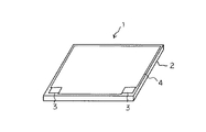
本発明の一実施例を、図1〜4を用いて詳細に説明する。図1は包装する太陽電池1を示す斜視図であり、2がガラス等の絶縁透光性基板、3は透明導電膜、非晶質シリコン膜及び金属電極膜からなる発電膜からの出力を導出する出力端子、4は発電膜を被い出力端子2を露出させる樹脂材料等からなる保護膜である。出力端子3の材質は、透明導電膜、金属膜、銅ペースト膜等が採用できる。ここで、銅ペースト膜は、ガラス基板上で通常の半田付け作業ができるもので、フェノール系樹脂をバインダーとして、粒径約5〜7μmの銅粉末を重量比約90%で混入したものからなり、スクリーン印刷によるパターニング後、加熱処理により硬化される。この太陽電池1においては、光入射面が基板2の表面(図1においては下面)となり、この反対面に出力端子3が位置することになる。
【0008】
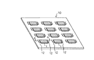
図2は本実施例の包装構造を示す斜視図であり、10は、プラスチック、ボール紙等からなる矩形板状の板体であり、図に示すように、複数の太陽電池1、1、1・・・は、光入射面である基板2を上にした状態で、固定されている。
【0009】
そして、図3(=図2におけるA−A断面図)に示すように、太陽電池1は、その反対面である保護膜4上と、板体10表面上の間に、ブチルゴム等の接着材11を用いて固定されている。ここで、接着材11は、太陽電池1が着脱自在に接着できる程度に、微接着性のものを利用する。
【0010】
また、太陽電池1の出力端子3に対向する板体11の部分に、開口12、12・・・が位置する形状を、板体10は有している。
【0011】
本実施例は、以上の包装構造であって、太陽電池1の出力端子3、3が、板体10の開口12、12に位置して、露出されているので、特性測定を行う場合には、出力端子3、3に測定端子を当てて、太陽電池1の光入射面にモニター光を入射させて、特性測定を行うことができる。同様にして、複数の他の太陽電池1、1、1・・・についても、特性測定ができる。つまり、包装状態のままで、特性測定ができるので、従来のように、一つ一つ個別に測定する必要がないので、測定に係わる作業が容易である。また、太陽電池1の光入射面が上を向いているので、目視による、太陽電池1の基板2表面上のキズ、欠け等の外観不良の検査を効率よく行うことができる。
【0012】
そして、図2の状態の包装構造を複数用意し、図4のように、積み重ねた状態で、出荷することができる。図4の積み重ねた収納状態においては、従来のパレットを用いる収納構造と比較して、単位体積あたりに収納される太陽電池の数が大きい。
【0013】
更には、本実施例の包装構造を受け取ったユーザーは、上述の出荷前と同様に、特性測定と、外観検査を効率良く行うことができる。そして、接着材11は微接着性のものであり、太陽電池1を板体10より容易に、分離することができる。
【0014】
また、本実施例においては、太陽電池1を分離するとき、接着材6が太陽電池1の保護膜4側に付着するように、板体10の材質及び表面状態、接着材11の種類、太陽電池1の保護膜4の種類を選択することができる。例えば、本実施例においては、板体10に、表面が滑らかなプラスチック材料を採用して、太陽電池1側に接着材11が付着することにより、太陽電池1を電卓等の電子機器に組み込んだ場合、接着材11にて電子機器内部に、太陽電池1を接着して固定することができる。
【0015】
更に、本実施例の輸送中においては、太陽電池1が接着材11を介して板体10に固定されていることより、板体11に対して太陽電池1が振動することが少ないので、静電気が発生することが少ない。よって、静電気により、発電膜のショート等の損傷が発生することを抑えることができる。
【0016】
そして、太陽電池1の出力端子3は、開口12に位置することになるので、輸送中に振動して出力端子3が擦れることなく、クリーンな状態を保つことができる。よって、輸送後、出力端子3にリード線を半田付けする場合、出力端子が擦れて汚れ、半田がのらない、あるいは、半田付け強度が弱い等の問題が発生することが少ない。また、出力端子3に、いわゆる、ヒートシールを用いて電気接続を行う場合においても、出力端子が擦れて汚れていないので、ヒートシールを熱圧着して、良好な状態で電気的、強度的に接続できる。
【0017】
また、図2に示す本実施例の包装構造においては、太陽電池1の出力端子3が、開口12に位置することになるので、開口12を通じて、出力端子3にリード線を接続するなら、複数の太陽電池に効率良く、リード線を接続することも可能である。
【0018】
【発明の効果】
本発明は、太陽電池の出力端子が、板体の開口に位置して、露出されているので、包装状態のままで、特性測定が容易にでき、従来のように、一つ一つ個別に測定する必要がないので、測定に係わる作業が容易である。また、太陽電池の光入射面が上を向いているので、目視による、太陽電池の基板表面上のキズ、欠け等の外観不良の検査を効率よく行うことができる。
【0019】
更には、輸送中においては、太陽電池が接着材を介して板体に固定されていることより、板体に対して太陽電池が振動することが少ないので、静電気が発生することが少ない。よって、静電気により、発電膜のショート等の損傷が発生することを抑えることができる。そして、太陽電池の出力端子は、開口に位置することになるので、輸送中に振動して出力端子が擦れることなく、クリーンな状態を保つことができる。よって、輸送後、出力端子にリード線を半田付け、またはヒートシールを熱圧着する場合、良好な状態で電気的、強度的に接続できる。
【0020】
また、板体より太陽電池を分離したとき、接着材が太陽電池に付着しているので、太陽電池を電卓等の電子機器に組み込んだ場合、接着材にて電子機器内部に、太陽電池を接着して固定することができる。
【図面の簡単な説明】
【図1】本発明の太陽電池を示す斜視図である。
【図2】本発明の一実施例を示す斜視図である。
【図3】図2のA−A断面図である。
【図4】本発明の一実施例を重ねた状態を示す斜視図である。
【符号の説明】
1 太陽電池
3 出力端子
10 板体
11 接着材
12 開口[0001]
BACKGROUND OF THE INVENTION
The present invention relates to a solar cell packaging structure.
[0002]
[Prior art]
A storage structure as a conventional shipping structure for solar cells is disclosed in, for example, Japanese Utility Model Publication No. 5-30368. This storage structure uses a pallet having a plurality of concave storage portions, and stores plate-like solar cells in the concave storage portions.
[0003]
[Problems to be solved by the invention]
In such a conventional storage structure, when measuring the characteristics of the solar cell about whether the solar cell operates properly before shipment or after receiving the storage structure, one by one. It was necessary to measure.
[0004]
The present invention has been made to solve such problems, and an object thereof is to provide a packaging structure capable of easily measuring the characteristics of a solar cell.
[0005]
[Means for Solving the Problems]
The configuration of the present invention includes a plate-like solar cell having an output terminal on the opposite surface of the light incident surface, and a plate body for fixing the solar cell detachably using an adhesive on the opposite surface of the solar cell; In the state where the solar cell is fixed to the plate body, an opening is provided in a portion of the plate body facing the output terminal.
[0006]
Furthermore, the configuration of the present invention is characterized in that when the solar cell is separated from the plate body, the adhesive is attached to the solar cell.
[0007]
DETAILED DESCRIPTION OF THE INVENTION
An embodiment of the present invention will be described in detail with reference to FIGS. FIG. 1 is a perspective view showing a
[0008]
FIG. 2 is a perspective view showing the packaging structure of the present embodiment.
[0009]
As shown in FIG. 3 (= A-A cross-sectional view in FIG. 2), the
[0010]
Moreover, the
[0011]
In this embodiment, the packaging structure is as described above, and the
[0012]
2 can be prepared and shipped in a stacked state as shown in FIG. In the stacked storage state of FIG. 4, the number of solar cells stored per unit volume is large as compared with a storage structure using a conventional pallet.
[0013]
Furthermore, the user who has received the packaging structure of the present embodiment can efficiently perform the characteristic measurement and the appearance inspection in the same manner as before shipping. The
[0014]
Further, in this embodiment, when the
[0015]
Further, during the transportation of the present embodiment, since the
[0016]
And since the
[0017]
Further, in the packaging structure of the present embodiment shown in FIG. 2, the
[0018]
【The invention's effect】
In the present invention, since the output terminal of the solar cell is located at the opening of the plate body and is exposed, the characteristic measurement can be easily performed in the packaged state. Since there is no need to measure, work related to measurement is easy. Further, since the light incident surface of the solar cell faces upward, it is possible to efficiently inspect visual defects such as scratches and chips on the substrate surface of the solar cell by visual inspection.
[0019]
Furthermore, during transportation, since the solar cell is fixed to the plate body via the adhesive, the solar cell is less likely to vibrate with respect to the plate body, so that static electricity is hardly generated. Therefore, it is possible to suppress the occurrence of damage such as a short circuit of the power generation film due to static electricity. And since the output terminal of a solar cell will be located in opening, it can maintain a clean state, without vibrating during output and rubbing an output terminal. Therefore, when the lead wire is soldered to the output terminal or the heat seal is thermocompression-bonded after transportation, it can be electrically and strongly connected in a good state.
[0020]
In addition, when the solar cell is separated from the plate, the adhesive is attached to the solar cell. Therefore, when the solar cell is incorporated into an electronic device such as a calculator, the solar cell is bonded to the inside of the electronic device with an adhesive. And can be fixed.
[Brief description of the drawings]
FIG. 1 is a perspective view showing a solar cell of the present invention.
FIG. 2 is a perspective view showing an embodiment of the present invention.
3 is a cross-sectional view taken along the line AA in FIG.
FIG. 4 is a perspective view showing a state in which one embodiment of the present invention is overlaid.
[Explanation of symbols]
DESCRIPTION OF
Claims (1)
前記太陽電池が固定される板体と、
前記板体と前記保護膜との間に設けられた接着材により、前記太陽電池が前記板体に収納された太陽電池包装構造であり、
前記太陽電池を前記板体から分離し、電子機器に組み込む際、前記接着材が前記保護膜側に付着し、前記接着剤により前記太陽電池が前記電子機器に固定できるようにした事を特徴とした太陽電池包装構造。 A plate on which an output terminal made of a transparent conductive film, a silicon film, and a metal electrode film is formed on an insulating translucent substrate whose back surface is a light incident surface, and the output terminal is exposed by a protective film provided on the surface Shaped solar cell,
A plate to which the solar cell is fixed;
The solar cell packaging structure in which the solar cell is housed in the plate body by an adhesive provided between the plate body and the protective film,
When the solar cell is separated from the plate and incorporated in an electronic device, the adhesive is attached to the protective film side, and the solar cell can be fixed to the electronic device by the adhesive. Solar cell packaging structure.
Priority Applications (1)
| Application Number | Priority Date | Filing Date | Title |
|---|---|---|---|
| JP34011599A JP4020552B2 (en) | 1999-11-30 | 1999-11-30 | Solar cell packaging structure |
Applications Claiming Priority (1)
| Application Number | Priority Date | Filing Date | Title |
|---|---|---|---|
| JP34011599A JP4020552B2 (en) | 1999-11-30 | 1999-11-30 | Solar cell packaging structure |
Publications (2)
| Publication Number | Publication Date |
|---|---|
| JP2001156309A JP2001156309A (en) | 2001-06-08 |
| JP4020552B2 true JP4020552B2 (en) | 2007-12-12 |
Family
ID=18333873
Family Applications (1)
| Application Number | Title | Priority Date | Filing Date |
|---|---|---|---|
| JP34011599A Expired - Lifetime JP4020552B2 (en) | 1999-11-30 | 1999-11-30 | Solar cell packaging structure |
Country Status (1)
| Country | Link |
|---|---|
| JP (1) | JP4020552B2 (en) |
Families Citing this family (2)
| Publication number | Priority date | Publication date | Assignee | Title |
|---|---|---|---|---|
| JP4557770B2 (en) * | 2005-03-30 | 2010-10-06 | 三洋電機株式会社 | Method for manufacturing solar cell package and package |
| JP2011051609A (en) * | 2009-08-31 | 2011-03-17 | Sekisui Plastics Co Ltd | Solar battery panel conveyance tray and solar battery panel package |
-
1999
- 1999-11-30 JP JP34011599A patent/JP4020552B2/en not_active Expired - Lifetime
Also Published As
| Publication number | Publication date |
|---|---|
| JP2001156309A (en) | 2001-06-08 |
Similar Documents
| Publication | Publication Date | Title |
|---|---|---|
| JP6254192B2 (en) | Secondary battery pack including non-protruding connector | |
| TW406460B (en) | Circuit protection device | |
| JP2014526129A (en) | Secondary battery pack | |
| JP2011066230A (en) | Solar battery module substrate and solar battery module | |
| KR20240112338A (en) | Battery modules, battery packs, and vehicles | |
| JP4020552B2 (en) | Solar cell packaging structure | |
| JP2004134717A (en) | Terminal box for solar cell module, and its forming method | |
| CN111029508A (en) | A battery assembly and electronic equipment | |
| CN216930402U (en) | Battery thermal shrinkage film protection plate and battery with same | |
| CN209310964U (en) | A kind of portable porcelain knob insulator stress detection device | |
| JP2001313012A (en) | Battery pack | |
| JP2003257413A (en) | Non-aqueous secondary battery | |
| JP2003077435A (en) | Battery pack | |
| JP2001307694A (en) | Battery pack | |
| CN201045739Y (en) | A foldable solar cell | |
| CN208240650U (en) | A kind of package of ic | |
| JP4087092B2 (en) | SOLAR CELL MODULE, ITS ASSEMBLY METHOD, AND SOLAR CELL MODULE KIT | |
| JP7038954B2 (en) | Battery pack including release paper cover | |
| JP2013037914A (en) | Battery module | |
| JPH1059412A (en) | Dry battery packaging structure | |
| JP5258398B2 (en) | Battery pack | |
| JP2000114680A (en) | Mounted circuit board and battery | |
| CN217691368U (en) | Single battery and battery device | |
| CN222507822U (en) | Battery Module | |
| JP2000215921A (en) | Battery module and method of manufacturing the same |
Legal Events
| Date | Code | Title | Description |
|---|---|---|---|
| RD01 | Notification of change of attorney |
Free format text: JAPANESE INTERMEDIATE CODE: A7421 Effective date: 20051227 |
|
| A977 | Report on retrieval |
Free format text: JAPANESE INTERMEDIATE CODE: A971007 Effective date: 20061107 |
|
| A131 | Notification of reasons for refusal |
Free format text: JAPANESE INTERMEDIATE CODE: A131 Effective date: 20061121 |
|
| A521 | Request for written amendment filed |
Free format text: JAPANESE INTERMEDIATE CODE: A523 Effective date: 20070122 |
|
| A131 | Notification of reasons for refusal |
Free format text: JAPANESE INTERMEDIATE CODE: A131 Effective date: 20070220 |
|
| A521 | Request for written amendment filed |
Free format text: JAPANESE INTERMEDIATE CODE: A523 Effective date: 20070418 |
|
| A131 | Notification of reasons for refusal |
Free format text: JAPANESE INTERMEDIATE CODE: A131 Effective date: 20070529 |
|
| A521 | Request for written amendment filed |
Free format text: JAPANESE INTERMEDIATE CODE: A523 Effective date: 20070725 |
|
| TRDD | Decision of grant or rejection written | ||
| A01 | Written decision to grant a patent or to grant a registration (utility model) |
Free format text: JAPANESE INTERMEDIATE CODE: A01 Effective date: 20070828 |
|
| A61 | First payment of annual fees (during grant procedure) |
Free format text: JAPANESE INTERMEDIATE CODE: A61 Effective date: 20070925 |
|
| FPAY | Renewal fee payment (event date is renewal date of database) |
Free format text: PAYMENT UNTIL: 20101005 Year of fee payment: 3 |
|
| FPAY | Renewal fee payment (event date is renewal date of database) |
Free format text: PAYMENT UNTIL: 20101005 Year of fee payment: 3 |
|
| FPAY | Renewal fee payment (event date is renewal date of database) |
Free format text: PAYMENT UNTIL: 20111005 Year of fee payment: 4 |
|
| FPAY | Renewal fee payment (event date is renewal date of database) |
Free format text: PAYMENT UNTIL: 20121005 Year of fee payment: 5 |