JP4017463B2 - Cleaning method - Google Patents
Cleaning method Download PDFInfo
- Publication number
- JP4017463B2 JP4017463B2 JP2002202812A JP2002202812A JP4017463B2 JP 4017463 B2 JP4017463 B2 JP 4017463B2 JP 2002202812 A JP2002202812 A JP 2002202812A JP 2002202812 A JP2002202812 A JP 2002202812A JP 4017463 B2 JP4017463 B2 JP 4017463B2
- Authority
- JP
- Japan
- Prior art keywords
- cleaning
- semiconductor substrate
- liquid
- wall
- cup
- Prior art date
- Legal status (The legal status is an assumption and is not a legal conclusion. Google has not performed a legal analysis and makes no representation as to the accuracy of the status listed.)
- Expired - Lifetime
Links
Images


Classifications
-
- H—ELECTRICITY
- H01—ELECTRIC ELEMENTS
- H01L—SEMICONDUCTOR DEVICES NOT COVERED BY CLASS H10
- H01L21/00—Processes or apparatus adapted for the manufacture or treatment of semiconductor or solid state devices or of parts thereof
- H01L21/67—Apparatus specially adapted for handling semiconductor or electric solid state devices during manufacture or treatment thereof; Apparatus specially adapted for handling wafers during manufacture or treatment of semiconductor or electric solid state devices or components ; Apparatus not specifically provided for elsewhere
- H01L21/67005—Apparatus not specifically provided for elsewhere
- H01L21/67011—Apparatus for manufacture or treatment
- H01L21/67017—Apparatus for fluid treatment
- H01L21/67028—Apparatus for fluid treatment for cleaning followed by drying, rinsing, stripping, blasting or the like
- H01L21/6704—Apparatus for fluid treatment for cleaning followed by drying, rinsing, stripping, blasting or the like for wet cleaning or washing
- H01L21/67051—Apparatus for fluid treatment for cleaning followed by drying, rinsing, stripping, blasting or the like for wet cleaning or washing using mainly spraying means, e.g. nozzles
-
- B—PERFORMING OPERATIONS; TRANSPORTING
- B08—CLEANING
- B08B—CLEANING IN GENERAL; PREVENTION OF FOULING IN GENERAL
- B08B3/00—Cleaning by methods involving the use or presence of liquid or steam
- B08B3/02—Cleaning by the force of jets or sprays
-
- H—ELECTRICITY
- H01—ELECTRIC ELEMENTS
- H01L—SEMICONDUCTOR DEVICES NOT COVERED BY CLASS H10
- H01L21/00—Processes or apparatus adapted for the manufacture or treatment of semiconductor or solid state devices or of parts thereof
- H01L21/67—Apparatus specially adapted for handling semiconductor or electric solid state devices during manufacture or treatment thereof; Apparatus specially adapted for handling wafers during manufacture or treatment of semiconductor or electric solid state devices or components ; Apparatus not specifically provided for elsewhere
- H01L21/67005—Apparatus not specifically provided for elsewhere
- H01L21/67011—Apparatus for manufacture or treatment
- H01L21/67017—Apparatus for fluid treatment
- H01L21/67028—Apparatus for fluid treatment for cleaning followed by drying, rinsing, stripping, blasting or the like
Landscapes
- Engineering & Computer Science (AREA)
- Physics & Mathematics (AREA)
- Condensed Matter Physics & Semiconductors (AREA)
- General Physics & Mathematics (AREA)
- Manufacturing & Machinery (AREA)
- Computer Hardware Design (AREA)
- Microelectronics & Electronic Packaging (AREA)
- Power Engineering (AREA)
- Cleaning Or Drying Semiconductors (AREA)
- Liquid Crystal (AREA)
- Cleaning By Liquid Or Steam (AREA)
- Surface Treatment Of Glass (AREA)
Description
【0001】
【発明の属する技術分野】
本発明は洗浄方法にかかり、特に半導体基板、ガラス基板、液晶パネル等の高度の清浄度が要求される基板を洗浄するのに好適な洗浄方法に関するものである。
【0002】
【従来の技術】
近年、半導体デバイスの高集積化が進むにつれて半導体基板上の回路配線が微細化し、配線間距離もより狭くなりつつある。半導体基板の処理においては、半導体片の微粒子、塵埃、結晶状の突起等のパーティクルが付着する場合があり、配線間距離よりも大きなパーティクルが残留すると配線がショートする等の不具合が生じる。従って、基板上に存在するパーティクルは配線間距離に比べて十分小さいものでなければならない。このような事情はマスク等に用いるガラス基板、或いは液晶パネル等の基板のプロセス処理においても同様である。このような要求に伴い、より微細なサブミクロンレベルのパーティクルを半導体基板等から落とす洗浄技術が必要とされている。
【0003】
基板表面を平坦化させるためのポリッシングを終了した半導体基板を洗浄する方法としては、回転している基板に洗浄液を供給しつつブラシやスポンジ等からなる洗浄体を擦り付けて行なうスクラブ洗浄や、超音波の振動エネルギーを与えた洗浄液や高圧洗浄液を回転する基板に向けて噴射して行なう液噴射洗浄等が一般に知られている。そして洗浄工程が終了した後の基板は例えばスピンすることによって乾燥される。
【0004】
このような洗浄を行う洗浄装置として、基板を支持する支持手段と、前記支持手段の周囲を囲って洗浄液が基板の回転に伴う遠心力で飛散して外部を汚染するのを防止する洗浄カップと、前記洗浄カップの周囲を覆う洗浄槽とを具備して構成されているものがある。
【0005】
そして基板の洗浄を二種類の薬液を使って行なう場合は、洗浄装置として一次,二次の2つのユニットを併設し、一次洗浄装置において一方の薬液による洗浄を行った後に二次洗浄装置において他方の薬液による洗浄を行ない、次に二次洗浄装置内で純水によるリンス洗浄を行い、さらに二次洗浄装置内で乾燥処理(例えばスピンドライ処理)を行ない、その後外部に取り出すようにしていた。
【0006】
しかしながら二次洗浄処理後の基板の乾燥処理を、前記二次洗浄装置内において行なうと、基板が逆汚染される恐れがあった。即ち例えば一次洗浄装置での薬液洗浄にアルカリ系薬液(例えばNH4OH)を使用し、二次洗浄装置の薬液洗浄に酸系薬液(例えばDHF)を使用した場合、二次洗浄装置内に移送された基板に付着している酸と新たに供給されたアルカリとが反応して副生成物が生成され(例えばNH4OH+HF→H2O+NH4F(副生成物))、これが二次洗浄装置内の洗浄カップや洗浄槽内に付着し蓄積する。二次洗浄装置内の基板自体はその後純水でリンス洗浄されるので、薬液や副生成物は取り除かれるが、前記洗浄カップや洗浄槽の内壁等に付着して蓄積された副生成物や薬液は付着したままなので、これらは基板のスピンドライ時の気流によって巻き上げられ、リンス洗浄後の基板に付着して基板が逆汚染される(Defectが増える)のである。
【0007】
上記問題を解決するには、一次,二次洗浄装置の他に別途乾燥装置を併設し、リンス洗浄後の基板をこの汚染されていない乾燥装置内で乾燥すれば良い。しかしながらこの方法を用いた場合、処理ユニットが3つになって装置の大型化による設置面積の拡大を招くばかりか、各ユニット間での基板の搬送・制御が複雑化し、搬送スループットが減少してしまう。
【0008】
【発明が解決しようとする課題】
本発明は上述の点に鑑みてなされたものでありその目的は、同一洗浄装置内で洗浄処理と乾燥処理とを行なっても、乾燥後の被洗浄物が逆汚染される恐れのない洗浄方法を提供することにある。
【0009】
【課題を解決するための手段】
本発明は、洗浄カップ内で被洗浄物を薬液洗浄する薬液洗浄工程を行った後に、前記洗浄カップ内壁の洗浄を洗浄カップの周囲を囲う洗浄槽に設置した洗浄手段からの洗浄液の噴射によって行う工程と、洗浄槽内壁の洗浄を洗浄槽に設置した洗浄手段からの洗浄液の噴射によって行う工程と、被洗浄物をリンス洗浄するリンス洗浄工程と、前記被洗浄物を支持している支持手段に洗浄液を供給して洗浄する工程と、を同時に行うと共に、前記リンス洗浄工程は前記洗浄カップ内壁の洗浄及び洗浄槽内壁の洗浄及び支持手段の洗浄の停止後も行い、前記リンス洗浄工程の後に前記洗浄カップ内で被洗浄物を乾燥させる乾燥工程を行うことを特徴とする洗浄方法である。これによって洗浄カップの内壁と洗浄槽の内壁と支持手段とが洗浄されてこれらの内壁と支持手段とに付着していた汚染物質が確実に取り除かれる。従ってこの洗浄装置内で被洗浄物の洗浄処理を行った後にそのまま乾燥処理を行なっても、洗浄カップの内壁と洗浄槽の内壁と支持手段とに付着した汚染物質によって前記洗浄後の被洗浄物が逆汚染されることはなくなる。このため別途独立して乾燥装置を設ける必要がなくなり設置面積の縮小化が図れるばかりかコストの低減化が図れ、さらに各ユニット間での被洗浄物の搬送・制御が単純化し、搬送スループットが向上する。
【0013】
【発明の実施の形態】
以下、本発明の実施の形態を図面を参照して詳細に説明する。
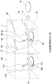
図1,図2は本発明の実施の形態にかかる洗浄装置1を示す図であり、図1はその概略平面図、図2はその概略側断面図である。これらの図に示すように洗浄装置1は、被洗浄物である半導体基板Wを支持する支持手段10と、支持手段10の周囲を囲って洗浄液の飛散を防止する洗浄カップ20と、洗浄カップ20の周囲を囲う洗浄槽30と、洗浄槽30内の所定位置に設置され前記半導体基板Wの表面を薬液洗浄する洗浄手段(薬液洗浄手段)40と、洗浄槽30内の所定位置に設置され前記半導体基板Wの表面をリンス洗浄する洗浄手段(リンス洗浄手段)50と、洗浄手段40,50とは別に洗浄槽30内の所定位置に設置され洗浄カップ20の内壁21を洗浄する洗浄手段70と、洗浄槽30内の所定位置に設置され洗浄槽30の内壁31を洗浄する洗浄手段80と、半導体基板Wをスクラブ洗浄する際に用いる洗浄アーム60とを具備して構成されている。
【0014】
支持手段10は半導体基板Wをその被処理面を上向きに開放した状態でほぼ水平に支持するものであり、具体的には半導体基板Wの外周をチャック機構13によって把持するように構成されている。支持手段10は、駆動部15によって回転駆動される。洗浄カップ20は前記支持手段10の周囲を囲むように、上面が開放されたカップ状に形成されている。洗浄槽30は洗浄カップ20を囲んで洗浄装置1の外壁を構成するものである。洗浄手段40と洗浄手段50は何れも液噴射ノズルより液体を半導体基板W表面に噴射するタイプの洗浄手段であり、洗浄手段40は薬液(例えば二次洗浄用の酸系薬液(DHF等))を噴射するもの、洗浄手段50はリンス液(例えば純水)を噴射するものである。
【0015】
洗浄手段70と洗浄手段80は何れも液噴射ノズルより洗浄液(例えば純水)を噴射するタイプの洗浄手段であって、洗浄手段70は洗浄液を洗浄カップ20の内壁21に向けて噴射し、洗浄手段80は洗浄液を洗浄槽30の内壁31に向けて噴射するように構成されている。
【0016】
図3は前記洗浄装置1を用いて、半導体基板Wの表面を平坦化させるためのポリッシングを終了した半導体基板Wに対して二種類の薬液洗浄処理を行なう洗浄装置設置例を示す概略構成図である。この洗浄装置設置例においては、洗浄装置(一次洗浄装置)100と、前記図1,図2に示す洗浄装置(二次洗浄装置)1とを併設している。洗浄装置100は液噴射ノズルより薬液(例えばNH4OH溶液)を半導体基板W表面に噴射するタイプの洗浄手段140と液噴射ノズルよりリンス液(例えば純水)を半導体基板W表面に噴射するタイプの洗浄手段150とスクラブ洗浄する際に用いる上面ロールスポンジ160及び下面ロールスポンジ165とを具備して構成されている。
【0017】
ここで図4は図3に示す洗浄装置設置例における洗浄プロセスフロー図である。以下各ステップについて説明する。
〔ステップ1〕ポリッシングの終了した半導体基板Wをまず洗浄装置100内に移送し、この半導体基板Wを回転しながらその表面に洗浄手段140から薬液を噴射・供給し、薬液洗浄する。このとき上面ロールスポンジ160と下面ロールスポンジ165を回転させつつ半導体基板W表面に擦り付けることでスクラブ洗浄を行なっても良い。
【0018】
〔ステップ2〕前記洗浄手段140による薬液の供給を停止した後、半導体基板Wを回転しながらその表面に洗浄手段150からリンス液を噴射・供給し、リンス洗浄する。このとき上面ロールスポンジ160と下面ロールスポンジ165を回転させつつ半導体基板W表面に擦り付けることでスクラブ洗浄を行なっても良い。
【0019】
〔ステップ3〕前記洗浄手段150によるリンス液の供給を停止した後、半導体基板Wを洗浄装置100から洗浄装置1内に移送して、図1,2に示す支持手段10上に保持する。次に支持手段10上に保持された半導体基板Wを、駆動部15によって回転駆動する。次に洗浄手段40の液噴射ノズルから薬液(DHF溶液)を噴射して薬液洗浄する。このとき洗浄アーム60を揺動して回転するスポンジ65を半導体基板W表面に擦り付けることでスクラブ洗浄を行なっても良い。このとき、洗浄装置100で用いて洗浄装置1に入り込んだ薬液と洗浄手段40が噴射した薬液とが化学反応を起こして生成された副生成物(NH4F)は、半導体基板Wの回転や装置内部の気流によって、半導体基板Wの表面だけでなく、洗浄カップ20の内壁21や洗浄槽30の内壁31に付着する場合がある。
【0020】
〔ステップ4〕次に前記洗浄手段40による薬液の供給を停止した後、洗浄手段50の液噴射ノズルからリンス液(純水)を噴射して半導体基板Wの表面をリンス洗浄する。このとき洗浄アーム60を揺動して回転するスポンジ65を半導体基板W表面に擦り付けることでスクラブ洗浄を行なっても良い。一方このリンス洗浄と同時に、両洗浄手段70,80の液噴射ノズルからも洗浄液(純水)を噴射することで洗浄カップ20の内壁21と洗浄槽30の内壁31とを洗浄する。これによって半導体基板Wに付着した薬液や副生成物のみならず、洗浄カップ20の内壁21と洗浄槽30の内壁31に付着した薬液や副生成物も確実に洗浄され除去される。洗浄手段70や洗浄手段80による洗浄液の噴射は、単なる洗浄液の噴霧や液噴射ノズルからの落下供給よりも、洗浄液にある程度の流体圧をかけて噴射する方が、洗浄カップ20の内壁21や洗浄槽30の内壁31に付着した薬液や副生成物の洗い落としに効果的である。洗浄液に加える流体圧としては、0.1(Mpa)以上が好適であるが、0.05(Mpa)以上であれば適用可能である。
【0021】
洗浄カップ20の内壁21と洗浄槽30の内壁31の洗浄タイミングとしては、要は薬液を供給していないときに行えば良いのであるが、通常は上記のように半導体基板Wをリンス洗浄しているときに同時に行う。しかし洗浄カップ20や洗浄槽30に噴きつけた後の副生成物等を含む洗浄液が半導体基板Wに落下してそのまま乾燥されないように、洗浄カップ20と洗浄槽30への洗浄液噴射を停止した後もしばらくは半導体基板Wへの洗浄手段50によるリンス液の供給を続けることが望ましい。また半導体基板Wが洗浄カップ20内に存在しないときに洗浄カップ20の内壁21と洗浄槽30の内壁31とを洗浄しても良い。
【0022】
〔ステップ5〕次に半導体基板Wへのリンス液の供給と、洗浄カップ20の内壁21と洗浄槽30の内壁31への洗浄液の噴射を停止した後、駆動部15によって半導体基板Wを高速回転することで、スピン乾燥する。このとき半導体基板Wのスピンによる気流が生じるが、洗浄カップ20の内壁21と洗浄槽30の内壁31は洗浄液で洗浄され、薬液や副生成物は付着していないので、内壁21,31の汚染による半導体基板Wの逆汚染は確実に防止される。これによって図3に示す洗浄装置設置例での洗浄処理が終了する。
【0023】
図5は以上のようにして乾燥されて洗浄装置1から取り出された半導体基板Wの表面の状態を示す図である。また図6は前記洗浄手段70,80を設置しないで洗浄手段40,50のみで洗浄して洗浄装置1から取り出された半導体基板Wの表面の状態を示す図である。両図において黒点は逆汚染(Defect)していることを示す部分である。両図に示すように、洗浄手段70,80によって洗浄カップ20の内壁21と洗浄槽30の内壁31とを洗浄することで、逆汚染が極めて効果的に防止されることがわかる。
【0024】
図7,図8は本発明の参考例にかかる洗浄装置1−2を示す図であり、図7はその概略平面図、図8はその概略側断面図である。この洗浄装置1−2において前記図1,図2に示す洗浄装置1と同一部分には同一符号を付してその詳細な説明は省略する。この洗浄装置1−2も、前記洗浄装置1と同様に、被洗浄物である半導体基板Wを支持する支持手段10と、支持手段10の周囲を囲って洗浄液の飛散を防止する洗浄カップ20と、洗浄カップ20の周囲を囲う洗浄槽30と、洗浄槽30内の所定位置に設置され前記半導体基板Wの表面を薬液洗浄する洗浄手段(薬液洗浄手段)40と、洗浄槽30内の所定位置に設置され前記半導体基板Wの表面をリンス洗浄する洗浄手段(リンス洗浄手段)50とを具備している。そしてこの洗浄装置1−2において前記図1,図2に示す洗浄装置1と相違する点は、洗浄装置70,80を設置する代わりに、支持手段10を洗浄液で洗浄する洗浄手段90を設けた点である。
【0025】
洗浄手段90は液噴射ノズルより洗浄液(例えば純水)を噴射するタイプの洗浄手段であって洗浄カップ20の側壁の四ヵ所に設けられており、洗浄液を洗浄カップ20の内側から支持手段10、特に支持手段10のチャック機構13の部分に向けて噴射するように取り付けられている。
【0026】
そしてこの洗浄装置1−2を前記図3に示す二次洗浄装置1に代えて用いた場合について説明する。なお図3では二次洗浄装置1内に洗浄手段70,80を記載しているが、その代わりに図7,図8に示す洗浄装置90が設置されているものとして説明する。図9はこの洗浄装置設置例における洗浄プロセスフロー図である。以下各ステップについて説明する。
【0027】
〔ステップ1〕ポリッシングの終了した半導体基板Wをまず洗浄装置100内に移送し、この半導体基板Wを回転しながらその表面に洗浄手段140から薬液を噴射・供給し、薬液洗浄する。このとき上面ロールスポンジ160と下面ロールスポンジ165を回転させつつ半導体基板W表面に擦り付けることでスクラブ洗浄を行なっても良い。
【0028】
〔ステップ2〕前記洗浄手段140による薬液の供給を停止した後、半導体基板Wを回転しながらその表面に洗浄手段150からリンス液を噴射・供給し、リンス洗浄する。このとき上面ロールスポンジ160と下面ロールスポンジ165を回転させつつ半導体基板W表面に擦り付けることでスクラブ洗浄を行なっても良い。
【0029】
〔ステップ3〕前記洗浄手段150によるリンス液の供給を停止した後、半導体基板Wを洗浄装置100から洗浄装置1内に移送して、図7,8に示す支持手段10上に保持する。次に支持手段10上に保持された半導体基板Wを、駆動部15によって回転駆動する。次に洗浄手段40の液噴射ノズルから薬液(DHF溶液)を噴射して薬液洗浄する。このとき洗浄アーム60を揺動して回転するスポンジ65を半導体基板W表面に擦り付けることでスクラブ洗浄を行なっても良い。このとき、洗浄装置100で用いて洗浄装置1に入り込んだ薬液と洗浄手段40が噴射した薬液とが化学反応を起こして生成された副生成物(NH4F)は、半導体基板Wの回転や装置内部の気流によって、半導体基板Wの表面だけでなく、洗浄カップ20の内壁21や洗浄槽30の内壁31に付着する場合がある。
【0030】
〔ステップ4〕次に前記洗浄手段40による薬液の供給を停止した後、洗浄手段50の液噴射ノズルからリンス液(純水)を噴射して半導体基板Wの表面をリンス洗浄する。このとき洗浄アーム60を揺動して回転するスポンジ65を半導体基板W表面に擦り付けることでスクラブ洗浄を行なっても良い。一方このリンス洗浄と同時に、図7,図8に示す洗浄手段90の液噴射ノズルからも洗浄液(純水)を噴射することで支持手段13のチャック機構13の部分や支持手段13のその他の部分を洗浄する。これによって半導体基板Wに付着した薬液や副生成物のみならず、支持手段10に付着した薬液や副生成物も確実に洗い流され除去される。洗浄手段90による洗浄液の噴射も、ある程度の流体圧をかけて噴射する方が、支持手段10に付着した薬液や副生成物の洗い落としに効果的である。洗浄液に加える流体圧としては、0.1(Mpa)以上が好適であるが、0.05(Mpa)以上であれば適用可能である。
【0031】
支持手段10の洗浄タイミングとしては、要は薬液を供給していないときに行えば良いのであるが、通常は上記のように半導体基板Wをリンス洗浄しているときに同時に行う。しかし支持手段10に噴きつけた後の副生成物等を含む洗浄液が半導体基板Wに付着してそのまま乾燥しないように、支持手段10への洗浄液噴射を停止した後もしばらくは半導体基板Wへの洗浄手段50によるリンス液の供給を続けることが望ましい。また半導体基板Wが洗浄カップ20内に存在しないときに支持手段10を洗浄しても良い。
【0032】
〔ステップ5〕次に半導体基板Wへのリンス液の供給と、支持手段10への洗浄液の噴射を停止した後、駆動部15によって半導体基板Wを高速回転することで、スピン乾燥する。このとき半導体基板Wのスピンによる気流が生じるが、支持手段10は洗浄液で洗浄され、薬液や副生成物は付着していないので、支持手段10の汚染による半導体基板Wの逆汚染は確実に防止される。これによって洗浄処理が終了する。
【0033】
以上本発明の実施形態を説明したが、本発明は上記実施形態に限定されるものではなく、特許請求の範囲、及び明細書と図面に記載された技術的思想の範囲内において種々の変形が可能である。なお直接明細書及び図面に記載がない何れの形状や構造や材質であっても、本願発明の作用・効果を奏する以上、本願発明の技術的思想の範囲内である。例えば上記実施の形態及び参考例では洗浄手段70及び洗浄手段80による洗浄カップ20の内壁21及び洗浄槽30の内壁31の洗浄と、洗浄手段90による支持手段10の洗浄とを別の実施の形態及び参考例としてそれぞれ説明したが、これら三つの洗浄手段70,80,90を1つの洗浄装置に組み込むことで、洗浄カップ20の内壁21の洗浄と洗浄槽30の内壁31の洗浄と支持手段10の洗浄とを行うように構成すれば、さらに半導体基板Wの逆汚染が効果的に防止できることは言うまでもない。
【0034】
また上記実施の形態及び参考例では、洗浄装置1,1−2を図3に示すように、ポリッシングを終了した半導体基板Wに対して二種類の薬液洗浄処理を行なう洗浄装置に利用した場合を説明したが、三種類以上の薬液洗浄処理を行なう洗浄装置に利用してもよいことは言うまでもない。複数種類の薬液を用いてそれぞれ別々の洗浄装置において洗浄処理を行なう場合、最終段の洗浄装置(又は必要に応じて途中段階の洗浄装置)として本発明及び参考例にかかる洗浄装置1,1−2を用いれば、洗浄装置1,1−2に至るまでの洗浄工程で生じた汚染物質が洗浄装置1,1−2から排出される半導体基板W上には付着せず、好適である。なお本発明及び参考例にかかる洗浄装置1,1−2を、単体で使用してもよいことは言うまでもない。
【0035】
また図1,図2に示す実施の形態では洗浄カップ20の内壁21を洗浄する洗浄手段70と、洗浄槽30の内壁31を洗浄する洗浄手段80とを別々に設置したが、一つの噴射ノズルで洗浄カップ20の内壁21と洗浄槽30の内壁31とに同時に洗浄液が噴射できるように構成すれば、これら洗浄手段70,80を一体に構成してもよい。また上記各実施の形態では洗浄後の半導体基板Wの乾燥方法としてスピンによる乾燥方法を用いたが、洗浄カップ内で乾燥させるものであれば他の乾燥方法を用いても良い。また支持手段10による半導体基板Wの支持構造や、洗浄カップ20と洗浄槽30の形状・構造などに種々の変更が可能であることは言うまでもない。
【0036】
【発明の効果】
以上詳細に説明したように本発明によれば、同一洗浄装置内で洗浄処理と乾燥処理とを行なっても、乾燥後の被洗浄物が逆汚染される恐れはなくなる。
【図面の簡単な説明】
【図1】本発明の実施の形態にかかる洗浄装置1を示す概略平面図である。
【図2】本発明の実施の形態にかかる洗浄装置1を示す概略側断面図である。
【図3】洗浄装置1を用いて、ポリッシングを終了した半導体基板Wに対して二種類の薬液洗浄処理を行なう洗浄装置設置例を示す概略構成図である。
【図4】洗浄プロセスフロー図である。
【図5】洗浄装置1から取り出された半導体基板Wの表面の状態を示す図である。
【図6】洗浄手段40,50のみで洗浄して洗浄装置1から取り出された半導体基板Wの表面の状態を示す図である。
【図7】 本発明の参考例にかかる洗浄装置1−2を示す概略平面図である。
【図8】 本発明の参考例にかかる洗浄装置1−2を示す概略側断面図である。
【図9】洗浄プロセスフロー図である。
【符号の説明】
1 洗浄装置
W 半導体基板(被洗浄物)
10 支持手段
13 チャック機構
15 駆動部
20 洗浄カップ
21 内壁
30 洗浄槽
31 内壁
40 洗浄手段(薬液洗浄手段)
50 洗浄手段(リンス洗浄手段)
60 洗浄アーム
65 スポンジ
70 洗浄手段(洗浄カップ内壁洗浄手段)
80 洗浄手段(洗浄槽内壁洗浄手段)
100 洗浄装置(一次洗浄装置)
101 ロールブラシ
1−2 洗浄装置
90 洗浄手段(支持手段洗浄手段)[0001]
BACKGROUND OF THE INVENTION
The present invention relates to a washing method, is particularly a semiconductor substrate, a glass substrate, of a preferred wash method for cleaning a substrate a high degree of cleanliness such as a liquid crystal panel is required.
[0002]
[Prior art]
In recent years, circuit wiring on a semiconductor substrate is miniaturized and the distance between wirings is becoming narrower as semiconductor devices are highly integrated. In the processing of a semiconductor substrate, particles such as fine particles, dust, and crystalline protrusions of a semiconductor piece may adhere, and if particles larger than the distance between the wirings remain, problems such as short-circuiting of the wiring occur. Therefore, the particles present on the substrate must be sufficiently smaller than the distance between the wirings. Such a situation also applies to the processing of a glass substrate used for a mask or the like or a substrate such as a liquid crystal panel. Along with such a demand, there is a need for a cleaning technique for dropping finer submicron level particles from a semiconductor substrate or the like.
[0003]
As a method of cleaning a semiconductor substrate that has been polished to flatten the substrate surface, scrub cleaning performed by rubbing a cleaning body made of a brush, a sponge or the like while supplying a cleaning liquid to a rotating substrate, or ultrasonic In general, there is known a liquid jet cleaning performed by spraying a cleaning liquid or a high-pressure cleaning liquid to which a vibration energy is applied toward a rotating substrate. Then, the substrate after the cleaning process is completed is dried by spinning, for example.
[0004]
As a cleaning apparatus for performing such cleaning, a support means for supporting the substrate, a cleaning cup that surrounds the periphery of the support means and prevents the cleaning liquid from being scattered by the centrifugal force accompanying the rotation of the substrate and contaminating the outside And a washing tank covering the periphery of the washing cup.
[0005]
When the substrate is cleaned using two types of chemical solutions, two primary and secondary units are provided as cleaning devices, and after cleaning with one chemical solution in the primary cleaning device, the other in the secondary cleaning device In the secondary cleaning device, cleaning with pure water is performed, followed by rinsing with pure water, followed by drying (for example, spin dry processing) in the secondary cleaning device, and then taking it out.
[0006]
However, if the drying process of the substrate after the secondary cleaning process is performed in the secondary cleaning apparatus, the substrate may be back-contaminated. That is, for example, when an alkaline chemical (for example, NH 4 OH) is used for chemical cleaning in the primary cleaning device, and an acidic chemical (for example, DHF) is used for chemical cleaning in the secondary cleaning device, it is transferred to the secondary cleaning device. The acid adhering to the formed substrate reacts with the newly supplied alkali to produce a by-product (for example, NH 4 OH + HF → H 2 O + NH 4 F (by-product)), which is a secondary cleaning device. It adheres and accumulates in the washing cup and washing tank inside. Since the substrate itself in the secondary cleaning apparatus is then rinsed with pure water, the chemicals and by-products are removed, but the by-products and chemicals accumulated on the cleaning cup and the inner wall of the cleaning tank are accumulated. Since they remain attached, they are wound up by the air current when the substrate is spin-dried, and adhere to the substrate after rinsing and are decontaminated (defects increase).
[0007]
In order to solve the above problem, a separate drying device may be provided in addition to the primary and secondary cleaning devices, and the substrate after the rinse cleaning may be dried in this non-contaminated drying device. However, when this method is used, the number of processing units becomes three, which not only increases the installation area by increasing the size of the apparatus, but also complicates the transfer and control of the substrate between the units, thereby reducing the transfer throughput. End up.
[0008]
[Problems to be solved by the invention]
The present invention has been made in view of the above points and its object is also subjected to a washing treatment and a drying treatment in the same washing device, not the name of the risk that the object to be cleaned after drying is reversely contaminated wash It is to provide a purification method.
[0009]
[Means for Solving the Problems]
In the present invention, after performing a chemical solution cleaning process for cleaning an object to be cleaned in a cleaning cup, cleaning of the inner wall of the cleaning cup is performed by spraying a cleaning solution from a cleaning means installed in a cleaning tank surrounding the cleaning cup. A step of cleaning the inner wall of the cleaning tank by spraying a cleaning liquid from a cleaning means installed in the cleaning tank, a rinsing cleaning process for rinsing and cleaning the object to be cleaned, and a supporting means for supporting the object to be cleaned Supplying the cleaning liquid and performing cleaning simultaneously, and the rinsing cleaning process is performed after the cleaning of the inner wall of the cleaning cup, the cleaning of the inner wall of the cleaning tank, and the cleaning of the support means, and after the rinsing cleaning process It is a cleaning method characterized by performing a drying step of drying an object to be cleaned in a cleaning cup. As a result, the inner wall of the cleaning cup, the inner wall of the cleaning tank, and the support means are cleaned, and contaminants attached to these inner walls and the support means are surely removed. Therefore, even if the object to be cleaned is cleaned in this cleaning apparatus, the object to be cleaned after cleaning is caused by contaminants adhering to the inner wall of the cleaning cup, the inner wall of the cleaning tank, and the supporting means . Will not be back contaminated. This eliminates the need for a separate drying device, reducing the installation area and cost, and simplifies the transfer and control of objects to be cleaned between each unit, improving the transfer throughput. To do.
[0013]
DETAILED DESCRIPTION OF THE INVENTION
Hereinafter, embodiments of the present invention will be described in detail with reference to the drawings.
1 and 2 are views showing a
[0014]
The support means 10 supports the semiconductor substrate W substantially horizontally with its processing surface open upward, and is specifically configured to hold the outer periphery of the semiconductor substrate W by the
[0015]
Each of the cleaning means 70 and the cleaning means 80 is a type of cleaning means for injecting a cleaning liquid (for example, pure water) from a liquid injection nozzle. The cleaning means 70 injects the cleaning liquid toward the
[0016]
FIG. 3 is a schematic configuration diagram showing an example of installation of a cleaning apparatus for performing two types of chemical cleaning processes on the semiconductor substrate W that has been polished for flattening the surface of the semiconductor substrate W using the
[0017]
Here, FIG. 4 is a cleaning process flow chart in the cleaning apparatus installation example shown in FIG. Each step will be described below.
[Step 1] The semiconductor substrate W after polishing is first transferred into the
[0018]
[Step 2] After the supply of the chemical solution by the cleaning means 140 is stopped, the rinse liquid is sprayed and supplied from the cleaning means 150 to the surface of the semiconductor substrate W while rotating, thereby performing the rinse cleaning. At this time, scrub cleaning may be performed by rubbing against the surface of the semiconductor substrate W while rotating the upper
[0019]
[Step 3] After the supply of the rinsing liquid by the cleaning means 150 is stopped, the semiconductor substrate W is transferred from the
[0020]
[Step 4] Next, after the supply of the chemical solution by the cleaning means 40 is stopped, a rinse liquid (pure water) is sprayed from the liquid spray nozzle of the cleaning means 50 to rinse the surface of the semiconductor substrate W. At this time, scrub cleaning may be performed by rubbing the
[0021]
The cleaning timing of the
[0022]
[Step 5] Next, the supply of the rinsing liquid to the semiconductor substrate W and the spraying of the cleaning liquid onto the
[0023]
FIG. 5 is a view showing the state of the surface of the semiconductor substrate W that has been dried and taken out from the
[0024]
7 and 8 are views showing a cleaning apparatus 1-2 according to a reference example of the present invention, FIG. 7 is a schematic plan view thereof, and FIG. 8 is a schematic side sectional view thereof. In this cleaning device 1-2, the same parts as those in the
[0025]
The cleaning means 90 is a type of cleaning means for injecting a cleaning liquid (for example, pure water) from a liquid injection nozzle, and is provided at four locations on the side wall of the cleaning
[0026]
The case where the cleaning device 1-2 is used in place of the
[0027]
[Step 1] The semiconductor substrate W after polishing is first transferred into the
[0028]
[Step 2] After the supply of the chemical solution by the cleaning means 140 is stopped, the rinse liquid is sprayed and supplied from the cleaning means 150 to the surface of the semiconductor substrate W while rotating, thereby performing the rinse cleaning. At this time, scrub cleaning may be performed by rubbing against the surface of the semiconductor substrate W while rotating the upper
[0029]
[Step 3] After the supply of the rinsing liquid by the cleaning means 150 is stopped, the semiconductor substrate W is transferred from the
[0030]
[Step 4] Next, after the supply of the chemical solution by the cleaning means 40 is stopped, a rinse liquid (pure water) is sprayed from the liquid spray nozzle of the cleaning means 50 to rinse the surface of the semiconductor substrate W. At this time, scrub cleaning may be performed by rubbing the
[0031]
The
[0032]
[Step 5] Next, after the supply of the rinsing liquid to the semiconductor substrate W and the spraying of the cleaning liquid to the support means 10 are stopped, the semiconductor substrate W is rotated at a high speed by the driving
[0033]
Although the embodiments of the present invention have been described above, the present invention is not limited to the above-described embodiments, and various modifications can be made within the scope of the technical idea described in the claims and the specification and drawings. Is possible. Note that any shape, structure, or material not directly described in the specification and drawings is within the scope of the technical idea of the present invention as long as the effects and advantages of the present invention are exhibited. For example, in the above embodiment and the reference example , the cleaning of the
[0034]
Further, in the above-described embodiment and reference example , as shown in FIG. 3, the
[0035]
In the embodiment shown in FIGS. 1 and 2, the cleaning means 70 for cleaning the
[0036]
【The invention's effect】
As described above in detail, according to the present invention, there is no possibility that the object to be cleaned after being dried is back-contaminated even if the cleaning process and the drying process are performed in the same cleaning apparatus.
[Brief description of the drawings]
FIG. 1 is a schematic plan view showing a
FIG. 2 is a schematic sectional side view showing the
FIG. 3 is a schematic configuration diagram showing an example of installation of a cleaning apparatus that performs two types of chemical liquid cleaning processes on a semiconductor substrate W that has been polished using the
FIG. 4 is a flowchart of a cleaning process.
5 is a view showing a state of the surface of a semiconductor substrate W taken out from the
6 is a view showing a state of the surface of a semiconductor substrate W which is cleaned only by cleaning
FIG. 7 is a schematic plan view showing a cleaning device 1-2 according to a reference example of the present invention.
FIG. 8 is a schematic sectional side view showing a cleaning apparatus 1-2 according to a reference example of the present invention.
FIG. 9 is a flowchart of a cleaning process.
[Explanation of symbols]
1 Cleaning device W Semiconductor substrate (object to be cleaned)
DESCRIPTION OF
50 Cleaning means (rinse cleaning means)
60
80 Cleaning means (cleaning inner wall cleaning means)
100 Cleaning device (Primary cleaning device)
101 Roll brush 1-2
Claims (1)
前記洗浄カップ内壁の洗浄を洗浄カップの周囲を囲う洗浄槽に設置した洗浄手段からの洗浄液の噴射によって行う工程と、
洗浄槽内壁の洗浄を洗浄槽に設置した洗浄手段からの洗浄液の噴射によって行う工程と、
被洗浄物をリンス洗浄するリンス洗浄工程と、
前記被洗浄物を支持している支持手段に洗浄液を供給して洗浄する工程と、
を同時に行うと共に、
前記リンス洗浄工程は前記洗浄カップ内壁の洗浄及び洗浄槽内壁の洗浄及び支持手段の洗浄の停止後も行い、
前記リンス洗浄工程の後に前記洗浄カップ内で被洗浄物を乾燥させる乾燥工程を行うことを特徴とする洗浄方法。 After performing the chemical cleaning process to clean the target object in the cleaning cup,
A step of cleaning the inner wall of the cleaning cup by spraying a cleaning liquid from a cleaning unit installed in a cleaning tank surrounding the cleaning cup;
A step of cleaning the inner wall of the cleaning tank by spraying a cleaning liquid from a cleaning means installed in the cleaning tank;
A rinse cleaning step for rinsing and cleaning the object to be cleaned;
Supplying a cleaning liquid to the supporting means supporting the object to be cleaned, and cleaning,
At the same time,
The rinse cleaning step is also performed after the cleaning of the inner wall of the cleaning cup and the cleaning of the inner wall of the cleaning tank and the cleaning of the support means,
A cleaning method comprising performing a drying step of drying an object to be cleaned in the cleaning cup after the rinse cleaning step.
Priority Applications (3)
| Application Number | Priority Date | Filing Date | Title |
|---|---|---|---|
| JP2002202812A JP4017463B2 (en) | 2002-07-11 | 2002-07-11 | Cleaning method |
| US10/614,295 US7264681B2 (en) | 2002-07-11 | 2003-07-08 | Cleaning apparatus and cleaning method |
| US11/882,565 US20080000509A1 (en) | 2002-07-11 | 2007-08-02 | Cleaning apparatus and cleaning method |
Applications Claiming Priority (1)
| Application Number | Priority Date | Filing Date | Title |
|---|---|---|---|
| JP2002202812A JP4017463B2 (en) | 2002-07-11 | 2002-07-11 | Cleaning method |
Publications (3)
| Publication Number | Publication Date |
|---|---|
| JP2004047714A JP2004047714A (en) | 2004-02-12 |
| JP2004047714A5 JP2004047714A5 (en) | 2005-07-21 |
| JP4017463B2 true JP4017463B2 (en) | 2007-12-05 |
Family
ID=31708898
Family Applications (1)
| Application Number | Title | Priority Date | Filing Date |
|---|---|---|---|
| JP2002202812A Expired - Lifetime JP4017463B2 (en) | 2002-07-11 | 2002-07-11 | Cleaning method |
Country Status (2)
| Country | Link |
|---|---|
| US (2) | US7264681B2 (en) |
| JP (1) | JP4017463B2 (en) |
Families Citing this family (15)
| Publication number | Priority date | Publication date | Assignee | Title |
|---|---|---|---|---|
| US8316866B2 (en) * | 2003-06-27 | 2012-11-27 | Lam Research Corporation | Method and apparatus for cleaning a semiconductor substrate |
| US6936540B2 (en) * | 2003-09-18 | 2005-08-30 | Micron Technology, Inc. | Method of polishing a semiconductor substrate, post-CMP cleaning process, and method of cleaning residue from registration alignment markings |
| JP4691887B2 (en) * | 2004-03-04 | 2011-06-01 | パナソニック株式会社 | Pattern forming method, pattern forming apparatus, and method for manufacturing member for plasma display |
| US20060157080A1 (en) * | 2005-01-20 | 2006-07-20 | Teng-Chun Tsai | Cleaning method for semiconductor wafer |
| SG154438A1 (en) * | 2005-12-30 | 2009-08-28 | Lam Res Corp | Cleaning compound and method and system for using the cleaning compound |
| US9140704B2 (en) | 2007-07-26 | 2015-09-22 | Temple University Of The Commonwealth System Of Higher Education | Serum markers associated with early and other stages of breast cancer |
| JP5220447B2 (en) * | 2008-03-17 | 2013-06-26 | 東京エレクトロン株式会社 | Substrate processing system cleaning method, storage medium, and substrate processing system |
| JP5864232B2 (en) * | 2011-02-01 | 2016-02-17 | 東京エレクトロン株式会社 | Liquid processing apparatus and liquid processing method |
| JP6295023B2 (en) | 2012-10-03 | 2018-03-14 | 株式会社荏原製作所 | Substrate cleaning apparatus, substrate cleaning method, and polishing apparatus |
| CN103977973B (en) * | 2014-05-09 | 2016-10-05 | 欧蒙医学诊断(中国)有限公司 | A kind of slide glass cleans apparatus and method |
| US10155252B2 (en) * | 2015-04-30 | 2018-12-18 | Taiwan Semiconductor Manufacturing Co., Ltd. | Semiconductor apparatus and washing method |
| JP7058550B2 (en) * | 2018-05-16 | 2022-04-22 | 東京エレクトロン株式会社 | Development processing equipment and development processing method |
| CN110355157A (en) * | 2019-07-29 | 2019-10-22 | 南京诺尔曼生物技术有限公司 | Sample needle cleaning device and component |
| CN112588680B (en) * | 2020-12-16 | 2022-04-22 | 无锡先导智能装备股份有限公司 | Cleaning device and cleaning equipment |
| WO2023195340A1 (en) * | 2022-04-05 | 2023-10-12 | 東京エレクトロン株式会社 | Substrate processing device and substrate processing method |
Family Cites Families (18)
| Publication number | Priority date | Publication date | Assignee | Title |
|---|---|---|---|---|
| US3990462A (en) * | 1975-05-19 | 1976-11-09 | Fluoroware Systems Corporation | Substrate stripping and cleaning apparatus |
| US4161356A (en) * | 1977-01-21 | 1979-07-17 | Burchard John S | Apparatus for in-situ processing of photoplates |
| US4788994A (en) * | 1986-08-13 | 1988-12-06 | Dainippon Screen Mfg. Co. | Wafer holding mechanism |
| JPS63173327A (en) * | 1987-01-13 | 1988-07-16 | Nec Corp | Production equipment for semiconductor device |
| JPH04196425A (en) * | 1990-11-28 | 1992-07-16 | Sigma Merutetsuku Kk | Chemicals processing apparatus |
| US5265632A (en) * | 1991-05-08 | 1993-11-30 | Tokyo Electron Limited | Cleaning apparatus |
| JPH08323302A (en) | 1995-05-29 | 1996-12-10 | Dainippon Screen Mfg Co Ltd | Substrate treating device |
| JP3414916B2 (en) * | 1996-02-27 | 2003-06-09 | 大日本スクリーン製造株式会社 | Substrate processing apparatus and method |
| JPH09290199A (en) * | 1996-04-25 | 1997-11-11 | Dainippon Screen Mfg Co Ltd | Cup cleaning device and rotating type substrate processing device |
| JPH10144599A (en) | 1996-11-11 | 1998-05-29 | Tokyo Electron Ltd | Rotary treatment equipment and its washing method |
| JPH10199852A (en) * | 1997-01-13 | 1998-07-31 | Dainippon Screen Mfg Co Ltd | Rotary substrate treatment device |
| JPH11283948A (en) * | 1998-03-27 | 1999-10-15 | Dainippon Screen Mfg Co Ltd | Substrate rotation processing device |
| JP2000114219A (en) * | 1998-10-06 | 2000-04-21 | Toshiba Corp | Substrate-processing device |
| US6290865B1 (en) * | 1998-11-30 | 2001-09-18 | Applied Materials, Inc. | Spin-rinse-drying process for electroplated semiconductor wafers |
| JP3587723B2 (en) * | 1999-04-30 | 2004-11-10 | 東京エレクトロン株式会社 | Substrate processing apparatus and substrate processing method |
| JP2000334395A (en) | 1999-05-31 | 2000-12-05 | Ebara Corp | Cleaning apparatus |
| US6516815B1 (en) | 1999-07-09 | 2003-02-11 | Applied Materials, Inc. | Edge bead removal/spin rinse dry (EBR/SRD) module |
| JP2002009035A (en) * | 2000-06-26 | 2002-01-11 | Toshiba Corp | Method and device for washing substrate |
-
2002
- 2002-07-11 JP JP2002202812A patent/JP4017463B2/en not_active Expired - Lifetime
-
2003
- 2003-07-08 US US10/614,295 patent/US7264681B2/en not_active Expired - Lifetime
-
2007
- 2007-08-02 US US11/882,565 patent/US20080000509A1/en not_active Abandoned
Also Published As
| Publication number | Publication date |
|---|---|
| US20040065352A1 (en) | 2004-04-08 |
| US7264681B2 (en) | 2007-09-04 |
| JP2004047714A (en) | 2004-02-12 |
| US20080000509A1 (en) | 2008-01-03 |
Similar Documents
| Publication | Publication Date | Title |
|---|---|---|
| US20080000509A1 (en) | Cleaning apparatus and cleaning method | |
| TWI397116B (en) | Substrate processing apparatus and substrate processing method | |
| JP3865602B2 (en) | Substrate cleaning device | |
| US7699939B2 (en) | Substrate cleaning method | |
| TW201330148A (en) | Substrate cleaning method and substrate cleaning device | |
| KR200477678Y1 (en) | Wafer cleaning device of chemical mechanical polishing equipment | |
| CN113327841B (en) | Wafer cleaning system and cleaning method capable of keeping cleaning roller clean | |
| KR100695980B1 (en) | Substrate cleaning apparatus | |
| JP2010021457A (en) | Method of cleaning brush | |
| US20100108095A1 (en) | Substrate processing apparatus and substrate cleaning method | |
| JPH11297652A (en) | Substrate treatment apparatus | |
| KR101017102B1 (en) | Wet type washing device of wafer and thereof method | |
| JP2002124504A (en) | Substrate cleaner and substrate cleaning method | |
| JP4033709B2 (en) | Substrate cleaning method and apparatus | |
| JP7525242B2 (en) | Substrate processing apparatus and substrate processing method | |
| KR20110077705A (en) | The apparatus and method for cleaning single wafer | |
| JP2000114219A (en) | Substrate-processing device | |
| JP2930580B1 (en) | Cleaning equipment for semiconductor wafers | |
| JP4330209B2 (en) | Substrate cleaning method | |
| JP4425947B2 (en) | Substrate cleaning method | |
| JP2000208466A (en) | Method and apparatus for treating substrate | |
| JP2000040684A (en) | Cleaning equipment | |
| JP2001217218A (en) | Device and method for treating wafer | |
| JP2001334219A (en) | Spin treatment device and spin treatment method | |
| KR20090069380A (en) | Scrubber equipped with hf module and wafer cleaning method using thereof |
Legal Events
| Date | Code | Title | Description |
|---|---|---|---|
| A521 | Request for written amendment filed |
Free format text: JAPANESE INTERMEDIATE CODE: A821 Effective date: 20041126 Free format text: JAPANESE INTERMEDIATE CODE: A523 Effective date: 20041126 |
|
| A621 | Written request for application examination |
Free format text: JAPANESE INTERMEDIATE CODE: A621 Effective date: 20041126 |
|
| A977 | Report on retrieval |
Free format text: JAPANESE INTERMEDIATE CODE: A971007 Effective date: 20070202 |
|
| A131 | Notification of reasons for refusal |
Free format text: JAPANESE INTERMEDIATE CODE: A131 Effective date: 20070320 |
|
| A521 | Request for written amendment filed |
Free format text: JAPANESE INTERMEDIATE CODE: A523 Effective date: 20070516 Free format text: JAPANESE INTERMEDIATE CODE: A821 Effective date: 20070516 |
|
| A02 | Decision of refusal |
Free format text: JAPANESE INTERMEDIATE CODE: A02 Effective date: 20070612 |
|
| A521 | Request for written amendment filed |
Free format text: JAPANESE INTERMEDIATE CODE: A821 Effective date: 20070720 Free format text: JAPANESE INTERMEDIATE CODE: A523 Effective date: 20070720 |
|
| A911 | Transfer to examiner for re-examination before appeal (zenchi) |
Free format text: JAPANESE INTERMEDIATE CODE: A911 Effective date: 20070817 |
|
| TRDD | Decision of grant or rejection written | ||
| A01 | Written decision to grant a patent or to grant a registration (utility model) |
Free format text: JAPANESE INTERMEDIATE CODE: A01 Effective date: 20070911 |
|
| A61 | First payment of annual fees (during grant procedure) |
Free format text: JAPANESE INTERMEDIATE CODE: A61 Effective date: 20070918 |
|
| R150 | Certificate of patent or registration of utility model |
Ref document number: 4017463 Country of ref document: JP Free format text: JAPANESE INTERMEDIATE CODE: R150 Free format text: JAPANESE INTERMEDIATE CODE: R150 |
|
| FPAY | Renewal fee payment (event date is renewal date of database) |
Free format text: PAYMENT UNTIL: 20100928 Year of fee payment: 3 |
|
| FPAY | Renewal fee payment (event date is renewal date of database) |
Free format text: PAYMENT UNTIL: 20110928 Year of fee payment: 4 |
|
| R250 | Receipt of annual fees |
Free format text: JAPANESE INTERMEDIATE CODE: R250 |
|
| FPAY | Renewal fee payment (event date is renewal date of database) |
Free format text: PAYMENT UNTIL: 20120928 Year of fee payment: 5 |
|
| R250 | Receipt of annual fees |
Free format text: JAPANESE INTERMEDIATE CODE: R250 |
|
| FPAY | Renewal fee payment (event date is renewal date of database) |
Free format text: PAYMENT UNTIL: 20130928 Year of fee payment: 6 |
|
| R250 | Receipt of annual fees |
Free format text: JAPANESE INTERMEDIATE CODE: R250 |
|
| R250 | Receipt of annual fees |
Free format text: JAPANESE INTERMEDIATE CODE: R250 |
|
| R250 | Receipt of annual fees |
Free format text: JAPANESE INTERMEDIATE CODE: R250 |
|
| R250 | Receipt of annual fees |
Free format text: JAPANESE INTERMEDIATE CODE: R250 |
|
| R250 | Receipt of annual fees |
Free format text: JAPANESE INTERMEDIATE CODE: R250 |
|
| R250 | Receipt of annual fees |
Free format text: JAPANESE INTERMEDIATE CODE: R250 |
|
| R250 | Receipt of annual fees |
Free format text: JAPANESE INTERMEDIATE CODE: R250 |
|
| R250 | Receipt of annual fees |
Free format text: JAPANESE INTERMEDIATE CODE: R250 |
|
| R250 | Receipt of annual fees |
Free format text: JAPANESE INTERMEDIATE CODE: R250 |
|
| R250 | Receipt of annual fees |
Free format text: JAPANESE INTERMEDIATE CODE: R250 |
|
| EXPY | Cancellation because of completion of term |